


FX-2DA
SPECIAL FUNCTION BLOCK
USER'S GUIDE
JY992D52801C
This manual contains text, diagrams and explanations which will guide the reader in the correct installation
and operation of the FX-2DA special function block and should be read and understood before attempting
to install or use the unit.
Further information can be found in the FX PROGRAMMING MANUAL and FX SERIES HARDWARE
MANUAL.
1
●
The FX-2DA analog special function block has two output channels. The output channels take a digital value
and output an equivalent analog signal. This is called a D/A conversion. The FX-2DA has a maximum
resolution of 12 bits.
●
The selection of voltage or current based input/output is by user wiring. Analog ranges of -10 to 10V
(resolution: 5mV), and/or 4 to 20mA (resolution: 20µA) maybe selected.
●
FX programmable controllers versions 2.0 or later (those with serial number 13XXXX or larger) are
required; as these units have the TO/FROM applied instructions in their instruction set. Data transfer
between the FX-2DA and the FX base unit is by buffer memory exchange. There are 32 buffer memories
(each of 16 bits) in the FX-2DA.
●
The FX-2DA occupies 8 points of I/O on the FX, FX2C expansion bus. The 8 points can be allocated from
either inputs or outputs. The FX-2DA draws 30mA from the 5V rail of the base unit or powered extension
unit.
INTRODUCTION

1.1 External dimensions Weight : Approx. 0.5kg (1.1 lbs) Dimensions : mm (inches)
2
Extension cable
and connector
Any connection to these terminals
may damage the FX-2DA.
M3.5 (0.14)
terminal screws
24V LED
63 (2.48)
73 (2.87)
Wiring
D-A LED
125 (4.92)
140 (5.51)
1
0 (
0.39)
95 (3.74)
Groove for
35mm (1.38)
wide DIN rail
2-5.5mm (0.22)
hole
DC24V ±10% 130mA
Class 3
Grounding
(100 Ω or less)
*4
PC
+24V
0V
DC/DC
converter
FX-2DA special function block
Extension cable
*1 Use a twisted pair shielded cable for the analog
output. This cable should be wired away from
power lines or any other lines which could induce
noise.
*2 Apply 1-point grounding at the load side of the
output cable (class 3 grounding: 100 Ω or less). If
electrical noise is caused from grounding,
disconnect from grounding.
*3 If electrical noise or a voltage ripple exists at the
output, connect a smoothing capacitor of 0.1 to
0.47 µF, 25V.
Voltage output
V
+
V
I
I
V
V
I
I
*1
+
-
+
-
Current output
+
-
*1
*2
*2
Inverter,
etc.
*3
Recorder,
etc.
AG
+15V
-15V
CH1
CH2
*4 Connect the ground terminal on the FX-2DA with
the ground terminal on the base unit of the
programmable controller. Use class 3 grounding
on the base unit, if available.
Caution;
(a) The same output channel cannot drive current
and voltage output loads at the same time!
(b) Shorting the voltage output terminals may da-
mage the unit!
3
INSTALLATION NOTES AND USAGE
3.1 Environment specification
Item
Environment specifications
3.2 Power supply specifications
Item
Analog circuits
Digital circuits
3.3 Performance specifications
Item
Voltage or current outputs can be individually selected with each output
Max. convertible
output range
Digital input
(external load: 1kΩ
Voltage = -2048 to +2047
Same as those for the FX base unit
24V DC ±10% 130mA
(external power supply)
(internal power supply from base unit)
Voltage output
terminal. There are a total of 2 output points.
DC -10V to +10V
to 1MΩ)
(external load: 500 Ω or less)
Specification
Specification
5V DC, 30mA
Current output
DC+4mA to +20mA
Current = 0 to +1000
Resolution
Overall accuracy
Conversion speed
5mV (10V full scale 1/2000)
±1% full scale (10V range)
20µA (20mA full scale 1/1000)
±1% full scale (20mA range)
18ms for 2 channels (normal speed), 3.5ms for 2 channels (high speed).
Analog output continued...
Factory Presets
Load:
ΩΩ
= 10k
(voltage
Ω
ΩΩ
Output)
ΩΩ
= 250
Ω
(current
ΩΩ
Output)
Analog output
-2000 -1000
-2048
-10.24V
+10V
+ 5V
+10.235V
0 +1000 +2000
- 5V
Digital input
-10V
+2047
+20mA
Analog output
+ 4mA
Gain and offset can be adjusted using the procedure described in chapter 4.
0 1000
Digital input

Specification
Photo-coupler isolation between analog and digital circuits.
DC/DC converter isolation of power from FX base unit.
No isolation between analog channels.
8 points taken from the FX expansion bus
(can be either inputs or outputs)
Item
Isolation
Number of occupied I/O
points
ATTENTION FOR WHEN SWITCHING SYSTEM ON/OFF
Due to the inevitable timing difference of the DC24V for the analog circuits and other power lines of the
base unit, the output of the FX-2DA special function block may behave erroneously before settling down
to operational conditions in approximately 1sec. Therefore, ensure that this behavior is taken into account
such that the end performance of the system is not degraded.
(example)
Power switch
Miscellaneous
DC24V
supply
FX-2DA special
function block
cut analog lines
before switching
External analog
machine

3.4 Allocation of buffer memories (BFM)
BFM
*# 0
*# 1
*# 2
# 3-# 4
*# 5
# 6
*# 7
# 8-#19
contents
channel Initialization (Default = H00)
channel 1
channel 2
Reserved
Last data reset (Default = 0)
Reserved
selection of A-D
conversion speed
see note
When set to 0, normal
speed is selected 18ms
When set to 1, high
speed is selected 3.5ms
Reserved
In BFM's (buffer memory) with an “ * ”, data
can be written from the programmable controller using the TO command.
These BFM's should always be given when the
programmable controller goes from STOP to
RUN. Buffer memory (BFM's) are reset to their
default settings upon power on.
BFM
*#20
*#21
*#22
*#23
*#24
#25-#28
#29
#30
#31
b3 b2 b1 b0
Reset all to default default value: 0
Gain/offset adjust prohibit
Pro-
Permit
Initial value (0,1)
Offset/gain
G2 O2 G1 O1
hibit
setting command
Offset data (in mV or µA units)
default value: 0
Gain data (in mV or µA units)
default value: 5,000
Reserved
Error status (See next page)
Identification code K3010 (See next page)
Reserved
●
The buffer memory also handles information
used to adjust the gain and offsets of the FX2DA unit. Status of the unit such as errors
are also available.
●
From BFM #29 and #30, data can be read
via the FROM command.
●
Offset value : the actual output value when
the digital input is 0.
●
Gain value : the actual output value when
the digital input is +1000.

(1) Channel Selection
Switching between voltage and current output modes. The value of BFM #0 switches the analog output
between voltage and current on channels CH1 and CH2. It takes the form of a 2-character HEX number.
The least significant character controls CH1 and the other controls CH2.
Control of each O HEX character of
HOO
O=0 Voltage output (-10V to +10V)
Example : H10 CH1 : Voltage output CH2 Current output
:
:
O=1 Current output (+4mA to +20mA)
:
:
(2) Last data reset
If the programmable controller is changed to the STOP state, the FX-2DA will continue to output the last
value. To reset the output to the offset value, set the HEX characters of BFM #5 to one of the appropriate
settings below:
H01 : CH2=Hold, CH1=Reset
H10 : CH2=Reset, CH1=Hold
H11 : CH2=Reset, CH1=Reset
Both channels are held when BFM #5 = H00.
(3) Digital to Analog conversion speed change
By writing 0 or 1 into BFM #7 of the FX-2DA, the speed at which D-A conversion is performed can be
changed. However the following points should be noted:
Note :
●
The conversion speed does not depend on the number of channels being used.
●
On power up, the FX-2DA is set for normal speed conversion and BFM #7 contains 0.
(4) Adjusting Gain and Offset Values
(a)
When BFM #20 is set to K1, all settings in the buffer memory are reset to their default settings. This
allows the buffer memory settings to be set from the beginning again when many settings have
been corrupted.
(b)
If (b1, b0) of BFM #21 is set to (1, 0), gain and offset adjustments are prohibited. This is to prevent
inadvertent misuse by the operator. To adjust the gain and offset, (b1, b0) of BFM #21 must have
the values (0, 1). The default is set at (0, 1).
(c)
Each time a TO instruction is used to send data to BFM #22 (gain/offset setting command), the
designated gain and offsets of each channel (G2 O2 G1 O1) are adjusted with the values in
BFM #23 and #24. This action causes the adjustments to be written to internal non-volatile EEPROM
memory. Limit this action to as little as possible to preserve the life of the EEPROM memory.
(d)
Gain and offset values in BFM #23 #24 are set in units of mV or µA. Due to the resolution of the unit,
the actual response will be in steps of 5mV or 20µA.

(5) Status information BFM #29
Bit
When any of b1 to b3 is ON D/A conversion
b 0 : error
is stopped for the error channel
Offset/Gain data in EEPROM is corrupted or
b 1 : Offset/Gain error
adjustment error
b 2 : Power abnormality
b 3 : Hardware error
b 8 : Not READY
FX-2DA MODE switch is not set to READY.
DC 24V power supply failure
D/A converter or other hardware failure
Digital input value or analog output is outside
b10: Range error
the specified range.
b12: Offset/Gain adjust
Prohibit-(b1, b0) of BFM #21 is set at (1, 0).
prohibit
Bits b4 to b7, b9, b11 and b13 are undefined.
ON
OFF
No error
Offset/Gain data normal
Power supply normal
Hardware normal
READY mode
Analog output value is normal.
Permit-(b1, b0) of BFM #21 is
set at (1, 0).
(6) Model code number BFM #30
The identification code for a Special Block is read using the FROM command.
The identification code for the FX-2DA unit is K3010.
The PC can use this facility in the program to identify the special block before commencing any data trans-
fer from and to the special block.
CAUTION
●
Values of BFM #0, #5, #21, #23 and #24 are stored in EEPROM memory of the FX-2DA. BFM #23
and BFM #24 are only copied when the gain/offset setting command BFM #22 is used. Also, BFM
#20 causes resetting of the EEPROM memory. The EEPROM has a life of about 10,000 cycles
(changes), so do not use programs which frequently change these BFMs.
●
Because of the time needed to write to the EEPROM memory, a delay of 300ms is required between
instructions that cause a change to the EEPROM.
Therefore, a delay timer should be used before writing to the EEPROM a second time.

4
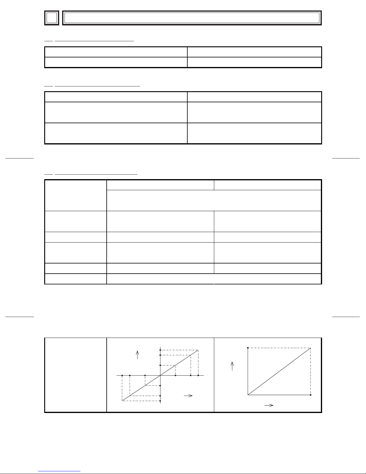
DEFINING GAIN AND OFFSET
(d)
(e)
(f)
Digital
Offset value
1000
(a)
Digital
(b)
(c)
〈〈
〈GAIN
〈〈
〉〉
〉
〉〉
Analog
Gain value
Gain is the angle or slope of the calibration line
identified at a digital value of 1000.
(a) Large gain– low reading resolution
(b) Zero gain-– default 5V or 20mA
(c) Small gain – high reading resolution
〈〈
〈OFFSET
〈〈
〉〉
〉
〉〉
Analog
Digital value 0
Offset is the 'Potion' of the calibrated line, identified
at a digital value of 0.
(d) Positive offset
(e) Zero offset – default (4-20mA default is 4mA)
f
( ) Negative offset
Offset and gain can be used independently or together. Reasonable offset ranges are -5V to +5V or
-20mA to 20mA, and gain-offset difference 1V to 15V or 4mA to 32mA. Gain and offset can be adjusted by
software in the FX base unit (see program example 2) or by the switches on the FX-2DA (with the aid of a
voltmeter/ammeter).
●
Bit device's b0, b1 of the gain/offset BFM (#21) should be set to 0, 1 to allow adjustment.
Once adjustment is complete these bit device should be set to 1, 0 to prohibit any further changes.
●
Channel initialization (BFM #0) should be set to the nearest range, i. e. voltage/current etc.
1. Power up the system the FX base unit can be in either RUN or STOP mode.
2. Connect the load and voltmeter or ammeter to the CH1 terminals.
3. Set the FX-2DA MODE switch to output CH1.
4. Press the OFFSET button once. The offset value is output. Use the UP/DOWN switch to reach the desired
offset value.
5. Press the GAIN button once. The gain value is output. Use the UP/DOWN switch to reach the desired
offset value.
6. Repeat operations 3 to 5 for each channel you wish to use.
7. Set the FX-2DA MODE switch to READY to complete gain and offset adjustment.
NOTE : If the MODE switch is not set to a channel number, the FX-2DA is regarded as being in the
READY status and no adjustments can be made.

5 EXAMPLE PROGRAM
5.1 Basic program
In the following example, channel CH1 is set to voltage output, while CH2 is set to current output. The FX2DA unit is connected at the position of special function block No.1. If the programmable controller is
changed to the STOP mode, the last data sent will remain and the outputs will hold.
M8000
RUN
monitor
M1
FROM(P)
●
Set CH1 setting to D0
●
Set CH2 setting to D1
TO
K1
CMP
K1
K3010
K30
(-2,000 to +2,000)
( 0 to +1,000)
K1
D4
D4
D0
K1
M0
K1H10K0K1TO(P)
K2
The ID code for the special function block at position
“1”is read from BFM #30 of that block and stored at
D4 in the FX base unit. This is compared to check the
block is an FX-2DA, if OK M1 is turned ON. These
two program steps are not strictly needed to perform
an analog output. They are however a useful check
and are recommended as good practice.
The analog output channels (CH1, CH2) are set up
by writing H10 to BFM #0 of the FX-2DA.
(D0 → BFM #1 (output to CH1))
(D1 → BFM #2 (output to CH2))
K4M10
FROM
NO
error
K1
M18M10
READY
K29
M20
Output
range
normal
K1
M3
The operational status of the FX-2DA is read from
BFM #29 and output as bit devices at the FX base
unit.
Output data normal

5.2 Using gain and offset in a program
I/O characteristics of the FX-2DA can be adjusted by changing the gain and offset parameters. These can
be changed by the switches of the FX-2DA with the aid of Voltage & Current meters or simply changed by
writting these settings from the programmable controller.
Only the gain and offset values in the memory of the FX-2DA need be adjusted. A voltmeter or an ammeter
for the analog output is not needed. A program for the programmable controller will be needed however.
The following is an example; changing the offset value to 0mA and gain value to 20mA on output channel
CH2 of the FX-2DA connected as block No.1.
Example: Adjusting gain/offset via software settings
X010
M0
TO(P)
K1
K0
H10
M0SET
K1
●
Adjustment start.
●
(H10) → BFM #0 (initialize input channels)
In the program shown at left, the programmable
controller should be in RUN status, and MODE
switch of the FX-2DA in the READY position.
TO(P)
K1
K21
K1
K1
●
(K1) → BFM #21
BFM #0 should be of HEX value H10, and (b1,
b0) of BFM #21 should be (0, 1).
T0
T1
TO(P)
TO(P)
TO(P)
TO(P)
K1
K1
K1
K1
K23
K24
K22
K21
K0
K20000
HC
RST
K2
K1K0K22K1TO
T0
K1
K1
K1
M0
K1
K4
●
(K0) → BFM #22 (offset/adjust)
Reset adjust bits.
●
(K0) → BFM #23 (offset)
This statement may be omitted if BFM #23 is already
at its default value.
●
(K20000) → BFM #24 (gain)
●
(HC) → BFM #22 (offset/gain set)
A delay of 300ms may be needed between setting
BFM #0 and #22 (see section 3.4“caution”)
●
Adjustment end.
●
(K2) → BFM #21
BFM #21 gain/offset adjust prohibit.

6
DIAGNOSTICS
6.1 Preliminary checks
1. Check whether the output wiring and/or expansion cables are properly connected on FX-2DA analog special
function block.
2. Check that the FX system configuration rules have not been broken, i.e. the number of blocks does not
exceed 8 and the total system I/O is equal or less than 256 I/O.
3. Ensure that the correct operating range has been selected for the application.
4. Check that the MODE switch on the FX-2DA panel is set to the READY position.
5. Check that there is no power overload on either the 5V or 24V power source, remember the loading on
the FX base unit or a powered extension unit varies according to the number of extension blocks or
special function blocks connected.
6. Pit the main processing unit into RUN.
6.2 Error checking
If the FX-2DA special function block does not seem to operate normally, check the following items.
●
Check the status of the POWER LED.
Lit. : The extension cable is properly connected.
Otherwise : Check the connection of the extension cable.
●
Check the external wiring.
●
Check the status of“24V”LED (top right cover of the FX-2DA).
Lit. : FX-2DA is OK, 24V DC power source is OK.
Otherwise : Possible 24V DC power failure, if OK then possible FX-2DA failure.
●
Check the status of th“D/A”LED (top right cover of the FX-2DA)
Lit. : D/A conversion is proceeding normally
Otherwise : Check buffer memory #29 (error status). If any bits (b2 and b3) are ON, then this is why the D/A LED
is OFF.

Guidelines for the safety of the user and protection of
the FX-2DA special function block
●
This manual has been written to be used by trained and competent personnel. This is defined
by the European directives for machinery, low voltage and EMC.
●
If in doubt at any stage during the installation of the FX-2DA always consult a professional
electrical engineer who is qualified and trained to the local and national standards. If in doubt
about the operation or use of the FX-2DA please consult the nearest Mitsubishi Electric distributor.
●
Under no circumstances will Mitsubishi Electric be liable or responsible for any consequential
damage that may arise as a result of the installation or use of this equipment.
●
All examples and diagrams shown in this manual are intended only as an aid to understanding
the text, not to guarantee operation. Mitsubishi Electric will accept no responsibility for actual
use of the product based on these illustrative examples.
JY992D52801C
Manual number : JY992D52801
Manual revision : C
Data : AUGUST 1996
HEAD OFFICE : MITSUBISHI DENKI BLDG MARUNOUCH TOKYO 100 TELEX : J24532 CABLE MELCO TOKYO
HIMEJI WORKS : 840, CHIYODA CHO, HIMEJI, JAPAN
Effective AUG. 1996
Specifications are subject
to change without notice.
 Loading...