MITSUBISHI<Dig.Ana.INTERFACE>
As applications for microcomputers are increasing,a desire has
arisen for a RAM backup function.Let us introduce Mitsubishi
Electric new low power dissipation,high-performance system
reset IC,which is suitable for such RAM backup.
The M62009,which is a low power-dissipation 2-output
microcomputer system reset IC,is a 2-output system reset IC
which provides for RAM backup in microcomputers,and
reduces power dissipation by using the Bi-CMOS process.The
M62009 considerably reduces the number of components in
the reset circuit.
The M62009 performs two-stage detection of normal supply
voltage and backup supply voltage required for backup
mode.When the supply voltage is switched from normal supply
voltage to back up supply voltage the interruption output,which
is one of the two outputs,gives the interruption signal to a
microcomputer,in this way,the microcomputer reduces power
dissipation and enters in the backup mode. If the backup
supply voltage goes lower than the voltage required for
backup,the reset output(RESET output)which is different from
the INT output gives the reset signal (forced reset) to the
microcomputer.The interruption signal from the INT output
recovers the microcomputer from the backup mode. To
recover from reset, RESET output is canceled when the
specified interval of time (delay time) elapses after the signal is
given from the INT output.
office,industrial,and home-use equipment.
1
M62009L,P,FP
LOW POWER 2 OUTPUT SYSTEM RESET IC WITH EXTERNAL INPUT
DESCRIPTION
FEATURES
•Bi-CMOS process low power dissipation circuit configuration
Icc=7µA(Typ.) (Normal mode Vcc1=Vcc2=5.0V)
Icc=5µA(Typ.) (Backup mode Vcc1=5.0V)
Icc=1µA(Typ.) (Backup mode Vcc1=2.5V)
•Two supply detection
Vcc1(RESET) Vcc1-1=4.0V(typ):Increase of Vcc1
Vs1-2=2.0V(typ):Decrease of Vcc1
Vcc2(INT) Free set up
•Two outputs(open drain type)
Reset output (RESET):Forced reset signal output
Interruption output(INT):Output of the signal for interruption
processing
(output of the switching signal for
backup mode)
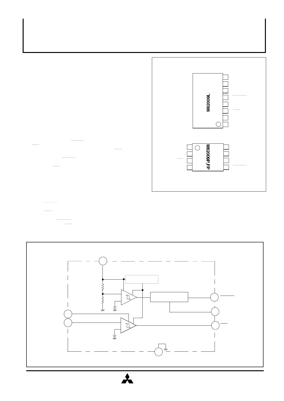
BLOCK DIAGRAM
Vcc1
7
Vs1-1 4.0V(TYP)DETECTION
Vs1-2 2.0V(TYP)DETECTION
PIN CONFIGURATION (TOP VIEW)
8
NC
7
Vcc1
6
Cd
5
RESET
4
GND
3
INT
2
Vcc2
1
VI
Outline 8P5(L)
8
1
VI
INT
GND
2
3
4
Outline 8P4(P)
8P2S-A(FP)
Vcc2
•Packages 2 types
5-pin SIP (single in-line)
8-pin SOP (mini flat)
NC
7
Vcc1
6
Cd
5
RESET
NC:NO CONNECTION
APPLICATION
Prevention of errors in microcomputer system in electronic
equipment that requires RAM backup,such as
Vcc2
VI
2
BIAS CIRCUIT
+
-
-
+
Vs2
1.25V(TYP)
MITSUBISHI
ELECTRIC
DELAY CIRCUIT
4
GND
5
6
3
RESET
Cd
INT
1
( / 3 )

MITSUBISHI<Dig.Ana.INTERFACE>
M62009L,P,FP
LOW POWER 2 OUTPUT SYSTEM RESET IC WITH EXTERNAL INPUT
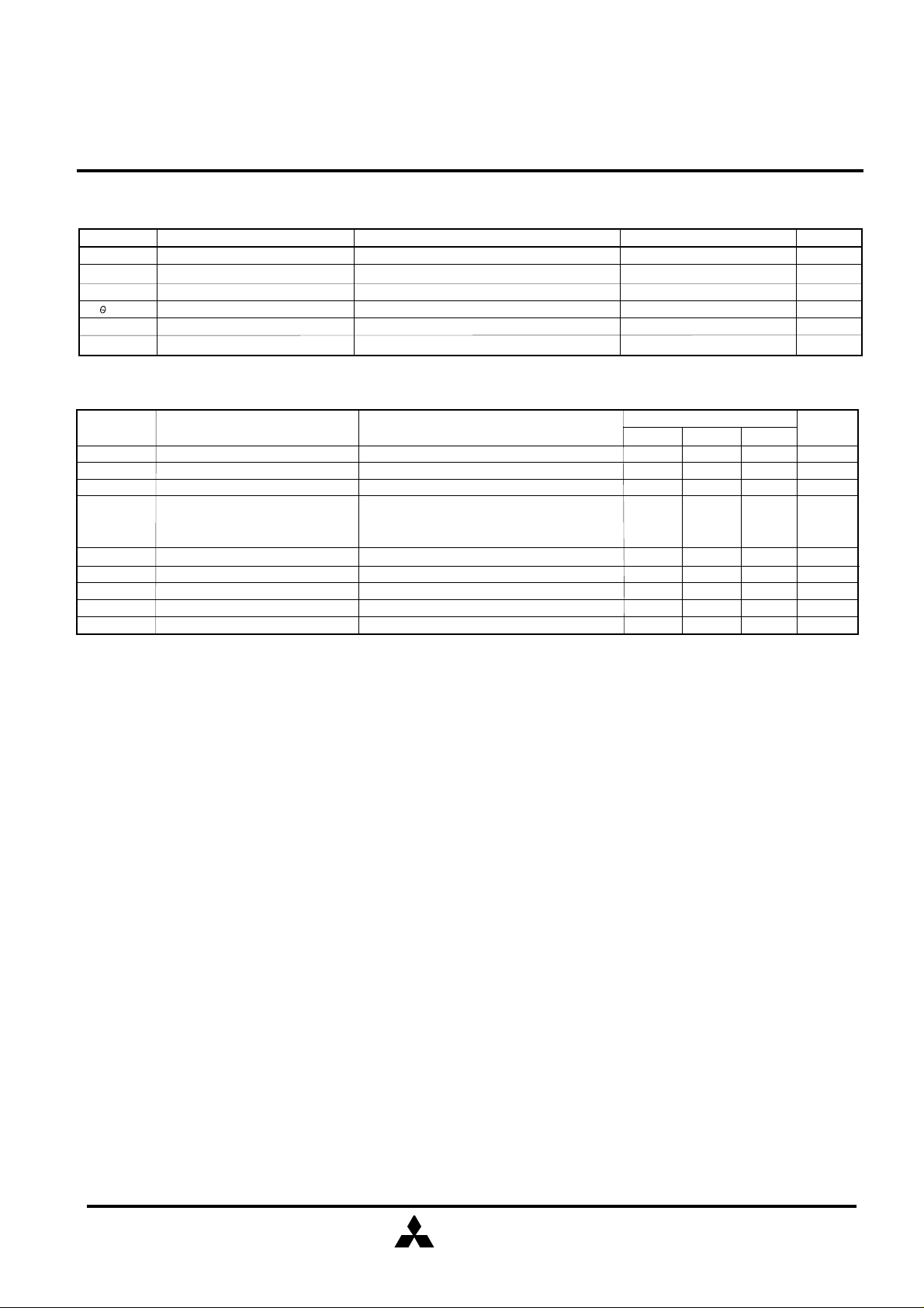
ABSOLUTE MAXIMUM RATINGS(Ta=25°C, unless otherwise noted)
Symbol Ratings
Vcc
ISINK
Pd
K
Topr
Tstg Storage temperature
Supply voltage
Output sink current
Power dissipation
Thermal derating
Operating temperature
Parameter
(Ta≥25°C)
ELECTRICAL CHARACTERISTICS(Ta=25°C, unless otherwise noted)
Symbol
Vs 1-1 Detection voltage
Vs 1-2
Vs 2
∆Vs
Detection voltage
Reference voltage
Hysteresis voltage
Parameter
Increase of Vcc1
Decrease of Vcc1
Decrease of VI
Vcc2=Detection voltage of hysteresis voltage
(Detection voltage=4V set up)
Conditions
Test conditions
800(SIP)/625(DIP)/440(FP)
8(SIP)/6.25(DIP)/4.4(FP)
-20 ~ +75
-55 ~ +125
Min.
3.8
1.85
1.20 1.30
8
5
Limits
Typ.
4.0
2.00
1.25
87
Max.
4.2
2.15
Unit
V
mA
mW
mW/°C
°C
°C
Unit
V
V
V
mV
ICC
ICC2-1
ICC2-2
td
Vsat
Circuit Current
Circuit Current
Circuit Current
Delay time
Output saturation voltage
Vcc1=Vcc2=5V
Vcc1=5V
Vcc1=2.5V
Cd=0.33µF
VIN=5V Ic=4mA(NMOS)
Vcc2=0V
Vcc2=0V
50
0.2
7
5
1
30
20
4.5
0.4
µA
µA
µA
mS
V
MITSUBISHI
ELECTRIC
2
( / 3 )

MITSUBISHI<Dig.Ana.INTERFACE>
5
M62009L,P,FP
LOW POWER 2 OUTPUT SYSTEM RESET IC WITH EXTERNAL INPUT
TIMING CHART
VSH
VSH
Vcc2
INT
1
Vs1-1
Vcc1
td td
RESET
1 Vcc2=VSH(Increase of Vcc2)INT output Low
2 Vcc2=VSL(Decrease of Vcc2)INT output High
3 Delay time obtained from Vs1-1.td=50msec(Cd=0.33µF):td=1.52X10 XCd(sec)
RESET output:reset cancel(cancel)
4 Vcc1=VS1-2(Vcc1 Decrease)
RESET output:forced reset output(L reset)
VSL
2
1
VSL
2
Vs1-2
43
VSH
1
Vs1-1
VSL
2
Vs1-2
3
4
APPLICATION CIRCUIT EXAMPLE
SUPPLY VOLTAGE
5.6V
BACKUP
CAPACITOR
SMOOTHING
CAPACITOR
MICROCOMPUTER SYSTEM RESET IC
Vcc2
VI
VDD
Vcc1
RESET
RESET
INT
INT
Cd
DELAY
CAPACITOR
Cd
MICROCOMPUTER
MITSUBISHI
ELECTRIC
( / 3 )
3
 Loading...