

Page 1
TENTATIVE
New Product
New Product
TENTATIVE
GENERAL PURPOSE BATTERY CHARGER CONTROL IC
Notice: This is not a final specification.
Some parametric limits are subject to change.
DESCRIPTION
The M62255FP is intended to be used a general purpose
battery charger control for Note PC. The M62255FP contains the
functions which are required for the battery charge control ,on
single chip using low peripheral component requirement . The
M62255FP can handle battery charge control, monitor battery
temperature and prevent from over current and voltage with
microcomputer. It contains DC-DC converter circuit which can
be used for the feedback control of the charge current and the
output voltage.
It is the best fit for Smart Battery Charger.
FEATURES
•Built-in 3 wire serial data interface for MCU.
•Built-in multiplexer and level magnification circuit with 4 input ports.
•Built-in DC-DC converter circuit for PWM function
•Built-in two current detection circuits. These circuits can detect
charge current and discharge current
•ON/OFF control with low power dissipation mode. (Power save)
MITSUBISHI<Dig./Ana. INTERFACE>
M62255FP
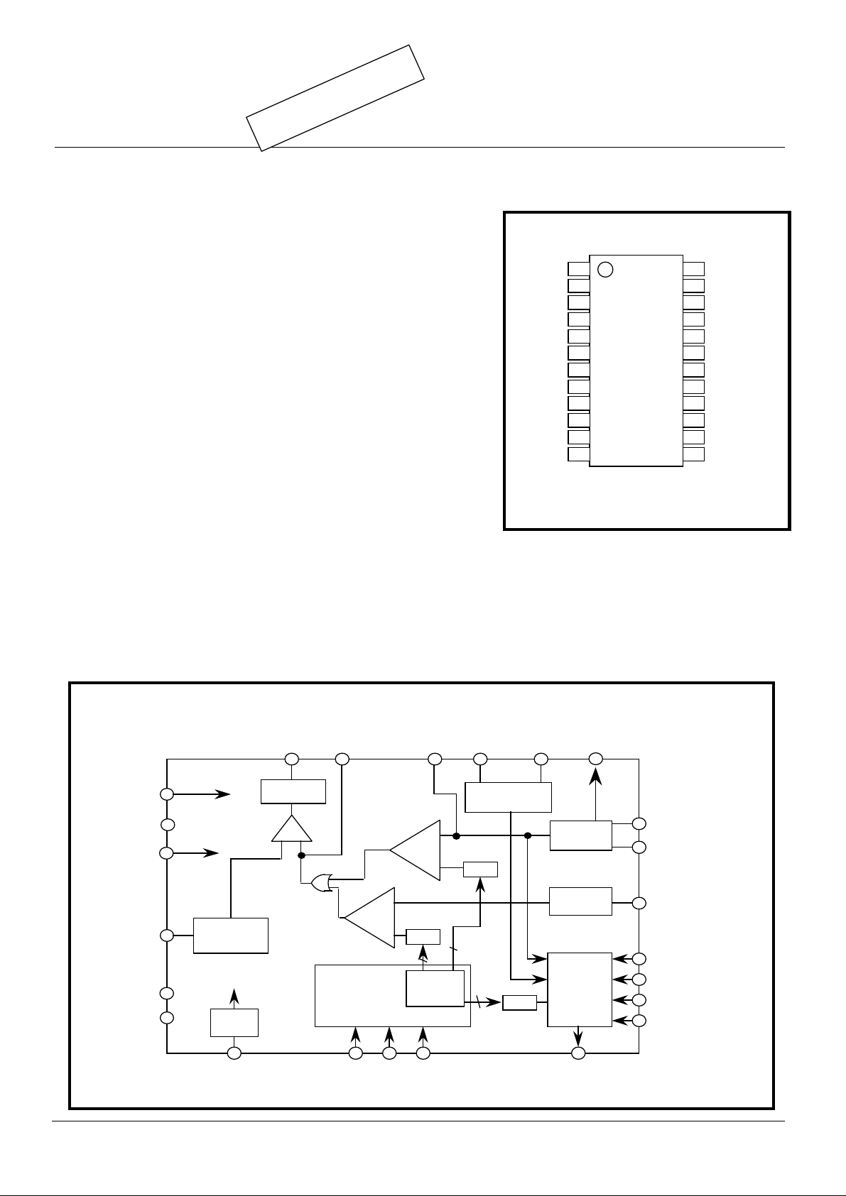
PIN CONFIGURATION (TOP VIEW)
SW
PGND
OSC
GND
PS
CK
DI
CS
DCDOUT
REF IN
ADJ
Vcc
1
2
3
4
5
6
7
8
9
10
11
12
M62255FP
24P2Q-A
24
23
22
21
20
19
18
17
16
15
14
13
Vc
VDET
IDET
ISENSE1 -
ISENSE1 +
IN1
IN2
IN3
IN4
DOUT
ISENSE2 -
ISENSE2 +
APPLICATION
Note.P.C, Video camera and general battery charger for other
digital equipment
BLOCK DIAGRAM
Vcc
ADJ
REF IN
OSC
PGND
GND
SW
Output
Drive circuit
PWM
Comp
OSC
To Internal Circuit
Power
Save
Vc
Voltage
control
OPAmp
IDET
Current
control
OPAmp
Vref
8bit
D-A
Converter
Logic Circuit
ISENSE2 -ISENSE2 +
Discharge Current
Detect Circuit
Vref
3bit
Vref
4bit
DCDOUT
Charge Current
Detect Circuit
Output Voltage
Detect Circuit
Multiplexer
&
Level
Magnification
Circuit
ISENSE1 +
ISENSE1 -
VDET
IN1
IN2
IN3
IN4
PS
CK DI DOUT
CS
( / 12 )
1
Page 2

TENTATIVE
New Product
New Product
TENTATIVE
<DESCRIPTION OF TERMINALS>
MITSUBISHI<Dig./Ana. INTERFACE>
M62255FP
GENERAL PURPOSE BATTERY CHARGER CONTROL IC
Pin No. Symbol
7
6
8
15
11
10
19
18
17
16
20
21
13
14
9
DI
CK
CS
DOUT
ADJ
REF IN
IN1
IN2
IN3
IN4
ISENSE1+
ISENSE1-
ISENSE2+
ISENSE2-
DCDOUT
Function
The serial data input pin which used to receive 8-Bit wide serial data
The shift clock input pin which input signal from DI pin to 8-Bit shift register by the
rising edge of clock signal
When this pin is "Low", DI pin can receive the data into the 8-Bit shift register.
The each bit will be latched at rising edge of the clock signal
The output pin of the amplified A-D data
The voltage output pin for adjusting A-D reference voltage
The reference voltage input pin of the A-D converter
The A-D converter input pin
The A-D converter input pin
The A-D converter input pin
The A-D converter input pin
The charge current sense input pin for high side voltage
The charge current sense input pin for low side voltage
The discharge current sense input pin for high side voltage
The discharge current sense input pin for low side voltage
The discharge current detect circuit output pin
23
22
24
1
3
5
12
4
3
VDET
IDET
VC
SW
OSC
PS
Vcc
GND
PGND
The voltage detection input pin
The current detection input pin
This pin is used to make connection with capacitor and resistor which
are used for phase compensation
The pre-drive pin which used to connect the external Pch Tr
The pin used to connect capacitor to determine the frequency of ocelot
The control pin of power save mode (H : power save mode, L : normal mode)
The power supply pin
The ground pin
The ground pin of power unit
( / 12 )
2
Page 3
TENTATIVE
New Product
New Product
TENTATIVE
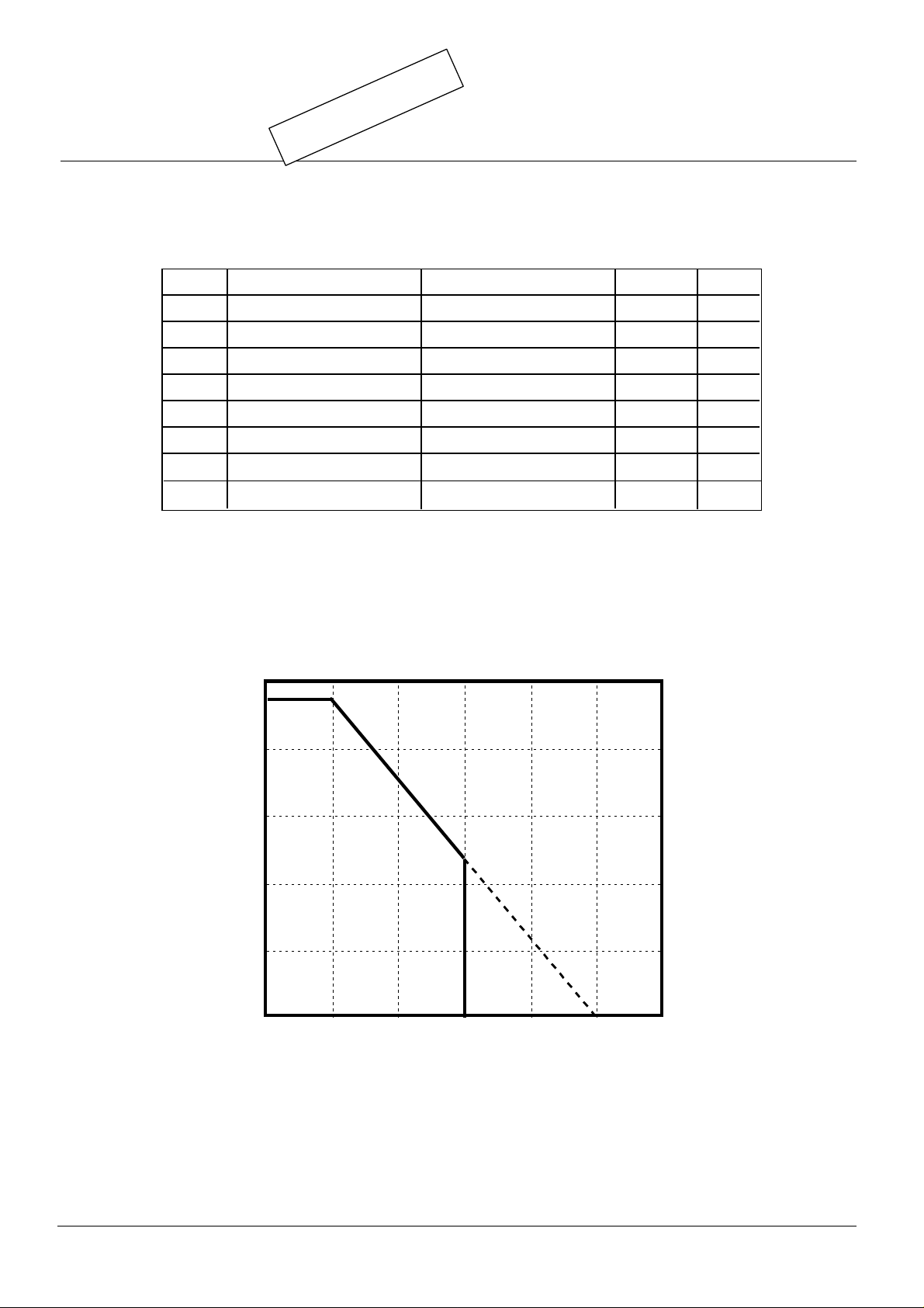
<ABSOLUTE MAXIMUM RATINGS>
MITSUBISHI<Dig./Ana. INTERFACE>
M62255FP
GENERAL PURPOSE BATTERY CHARGER CONTROL IC
Symbol Conditions
Vcc
Isw
Vsw
VPS
Pd
KTHETER
Topr
Tstg
Parameter
Supply voltage
SW drive current
SW max. voltage
PS max. voltage
Power dissipation
Thermal derating ratio
Operating temperature
Storage temperature
Ta=25°C
Ta>25°C
THERMAL DERATING (MAXIMUM RATING)
1000
950
Ratings
28
50
Vcc
7
950
9.5
-20 – +75
-40 – +125
Unit
V
mA
V
V
mW
mW/ °C
°C
°C
800
600
400
200
POWER DISSIPATION Pd (mW)
0
0 25 50 75 100 125
AMBIENT TEMPERATURE Ta (°C )
( / 12 )
3
Page 4
New Product
New Product
TENTATIVE
TENTATIVE
MITSUBISHI<Dig./Ana. INTERFACE>
M62255FP
GENERAL PURPOSE BATTERY CHARGER CONTROL IC
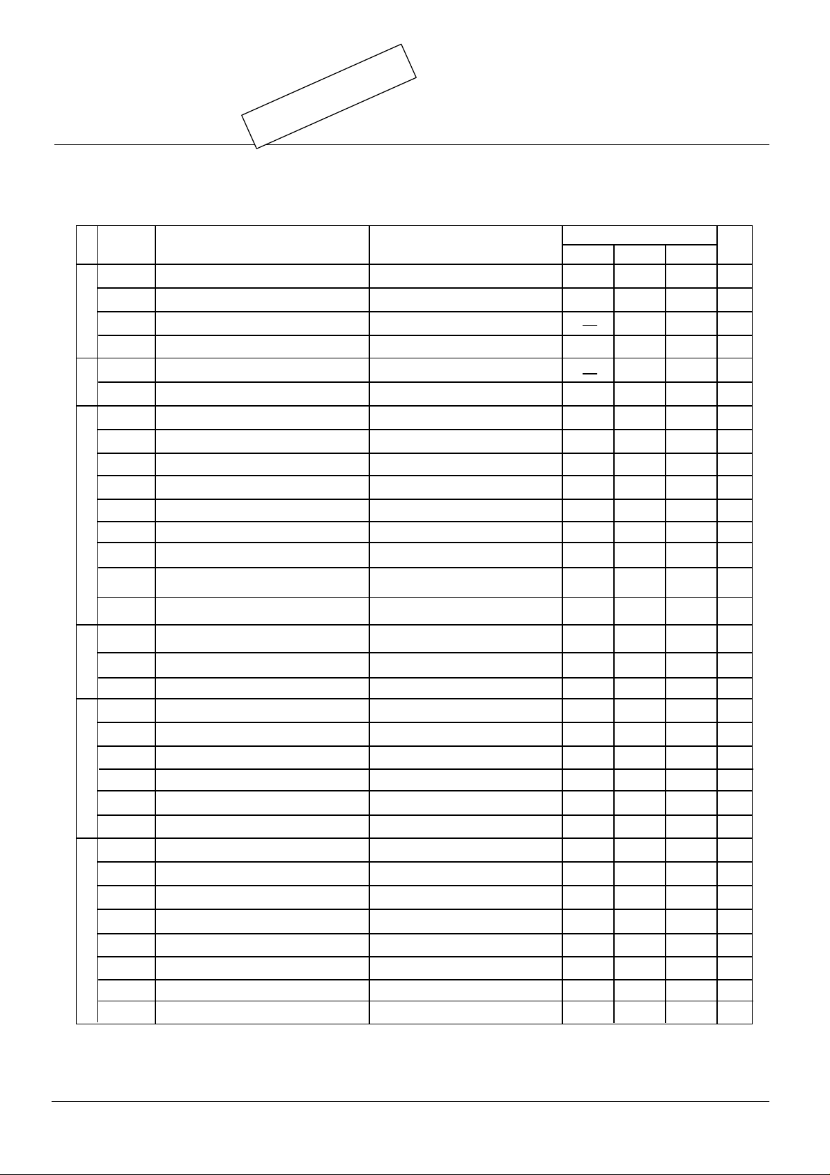
<ELECTRICAL CHARACTERISTICS>
Symbol Unit
Block
Vcc
Icc1
All block
Vref Input reference voltage
ISWL
PWM
VDET-IN
IDETB
VISENSE1+
VISENSE1- ISENSE1- input voltage range
VISENSE2+
VISENSE2-
VCH Charge voltage of fixed voltage
Charge detection block
VICH
DNL
Supply voltage
Circuit current
Circuit current at power saveIcc2
Main-SW output saturation voltageVsatM
SW output leak current
VDET input voltage range
VDET input bias current
ISENSE1+ input voltage range
ISENSE2+ input voltage range
ISENSE2- input voltage range
Charge current detection voltage of
fixed current
Differential nonlinearity at 8 bit DAC
PS input voltage VPS=2.0v
Isw=50mA
Vref=5.0v, Voltage control data is 4.2v
selected at Reset
Vref=5.0v, Current control data is
160mV selected
Vref=5.0v
(Ta=25°C, Vcc=15V)
Test conditionParameter
Limits
Min
Typ Max
7.5
4.0
7.0
50
5.0
0.9
-1 1
0.6
-1
2.0
2.0
2.0
2.0
Vcc-0.5
Vcc-0.5
Vcc+1.5
Vcc+1.5
4.20
160
-1
22
10.0
80
1.2
5.0
0
4.224.18
180140
1 LSB
V
mA
µA
V
V
µA
µA
µA
V
V
V
V
V
mV
VIN-IN
IIN
Level Mag.
VDOUT
fosc
Ioscch
Ioscdis
OSC
TDUTY Maxmum ON duty
Vosch
Voscl
V DIH
V DIL
V CSH
V CSL
IN input voltage range
IN input current
DOUT output voltage range
Oscillation frequency
Oscillation charge current
Oscillation discharge current
Oscillation output high level
Oscillation output low level
DI input high level
DI input low level
CS input high level
CS input low level
V CKH CK input high level
Inter Face
V CKL CK input low level
V PSH
V PSL
PS input high level
PS input low level
Cosc = 390pF
0.3
-100
0.5
70 130
-150
100
-120
20 30 40
95
0.85
0.35
0.95
0.4
1.05
0.45
3.5
0
3.5
0
3.5
0
1.0
1.5 V
0
5
0
5
KHz
-90
6.0
0.5
6.0
0.5
6.0
0.5
0.3 V
V
nA
V
µA
µA
%
V
V
V
V
V
V
V
V
4
( / 12 )
Page 5
TENTATIVE
New Product
New Product
TENTATIVE
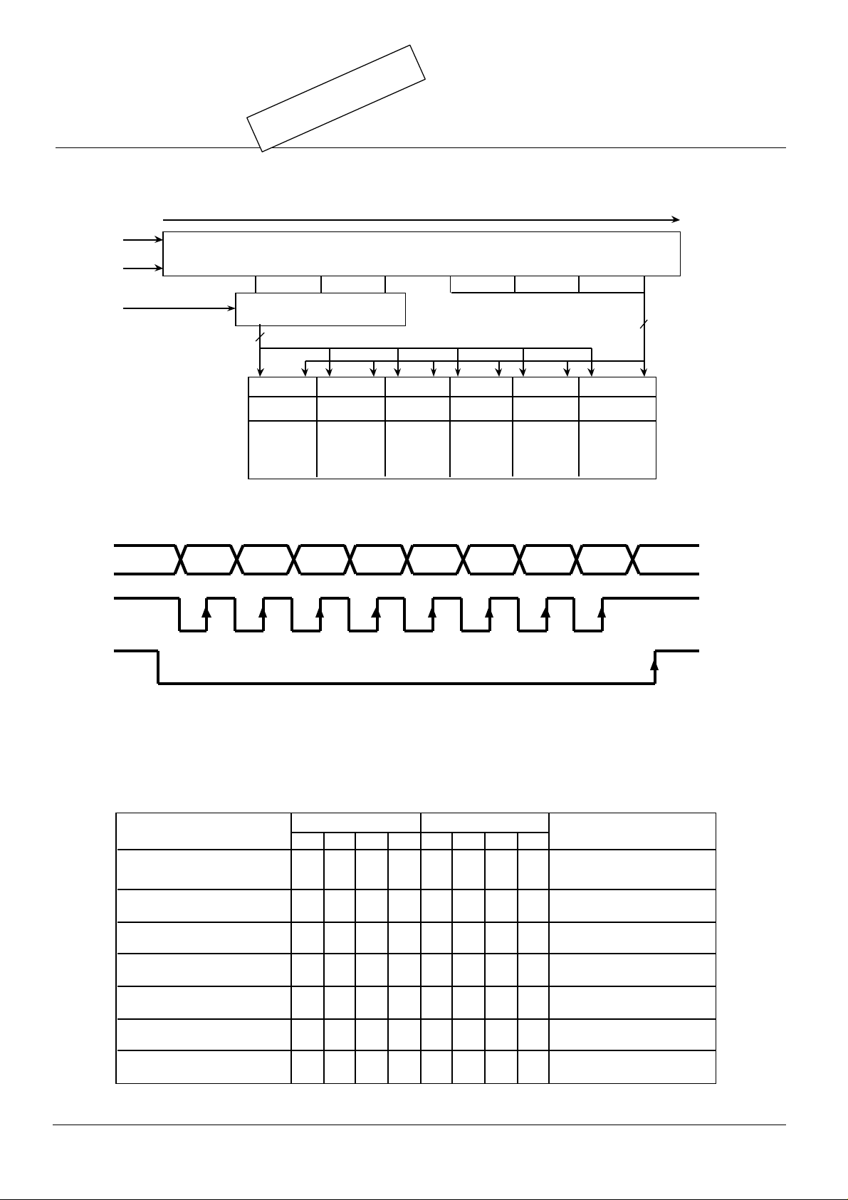
<DIGITAL DATA FORMAT>
MITSUBISHI<Dig./Ana. INTERFACE>
M62255FP
GENERAL PURPOSE BATTERY CHARGER CONTROL IC
MSB LSB
DI
CK
CS
D7 D6 D5 D4 D3 D2 D1 D0
ADDRESS DECODER
6
MPX MPX MPX MPX MPX MPX
CURRENT
CONTROL
SW
8-BIT SHIFT RESISTER
LATCH LATCH LATCH LATCHLATCHLATCH
VOLTAGE
CONTROL
SW
VOLTAGE
Fine
CONTROL
SW
AMP
SELECT
INPUT
SELECT
4
A-D
REFERENCE
SELECT
<DATA TIMING CHART > (MODEL)
DI
CK
LSB
D0 D1 D2 D3 D4 D5 D6 D7
MSB
FirstLast
CS
<DATA SETTING>
Control function
RESET
Current control
Voltage control
Voltage fine control
Amp. select
A-D Input select
A-D Reference select
Address Data
D6 D5 D4 D3 D2 D1 D0
D7
0
0
0
0
-
0
0
0
1
-
0
0
1
0
-
0
0
1
1
-
0
1
0
0
-
0
1
0
1
-
0
1
1
0
-
Description
A-D Reference voltage = 2.5V
-
-
-
-
-
-
-
-
-
-
-
-
-
- -
Voltage control setting = 4.2V
-
Voltage fine control setting = 0V
Current control setting = 20mV
See Table 1
-
-
See Table 2
-
See Table 3
-
See Table 4
-
See Table 5
See Table 6
( / 12 )
5
Page 6
New Product
New Product
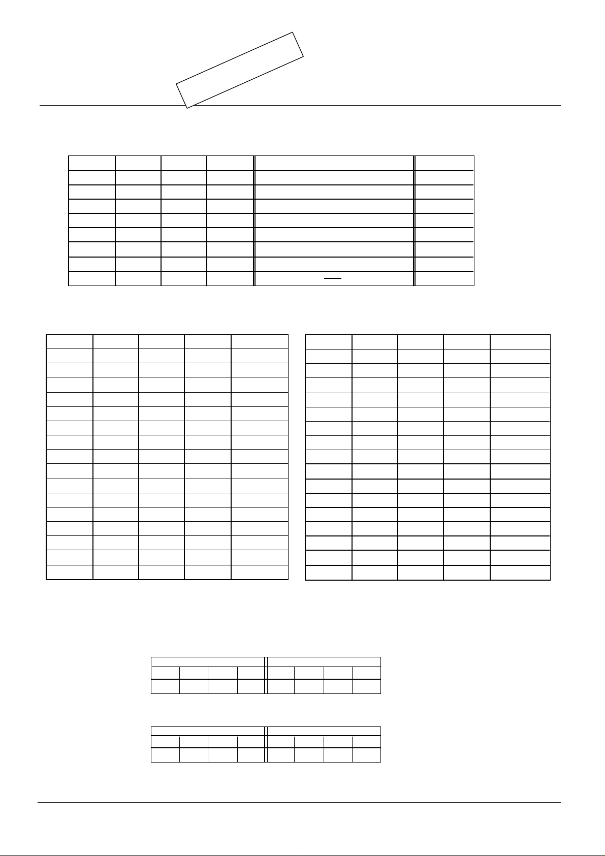
<CONTROL DATA>
Table 1 ; Current control data
TENTATIVE
TENTATIVE
MITSUBISHI<Dig./Ana. INTERFACE>
M62255FP
GENERAL PURPOSE BATTERY CHARGER CONTROL IC
D3 D2
0
0
0
0
0
0
0
0
• 20mV selected at RESET
0
0
0
0
1
1
1
1
Table 2 ;Voltage control data
0
0
0
0
0
0
0
0
1
1
1
1
1
1
1
1
• 4.20V selected at RESET
0
0
0
0
1
1
1
1
0
0
0
0
1
1
1
1
0
0
1
1
0
0
1
1
0
0
1
1
0
0
1
1
D1 D0 Current control input voltage
0
0
1
1
0
0
1
1
0
1
0
1
0
1
0
0V
20mV
40mV
80mV
160mV
240mV
320mV
1
Table 3 ;Voltage fine control data
D3 D2 D1 D0D3 D2 D1 D0 Ref.voltage
0
1
0
1
0
1
0
1
0
1
0
1
0
1
0
1
select 5.0V
select 4.84V
select 4.68V
select 4.52V
select 4.36V
select 4.20V
select 4.04V
select 3.88V
select 3.72V
select 3.56V
select 3.40V
select 3.24V
select 3.08V
select 2.92V
select 2.76V
select 2.60V
0
0
0
0
0
0
0
0
1
1
1
1
1
1
1
1
• 0V selected at RESET
0
0
0
0
1
1
1
1
0
0
0
0
1
1
1
1
Current ratio
0
1/16
1/8
1/4
1/2
3/4
1
Trickle
0
0
1
1
0
0
1
1
0
0
1
1
0
0
1
1
0
1
0
1
0
1
0
1
0
1
0
1
0
1
0
1
fine cntl.voltage
select 0V
select -10mV
select -20mV
select -30mV
select -40mV
select -50mV
select -60mV
select -70mV
select -80mV
select -90mV
select -100mV
select -110mV
select -120mV
select -130mV
select -140mV
select -150mV
• Set-up voltage of Voltage control is fixed by Ref. voltage (at Table2) and fine cntl. voltage (at Table3).
Set-up voltage of Voltage control can be fixed at 10mV step between 2.45V and 5.0V.
Example1.
Example2.
D3 D2 D1 D0
0 1 0 1 1 0 1 0
D3 D2 D1 D0
1 0 0 1 1 1 1 1
table 1 table 2
D3 D2 D1 D0
Set-up voltage;
4.20V(Ref. voltage) - 100mV(fine cntl. voltage) = 4.10V
table 1 table 2
D3 D2 D1 D0
Set-up voltage;
3.56V(Ref. voltage) - 150mV(fine cntl. voltage) = 3.41V
( / 12 )
6
Page 7
New Product
New Product
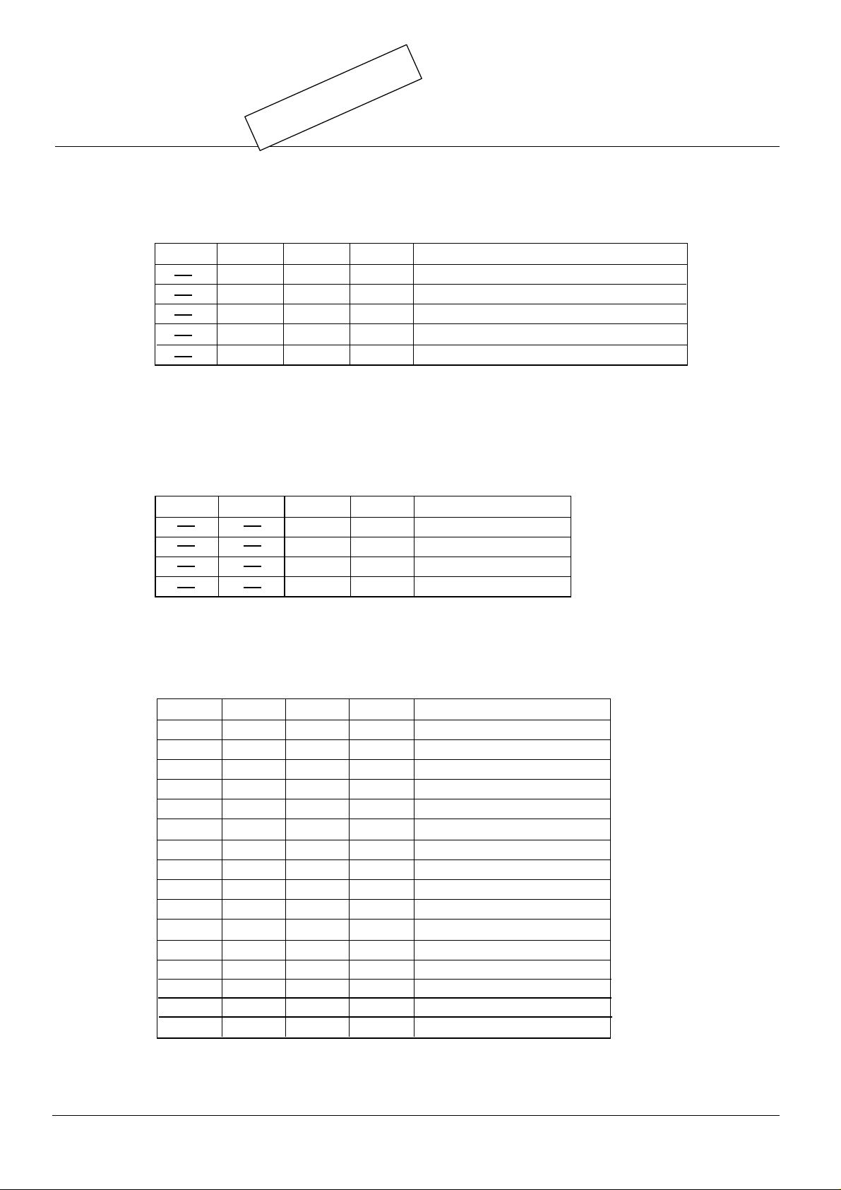
Table 4; Amp select
TENTATIVE
TENTATIVE
MITSUBISHI<Dig./Ana. INTERFACE>
M62255FP
GENERAL PURPOSE BATTERY CHARGER CONTROL IC
0
0
0
0
1
• Output of Battery Voltage Detect Amp is selected at RESET
Table 5; A-D Input select
D3 D2
• IN1 is selected at RESET
D1 D0D3 D2
0
0
1
1
0
D1
0
0
1
1
0
1
0
1
0
D0
0
1
0
1
State
select Output of Charge Current Detect Amp
select Input of Battery Voltage Detect Amp
select Output of Battery Voltage Detect Amp
select Output of Discharge Current Detect Amp
select Output of A/D reference Voltage
State
select IN1
select IN2
select IN3
select IN4
Table 6; A-D Reference voltage select
D3 D2 D1
0
0
0
0
0
0
0
0
1
1
1
1
1
1
1
1
• 2.50V is selected at RESET
0
0
0
0
1
1
1
1
0
0
0
0
1
1
1
1
0
0
1
1
0
0
1
1
0
0
1
1
0
0
1
1
D0
0
1
0
1
0
1
0
1
0
1
0
1
0
1
0
1
State
select 5.0V
select 4.69V
select 4.38V
select 4.06V
select 3.75V
select 3.44V
select 3.13V
select 2.81V
select 2.50V
select 2.19V
select 1.88V
select 1.56V
select 1.25V
select 0.94V
select 0.63V
select 0.31V
( / 12 )
7
Page 8
TENTATIVE
New Product
New Product
TENTATIVE
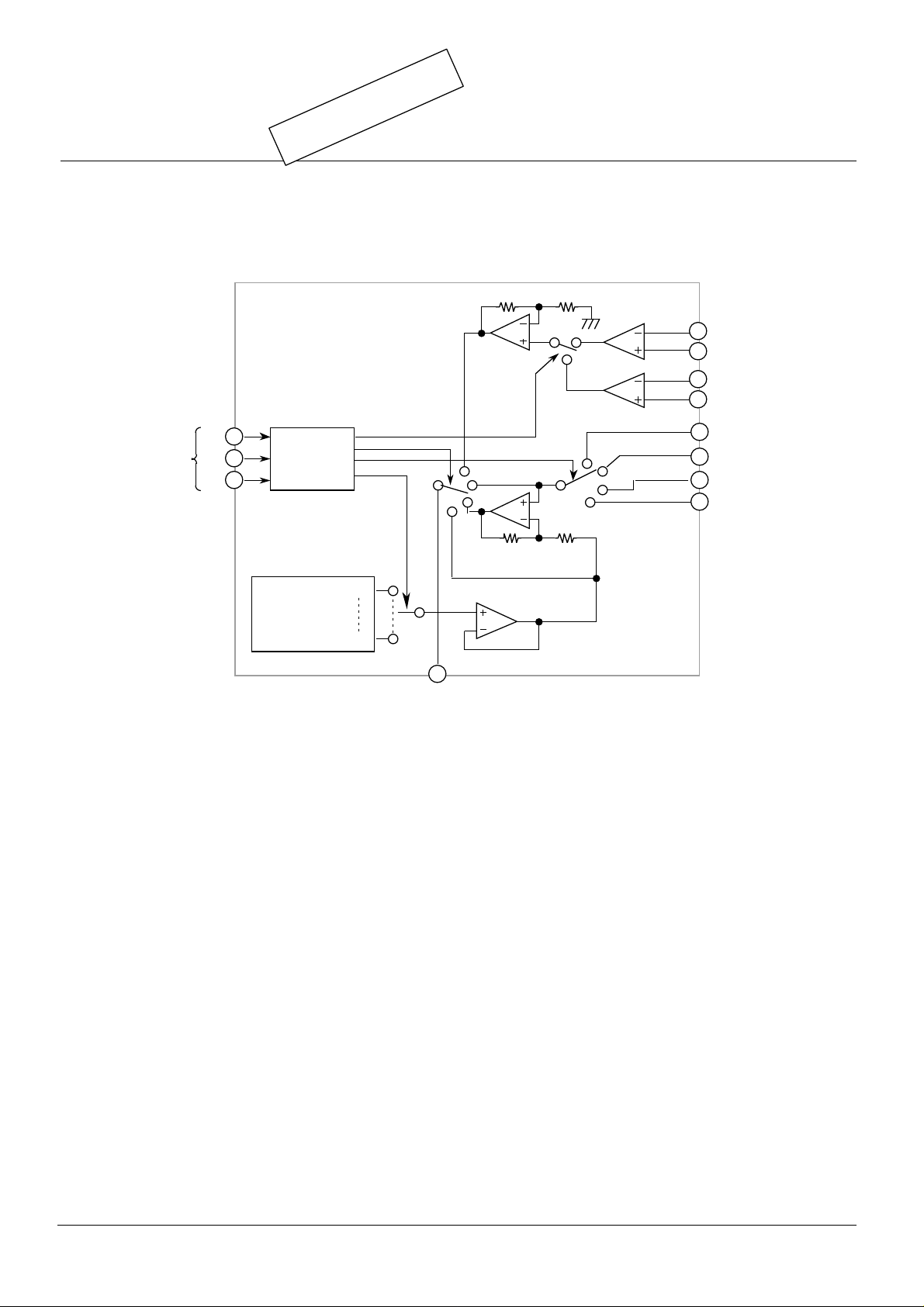
BLOCK DESCRIPTION
(1) Battery Voltage Detect BLOCK
MITSUBISHI<Dig./Ana. INTERFACE>
M62255FP
GENERAL PURPOSE BATTERY CHARGER CONTROL IC
1 1
Serial Data
from MCU
DI
CK
CS
Serial-Parallel
Converter
Circuit
3 1
5.0V
Reference
Voltage for
A-D Converter
0.31V
DOUT
to A-D input of MCU
Fig.1 Block Diagram of Multiplexer and Level Magnification Circuit
x10
x10
ISENSE2 -
ISENSE2+
ISENSE1 -
ISENSE1+
IN1
IN2
IN3
IN4
Multiplexer and Level Magnification Circuit of M62255 consists from Reference Voltage, 4times amplifier,
10times Amplifier and 4input Multiplexer.
When setting the reference voltage correspond to detecting voltage by serial data from MCU, this set
voltage supply to reference voltage for A-D converter. The difference between input voltage of IN1 - IN4
and reference voltage is multiplied by 4 at the center of this setting voltage.
This multiplied voltage is supplied to A-D input of MCU from DOUT terminal. The resolution of A-D
converter of MCU is improved by 2-Bit as against the difference of IN1-IN4 input.
( / 12 )
8
Page 9
New Product
New Product
4.9V
TENTATIVE
TENTATIVE
MITSUBISHI<Dig./Ana. INTERFACE>
M62255FP
GENERAL PURPOSE BATTERY CHARGER CONTROL IC
3.7V
To DOUT
To DOUT
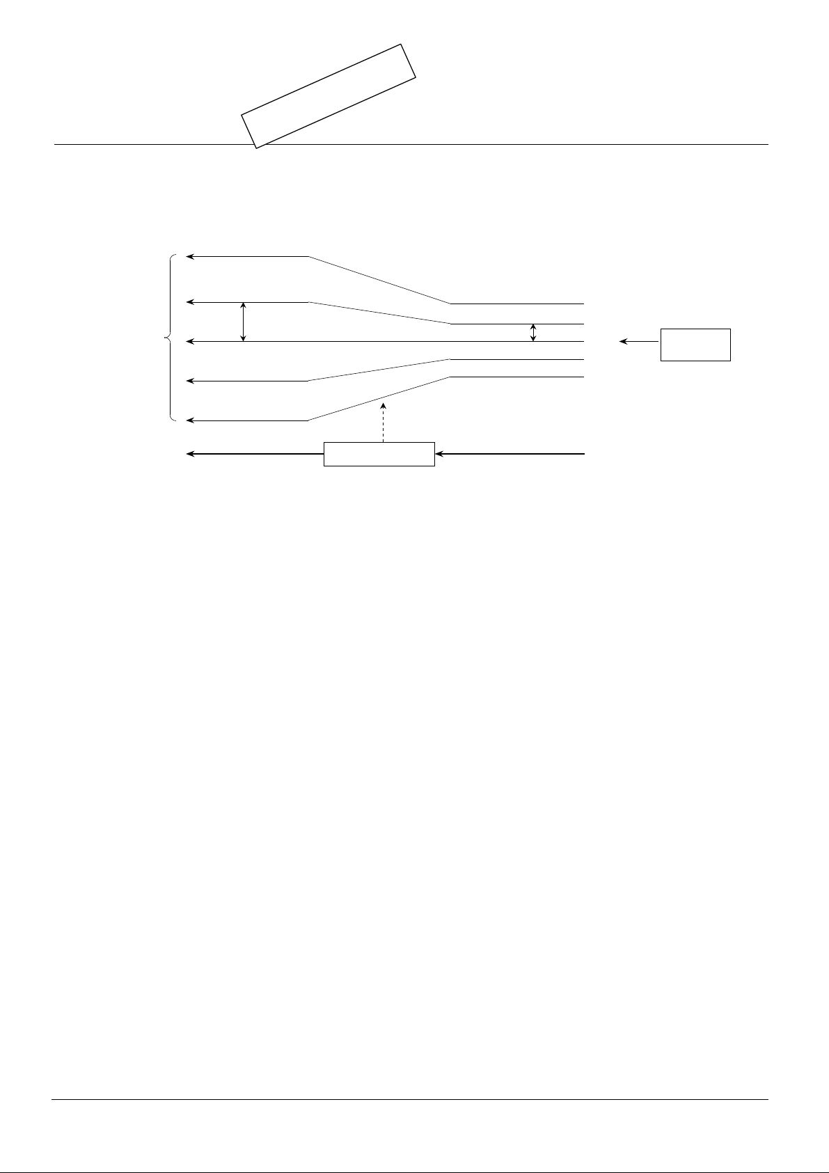
Output voltage of DOUT is fixed as follows;
VDOUT = (VIN - Vref) x 4 + Vref (V) ---------------- (1)
VDout ; Output voltage of DOUT
VIN ; Voltage of IN1 (or IN2,IN3,IN4)
Vref ; Reference voltage for A-D converter
In Fig.2 Reference Voltage is 2.5V. When Input voltage of IN1 (or IN2,IN3,IN4) is set at
2.8V, the difference between input voltage and Reference Voltage is 0.3V. The difference
voltage (0.3V) multiplied by 4 is 1.2V. 1.2V added to Reference Voltage(2.5V) makes
3.7V which is output voltage of VDOUT.
The range of output voltage of VDOUT is between 0V and 5V. So in Fig.2 the range of input
voltage of IN1(or IN2,IN3,IN4) is between 1.9V and 3.1V. (This range of input voltage is
difference from selected Reference Voltage.)
2.5V
1.3V
0.1V
1.2V
0.3V
4times Amplifier
Fig.2 Description of Level Magnification
3.1V
2.8V
2.5V
2.2V
1.9V
input voltage
Reference
Voltage
( / 12 )
9
Page 10
New Product
New Product
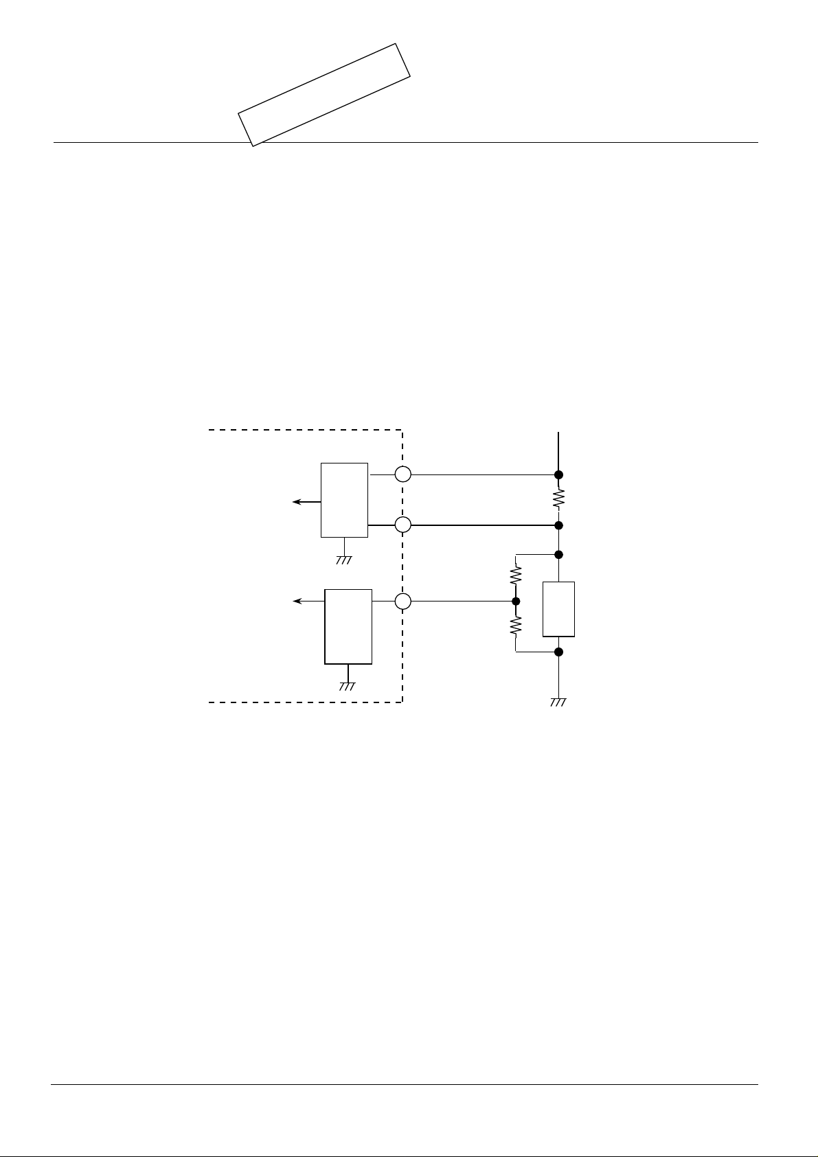
Charge Current of Current Detect R is multiplied by 10 and outputted from DOUT.
M62255 is for the floating detection type. Current Detect R is connected to + terminal
of battery.So M62255 is best fit for SMBus system ,because the common GND can
be given between PC system and the charger circuit.
Discharge current is detected by the same method as charge current.Detecting
discharge current can be used for monitoring the current consumption and the
remnant of the battery.
TENTATIVE
TENTATIVE
MITSUBISHI<Dig./Ana. INTERFACE>
M62255FP
GENERAL PURPOSE BATTERY CHARGER CONTROL IC
To 10times Amplifier
To 4times Amplifier
Fig.3 Detector Circuit of Battery Voltage / Charge Current
Current
Detect
Circuit
Multiplexer
Circuit
ISENSE+
ISENSE -
IN1 - N4
Charge Current
Detect R
Battery
( / 12 )
10
Page 11
New Product
New Product
TENTATIVE
TENTATIVE
DchgSW
From MCU
MITSUBISHI<Dig./Ana. INTERFACE>
M62255FP
GENERAL PURPOSE BATTERY CHARGER CONTROL IC
ChgSW
600K
0.1
22µ
200K
0.022µ
100µ
0.1µ
Battery 1
VC
IDET
ISENSE1-
ISENSE1+
Battery 2
IN1
VDET
Battery 3
From
each
Battery
IN3
IN2
IN4
DOUT
CS
Battery 4
To MCU
3
SW A
100
0.1
TO System
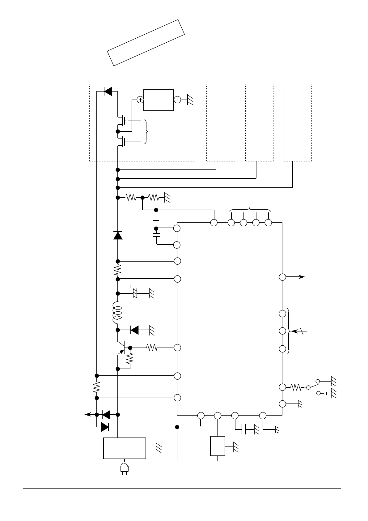
<Application Circuit>
AC
Adaptor
300
SW
ISENSE2+
( / 12 )
11
ISENSE2-
Vcc
M62255
REF IN
5V
Reg
OSC
390p
PGND
CK DI
PS
GND
150K
From MCU
Normal
5v
PS
Page 12

TENTATIVE
New Product
New Product
PACKAGE OUTLINE
TENTATIVE
MITSUBISHI<Dig./Ana. INTERFACE>
M62255FP
GENERAL PURPOSE BATTERY CHARGER CONTROL IC
( / 12 )
12
 Loading...