

DESCRIPTION
controller. Its functions are the driving and laser power
control of a specific type(Mitsubishi's N-type laser)of
semiconductor laser diode,in which the anode of a
semiconductor laser diode is connected in stem structure
to the cathode of a monitoring photodiode.
The IC has a laser drive current output pin of sink type
and is capable of driving a laser diode on a maximum bias
current of 40mA and a maximum switching current of 100
mA,which is switching at a rate of 200Mbps.
Since the M61880FP has a built in sample-hold circuit,it is
possible to realize an internal APC* system that requires
no external device for laser power control.
*:Automatic Power Control
The M61880FP is a semiconductor laser-diode driver/
MITSUBISHI < DIGITAL ASSP >
M61880FP
Laser-diode driver / controller
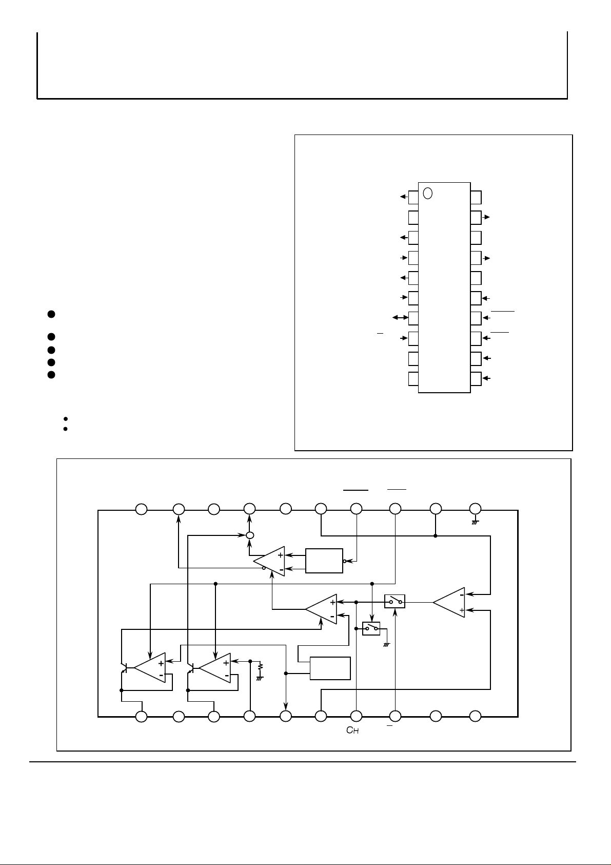
PIN CONFIGURATION (TOP VIEW)
FEATURES
Built-in sample-hold circuit for internal APC function
Hold error voltage is less than 1% for 1µs(C=0.047µF)
High speed switching 200Mbps
Large driving current 100mA (max)
Capable of setting bias current (40mA max)
5V single power supply
APPLICATION
Semiconductor laser-diode applied equipment
Laser beam printer(LBP)
Plain Paper Copier(PPC)
BLOCK DIAGRAM
OUTPUT TO SWITCHING
CURRENT SETTING LOAD
OUTPUT TO BIAS CURRENT
SETTING LOAD
BIAS CURRENT SETTING
VOLTAGE INPUT
REFERENCE VOLTAGE
OUTPUT
REFERENCE VOLTAGE
INPUT
HOLDING CAPACITOR
LOAD INPUT/OUTPUT
SAMPLE-HOLD
CONTROL INPUT
1
RS
RB
VB
Vr
Vcc1
NC
2
3
4
5
6
7
8
9
10
GND1
Vref
CH
S / H
Outline 20P2N-A
20
Vcc2
RO
N C
LD
GND2
PD
DATA
ENB
2RM
1RM
LASER CURRENT
LOAD OUTPUT
LASER CURRENT
OUTPUT
MONITORING
DIODE INPUT
SWITCHING
DATA INPUT
LASER CURRENT
ENABLE INPUT
MONITORING
LOAD INPUT 2
MONITORING
LOAD INPUT 1
19
18
17
16
15
14
13
12
11
NC : No connection
Vcc2 RO N C GND2 PD 2RM 1RM
181920
IB
1 2 3
GND1
RS RB VB Vref Vr Vcc1 NC
LD
17
+
4
16
ISW
50K
1.5V
5 6
1
( / )
TTL/ECL
2.5V
Reference
voltage
11
DATA
15
7
ENB
1314
8 9
12
11
COMP
10
S/H
MITSUBISHI < DIGITAL ASSP >
is not used.
bias current to LD independent of the state of the DATA input.
M61880FP
Laser-diode driver / controller
FUNCTIONS
The M61880 is a semiconductor laser-diode driver/controller.
Its functions are the driving and laser power control of a specific type (Mitsubishi's N type laser) of semiconductor laser
diode , in which the anode of a semiconductor laser diode
(LD) is connected in stem structure to the cathode of a monitoring photodiode (PD).
The functions to drive LD and to control laser power are carried out by connecting an external capacitor to the CH pin and
applying a reference voltage to the Vr pin.
The PD current generated by LD illumination flows through
the resistor connected between 1RM and 2RM , thereby gen-
PIN DESCRIPTIONS
Pin Name
LD
PD
Rs
RB
Laser current output Connect to cathode on semiconductor laser diode.
Monitoring diode input
Switching current
Set load output
Bias current
Set load output
Connect to anode on monitoring photodiode.
Connect a load resistor between this pin and GND for the setting of current (lsw)
to be switched.
Connect a load resistor between this pin and GND for the setting of bias current
(IB). Leave this pin open if IB is not used.
erating a potential difference (Vm). Vm is compared with the
voltage applied to the Vr pin. If Vm < Vr , a constant current is
sourced through the CH pin so that the external capacitor is
charged. If Vm > Vr , a constant current sinks through the CH
pin to discharge the external capacitor.
The above operation occurs when the S/H input is "L" and
DATA = "L" (sample).When the S/H input is "H" , the CH pin
is maintained at high impedance state (hold) , irrespective of
the state of Vm , Vr , and DATA input.
The LD drive current is made up of the switching current, lsw,
which is controlled by the DATA input, and IB , which is the
Description
VB
DATA
1RM,2RM
ENB
RO
S/H
CH
Vref
Vr
Vcc1 Power supply pin 1
Bias current setting
voltage input
Switching data input
For monitoring
Load input
Laser current enable input
Laser current load output
Sample hold control input
Holding capacitor load
input/output
Reference voltage output
Reference voltage input
Bias current (IB) is set by applying a voltage at this pin. Leave this pin open if I
If this pin is "L" ,a current of Isw+IB flows through laser diode, if "H" , current
IB flows.
A load resistor is connected between pins 1RM and 2RM for conversion of
current generated by monitoring photodiode into changes in voltage.
( 2RM pin connects to GND in the IC.)
If this pin is "H" all current source circuits are turned off.
Connect a laser current load resistor between this pin and Vcc.
If this pin is "L" ,sampling (APC) occurs, if "H" ,holding (switching).
Connect a holding capacitor between this pin and GND. Inside the M61880
Connect a holding capacitor between this pin and GND. Inside the M61880
this pin connects to the output of the sample-hold circuit and the current source
this pin connects to the output of the sample-hold circuit and the current source
input for Isw.
input for Isw.
Internal reference voltage (1.5Vtyp.) output pin of M61880.
A reference voltage is applied to this pin to operate the comparator in the
sample-hold circuit. Connect this pin to the Vref pin if the internal reference
voltage of the M61880 is to be used.
Power supply to internal analog circuits. Connect to a positive power source(+5V).
B
Vcc2
GND1
GND2
Power supply pin 2
GND pin 1
GND pin 2 GND for internal digital circuits.
Power supply to internal digital circuits. Connect to a positive power source(+5V).
GND for internal analog circuits.
2
11
( / )
OPERATION
1.Laser Drive Currents Setting Method
Laser Drive Current=Isw(switching current)+IB(bias current)
at switching mode
(1)Isw(Switching Current)
First it is necessary to decide the center value(Isw0) of
maximum switching current Isw(max).Isw0 is depend on
Rs ( load for switching current setting) by the following
equation.
(a)
Isw0 [mA] = 30 X
(b) When switching current is center value( Isw0) , it is
necessary to set up Rm ( load resistor for monitor of
photodiode current ) as follows:
VM(voltage across resistor Rm) = Vr (reference voltage )
at this condition CH pin voltage =2.5V.
When CH pin voltage < 2.5V , Isw <Isw0
When CH pin voltage > 2.5V , Isw >Isw0
(CH pin voltage changes from 2V to 3V at APC mode)
(c) The usable range of ISW at APC mode
That is 20 ~180% of Isw0 accurately.
(2) IB(Bias Current)
Bias current (IB) is set by RB (resistor for the setting of
bias current) and VB (voltage for the setting of bias current).
IB [A] = 1 X
1.2V ≤ VB ≤ Vcc-2.7V
IB(max.)=40mA
2.Switching Operation
If DATA = "L" , the LD drive current is Isw+IB
if DATA = "H" , IB.
3.ENB input
When the laser drive current is controlled by the DATA input,
the M61880's internal current source is maintained turned on.
In contrast, the control by ENB is turning on and off at the current source. If ENB = "L" the current source turns on ; if ENB
= "H" off.
When ENB = "H" the CH pin is compulsorily fixed to "L" in
order to discharge the capacitor connected to the CH pin.
Vref(1.5V) [V]
Rs [kΩ]
VB [V]
RB [Ω]
MITSUBISHI < DIGITAL ASSP >
M61880FP
Laser-diode driver / controller
4.Internal Reset Function
The M61880 has a reset circuit built in for the protection of
laser from an excessive current flowing at the moment of
power on. The internal current source goes off in the range
Vcc < 3.5V(typ.), and the CH pin is compulsorily fixed to "L"
at the same time.
5.RO Pin
A load resistor for laser drive current is connected to the RO
pin, through which a current almost equal to Isw flows in.
The load resistor is connected between the RO pin and Vcc
to reduce power dissipated in the IC.
Due to reasons related to the operation of circuits, the voltage
at this pin should be 2.5V or higher.
Consequently, the maximum resistance, RO(max.), of load resistor RO is :
RO(max.) [Ω] =
where Isw(max.) is the maximum of Isw. If, for example,
Vcc(min.)= 4.75V and Isw(max.)= 100mA, RO(max.)=22Ω.
Accordingly, if the resistance of RS is selected so as to gain
maximum Isw of 100mA, RO should be 22Ω at the maxi-
mum.
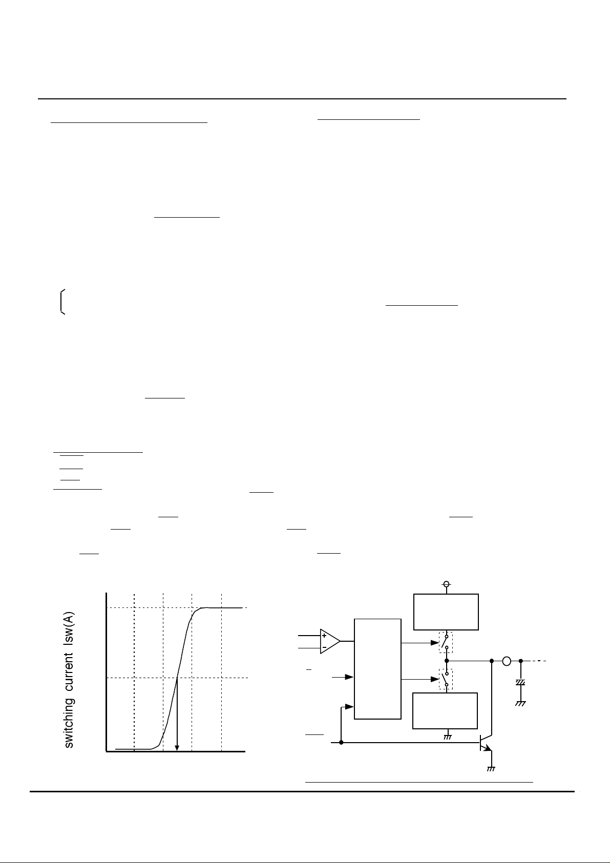
6.Sample-Hold Circuit
(1) Circuit Operation Overview
The following is an overview of the operation of the sample-
hold circuit contained in the M61880.
The PD current generated by LD illumination flows through
the resistor connected between 1RM and 2RM, thereby gen-
erating a potential difference(Vm). Vm is compared with the
voltage applied to the Vr pin. If Vm < Vr , a constant current is
sourced through the CH pin so that the external capacitor is
charged. If Vm > Vr , a constant current sinks through the CH
pin to discharge the external capacitor. This operation occurs
when the S/H input is "L" and DATA= "L" (sample).
When the S/H input is "H" , the CH pin is maintained at high
impedance state(hold), irrespective of the state of Vm, Vr, and
DATA input.
Vcc(min.) -2.5 [V]
Isw(max.) [mA]
2Isw0
Isw0
0
1.0
3.0
4.0
2.5
2.0
CH pin voltage VCH (V)
200%
100%
0%
( / )
Constant
Comparator
current source
for charging
Vr
Vm
SW1
Control
S / H
ENB
circuit
SW2
Constant
current source
for discharging
Conceptual Diagram: sample-hold circuit
11
3
Output
CH
External
capacitor
Tr1
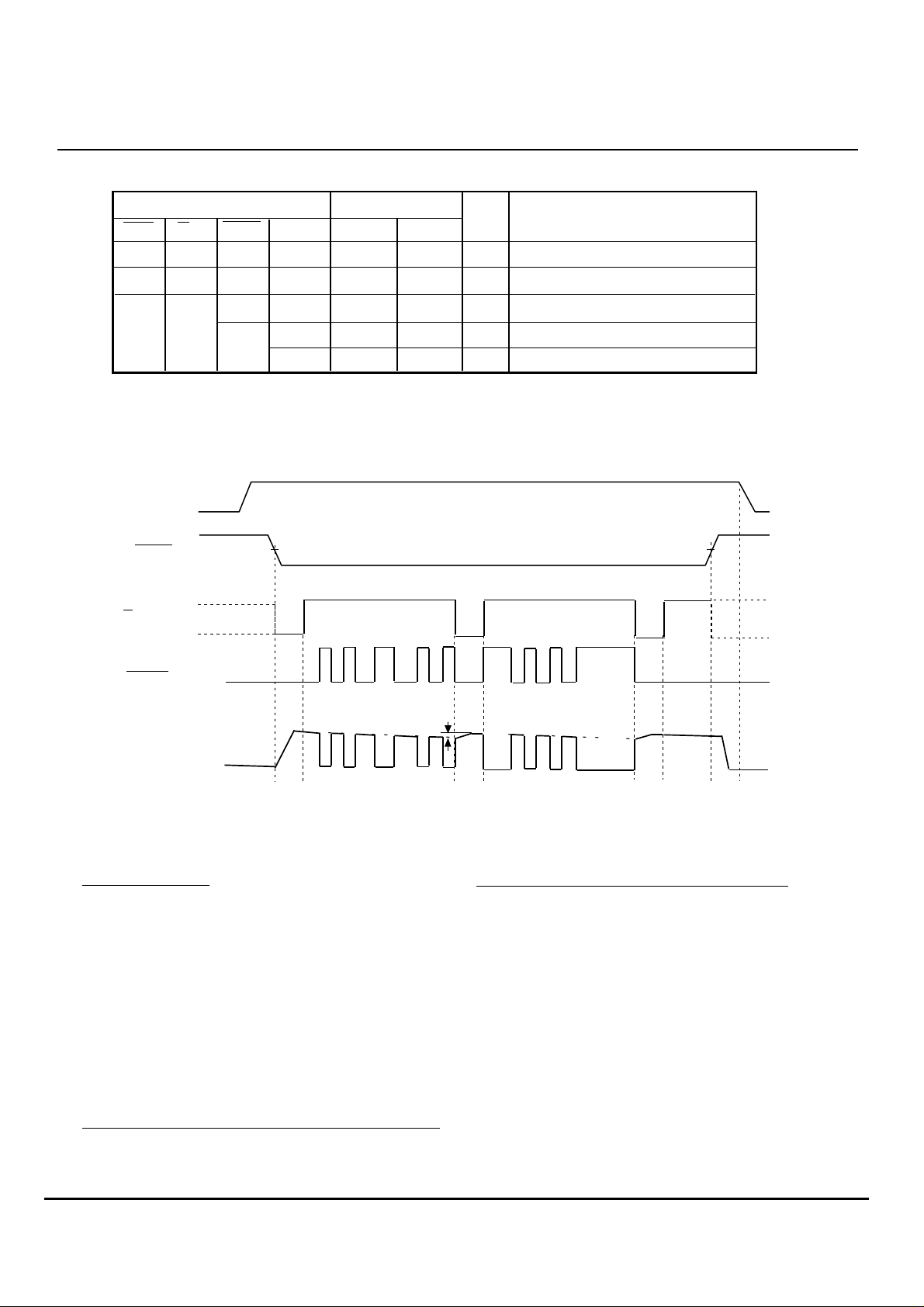
FUNCTION TABLE
MITSUBISHI < DIGITAL ASSP >
M61880FP
Laser-diode driver / controller
Input
ENB S/H Vm,Vr
H
L
X : Don't care
(2) APC Timing Chart
The following diagram is an APC timing chart, operation
of which is based on sample hold control signals.
DATA
X
HL
L
X
X
H
L
X
X
X
Vm < Vr
Vm > Vr
Switch condition
SW1 SW2
OFF
OFF OFF
OFF
ON
OFF
OFF
OFF
OFF
ON
Vcc
ENB input
sample
S / H input
hold
Tr1
ON
OFF
OFF
OFF
OFF
sample
Output
Fixed to "L"
High impedance state (hold)
High impedance state (hold)
Constant current sourcing (sample)
Constant current sinking (sample)
Note that in the example it is assumed that the leak current
occurring at the CH pin under hold condition flows into
the M61880 (in the positive direction).
sample
hold
hold
DATA input
∆I LD
Laser drive current
An example of APC Timing Chart
7.Vcc and GND Pins
Pins related to the power supply function are Vcc1, Vcc2,
GND1, and GND2. The role of these pins in terms of the internal circuits are as follows.
Vcc1, GND1: connected to analog circuits
Vcc2, GND2: connected to digital circuits
In practical wiring, the following should be noted.
(1) Secure as much a width as possible for conductors and
avoid lengthy wiring.
(2) Allocate electrolytic capacitors for stable voltage near
Vcc1 and GND1.
(3) Allocate by-pass capacitors near Vcc2 and GND2.
Notes on the Wiring for Peripheral Components
Lay out peripheral components necessary for the M61880 to
operate in closest possible proximity to the M61880.
Calculation Method for Power Dissipation
The approximate power dissipation, P, of the M61880FP is
determined by the following equation.
P = Icc x Vcc + I(RO) x V(RO) + I(LD) x V(LD) where
V(RO):voltage at RO pin
V(LD): voltage at LD pin
I(RO): load current at RO pin
I(LD) : load current at LD pin
If, for example, Vcc = 5.25V, V(RO) = V(LD) = 2.5V, and I(RO)
= I(LD) = 100mA, power dissipation at times of turning laser
on and off will be as follows.
(1) Laser ON (DATA = "L" and Icc = 55mA)
PON = 55 x 5.25 + 0 + 100 x 2.5 = 538.8(mW)
(2) Laser OFF (DATA = "H" and Icc = 55mA)
POFF = 55 x 5.25 +0+100 x 2.5 = 538.8(mW)
4
11
( / )

MITSUBISHI < DIGITAL ASSP >
M61880FP
Laser-diode driver / controller
ABSOLUTE MAXIMUM RATINGS (Ta = -20 ~ 70°C unless otherwise noted)
Symbol
Vcc
VI
VO
Isw
IB
Pd
Tstg
Note: For operation above 25°C, derating of 9.8mW/°C is necessary.
Supply voltage
Input voltage
Output voltage
Switching current
Bias current
Power dissipation
Storage temperature
Parameter
CH, Vr
DATA, ENB, S/H
RO
RECOMMENDED OPERATIONAL CONDITIONS (Ta = -20 ~ 70°C unless otherwise noted)
Symbol Parameter
Vcc
Isw
IB
Topr
Note: Isw + IB ≤ 100mA
Supply voltage
Switching current
Bias current
Operating ambient temperature
4.75
ELECTRICAL CHARACTERISTICS (Ta = -20 ~ 70°C, Vcc = 5V±5% unless otherwise noted)
Symbol
VIH
VIL
Vr
Vref
VLD
VI
VOH
VOL
II
Isw
IB
Icg
Idg
Ioz
LOFF
Icc
"H" Input voltage
"L" Input voltage
Reference voltage input
Reference
voltage
output
Operating voltage range
Maximum effective voltage
"H" output voltage
"L" output voltage
Input current
Switching current
Bias current (Note)
Load charging current
Load discharge current
Output current under off
condition
Output current under off
condition
Supply current
Parameter
DATA,ENB,S/H
DATA,ENB,S/H
Vr
Vref
Temperature
coefficient
LD
CH
CH
CH
DATA,ENB
LD
LD
CH
CH
CH
LD
Conditions
Measured being mounted
Ta = 25°C(Note)
Limits
Typ.
Min.
5.0 5.25
Test conditions
Io = ±10µA
Ta = -20 ~ 25°C
Ta = 25 ~ 70°C
ENB= "L" ,IoL= (-0.6mA)
ENB= "L" ,IoH= (0.6mA)
VI = 2.7V
VI = 0.4V
CH=3.5V,Rs=1.2kΩ,VLD=3V
VB=1.5V,RB=70Ω,VLD=3V
ENB= "L" ,Vo=( 0.6 ~ Vcc-1.6V)
ENB= "L" ,Vo=( 0.6 ~ Vcc-1.6V)
Vo=2.0 ~ 3.0V, Hold condition
ENB= "L" ,DATA= "H" ,Isw=50mA
ENB= "H" ,DATA= "L" ,Isw=50mA
Vcc=5.25V,ENB=0V,
CH=3.5V,VB=1.4V
Isw=75mA,IB=25mA
RO=LD=5.0v
Max.
100
40
70-20
Unit
V
mA
mA
°C
DATA=0V
DATA=4.5V
Ratings
-0.3 ~ +5.5
-0.3 ~ +Vcc
-0.3 ~ +Vcc
-0.3 ~ +Vcc
120
50
980
-60 ~ +150
Min. Typ. Max.
2.0
0.35
1.4
2.5
2.7 3.0
Vcc-1.6
-0.2
0.66
-0.5
Unit
V
V
V
mA
mA
mW
°C
Limits
1.5
0.1
-0.1
75
20
-1.0
43 63
43
1.0
0.8
2.0
1.6
Vcc
0.6
20
-0.66
+0.5
50
50
63
Unit
V
V
V
V
mV/°C
V
V
V
V
µA
mA
mA
mA
mA
mA
µA
µA
µA
mA
*Typical values are gained under conditions of Ta=25°C and Vcc=5V.
Note: This parameter indicates the conversion characteristics of the input voltage and output current.In actual use, Isw and IB
shall be within the range specified as limits in the recommended operating conditions.
11
5
( / )

MITSUBISHI < DIGITAL ASSP >
SWITCHING CHARACTERISTICS (Ta=25°C,Vcc=5V)
M61880FP
Laser-diode driver / controller
Symbol
fop
tRP1
tRP2
tON
tOFF
NOTE1:TEST CIRCUIT
oscilloscope
(Input)
P. G.
0.047µF
50Ω
840Ω
RM
Parameter
Operating frequency
Circuit response time1
Circuit response time2
Circuit ON time
Circuit OFF time
20Ω
Vcc
CH
Vr
RS
1RM
2RM
RO
P D
L D
S / H
DATA
ENB
GND
Other pins are open
ENB voltage
ENB voltage
ILD
Current probe
Test pin
Input
Vr voltage
Vr voltage
L DP D
oscilloscope
( Output )
Output
LD current
LD current
LD current
LD current
NOTE2:TEST CIRCUIT
0.047µF
Test condition
ILD=50mA, Rs=840Ω,
CH=0.047µF
APC adjustment;
RM=adjustment(CH=2.5V)
Vr=1.5V± 0.5% (Note1)
ILD=50mA, Rs=840Ω,
CH=0.047µF
APC adjustment;
RM=adjustment(CH=2.5V)
Vr=1.5V± 2.5% (Note1)
ILD(H)=50mA (Note2)
ILD(H)=50mA (Note2)
20Ω
Vcc
1.5V
840Ω
RM
CH
Vr
RS
1RM
2RM
GND
RO
P D
L D
S / H
DATA
ENB
Other pins are open
Min.
Limits
Typ.
100
1
3
ILD
50Ω
Unit
Max.
Mbps
µS
µS
350
µS
5
µS
LDPD
oscilloscope
( Output )
Current probe
oscilloscope
( Input )
P.G.
t r=t f= 6ns
TIMING CHARTS
1.5V
Vr voltage
LD current
0%
TRP1(TRP2)
10%
TRP1(TRP2)
90%
1.5V± change value
ILD(H)
ILD(L)
6
( / )
TIMING CHARTS
ENB
voltage
LD
current
11
1.5V
TON
90 %
1.5 V
TOFF
10 %
3 V
0 V
ILD (H)
ILD (L)

APPLICATION EXAMPLE
LD driver M61880FP
1920
RO
10Ω
300pF
36Ω
N C
18
5V
Vcc2
digital
5V
MITSUBISHI < DIGITAL ASSP >
M61880FP
Laser-diode driver / controller
Vcc
Control signal
Data stream
LD
+
GND2
digital
PD
TTL/ECL
DATA
14151617
2RM 1RM
ENB
111213
1
RS
1.5KΩ
IB
2 3
GND1
analog
RB
150Ω
VB
ISW
50K
4
Vref Vr
2.5V
Reference
voltage
1.5V
5 6
0.047µF
7
8
S/H
S/H signal
COMP
9 10
Vcc1
analog
5V
NC
7
11
( / )

MITSUBISHI < DIGITAL ASSP >
The circuit of setting center
value (Isw0)of maximum
switching current(2X Isw0)
Explanation for setting Laser switching current
Vcc
1:1
D1
1.5V
Vcc
2XISWO
+
AMP1
–
RS
2XISWO
ISW2
ISW
2.5V
I1
V1
M61880FP
Laser-diode driver / controller
ISW1
ISW2
Q1 Q2
∆Vd
2KΩ
D2
I2
V2
Id
VB
CH
LD
CURRENT SW
1:1
Fig.1 Equivalent circuits of setting switching current
1. The circuit of setting center value(Isw0) of
maximum switching current
The setting center value(Isw0) of maximum switching
current, 2 X Isw0,set up Rs ( load for switching current
setting). Isw0 (the value that is initialized) is
Isw0[mA]=30 x
2. The circuit of setting switching current
When ∆V is a difference voltage of between
CHpin and 2.5V,Id is
Id =
So I1 and I2 is as follows
I1=250µA-Id
(
I2=250µA+Id
Vref(1.5V)[V]
∆V
2KΩ
RS[kΩ]
(1)
(2)
(3)
250µA
2XISWO
250µA
The circuit of setting switching current
So Isw2 is
Isw2=2 • Isw0 x
Isw is as follows
Isw=2 • Isw0-Isw2 (7)
Next the relation between Isw and ∆V would be introduced .
Isw is able to solve with (6), (7),(3) and (2)equation.
Isw=2 • Isw0( )
Isw=Isw0(1+ )
Isw=Isw0(1+ )
I1+I2
I2
I1+I2
Id
250µA
∆V/2KΩ
250µA
I1
(6)
(8)
(9)
(10)
D1,D2,Q1 and Q2 construct a Gilbert circuit.
The relation of I1,I2,Isw1, Isw2 and Isw0 is
I1I2Isw2
=
Isw1
Isw1+Isw2=2 • Isw0
(4)
(5)
11
8
( / )

TYPICAL CHARACTERISTICS
MITSUBISHI < DIGITAL ASSP >
M61880FP
Laser-diode driver / controller
THERMAL DERATING
1200
1000
800
600
400
200
0
AMBIENT TEMPERATURE Ta (°C)
25 75 125
VB PIN INPUT VOLTAGE •
BIAS OUTPUT CURRENT
60
50
40
30
20
10
0
Vcc=5V,Ta=25°C
RB=51Ω
1.5 2.5 3.5
INPUT VOLTAGE VB (V)
Reference Voltage -Ambient Temperature
Vcc=5V
1.54
1.52
1.50
1.48
1.46
1.44
100500-25
0
AMBIENT TEMPERATURE Ta (°C)
25 75 125
100500-25
VB PIN INPUT VOLTAGE-CURRENT
100.0
90.0
80.0
70.0
60.0
50.0
40.0
30.0
20.0
10.0
3.02.01.00.5
0
0
INPUT VOLTAGE VB (V)
Vcc=5V,Ta=25°C
1.0
2.0
BIAS CURRENT SET RESISTOR BIAS OUTPUT CURRENT
60
50
40
30
20
10
0
0 100
RESISTOR FOR BIAS CURRENT SET RB(Ω)
Vcc=5V,Ta=25°C
VB=1.5V
200
300 400
( 9 /11)
SWITCHING CURRENT SET RESISTOR SWITCHING OUTPUT CURRENT
120
100
80
60
40
20
0
0 1
RESISTOR FOR SWITCHING CURRENT SET Rs(KΩ)
Vcc=5V,Ta=25°C
VCH=2.5V
2
3 4
CHpin VOLTAGE - SWITCHING CURRENT
120
100
Vcc=5V,Ta=25°C
80
60
40
20
0
1 1.5 2 2.5 3 3.5
Rs=820Ω
CHpin VOLTAGE Vch(V)
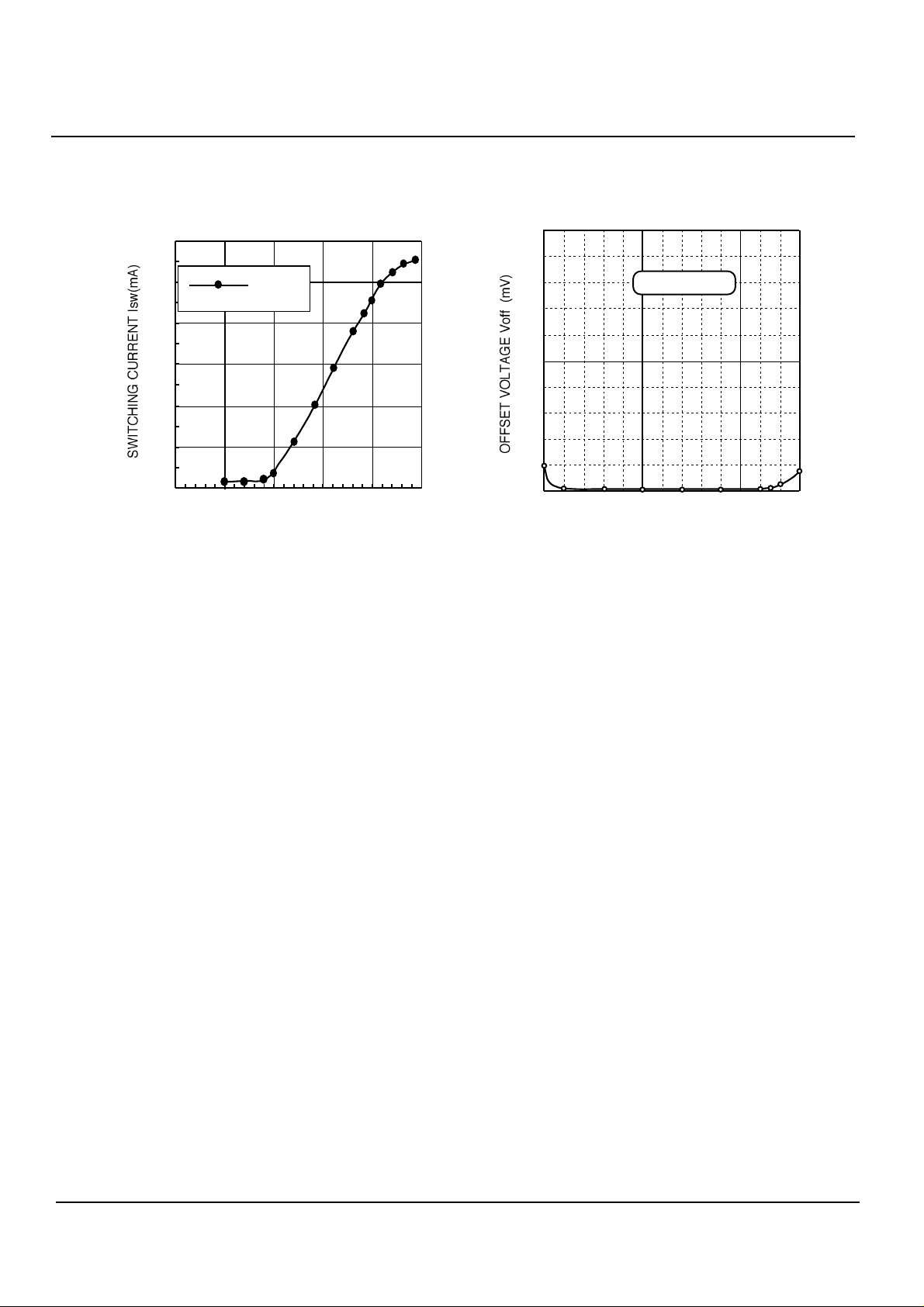
MITSUBISHI < DIGITAL ASSP >
M61880FP
Laser-diode driver / controller
APC COMPARATOR
INPUT VOLTAGE-OFFSET VOLTAGE
10.0
9.0
8.0
7.0
6.0
5.0
4.0
3.
0
2.0
1.0
0
0
2RMpin INPUT VOLTAGE Vm (V)
Vcc=5V,Ta=25°C
1.0
2.0
( 10/11)

PACKAGE OUTLINE
MITSUBISHI < DIGITAL ASSP >
M61880FP
Laser-diode driver / controller
11
11
( / )
 Loading...