PRELIMINARY
BUILT-IN 2-CHANNEL SPD SENSOR DETECT AMOUNT OF LIGHT
DESCRIPTION
The M61016F is a semiconductor integrated circuit designed to
detect quantity of light and used for cameras and illuminometers.
Because a high-sensitivity SPD sensor is built in this IC, it is
possible not only to reduce the space and expenses to mount it but
also to conduct wide-ranging detection of light volume.
MITSUBISHI ICS<AV COMMON>
M61016F
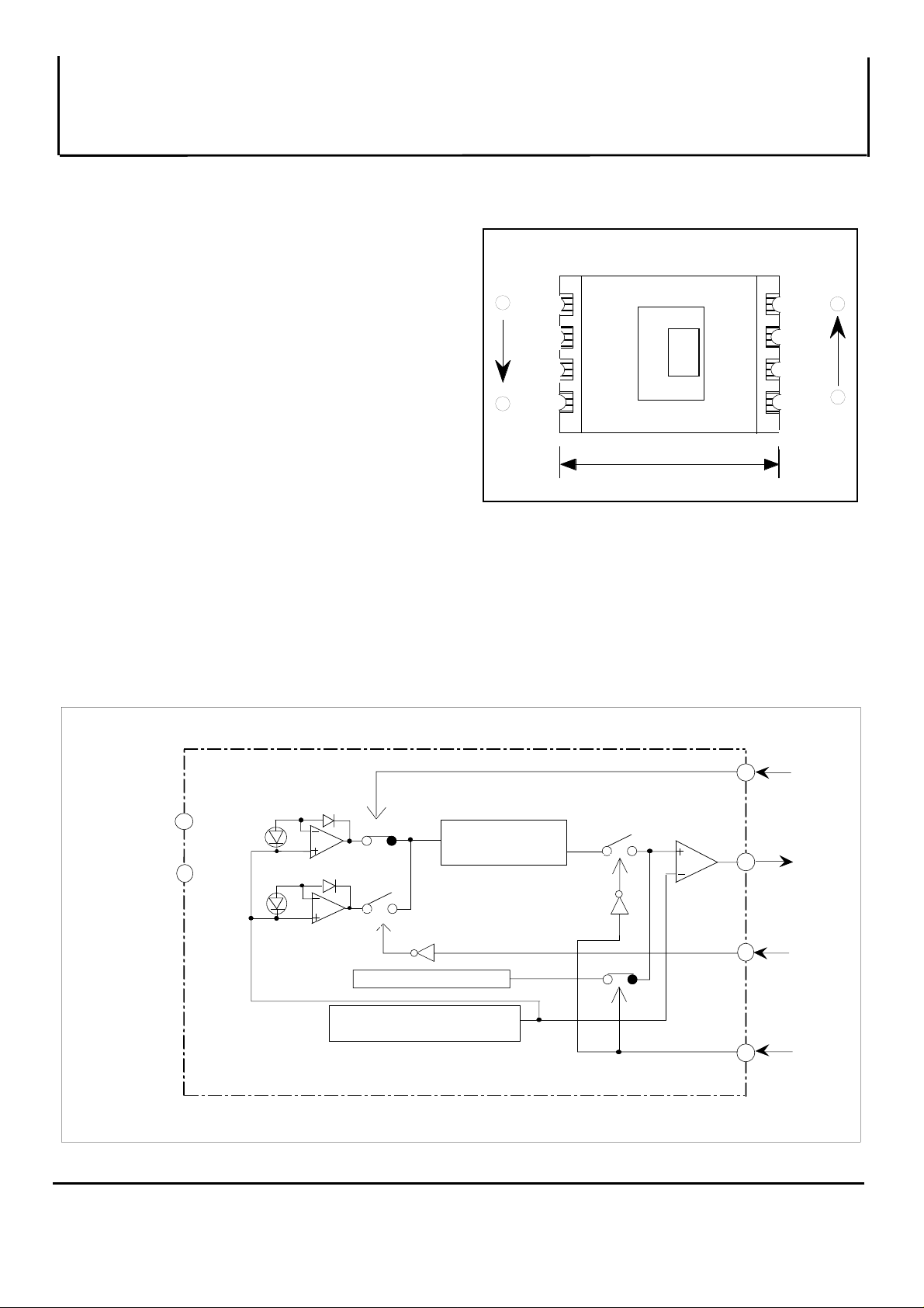
PIN CONFIGURATION (TOP VIEW)
FEATURES
• A 2-channel SPD sensor is built in.(1-channel for spot and one
for average)
• Wide-ranging detection of light volume.
• One output pin (thermometer output and photometry output)
• Small-sized transparent molded plastic package.
APPLICATION
Automatic exposure control for cameras,illuminometers.
RECOMMENDED OPERATING CONDITION
Supply voltage range • • • • • • • • • • • • • • • • • • 4.0 to 6.5V
Rated supply voltage • • • • • • • • • • • • • • • • • • • • • • 5V
Light input range • • • • • • • • • • • SPOT 2 to 100000 lux
*
* Decide after confirmation of real power
BLOCK DIAGRAM
AVE 0.125 to 12500 lux
1
4
GND
CS1
CS2
SEL
5mm
VCC
N.C.
N.C.
VOUT
8
5
VCC
GND
SPOT
SPD
AVE
SPD
TEMPERATURE
SW1
SW2
THERMOMETER CIRCUIT
1.1 V
(T-PROPORTIONAL VOLTAGE)
COMPENSATION
500nA CONSTANT CURRENT
MITSUBISHI
1
( / 8 )
SW3
SW4
CS1
VOUT
GAIN
x 7
CS2
SEL

MITSUBISHI ICS<AV COMMON>
y
g
y
PRELIMINARY
BUILT-IN 2-CHANNEL SPD SENSOR DETECT AMOUNT OF LIGHT
ABSOLUTE MAXIMUM RATINGS (Ta=25°C, unless otherwise noted)
S
mbol Parameter Conditions Ratings
VCC Supply voltage
Pd Power dissipation
VIN Input voltage
IO(max)
Topr
Tstg
K
Output current
Operating temperature
e temperature
Stora
Thermal derating
RECOMMENDED OPERATING CONDITION (Ta=25°C, unless otherwise noted)
S
mbol Parameter
Supply voltage
Operating illuminance " SP "
*
*
VCC
Lopr1
Lopr2
Operating illuminance " AVE "
* Decide after confirmation of real power
Pin VOUT
Test Conditions
2 to 100000
0.125 to 12500
M61016F
-0.3 to 7.0
150
-0.3 to VCC+0.3
0.2
-10 to 50
-30 to 85
-2.5
Limits
Min Typ Max
4.0
5.0 6.5 V
Unit
V
mW
V
mA
°C
°C
mW/°C
Unit
lux
lux
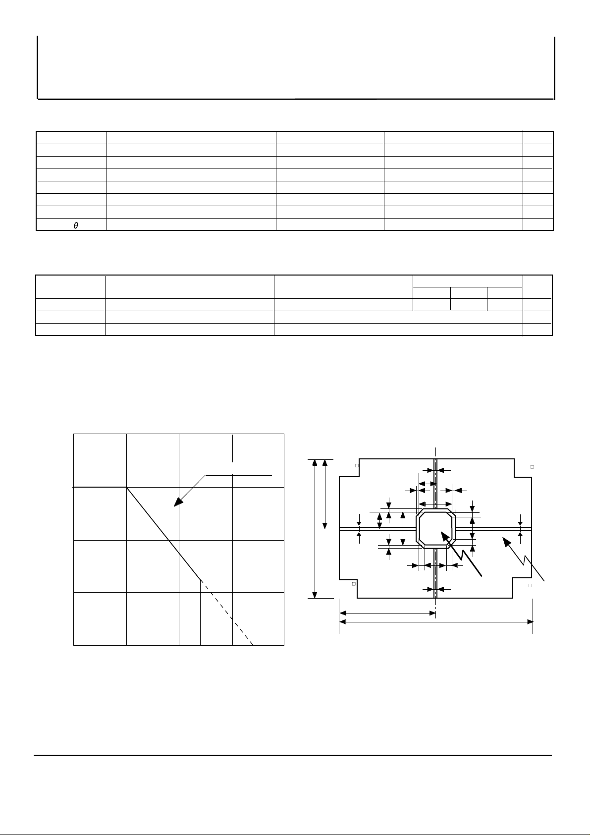
THERMAL DERATING (MAXIMUM RATING)
200
180
150
100
POWER DISSIPATION Pd (mW)
50
25 50
AMBIENT TEMPERATURE Ta (°C)
- 2.5 mW/°C
75
85
SENSOR FORM
Unit : µm
200
50
450
900
200
10060
6
50
140
280
50
750
Area ratio
78 78
SPOT : AVE = 1 : 16
140
280
1500
6
50
78
78
6
SPOT
200
6
200
AVE
MITSUBISHI
2
( / 8 )

MITSUBISHI ICS<AV COMMON>
x
PRELIMINARY
M61016F
BUILT-IN 2-CHANNEL SPD SENSOR DETECT AMOUNT OF LIGHT
ELECTRICAL CHARACTERISTICS (Ta=25°C, light source 4500°K, illuminance: measured after transmitting products through CM 500 filter, unless otherwise noted)
Block
I / F
Thermo
-meter
SPOT
Symbol
ICC illuminance: 200 lux 6 mA4
VTHCS1 VCC-0.8VCC-2.2 VCS1 input pin
CS1I Ground current 1 -150 -16 µA
VTHCS2 VCC-0.8VCC-2.2CS2 input pin
CS2I Ground current 2
VHSEL VCC-0.8VCC-2.2SEL input pin
SELI
Absolute value of thermometer output
VTE
Thermometer supply voltage variance 1
dVTE1
Thermometer supply voltage variance 2
dVTE2
dVTE3
dVOS1 -45 45
dVOS2
dEVS1
dEVS2
dEVS3 SP side ,illuminance 2 to 4 lux 0.5
Thermometer output voltage load variance
Variance of thermometer output dVTE4 mV/ºC
Absolute value of photometry output
VOS SP side , illuminance 8 lux 2120 2440 2760
Photometry output supply voltage variance 1
Photometry output supply voltage variance 2
Photometry output linearity 1
Photometry output linearity 2
Parameter Test Conditions
Circuit current
Current of between CS1pin to GND VCC = 5V
Threshold voltage 2
Current of between CS2pin to GND VCC = 5V
Threshold voltage 3
Ground current 3
Variance per level (1EV)
Current of between SELpin to GND VCC = 5V
Output voltage variance at VCC=5V+1V
Output voltage variance at VCC=5V-1V
Load current : - 0.2mA 20-20
SP side ,Output voltage variance at VCC=5V+1V
SP side ,Output voltage variance at VCC=5V-1V
SP side ,Variance when illuminance changes from 8 to 32
SP side ,illuminance 4 to * lux
-24.3
Limits
Min Typ
Max
-
VCC-1.5Threshold voltage 1
-50
VCC-1.5
VCC-1.5
-150 -16-50
960
-45 45
-45 45
1200
-
-
-
-22.1
-
-45 45
-
-116-125-134
-
-0.5
-
1440
-19.9
0.3-0.3
Unit
V
µA-150 -16-50
V
µA
mV
mV
EV
AVE
Response
Absolute value of photometry output
VOA AVE side ,illuminance 8 lux 1680 1940 2200
dVOA1 -45 45
dVOA2
dEVA1
dEVA2 AVE side ,illuminance 0.25 to * lux 0.3-0.3
dEVA3 AVE side ,illuminance 0.125 to 0.25 lux 0.5
Photometry output supplyvoltage variance 1
Photometry output supplyvoltage variance 2
Variance per level (1EV)
Photometry output linearity 1
Photometry output linearity 2
trs SP side , illuminance 2 lux 20
tra AVE side , illuminance 0.5 lux 50
trc1 Switching response 1 SP AVE , illuminance 0.125 to 12500 lux 3000
trc2 Switching response 2 3000
Power supply response 1
Power supply response 2
AVE side ,Output voltage variance at VCC=5V+1V
AVE side ,Output voltage variance at VCC=5V-1V
AVE side ,Variance when illuminance changes from 8 to 32
AVE SP , illuminance 2 to 100000 lu
-
-45 45
-
-116-125-134
-
-0.5
-
-
-
-
-
5
20
10
10
* Decide after confirmation of real power
MITSUBISHI
3
( / 8 )
mV
EV
ms
µS
 Loading...