Mitsubishi M5M5Y5672TG-20, M5M5Y5672TG-22 Datasheet
MITSUBISHI
ELECTRIC
Advanced Information
M5M5Y5672TG REV.0.1
2001.May Rev.0.1
Advanced Information
Notice: This is not final specification.
Some parametric limits are subject to change.
DESCRIPTION
The M5M5Y5672TG is a family of 18M bit synchronous SRAMs
organized as 262144-words by 72-bit. It is designed to eliminate
dead bus cycles when turning the bus around between reads
and writes, or writes and reads. Mitsubishi's SRAMs are
fabricated with high performance, low power CMOS technology,
providing greater reliability. M5M5Y5672TG operates on a single
1.8V power supply and are 1.8V CMOS compatible.
FEATURES
• Fully registered inputs and outputs for pipelined operation
• Fast clock speed: 250, 225, and 200 MHz
• Fast access time: 2.6, 2.8, 3.2 ns
• Single 1.8V +150/-100mV power supply VDD
• Separate VDDQ for 1.8V I/O
• Individual byte write (BWa# - BWh#) controls may be tied
LOW
• Single Read/Write control pin (W#)
• Echo Clock outputs track data output drivers
• ZQ mode pin for user-selectable output drive strength
• 2 User programmable chip enable inputs for easy depth
expansion
• Linear or Interleaved Burst Modes
• JTAG boundary scan support
APPLICATION
High-end networking products that require high bandwidth, such
as switches and routers.
FUNCTION
PACKAGE
Bump Body Size Bump Pitch
M5M5Y5672TG 209(11X19) bump BGA 14mm X 22mm 1mm
PART NAME TABLE
MITSUBISHI LSIs
M5M5Y5672TG – 25,22,20
18874368-BIT(262144-WORD BY 72-BIT) NETWORK SRAM
Synchronous circuitry allows for precise cycle control triggered
by a positive edge clock transition.
Synchronous signals include : all Addresses, all Data Inputs,
all Chip Enables (E1#, E2, E3), Address Advance/Load (ADV),
Byte Write Enables (BWa#, BWb#, BWc#, BWd#, BWe#, BWf#,
BWg#, BWh#), Echo Clock outputs (CQ1, CQ1#, CQ2, CQ2#)
and Read/Write (W#). Write operations are controlled by the
eight Byte Write Enables (BWa# - BWh#) and Read/Write(W#)
inputs. All writes are conducted with on-chip synchronous
self-timed write circuitry.
The Echo Clocks are delayed copies of the RAM clock, CLK.
Echo Clocks are designed to track changes in output driver
delays due to variance in die temperature and supply voltage.
The ZQ pin supplied with selectable impedance drivers, allows
selection between nominal drive strength (ZQ LOW) for
multi-drop bus application and low drive strength (ZQ floating or
HIGH) point-to-point applications.
The sense of two User-Programmable Chip Enable inputs (E2,
E3), whether they function as active LOW or active HIGH inputs,
is determined by the state of the programming inputs, EP2 and
EP3.
The Linear Burst order (LBO#) is DC operated pin. LBO# pin
will allow the choice of either an interleaved burst, or a linear
burst.
All read, write and deselect cycles are initiated by the ADV
Low input. Subsequent burst address can be internally
generated as controlled by the ADV HIGH input.
1
Part Name Frequency Access Cycle
M5M5Y5672TG -25 250MHz 2.6ns 4.0ns 550mA 20mA
M5M5Y5672TG -22 225MHz 2.8ns 4.4ns 500mA 20mA
M5M5Y5672TG -20 200MHz 3.2ns 5.0ns 450mA 20mA
Active Current
(max.)
Standby Current
(max.)
MITSUBISHI
ELECTRIC
Advanced Information
M5M5Y5672TG REV.0.1
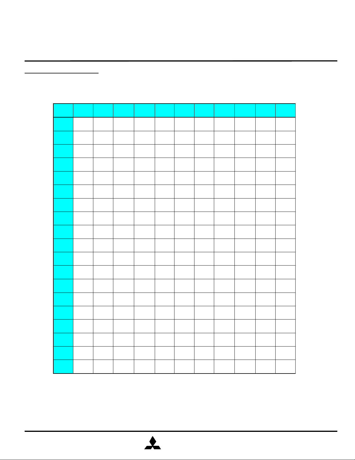
BUMP LAYOUT(TOP VIEW)
209 bump BGA
1 2 3 4 5 6 7 8 9 10 11
A DQg DQg A6 E2 A7 ADV A8 E3 A9 DQb DQb
B DQg DQg BWc# BWg# NC W# A17 BWb# BWf# DQb DQb
C DQg DQg BWh# BWd# NC E1# NC BWe# BWa# DQb DQb
D DQg DQg VSS NC NC MCL NC NC VSS DQb DQb
E DQPg DQPc VDDQ VDDQ VDD VDD VDD VDDQ VDDQ DQPf DQPb
F DQc DQc VSS VSS VSS ZQ VSS VSS VSS DQf DQf
G DQc DQc VDDQ VDDQ VDD EP2 VDD VDDQ VDDQ DQf DQf
MITSUBISHI LSIs
M5M5Y5672TG – 25,22,20
18874368-BIT(262144-WORD BY 72-BIT) NETWORK SRAM
H DQc DQc VSS VSS VSS EP3 VSS VSS VSS DQf DQf
J DQc DQc VDDQ VDDQ VDD MCH VDD VDDQ VDDQ DQf DQf
K CQ2 CQ2# CLK NC VSS MCL VSS NC NC CQ1# CQ1
L DQh DQh VDDQ VDDQ VDD MCH VDD VDDQ VDDQ DQa DQa
M DQh DQh VSS VSS VSS MCL VSS VSS VSS DQa DQa
N DQh DQh VDDQ VDDQ VDD MCH VDD VDDQ VDDQ DQa DQa
P DQh DQh VSS VSS VSS MCL VSS VSS VSS DQa DQa
R DQPd DQPh VDDQ VDDQ VDD VDD VDD VDDQ VDDQ DQPa DQPe
T DQd DQd VSS NC NC LBO# NC NC VSS DQe DQe
U DQd DQd NC A3 NC A15 NC A11 NC DQe DQe
V DQd DQd A5 A4 A16 A1 A13 A12 A10 DQe DQe
W DQd DQd TMS TDI A2 A0 A14 TDO TCK DQe DQe
Note1. MCH means “Must Connect High”. MCH should be connected to HIGH.
Note2. MCL means “Must Connect Low”. MCL should be connected to LOW.
2
M5M5Y5672TG – 25,22,20
MITSUBISHI
ELECTRIC
Advanced Information
M5M5Y5672TG REV.0.1
DQc
LBO#
DQPc
DQd
DQPd
DQe
DQPe
DQf
DQPf
A0
A1
A2~17
CLK
E2
E1#
E3
BWa#
BWb#
BWc#
BWd#
ADV
W#
VDD
VDDQ
VSS
DQa
DQPa
DQb
DQPb
DQg
DQPg
DQh
DQPh
EP2
EP3
CQ1
CQ1#
CQ2
CQ2#
BWe#
BWf#
BWg#
BWh#
ZQ
18874368-BIT(262144-WORD BY 72-BIT) NETWORK SRAM
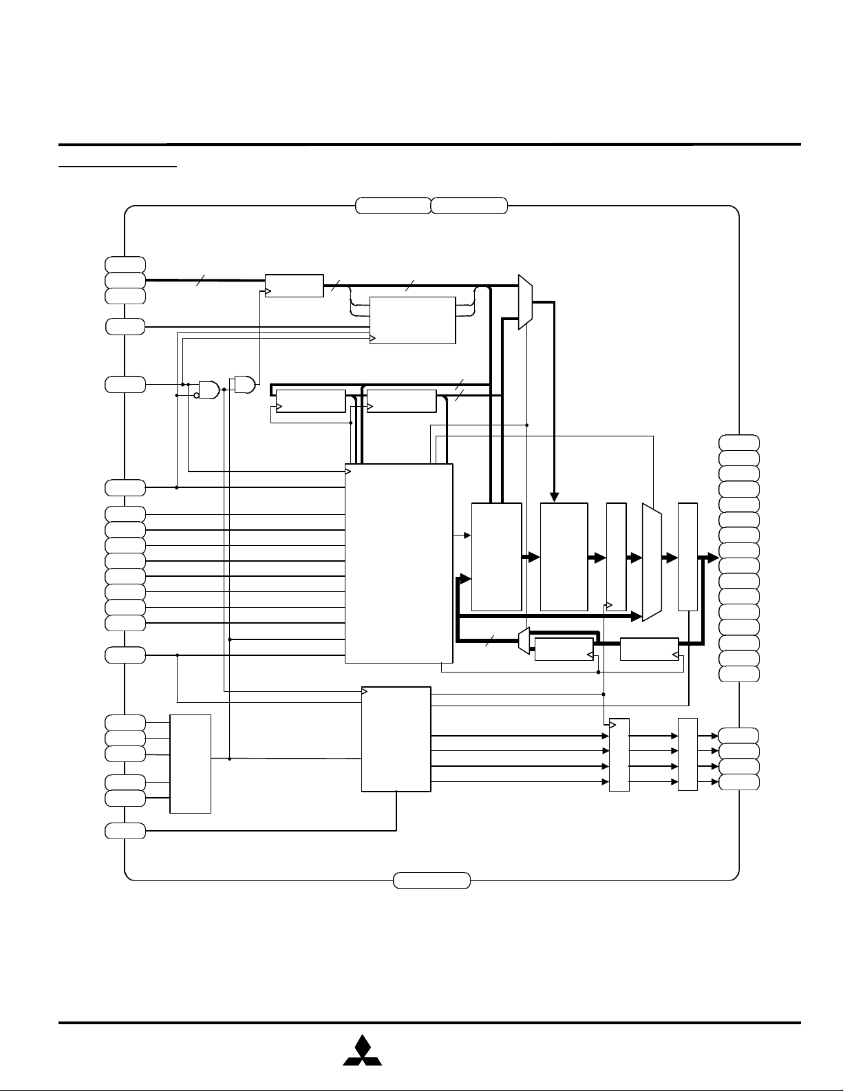
BLOCK DIAGRAM
Note3. The BLOCK DIAGRAM does not include the Boundary Scan logic. See Boundary Scan chapter.
Note4. The BLOCK DIAGRAM illustrates simplified device operation. See TRUTH TABLE, PIN FUNCTION
and timing diagrams for detailed information.
CHIP ENABLE
CONTROL
LOGIC
18
ADDRESS
REGISTER
WRITE ADDRESS
REGISTER1
18 16
A1
D1
LINEAR/
A0
INTERLEAVED
D0
BURST
COUNTER
WRITE ADDRESS
REGISTER2
WRITE REGISTRY
AND
DATA COHERENCY
CONTROL LOGIC
READ
LOGIC
A1'
Q1
A0'
Q0
18
18
BYTE a
|
BYTE h
WRITE
DRIVERS
72
128Kx72
MEMORY
ARRAY
INPUT
REGISTER1
ECHO CLOCK
OUTPUT REGISTERS
OUTPUT REGISTERS
INPUT
REGISTER0
MITSUBISHI LSIs
OUTPUT BUFFERS
OUTPUT SELECT
ECHO CLOCK
OUTPUT BUFFERS
3

MITSUBISHI
ELECTRIC
Advanced Information
M5M5Y5672TG REV.0.1
PIN FUNCTION
Pin Name Function
A0~A17
BWa#, BWb#,
BWc#, BWd#,
Bwe#, BWf#,
BWg#, BWh#
CLK Clock Input
E1#
E2, E3
EP2, EP3
ADV
CQ1, CQ1#,
CQ2, CQ2#
ZQ
W#
DQa,DQPa,DQb,DQPb,
DQc,DQPc,DQd,DQPd,
DQe,DQPe,DQf,DQPf,
DQg,DQPg,DQh,DQPh
LBO#
VDD VDD Core Power Supply
VSS VSS Ground
VDDQ VDDQ I/O buffer Power supply
TDI Test Data Input
TDO Test Data Output
TCK Test Clock
TMS Test Mode Select
MCH Must Connect High These pins should be connected to HIGH
MCL Must Connect Low These pins should be connected to LOW
NC No Connect These pins are not internally connected and may be connected to ground.
Synchronous
Address
Inputs
Synchronous
Byte Write
Enables
Synchronous
Chip Enable
Synchronous
Chip Enable
Chip Enable
Program Pin
Synchronous
Address
Advance/Load
Echo Clock
Outputs
Output
Impedance
Control
Synchronous
Read/Write
Synchronous
Data I/O
Burst Mode
Control
MITSUBISHI LSIs
M5M5Y5672TG – 25,22,20
18874368-BIT(262144-WORD BY 72-BIT) NETWORK SRAM
These inputs are registered and must meet the setup and hold times around the rising edge of
CLK. A0 and A1 are the two least significant bits (LSB) of the address field and set the internal
burst counter if burst is desired.
These active LOW inputs allow individual bytes to be written when a WRITE cycle is active and
must meet the setup and hold times around the rising edge of CLK. BYTE WRITEs need to be
asserted on the same cycle as the address. BWs are associated with addresses and apply to
subsequent data. BWa# controls DQa, DQPa pins; BWb# controls DQb, DQPb pins; BWc#
controls DQc, DQPc pins; BWd# controls DQd, DQPd pins; BWe# controls DQe, DQPe pins;
BWf# controls DQf, DQPf pins; BWg# controls DQg, DQPg pins; BWh# controls DQh, DQPh pins.
This signal registers the address, data, chip enables, byte write enables and burst control inputs
on its rising edge.
All synchronous inputs must meet setup and hold times around the clock's rising edge.
This active LOW input is used to enable the device and is sampled only when a new external
address is loaded (ADV is LOW).
These pins are user-programmable chip enable inputs. The sense of the inputs, whether they
function as active LOW or HIGH inputs, is determined by the state of the programming inputs,
EP2 and EP3.
These pins determine the sense of the user-programmable chip enable inputs, whether they
function as active LOW or active HIGH inputs.
When HIGH, this input is used to advance the internal burst counter, controlling burst access after
the external address is loaded. When HIGH, W# is ignored. A LOW on this pin permits a new
address to be loaded at CLK rising edge.
The Echo Clocks are delayed copies of the main RAM clock, CLK.
This pin allows selection between RAM nominal drive strength (ZQ low) for multi-drop bus
applications and low drive strength (ZQ floating or high) point-to-point application.
This active input determines the cycle type when ADV is LOW. This is the only means for
determining READs and WRITEs. READ cycles may not be converted into WRITEs (and vice
versa) other than by loading a new address. A LOW on the pin permits BYTE WRITE operations
and must meet the setup and hold times around the rising edge of CLK. Full bus width WRITEs
occur if all byte write enables are LOW.
Byte “a” is DQa , DQPa pins; Byte “b” is DQb, DQPb pins; Byte “c” is DQc, DQPc pins; Byte “d” is
DQd,DQPd pins; Byte “e” is DQe, DQPe pins; Byte “f” is DQf, DQPf pins; Byte “g” is DQg, DQPg
pins; Byte “h” is DQh, DQPh pins. Input data must meet setup and hold times around CLK rising
edge.
This DC operated pin allows the choice of either an interleaved burst or a linear burst. If this pin is
HIGH or NC, an interleaved burst occurs. When this pin is LOW, a linear burst occurs, and input
leak current to this pin.
These pins are used for Boundary Scan Test.
4
MITSUBISHI LSIs
MITSUBISHI
ELECTRIC
Advanced Information
M5M5Y5672TG REV.0.1
CLK
A B C D E
ADD
E1#
ADV
W#
BWx#
DQ
CQ
Q(A)
Q(B)
Q(C)
Read A
Deselect
Read B
Read C
Read D
Read E
M5M5Y5672TG – 25,22,20
18874368-BIT(262144-WORD BY 72-BIT) NETWORK SRAM
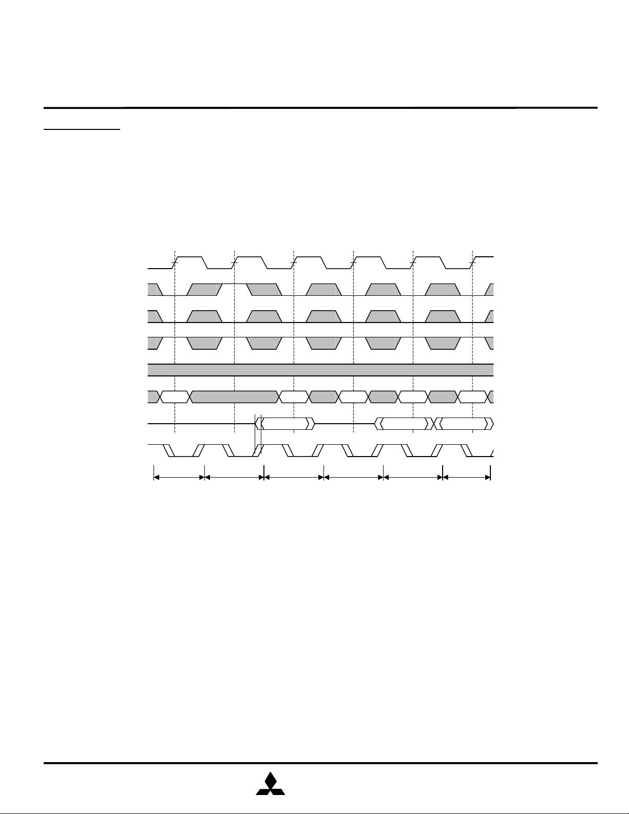
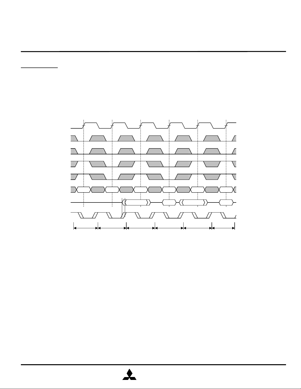
Read Operation
Pipelined Read
Read operation is initiated when the following conditions are satisfied at the rising edge of clock: All three chip enables (E1#, E2 and
E3) are active, the write enable input signal (W#) is deasserted high, and ADV is asserted low. The address presented to the address
inputs is latched into the address register and presented to the memory core and control logic. The control logic determines that a read
access is in progress and allows the requested data to propagate to the input of the output register. At the next rising edge of clock the
read data is allowed to propagate through the output register and onto the output pins.
5
MITSUBISHI LSIs
MITSUBISHI
ELECTRIC
Advanced Information
M5M5Y5672TG REV.0.1
CLK
A C D E F
ADD
E1#
ADV
W#
BWx#
DQ
CQ
Q(A)
Q(C) B D(B)
D(D)
Read A
Write B
Read C
Write D
Read E
Read F
M5M5Y5672TG – 25,22,20
18874368-BIT(262144-WORD BY 72-BIT) NETWORK SRAM
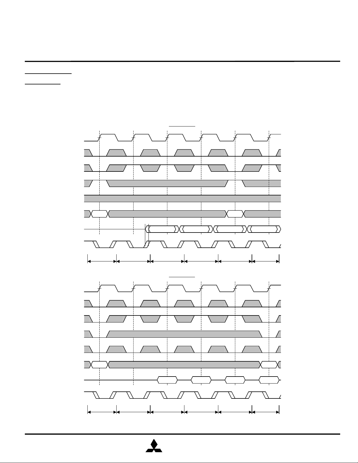
Write Operation
Double Late Write
Write operation occurs when the following conditions are satisfied at the rising edge of clock: All three chip enables (E1#, E2 and E3)
are active and the write enable input signal (W#) is asserted low.
Double Late Write means that Data In is required on the third rising edge of clock. It is designed to eliminate dead bus cycles when
turning the bus around between reads and writes, or writes and reads.
6
MITSUBISHI LSIs
MITSUBISHI
ELECTRIC
Advanced Information
M5M5Y5672TG REV.0.1
CLK
ADD
E1#
ADV
W#
BWx#
DQ
CQ
D(A+3)
Write A
Burst Write
A
D(A+2)
D(A+1)
D(A)
Burst Write
Burst Write
Burst Write
B
Write B
CLK
A
ADD
E1#
ADV
W#
BWx#
DQ
CQ
Q(A)
Q(A+1)
Q(A+2)
Q(A+3)
Read A
Burst Read
Burst Read
Burst Read
Read B
B
Burst Read
Burst Read
Burst Write
M5M5Y5672TG – 25,22,20
18874368-BIT(262144-WORD BY 72-BIT) NETWORK SRAM
Special Function
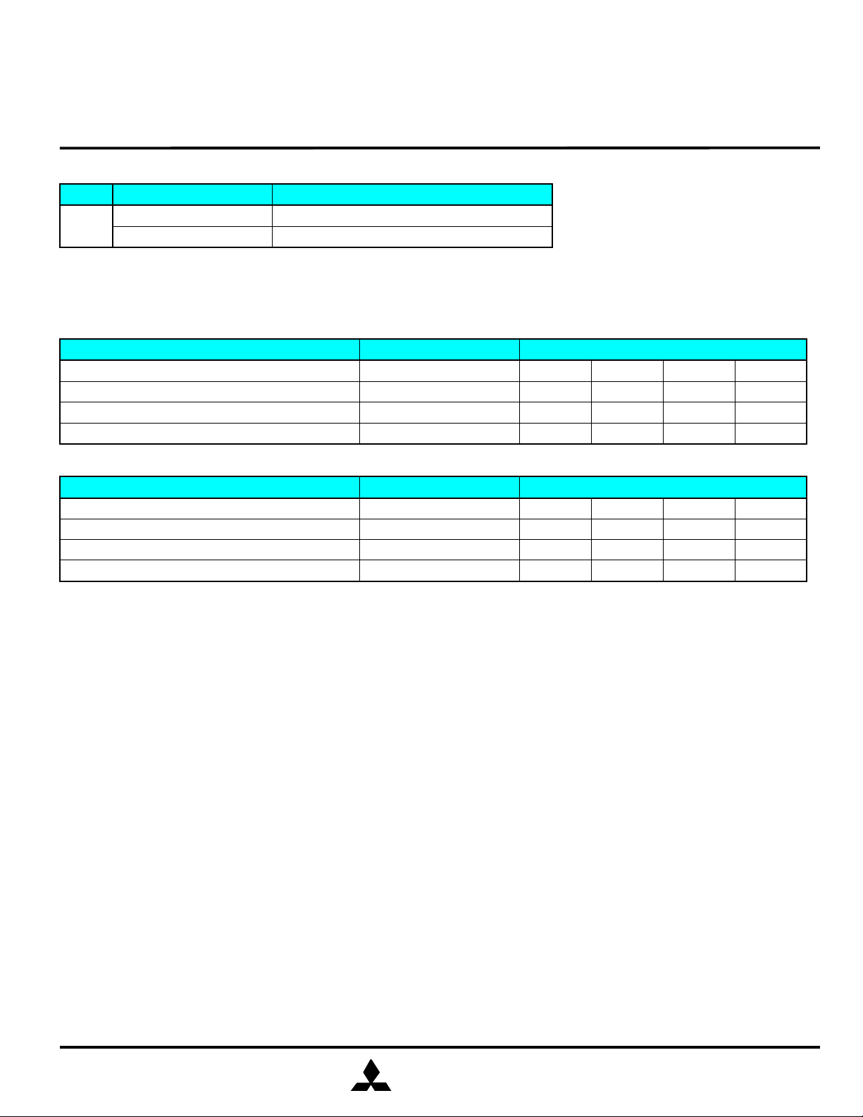
Burst Cycles
The SRAM provides an on-chip burst address generator that can be utilized, if desired, to further simplify burst read or write
implementations. The ADV control pin, when driven high, commands the SRAM to advance the internal address counter and use the
counter generated address to read or write the SRAM. The starting address for the first cycle in a burst cycle series is loaded into the
SRAM by driving the ADV pin low, into Load mode.
A+1
A+1
A+2
A+2
A+3
A+3
B+1
A
7
M5M5Y5672TG – 25,22,20
MITSUBISHI
ELECTRIC
Advanced Information
M5M5Y5672TG REV.0.1
18874368-BIT(262144-WORD BY 72-BIT) NETWORK SRAM
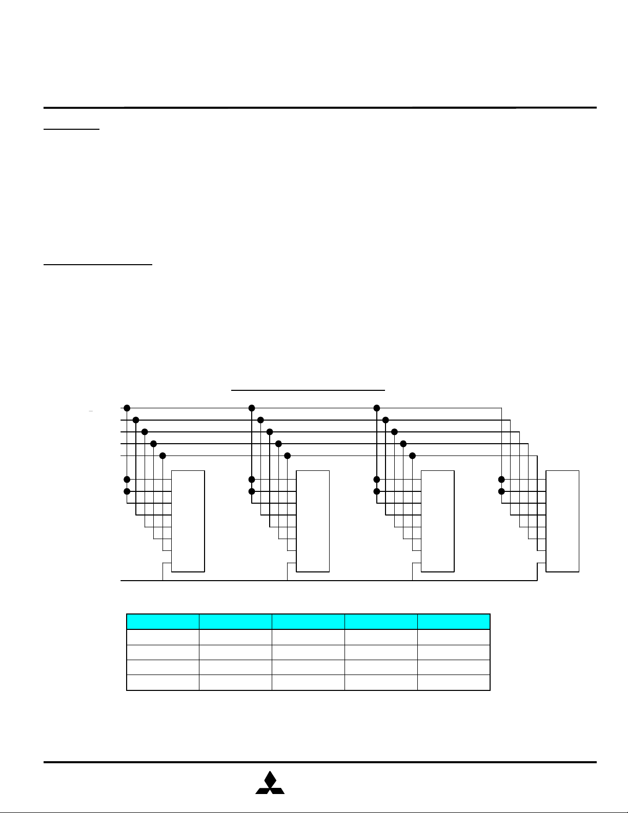
DC OPERATED TRUTH TABLE
Name Input Status Operation
LBO#
Note5. LBO# is DC operated pin.
Note6. NC means No Connection.
Note7. See BURST SEQUENCE TABLE about interleaved and Linear Burst Sequence.
BURST SEQUENCE TABLE
(1) Interleaved Burst Sequence (when LBO# = HIGH or NC)
First access, latch external address A17~A2 0 , 0
Second access(first burst address) latched A17~A2 0 , 1
Third access(second burst address) latched A17~A2 1 , 0
Fourth access(third burst address) latched A17~A2 1 , 1
(2) Linear Burst Sequence (when LBO# = LOW)
First access, latch external address A17~A2 0 , 0
Second access(first burst address) latched A17~A2 0 , 1
Third access(second burst address) latched A17~A2 1 , 0
Fourth access(third burst address) latched A17~A2 1 , 1
Note8. The burst sequence wraps around to its initial state upon completion.
HIGH or NC Interleaved Burst Sequence
LOW Linear Burst Sequence
Operation A17~A2 A1,A0
Operation A17~A2 A1,A0
MITSUBISHI LSIs
0 , 1 1 , 0
0 , 0 1 , 1
1 , 1 0 , 0
1 , 0 0 , 1
0 , 1 1 , 0
1 , 0 1 , 1
1 , 1 0 , 0
0 , 0 0 , 1
1 , 1
1 , 0
0 , 1
0 , 0
1 , 1
0 , 0
0 , 1
1 , 0
8
MITSUBISHI LSIs
MITSUBISHI
ELECTRIC
Advanced Information
M5M5Y5672TG REV.0.1
A
E3#
E2#
E1#
CK
W#
DQ
CQ
Bank0
A0~A19
E1#
CK
W#
DQa~DQh
A0~A17
A18
A19 A E3
E2#
E1#
CK
W#
DQ
CQ
Bank1
A0~A17
A18
A19 A E3#
E2
E1#
CK
W#
DQ
CQ
Bank2
A0~A17
A18
A19 A E3
E2
E1#
CK
W#
DQ
CQ
Bank3
A0~A17
A18
A19
CQ
Example Four Bank Depth Schematic
M5M5Y5672TG – 25,22,20
18874368-BIT(262144-WORD BY 72-BIT) NETWORK SRAM
Echo Clock
The SRAM features Echo Clocks, CQ1,CQ2, CQ1#, and CQ2# that track the performance of the output drivers. The Echo Clocks are
delayed copies of the main RAM clock, CLK. Echo Clocks are designed to track changes in output driver delays due to variance in
die temperature and supply voltage. The Echo Clocks are designed to fire with the rest of the data output drivers. The SRAM
provide both in-phase, or true, Echo Clock outputs (CQ1 and CQ2) and inverted Echo Clock outputs (CQ1# and CQ2#).
It should be noted that deselection of the SRAM via E2 and E3 also deselects the Echo Clock output drivers. The deselection of
Echo Clock drivers is always pipelined to the same degree as output data. Deselection of the SRAM via E1# does not deactivate the
Echo Clocks.
Programmable Enable
The SRAM features two user programmable chip enable inputs, E2 and E3. The sense of the inputs, whether they function as active
low or active high inputs, is determined by the state of the programming inputs, EP2 and EP3. For example, if EP2 is held at HIGH, E2
functions as an active high enable. If EP2 is held to LOW, E2 functions as an active low chip enable input.
Programmability of E2 and E3 allows for banks of depth expansion to be accomplished with no additional logic. By programming the
enable inputs of four SRAMs in binary sequence (00,01,10,11) and driving the enable inputs with two address inputs, four SRAMs can
be made to look like one larger SRAM to the system.
Bank Enable Truth Table
EP2 EP3 E2 E3
Bank0 LOW LOW Active Low Active Low
Bank1 LOW HIGH Active Low Active High
Bank2 HIGH LOW Active High Active Low
Bank3 HIGH HIGH Active High Active High
9
 Loading...