MITSUBISHI SEMICONDUCTORS POWER MODULES MOS
USING HYBRID GATE DRIVERS AND GATE DRIVE POWER SUPPLIES
5.0 Using Hybrid Gate Drivers
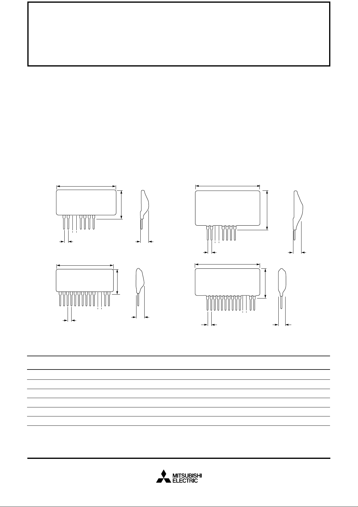
Mitsubishi offers four single in-line
hybrid ICs for driving IGBT
modules. All four drivers are high
speed devices designed to convert
logic level control signals into
optimal IGBT gate drive. Input
signals are isolated from the IGBT
drive using high speed
optocouplers with 15,000V/ms
Figure 5.1 Hybrid IGBT Gate Drivers
35 MAX
M57957L
2.54
23 MAX
10 MAX
common mode noise immunity.
This feature allows convenient
common referencing of high and
low side control signals. Mitsubishi
IGBT drivers are designed to
provide the pulse currents
necessary for high performance
switching applications and to
maintain sufficient off bias to
guarantee ruggedness. Hybrid
IGBT drivers simplify gate drive
M57958L
design by minimizing the number
of components required. In
addition to high performance gate
drive, the M57959L and the
M57962L provide short-circuit
protection. The basic package
outlines of the four Mitsubishi
drivers are shown in Figure 5.1.
Table 5.1 lists the key electrical
characteristics of each hybrid
driver.
51 MAX
29
MAX
10 MAX2.54
43 MAX
M57959L
2.54
All Dimensions in mm.
22 MAX
11 MAX
51 MAX
M57962L
2.54
25
MAX
12 MAX
Table 5.1 Recommended Gate Driver Applications
Optimum Application Range*
Gate Drive Circuit Peak Output Current Short Circuit Protection For 600V IGBT Modules For 1200V/1400V IGBT Modules
M57957L 2 Amps No Up to 100A Up to 50A
M57958L 5 Amps No Up to 400A Up to 200A
M57959L 2 Amps Yes Up to 100A Up to 50A
M57962L 5 Amps Yes Up to 400A Up to 200A
M57958L with Booster** 20 Amps No Up to 600A Up to 1000A
M57962L with Booster** 20 Amps Yes Up to 600A Up to 1000A
*Use RG specified in the switching time section of the IGBT module data sheet.
**See Section 5.10
Sep.1998

MITSUBISHI SEMICONDUCTORS POWER MODULES MOS
USING HYBRID GATE DRIVERS AND GATE DRIVE POWER SUPPLIES
5.1 Output Current Limit
When using hybrid gate drivers
RG must be selected such that the
output current rating (IOP) is not
exceeded. If RG is computed using
Equation 5.1 then IOP will not be
exceeded under any condition.
Equation 5.1
Conservative equation for minimum R
R
G
= (VCC + VEE)/I
G(MIN)
OP
Example:
With VCC = 15V and
-VEE = 10V R
G(MIN)
for
M57958L will be:
RG = (15V + 10V)/5A = 5 ohms
In most applications this limit is
unnecessarily conservative.
Considerably lower values of R
G
can usually be used. The
expression for R
G(MIN)
should be
modified to include the effects of
parasitic inductance in the drive
circuit, IGBT module internal
impedance and the finite switching
speed of the hybrid drivers output
stage. Equation 5.2 is an improved
version of Equation 5.1 for
R
G(MIN)
.
Equation 5.2
Improved equation for R
R
IOP - (RG)
= (VCC + VEE)/
G(MIN)
INT
- φ
G(MIN)
Large IGBT modules that contain
parallel chips have internal gate
resistors that balance the gate
drive and prevent internal
oscillations. The parallel
combination of these internal
resistors is R
G(INT)
. R
G(INT)
ranges from 0.75 ohm in large
IGBT modules like CM600HA-24H
to 3.0 ohms in smaller modules like
CM150DY-12H with two parallel
chips. The value of f depends on
the parasitic inductance of the gate
drive circuit and the switching
speed of the hybrid driver. The
exact value of f is difficult to
determine. It is often desirable to
estimate the minimum value of R
G
that can be used with a given
hybrid driver circuit and IGBT
module by monitoring the peak
gate current while reducing R
G
until the rated IOP is reached. The
minimum restriction on RG often
limits the switching performance
and maximum usable operating frequency when large modules
outside of the drivers optimum
application range are being
driven.Further steps to address
this issue are provided in
Section 5.10.
5.2 Power Supply Requirements
Power is usually supplied to hybrid
IGBT gate drivers from low
voltage DC power supplies that
are isolated from the main DC bus
voltage. Isolated power supplies
are required for high side gate
drivers because the emitter
potential of high side IGBTs is
constantly changing. Isolated
power supplies are often desired
for low side IGBT gate drivers in order to eliminate ground loop noise
problems. The gate drive supplies
should have an isolation voltage
rating of at least two times the
IGBTs V
V
= 2400V for 1200V IGBT).
ISO
rating (i.e.
CES
In systems with several isolated
supplies intersupply capacitances
must be minimized in order to
avoid coupling of common mode
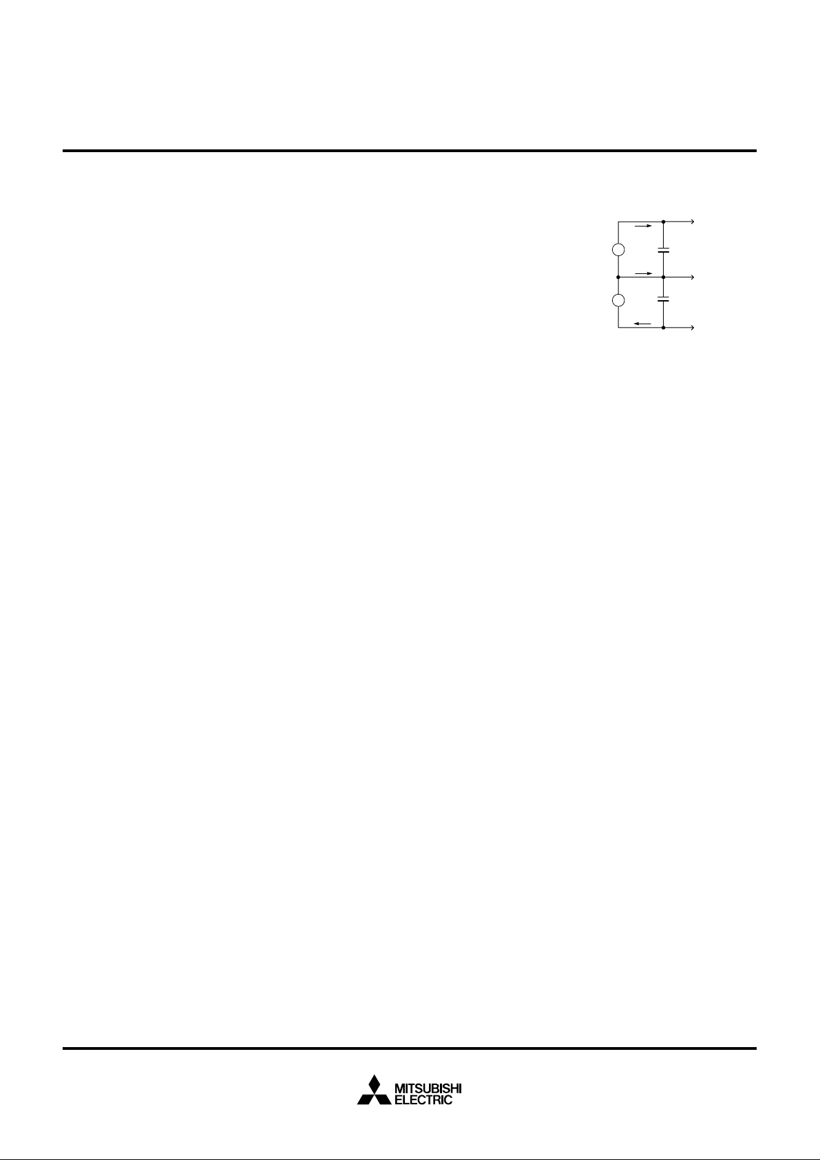
Figure 5.2 Hybrid Driver Power
Supply
I
D
V
(15V)
V
(10V)
+
CC
+
EE
I
COM
+
47µF
+
47µF
I
D
TO HYBRID DRIVER
noise. The recommended power
supply configuration for Mitsubishi
hybrid IGBT gate drivers is shown
in Figure 5.2. Two supplies are
used in order to provide the onand off-bias for the IGBT. The recommended on bias supply (VCC)
voltage is +15V and the recommended off-bias supply voltage
(VEE) is -10V.
Normally these supplies should be
regulated to ±10% however
operation within the range
indicated on the individual driver
data sheets is acceptable.
Electrolytic or tantalum decoupling
capacitors should be connected at
the power supply input pins of the
hybrid driver. These capacitors
supply the high pulse currents
required to drive the IGBT gate.
The amount of capacitance
required depends on the size of the
IGBT module being driven. A 47µF
capacitor is sufficient for most applications.
5.2.1 Supply Current
The current that must be supplied
to the IGBT driver is the sum of two
components. One component is
the quiescent current required to
bias the drivers internal circuits.
The current is constant for fixed
values of VCC and VEE. The second component is the current re-
Sep.1998

MITSUBISHI SEMICONDUCTORS POWER MODULES MOS
USING HYBRID GATE DRIVERS AND GATE DRIVE POWER SUPPLIES
quired to drive the IGBT gate. This
current is directly proportional to
the operating frequency and the total gate charge (QG) of the IGBT
being driven. With small IGBT
modules and at low operating frequencies the quiescent current will
be the dominant component. The
amount of current that must be
supplied to the hybrid driver when
VCC = 15V and VEE = -10V can
be determined from Equations 5.3
and 5.4.
Equation 5.3
Required supply current for
M57957L and M57958L
ID = QG x f
PWM
+ 13mA
Equation 5.4
Required supply current for
M57959L and M57962L
ID = QG x f
PWM
+ 18mA
Where:
ID = Required supply current
QG = Gate charge (See
Section 4.6.3)
f
= Operating frequency
PWM
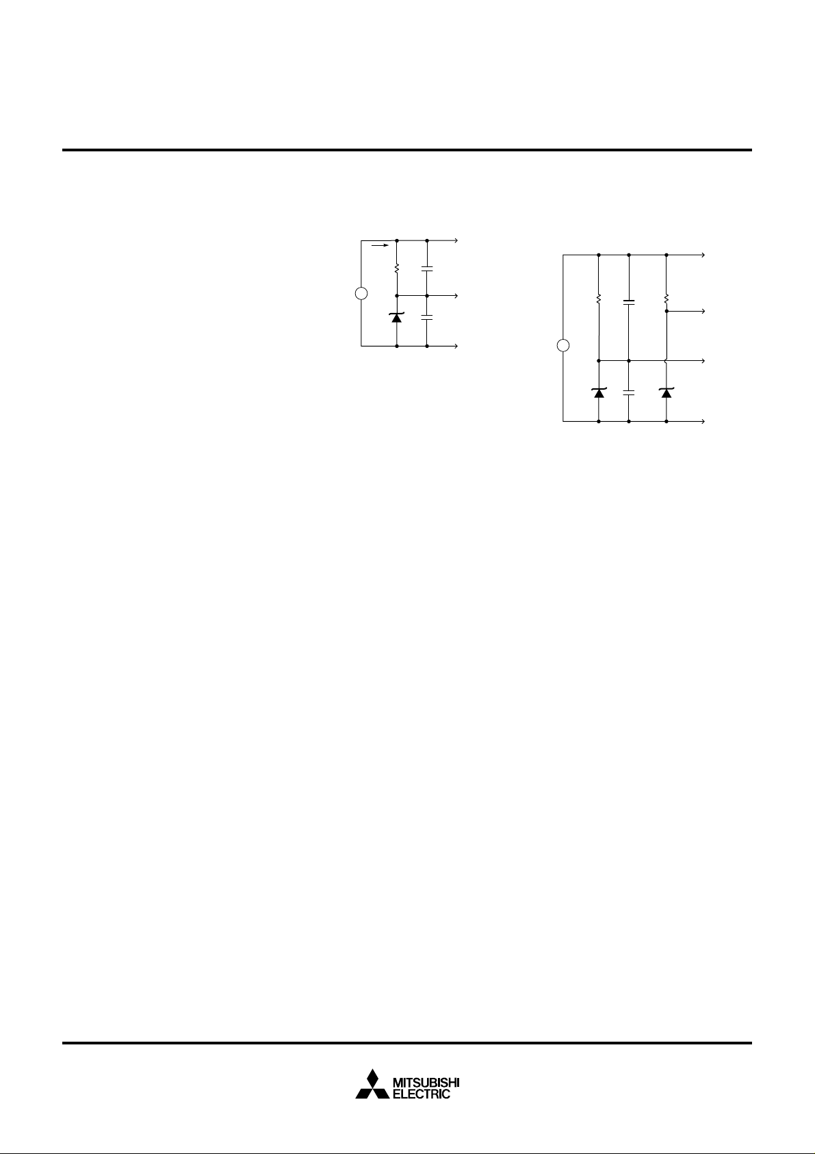
5.2.2 Single Supply Operation
The current drawn from VCC (ID+)
is nearly equal to the current drawn
from VEE (ID-). Only a small
amount of current flows in the common connection (I
COM
). In many
applications it is desirable to operate the hybrid driver from a single
isolated supply. An easy method of
accomplishing this is to create the
common potential using a resistor
and a zener diode. In order to size
the resistor for minimum loss we
must first determine the current
flowing in the common connection
Figure 5.3 Single Supply
Operation of Hybrid
IGBT Drivers
I
D
2.7kΩ
+
V
D
(25V)
(I
). In M57957L and M57958L
COM
10V
+
47µF
+
47µF
TO HYBRID DRIVER
a common connection current of
about 2.5mA is required to bias internal circuits. In M57959L and
M57962L about 3.5mA flows from
the detect pin through the IGBT to
the common connection. The circuit in Figure 5.3 uses a zener supply designed for about 5mA to supply the common current. This circuit allows operation of Mitsubishi
hybrid drivers from a single isolated
25 volt DC supply.
When the power supply circuit
shown in Figure 5.3 is used with
M57957L and M57958L the
required bias voltage at pin 5 of the
hybrid driver appears after a delay
caused by the 2.7kΩ resistor and
the 47µF capacitor. This delay may
cause these drivers to generate an
ON output pulse during power up.
In applications where the main
DC bus voltage is applied before
the gate drive power supplies are
on and stabilized the circuit in Figure 5.4 should be used.
The voltage of the single supply
and the zener diode can be varied
to allow use of standard supplies.
For example, if a 24V DC-to-DC
Figure 5.4 Improved Power
Supply Circuit for
M57957L and
M57958L
TO
HYBRID
DRIVER
2.7kΩ
10V
PIN 6
TO
HYBRID
DRIVER
PIN 5
TO
EMITTER
OF IGBT
TO
HYBRID
DRIVER
PIN 8
V
(25V)
10V
+
47µF
+
47µF
2.7kΩ
+
D
converter is to be used then a 9V
zener diode would give +15/-9
which is acceptable for all of the
hybrid gate drivers. The two
limiting factors that need to be
observed if changes are made are:
(1) Voltages must be within the al-
lowable range specified on the
gate driver data sheet and
(2) The turn on supply should be
15V+/-10% for proper IGBT
performance.
5.3 Total Power Dissipation
The hybrid IGBT driver has a
maximum allowable power
dissipation that is a function of the
ambient temperature. With
VCC = 15V and VEE = -10V the
power dissipated in the driver can
be estimated using Equation 5.5.
Sep.1998
 Loading...