

Mitsubishi M38279EF-XXXFP, M38277M8MXXXHP, M38277M8MXXXGP, M38277M8MXXXFP, M38279EFHP Datasheet
...
MITSUBISHI MICROCOMPUTERS
3827 Group
SINGLE-CHIP 8-BIT CMOS MICROCOMPUTER
DESCRIPTION
The 3827 group is the 8-bit microcomputer based on the 740 family core technology.
The 3827 group has the LCD drive control circuit, the A-D/D-A
converter, the UART, and the PWM as additional functions.
The various microcomputers in the 3827 group include variations
of internal memory size and packaging. For details, refer to the
section on part numbering.
For details on availability of microcomputers in the 3827 group, refer to the section on group expansion.
FEATURES
●Basic machine-language instructions ...................................... 71
●The minimum instruction execution time ........................... 0.5 µs
(at 8MHz oscillation frequency)
●Memory size
ROM ................................................................. 4 K to 60 K bytes
RAM.................................................................192 to 2048 bytes
●Programmable input/output ports ............................................ 55
●Output port ................................................................................. 8
●Input port .................................................................................... 1
●Interrupts ................................................. 17 sources, 16 vectors
(includes key input interrupt)
●Timers ...........................................................8-bit ✕ 3, 16-bit ✕ 2
●Ser ial I/O1 ....................8-bit ✕ 1 (UART or Clock-synchronized)
●Serial I/O2 ...................................8-bit ✕ 1 (Clock-synchronized)
●PWM output .................................................................... 8-bit ✕ 1
●A-D con verter ............................................... 10-bit ✕ 8 channels
●D-A con verter ................................................. 8-bit ✕ 2 channels
●LCD drive control circuit
Bias...................................................................................1/2, 1/3
Duty ........................................................................... 1/2, 1/3, 1/4
Common output.......................................................................... 4
Segment output ........................................................................ 40
●2 Clock generating circuits
(connect to external ceramic resonator or quartz-crystal oscillator)
●Watchdog timer ............................................................ 14-bit ✕ 1
●Power source voltage ................................................ 2.2 to 5.5 V
●Power dissipation
In high-speed mode ..........................................................40 mW
(at 8 MHz oscillation frequency, at 5 V power source voltage)
In low-speed mode............................................................ 60 µW
(at 32 kHz oscillation frequency, at 3 V power source voltage)
●Operating temperature range................................... – 20 to 85°C
APPLICATIONS
Camera, wireless phone, etc.
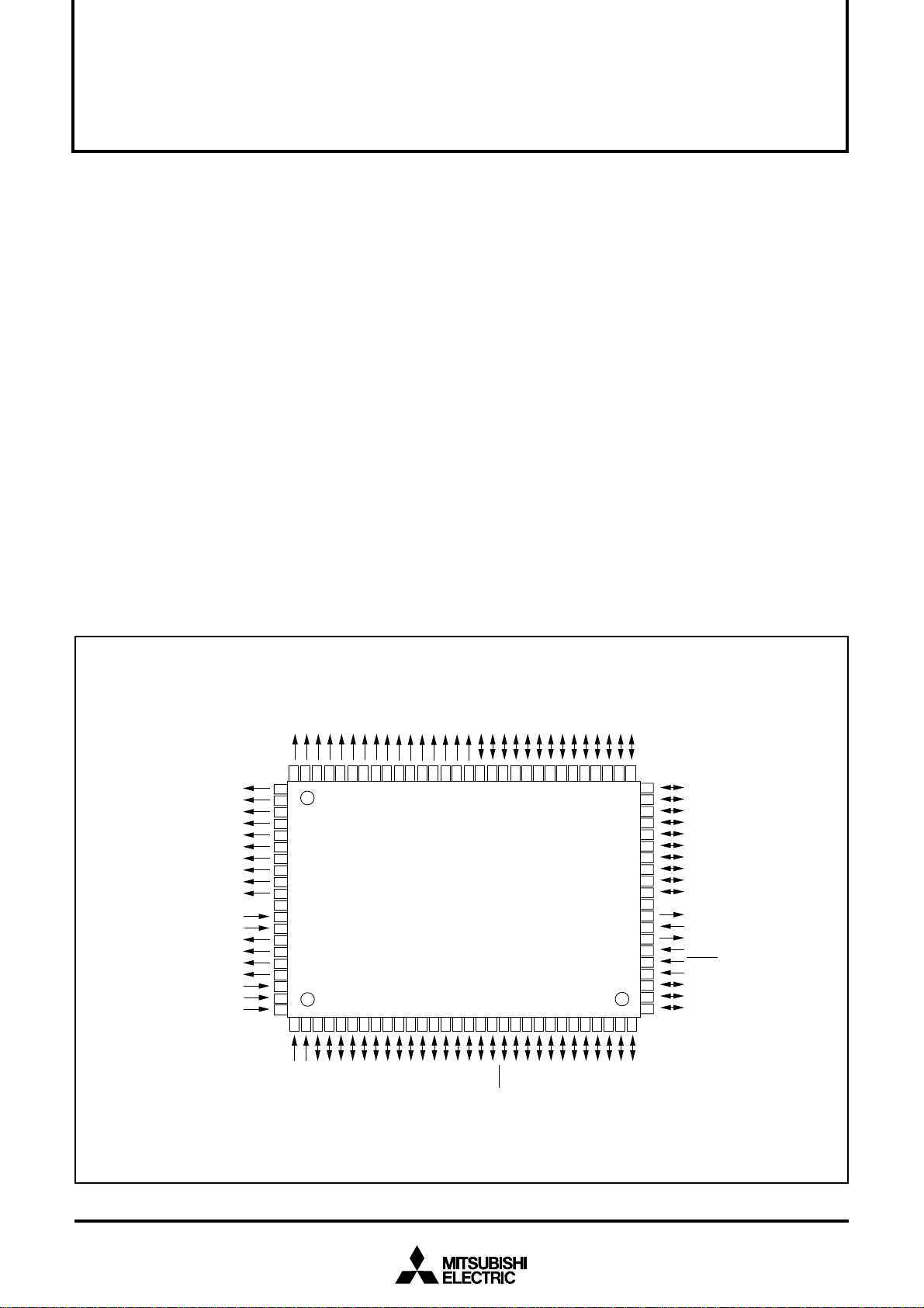
PIN CONFIGURATION (TOP VIEW)
SEG11
SEG14
SEG12
SEG10
SEG13
80
77
79
76
SEG9
SEG8
SEG7
SEG6
SEG5
SEG4
SEG3
SEG2
SEG1
SEG0
VCC
VREF
AVSS
COM3
COM2
COM1
COM0
VL3
VL2
C2
78
81
82
83
84
85
86
87
88
89
90
91
92
93
94
95
96
97
98
99
00
1
2
4
5
3
1
C1
VL1
P65/AN5
P66/AN6
P67/AN7
P34/SEG22
P32/SEG20
P30/SEG18
SEG16
SEG17
SEG15
73
75
72
74
P35/SEG23
P33/SEG21
P31/SEG19
70
71
P36/SEG24
68
67
69
66
P03/SEG29
P01/SEG27
P37/SEG25
P02/SEG28
P00/SEG26
63
65
62
64
61
M38277M8MXXXFP
9
8
6
7
P64/AN4
P61/SOUT2/AN1
P62/SCLK21/AN2
P63/SCLK22/AN3
14
12
11
10
P57/DA2
P60/SIN2/AN0
15
13
P56/DA1
P53/RTP1
P54/CNTR0
P55/CNTR1
20
17
19
16
18
P52/RTP0
P46/SCLK1
P47/SRDY1
P50/PWM0
P51/PWM1
P07/SEG33
P05/SEG31
P06/SEG32
P04/SEG30
58
60
57
59
22
21
23
24
4/RXD
3/φ/TOUT
P45/TXD
P4
P42/INT2
P4
P14/SEG38
P12/SEG36
P10/SEG34
56
25
P41/INT1
P11/SEG35
55
26
P40/ADT
P15/SEG39
P13/SEG37
51
53
52
54
50
P16
49
P17
48
P20
47
P21
46
P22
P23
45
P24
44
P25
43
P26
42
P27
41
VSS
40
XOUT
39
XIN
38
XCOUT
37
XCIN
36
35
RESET
34
P70/INT0
33
P71
P72
32
P73
31
29
30
28
27
7
P76
P7
P74
P75
Package type : 100P6S-A (100-pin plastic-molded QFP)
Fig. 1 M38277M8MXXXFP pin configuration
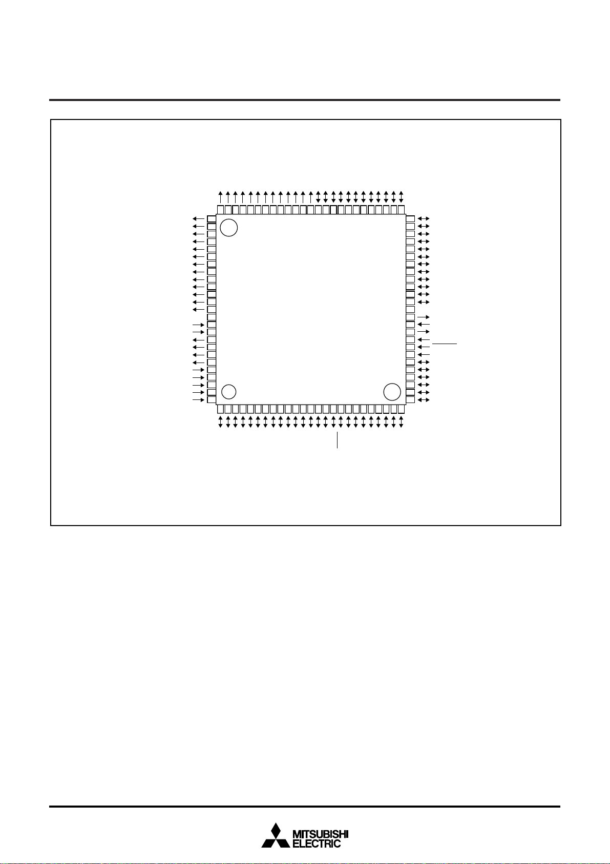
PIN CONFIGURATION (TOP VIEW)
MITSUBISHI MICROCOMPUTERS
3827 Group
SINGLE-CHIP 8-BIT CMOS MICROCOMPUTER
SEG12
SEG11
SEG10
SEG9
SEG8
SEG7
SEG6
SEG5
SEG4
SEG3
SEG2
SEG1
SEG0
VCC
VREF
AVSS
COM3
COM2
COM1
COM0
VL3
VL2
VL1
SEG13
SEG14
73
74
75
76
77
78
79
80
81
82
83
84
85
86
87
88
89
90
91
92
93
94
95
96
97
98
C2
99
C1
100 26
3
2
1
P66/AN6
P67/AN7
P31/SEG19
SEG15
71
72
P33/SEG21
P30/SEG18
SEG17
70
67
68
69
66
M38277M8MXXXGP
M38277M8MXXXHP
6
9
5
8
4
7
10
P64/AN4
P65/AN5
P63/SCLK22/AN3
P57/DA2
P60/SIN2/AN0
P61/SOUT2/AN1
P62/SCLK21/AN2
P32/SEG20
SEG16
P00/SEG26
P02/SEG28
P37/SEG25
P34/SEG22
P36/SEG24
P35/SEG23
64
65
63
13
12
11
P56/DA1
P53/RTP1
P54/CNTR0
P55/CNTR1
P04/SEG30
P01/SEG27
P03/SEG29
61
58
62
59
60
17
16
18
15
14
P52/RTP0
P46/SCLK1
P47/SRDY1
P51/PWM1
P50/PWM0
P05/SEG31
57
19
XD
T
P45/
P12/SEG36
P07/SEG33
P11/SEG35
P06/SEG32
56
21
20
P44/RXD
55
3/φ/TOUT
P4
P13/SEG37
P10/SEG34
52
53
54
51
50
P14/SEG38
49
P15/SEG39
48
P16
47
P17
46
P20
45
P21
44
P22
43
P23
42
P24
41
P25
40
P26
39
P27
38
VSS
37
XOUT
36
XIN
35
COUT
X
34
XCIN
33
RESET
32
P70/INT0
31
P71
30
P72
29
P73
28
P74
27
P75
24
23
22
1/INT1
P40/ADT
P4
P42/INT2
P76
25
7
P7
Package type : GP........ 100P6Q-A (100-pin plastic-molded LQFP)
Package type : HP........ 100PFB-A (100-pin plastic-molded TQFP)
Fig. 2 M38277M8MXXXGP/M38277M8MXXXHP pin configuration
2
Key input/key-on wake-up interrupt
INT1,INT2
CNTR0,CNTR
1
DA
1
DA
2
T
OUT
INT
0
ADT
Data bus
C P U
A
X
Y
S
PC
H
PCL
PS
RESET
V
CC
VSS
Reset input ( 5 V ) ( 0 V )
R O M
R A M
LCD display
RAM
(20 bytes)
I/O port P5
P4(8)
I/O port P4
I/O port P2
P2(8)
I/O port P0
P0(8)
I/O port P1
P1(8)
P6(8)
I/O port P7
P7(8)
Output port P3
P3(8)
I/O port P6
P5(8)
Sub-clock input
Sub-clock output
XCIN XCOUT
Clock generating circuit
X
IN OUT
X
Main clock input
Main clock output
COUT
X
X
CIN
Sub-clock output
Sub-clock input
SI/O1 (8)
VREF
AVSS
A-D converter
(10)
Timer X(16)
Timer Y(16)
Timer 1(8) Timer 2(8)
Timer 3(8)
LCD drive
control circuit
VL1C1C2
VL2
VL3
COM0
COM1
COM2
COM3
SEG0
SEG1
SEG2
SEG3
SEG4
SEG5
SEG6
SEG7
SEG8
SEG9
SEG10
SEG11
SEG12
SEG13
SEG14
SEG15
SEG16
SEG17
φ
X
CIN
COUT
X
SI/O2(8)
Watchdog timer
Reset
PWM(8)
φ
Real time port function
MITSUBISHI MICROCOMPUTERS
3827 Group
SINGLE-CHIP 8-BIT CMOS MICROCOMPUTER
D-A2 D-A1
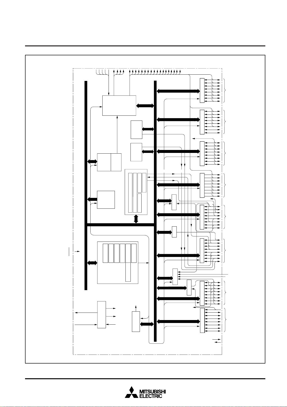
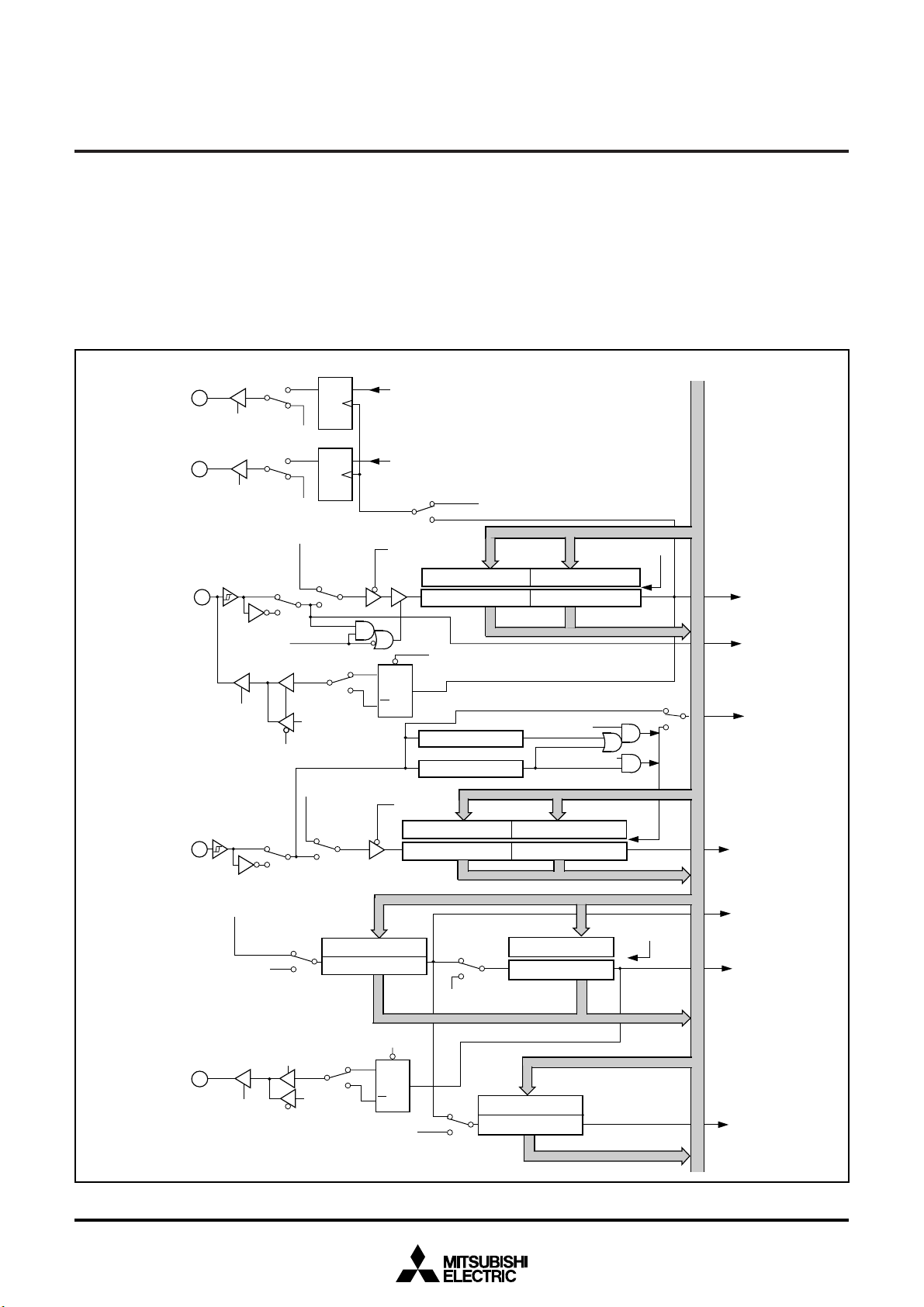
FUNCTIONAL BLOCK DIAGRAM
Fig. 3 Functional block diagram
3
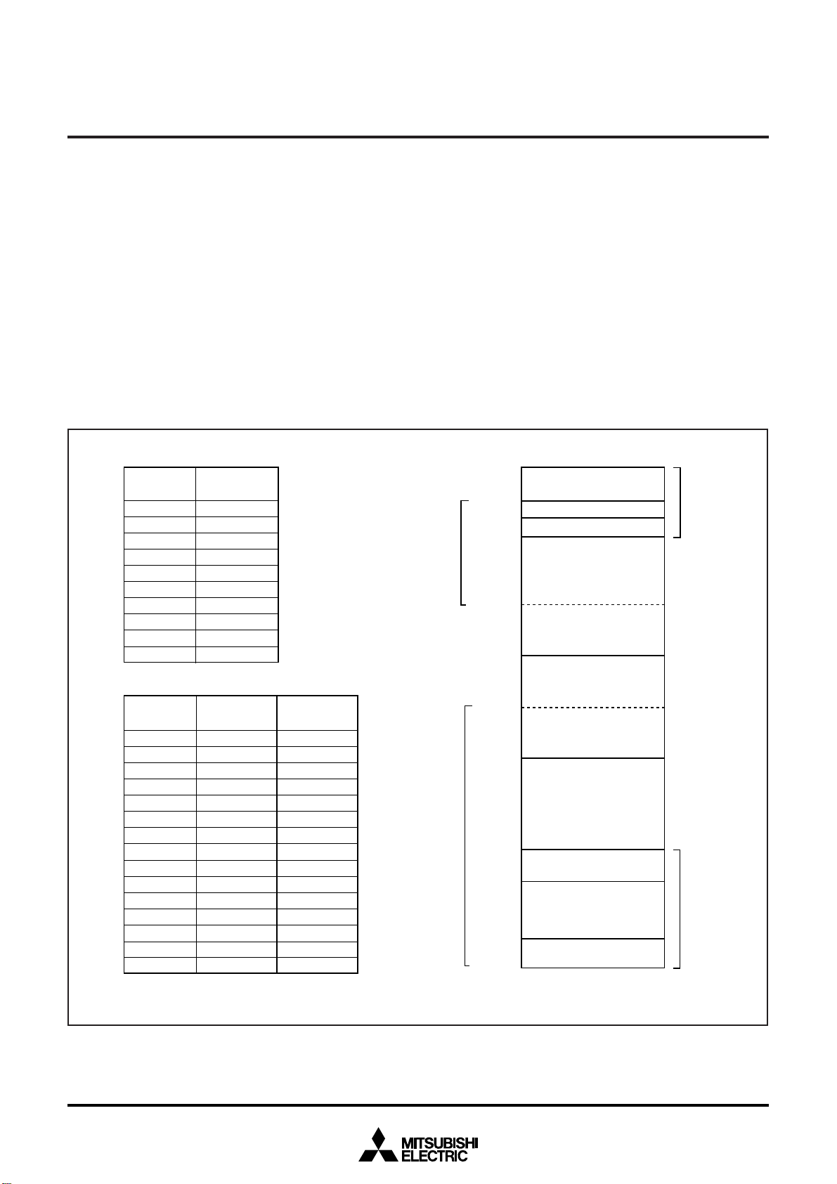
PIN DESCRIPTION
Table 1 Pin description (1)
MITSUBISHI MICROCOMPUTERS
3827 Group
SINGLE-CHIP 8-BIT CMOS MICROCOMPUTER
V
CC, VSS
V
REF
AVSS
RESET
X
IN
XOUT
VL1–VL3
C1, C2
COM0–COM
SEG0–SEG
P00/SEG26–
P07/SEG33
P10/SEG34–
P15/SEG39
P16, P17
P20 – P27
P30/SEG18 –
P37/SEG
25
FunctionPin Name
Power source •Apply voltage of 2.2 V to 5.5 V to VCC, and 0 V to VSS.
Analog refer-
•Reference voltage input pin for A-D converter and D-A converter.
ence voltage
Analog power
source
Reset input
Clock input
•GND input pin for A-D converter and D-A converter.
•Connect to V
SS.
•Reset input pin for active “L”.
•Input and output pins for the main clock generating circuit.
•Connect a ceramic resonator or a quar tz-crystal oscillator between the X
Clock output
LCD power
source
Charge-pump
the oscillation frequency.
•If an external clock is used, connect the clock source to the XIN pin and leave the XOUT pin open.
•Input 0 ≤ V
L1 ≤ VL2 ≤ VL3 ≤ VCC voltage.
•Input 0 – VL3 voltage to LCD.
•External capacitor pins for a voltage multiplier (3 times) of LCD contorl.
capacitor pin
Common output
3
17
Segment output
I/O port P0
•LCD common output pins.
2 and COM3 are not used at 1/2 duty ratio.
•COM
•COM
3 is not used at 1/3 duty ratio.
•LCD segment output pins.
•8-bit output port.
•CMOS compatible input level.
•CMOS 3-state output structure.
•Pull-up control is enabled.
•I/O direction register allows each port to be individually
programmed as either input or output.
I/O port P1
•6-bit output port with same function as por t P0.
•CMOS compatible input level.
•CMOS 3-state output structure.
•Pull-up control is enabled.
•I/O direction register allows each 6-bit pin to be programmed as either input or output.
•2-bit I/O port.
•CMOS compatible input level.
•CMOS 3-state output structure.
•I/O direction register allows each pin to be individually programmed as either input or output.
•Pull-up control is enabled.
I/O port P2
•8-bit I/O port with same function as port P0.
•CMOS compatible input level.
•CMOS 3-state output structure.
•Pull-up control is enabled.
Output port P3
•8-bit output por t with same function as port P0.
•CMOS 3-state output structure.
•Port output control is enabled.
Function except a port function
IN and XOUT pins to set
•LCD segment output pins
•Key input (key-on wake-up) interrupt
input pins
•LCD segment output pins
4
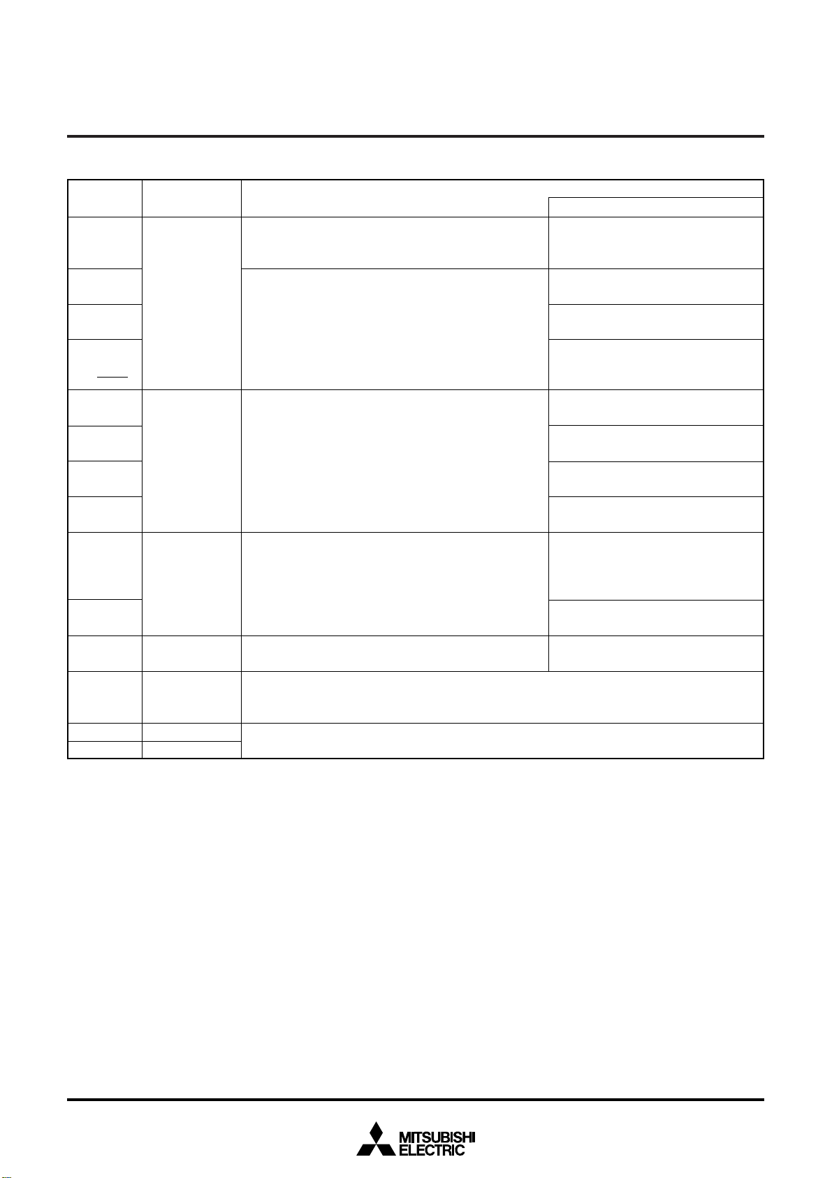
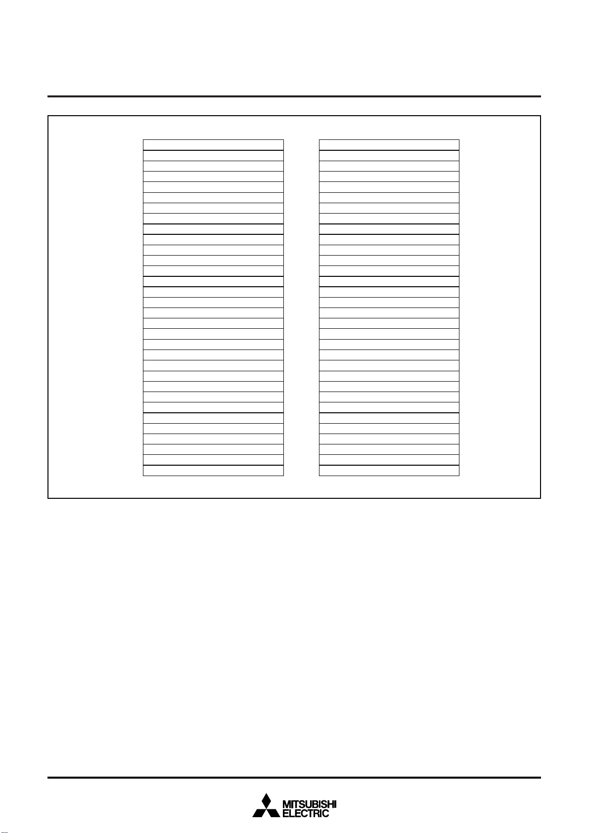
Table 2 Pin description (2)
MITSUBISHI MICROCOMPUTERS
3827 Group
SINGLE-CHIP 8-BIT CMOS MICROCOMPUTER
P40/ADT
P41/INT1,
P42/INT2
P43/φ/TOUT
P44/RXD,
P45/TXD,
P46/SCLK1,
P47/SRDY1
P50/PWM0,
P51/PWM1
P52/RTP0,
P53/RTP1
P54/CNTR0,
P55/CNTR1
P56/DA1,
P57/DA2
P60/AN0/S
IN2,
P61/AN1/S
OUT2,
P62/AN2/S
CLK21,
P63/AN3/S
CLK22
P64/AN4–
P67/AN7
P70/INT0
P71–P77
XCOUT
XCIN
Name
I/O port P4
I/O port P5
I/O port P6
Input port P7
I/O port P7
Sub-clock output
Sub-clock input
FunctionPin
•1-bit I/O port with same function as P16 and P17.
•CMOS compatible input level.
•CMOS 3-state output structure.
•7-bit I/O port with same function as P16 and P17.
•CMOS compatible input level.
•CMOS 3-state output structure.
•Pull-up control is enabled.
•8-bit I/O port with same function as P1
6 and P17.
•CMOS compatible input level.
•CMOS 3-state output structure.
•Pull-up control is enabled.
•8-bit I/O port with same function as P1
6 and P17.
•CMOS compatible input level.
•CMOS 3-state output structure.
•Pull-up control is enabled.
•1-bit I/O port.
•CMOS compatible input level.
•7-bit I/O port with same function as P1
6 and P17.
•CMOS compatible input level.
•N-channel open-drain output structure.
•Sub-clock generating circuit I/O pins.
(Connect a resonator. External clock cannot be used.)
Function except a port function
•A-D trigger input pin
•Interrupt input pin
•Interrupt input pins
•φ clock output pin
•Timer 2 output pin
•Serial I/O1 I/O pins
•PWM function pins
•Real time port function pins
•Timer X, Y function pins
•D-A conversion output pins
•A-D conversion input pins
•Serial I/O2 I/O pins
•A-D conversion input pins
•Interrupt input pin
5
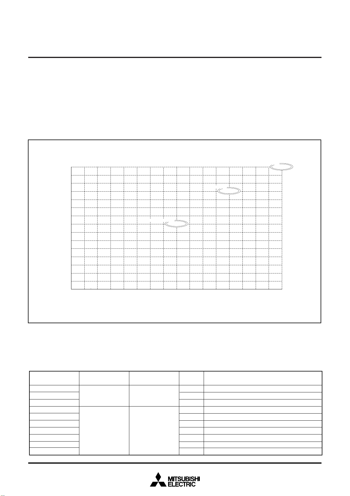
PART NUMBERING
MITSUBISHI MICROCOMPUTERS
3827 Group
SINGLE-CHIP 8-BIT CMOS MICROCOMPUTER
Product
M3827 7 M 8 M XXX HP
Package type
: 100P6S-A package
FP
: 100PFB-A package
HP
: 100P6Q-A package
GP
: 100D0 package
FS
ROM number
Omitted in some types.
Normally, using hyphen
When electrical characteristic, or division of quality
identification code using alphanumeric character.
– : Standard
M : Low power source version
ROM/PROM size
: 4096 bytes
1
2
: 8192 bytes
3
: 12288 bytes
: 16384 bytes
4
5
: 20480 bytes
6
: 24576 bytes
: 28672 bytes
7
8
: 32768 bytes
9
: 36864 bytes
: 40960 bytes
A
B
: 45056 bytes
C
: 49152 bytes
: 53248 bytes
D
E
: 57344 bytes
F
: 61440 bytes
The first 128 bytes and the last 2 bytes of ROM
are reserved areas ; they cannot be used.
Fig. 4 Part numbering
6
Memory type
: Mask ROM version
M
: EPROM or One Time PROM version
E
RAM size
0
: 192 bytes
1
: 256 bytes
2
: 384 bytes
3
: 512 bytes
4
: 640 bytes
5
: 768 bytes
6
: 896 bytes
7
: 1024 bytes
8
: 1536 bytes
9
: 2048 bytes
MITSUBISHI MICROCOMPUTERS
3827 Group
SINGLE-CHIP 8-BIT CMOS MICROCOMPUTER
GROUP EXPANSION
Mitsubishi plans to expand the 3827 group as follows:
Memory Type
Support for Mask ROM, One Time PROM, and EPROM versions
Memory Size
ROM/PROM size ................................................. 4 K to 60 K bytes
RAM size ............................................................192 to 2048 bytes
Memory Expansion Plan
ROM size (bytes)
60K
56K
52K
48K
44K
40K
36K
32K
28K
24K
20K
16K
12K
8K
4K
Under development
Package
100PFB-A ................................0.4 mm-pitch plastic molded TQFP
100P6Q-A ................................0.5 mm-pitch plastic molded LQFP
100P6S-A ................................0.65 mm-pitch plastic molded QFP
100D0 ..................... Window type ceramic LCC (EPROM version)
M38277M8M
Planning
M38278MCM
Under development
M38279EF
256 384 512 640 768 896
192
Note: Products under development or planning: the development schedule and specifications
may be revised without notice.
Fig. 5 Memory expansion plan
Currently supported products are listed below.
Table 3 List of supported products
Product
(P) ROM size (bytes)
ROM size for User in ( )
M38277M8MXXXFP
M38277M8MXXXHP
M38277M8MXXXGP
32768
(32638)
M38279EF-XXXFP
M38279EFFP
M38279EF-XXXHP
M38279EFHP
M38279EF-XXXGP
61440
(61310)
M38279EFGP
M38279EFFS
RAM size (bytes)
RAM size (bytes)
1024
2048
1024
Package
100P6S-A
100PFB-A
100P6Q-A
100P6S-A
100P6S-A
100PFB-A
100PFB-A
100P6Q-A
100P6Q-A
100D0
1408
1536 1664 1792
Remarks
Mask ROM version
Mask ROM version
Mask ROM version
One Time PROM version
One Time PROM version (blank)
One Time PROM version
One Time PROM version (blank)
One Time PROM version
One Time PROM version (blank)
EPROM version
204819201152 1280
As of May 1998
7
MITSUBISHI MICROCOMPUTERS
3827 Group
SINGLE-CHIP 8-BIT CMOS MICROCOMPUTER
FUNCTIONAL DESCRIPTION
Central Processing Unit (CPU)
The 3827 group uses the standard 740 family instruction set. Refer to the table of 740 family addressing modes and machine
instructions or the 740 Family Software Manual for details on the
instruction set.
Machine-resident 740 family instructions are as follows:
The FST and SLW instruction cannot be used.
The STP, WIT, MUL, and DIV instruction can be used.
b7 b0
[CPU Mode Register (CPUM)] 003B16
The CPU mode register contains the stack page selection bit and
the internal system clock selection bit.
The CPU mode register is allocated at address 003B
CPU mode register
(CPUM (CM) : address 003B
Processor mode bits
b1 b0
0 0 : Single-chip mode
0 1 :
1 0 :
1 1 :
Stack page selection bit
0 : 0 page
1 : 1 page
Not used (returns “1” when read)
(Do not write “0” to this bit.)
Port X
0 : Stop oscillating
1 : X
Main clock ( X
0 : Oscillating
1 : Stopped
Main clock division ratio selection bit
0 : X
1 : X
Internal system clock selection bit
0 : X
1 : X
Not available
C
switch bit
CIN
, X
COUT
IN-XOUT
IN
/2 (high-speed mode)
IN
/8 (middle-speed mode)
IN-XOUT
selected (middle-/high-speed mode)
CIN-XCOUT
16
)
) stop bit
selected (low-speed mode)
16.
Fig. 6 Structure of CPU mode register
8
MITSUBISHI MICROCOMPUTERS
3827 Group
SINGLE-CHIP 8-BIT CMOS MICROCOMPUTER
MEMORY
Special Function Register (SFR) Area
The Special Function Register area in the zero page contains control registers such as I/O ports and timers.
RAM
RAM is used for data storage and for stack area of subroutine
calls and interrupts.
ROM
The first 128 bytes and the last 2 bytes of ROM are reserved for
device testing and the rest is user area for storing programs.
Interrupt V ector Area
The interrupt vector area contains reset and interrupt vectors.
RAM area
RAM size
(bytes)
192
256
384
512
640
768
896
1024
1536
2048
ROM area
ROM size
(bytes)
4096
8192
12288
16384
20480
24576
28672
32768
36864
40960
45056
49152
53248
57344
61440
Address
XXXX
00FF
013F16
01BF16
023F16
02BF16
033F16
03BF16
043F16
063F16
083F16
Address
YYYY
F000
E00016
D00016
C00016
B00016
A00016
900016
800016
700016
600016
500016
400016
300016
200016
100016
16
16
16
16
Address
ZZZZ
F08016
E08016
D08016
C08016
B08016
A08016
908016
808016
708016
608016
508016
408016
308016
208016
108016
16
Zero Page
Access to this area with only 2 bytes is possible in the zero page
addressing mode.
Special Page
Access to this area with only 2 bytes is possible in the special
page addressing mode.
000016
SFR area
Zero page
Special page
RAM
ROM
004016
005416
010016
XXXX16
084016
YYYY16
ZZZZ16
FF0016
FFDC16
FFFE16
FFFF16
LCD display RAM area
Reserved area
Not used
Reserved ROM area
(128 bytes)
Interrupt vector area
Reserved ROM area
Fig. 7 Memory map diagram
9
MITSUBISHI MICROCOMPUTERS
3827 Group
SINGLE-CHIP 8-BIT CMOS MICROCOMPUTER
Port P0 (P0)
000016
Port P0 direction register (P0D)
000116
Port P1 (P1)
000216
Port P1 output control register (P1D)
000316
Port P2 (P2)
000416
Port P2 direction register (P2D)
000516
Port P3 (P3)
000616
Port P3 output control register (P3C)
000716
Port P4 (P4)
000816
Port P4 direction register (P4D)
000916
Port P5 (P5)
000A16
Port P5 direction register (P5D)
000B16
Port P6 (P6)
000C16
Port P6 direction register (P6D)
000D16
Port P7 (P7)
000E16
Port P7 direction register (P7D)
000F16
001016
001116
001216
001316
001416
Key input control register (KIC)
001516
PULL register A (PULLA)
001616
PULL register B (PULLB)
001716
Transmit/Receive buffer register(TB/RB)
001816
Serial I/O1 status register (SIO1STS)
001916
Serial I/O1 control register (SIO1CON)
001A16
UART control register (UARTCON)
001B16
Baud rate generator (BRG)
001C16
Serial I/O2 control register (SIO2CON)
001D16
Reserved area
001E16
Serial I/O2 register (SIO2)
001F16
0020
16
Timer X (low) (TXL)
Timer X (high) (TXH)
002116
Timer Y (low) (TYL)
002216
Timer Y (high) (TYH)
002316
002416
Timer 1 (T1)
Timer 2 (T2)
002516
Timer 3 (T3)
002616
Timer X mode register (TXM)
002716
Timer Y mode register (TYM)
002816
Timer 123 mode register (T123M)
002916
OUT/φ output control register (CKCON)
T
002A16
PWM control register (PWMCON)
002B16
PWM prescaler (PREPWM)
002C16
PWM register (PWM)
002D16
002E16
002F16
003016
A-D control register (ADCON)
003116
A-D control register (low-order) (ADL)
003216
A-D control register (high-order) (ADH)
003316
D-A1 conversion register (DA1)
003416
D-A2 conversion register (DA2)
003516
D-A control register (DACON)
003616
Watchdog timer control register (WDTCON)
003716
Segment output enable register (SEG)
003816
LCD mode register (LM)
003916
Interrupt edge selection register (INTEDGE)
003A16
CPU mode register (CPUM)
003B16
Interrupt request register 1(IREQ1)
003C16
Interrupt request register 2(IREQ2)
003D16
Interrupt control register 1(ICON1)
003E16
Interrupt control register 2(ICON2)
003F16
Fig. 8 Memory map of special function register (SFR)
10
I/O PORTS
Direction Registers
The I/O ports have direction registers which determine the input/
output direction of each individual pin. (P0
0–P07 and P10–P15 use
bit 0 of port P0, P1 direction registers respectively.)
When “1” is written to that bit, that pin becomes an output pin.
When “0” is written to the bit corresponding to a pin, that pin becomes an input pin.
If data is read from a pin set to output, the value of the port output
latch is read, not the value of the pin itself. Pins set to input are
floating and the value of that pin can be read. If a pin set to input
is written to, only the port output latch is written to and the pin remains floating.
Port P3 Output Control Register
Bit 0 of the port P3 output control register (address 000716) enables control of the output of ports P3
0 to P37.
When the bit is set to “1”, the port output function is valid.
When resetting, bit 0 of the port P3 output control register is set to
“0” (the port output function is invalid.) and ports P3
0 to P37 are
pulled up.
Pull-up Control
By setting the PULL register A (address 001616) or the PULL register B (address 0017
program.
However, the contents of PULL register A and PULL register B do
not affect ports programmed as the output ports.
The PULL register A setting is invalid for pins set to segment output on the segment output enable register.
16), ports P0 to P6 can control pull-up with a
MITSUBISHI MICROCOMPUTERS
3827 Group
SINGLE-CHIP 8-BIT CMOS MICROCOMPUTER
b7 b0
b7 b0
Note : The contents of PULL register A and PULL register B
do not affect ports programmed as the output port.
Fig. 9 Structure of PULL register A and PULL register B
PULL register A
(PULLA : address 0016
P00, P01 pull-up
P0
2, P03 pull-up
4–P07 pull-up
P0
P1
0–P13 pull-up
4, P15 pull-up
P1
P1
6, P17 pull-up
0–P23 pull-up
P2
P2
4–P27 pull-up
PULL register B
(PULLB : address 0017
P41–P43 pull-up
P4
4–P47 pull-up
0–P53 pull-up
P5
P5
4–P57 pull-up
0–P63 pull-up
P6
P6
4–P67 pull-up
Not used (return “0” when read)
16)
16)
0 : No pull-up
1 : Pull-up
11
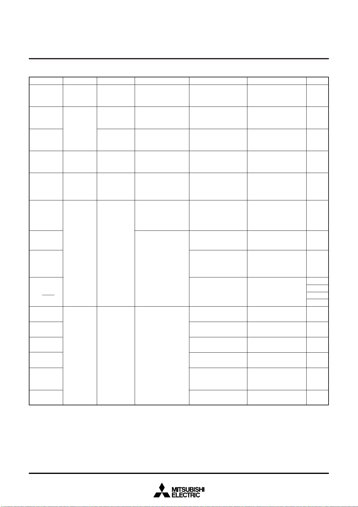
Table 4 List of I/O port function (1)
Pin
P00/SEG26–
P07/SEG33
P10/SEG34–
P15/SEG39
P16 , P17
P20–P27
P30/SEG18–
P37/SEG25
P40/ADT
Port P0
Port P1
Port P2
Port P3
Port P4
Input/OutputName
Input/output,
byte unit
Input/output,
6-bit unit
Input/output,
individual bits
Input/output,
individual bits
Output
Input/output,
individual bits
I/O Format
CMOS compatible
input level
CMOS 3-state output
CMOS compatible
input level
CMOS 3-state output
CMOS compatible
input level
CMOS 3-state output
CMOS compatible
input level
CMOS 3-state output
CMOS 3-state output
CMOS compatible
input level
N-channel open-drain
output
MITSUBISHI MICROCOMPUTERS
3827 Group
SINGLE-CHIP 8-BIT CMOS MICROCOMPUTER
Non-Port Function
LCD segment output
LCD segment output
Key input (key-on
wake-up) interrupt
input
LCD segment output
A-D trigger input
External interrupt input
Related SFRs
PULL register A
Segment output enable
register
PULL register A
Segment output enable
register
PULL register A
PULL register A
Interrupt control register2
Key input control register
PULL register A
Segment output enable
register
P3 output enable register
A-D control register
Interrupt edge selection
register
Diagram No.
(1)
(2)
(1)
(2)
(4)
(4)
(3)
(13)
P4
1/INT1,
P42/INT2
P43/φ/TOUT
P44/RXD,
P45/TXD,
P46/SCLK1,
P47/SRDY1
P50/PWM0,
P51/PWM1
P52/RTP0,
P53/RTP1
P54/CNTR0
P55/CNTR1
P56/DA1
P57/DA2
Port P5
Input/output,
individual bits
CMOS compatible
input level
CMOS 3-state output
CMOS compatible
input level
CMOS 3-state output
External interrupt input
Timer output φ output
Serial I/O1 function I/O
PWM output
Real time port
function output
Timer X function I/O
Timer Y function input
DA1 output
A-D VREF input
DA2 output
PULL register B
Interrupt edge selection
register
PULL register B
Timer 123 mode register
TOUT/φ output control
register
PULL register B
Serial I/O1 control register
Serial I/O1 status register
UART control register
PULL register B
PWM control register
PULL register B
Timer X mode register
PULL register B
Timer X mode register
PULL register B
Timer Y mode register
PULL register B
D-A control register
A-D control register
PULL register B
D-A control register
(4)
(12)
(5)
(6)
(7)
(8)
(10)
(9)
(11)
(14)
(15)
(15)
12
MITSUBISHI MICROCOMPUTERS
SINGLE-CHIP 8-BIT CMOS MICROCOMPUTER
Table 5 List of I/O port function (2)
Pin Name I/O Format Non-Port Function Related SFRS
P60/SIN2/AN0
P61/SOUT2/
AN1
P62/SCLK21/
AN2
P63/SCLK22 /
AN3
P64/AN4–
P67/AN7
P70/INT0
P71–P77
Port P6
Port P7
Input/Output
Input/
output,
individnal
bits
Input
Input/
output,
individnal
bits
CMOS compatible input
level
CMOS 3-state output
CMOS compatible input
level
CMOS compatible input
level
N-channel open-drain
output
A-D conversion input
Serial I/O2 function I/O
A-D conversion input
External interrupt input
A-D control register
Serial I/O2 control
register
A-D control register
Interrupt edge
selection register
3827 Group
Diagram No.
(17)
(18)
(19)
(20)
(16)
(23)
(13)
COM0–COM3
SEG0–SEG17
Notes1: How to use double-function ports as function I/O ports, refer to the applicable sections.
2: Make sure that the input level at each pin is either 0 V or V
tential, a current will flow V
Common
Segment
Output
Output
CC to VSS through the input-stage gate.
LCD common output
LCD segment output
CC during execution of the STP instruction. When an input level is at an intermediate po-
LCD mode register
(21)
(22)
13
MITSUBISHI MICROCOMPUTERS
3827 Group
SINGLE-CHIP 8-BIT CMOS MICROCOMPUTER
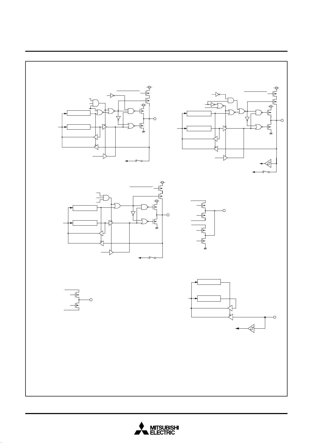
(1) Ports P01–P07, P11–P15
Segment data
Data bus
Port latch
Port direction register
(2) Ports P00, P10
Direction register
Segment data
Data bus
Port latch
(3) Port P3
Segment data
Data bus
Port latch
LCD drive timing
Interface logic level
shift circuit
Port/Segment
Port direction register
LCD drive timing
Port/Segment
LCD drive timing
Interface logic level
shift circuit
Port/Segment
Segment/Port
Segment
Interface logic level
shift circuit
Port direction register
Segment/Port
Segment
Output control
Pull-up
VL2/VL3/VCC
V
L1/VSS
Port
Pull-up
Segment/Port
Segment
Pull-up
VL2/VL3/VCC
V
L1/VSS
Port
VL2/VL3/VCC
L1/VSS
V
Port
(4) Ports P16, P17, P2, P41, P42
Direction register
Data bus
Fig. 10 Port block diagram (1)
14
Port latch
Key input interrupt input
1, INT2 interrupt input
INT
Except P1
Pull-up control
6, P17
(5) Port P44
Serial I/O1 enable bit
Reception enable bit
Data bus
Pull-up control
Direction register
Port latch
Serial I/O1 input
(6) Port P45 (7) Port P46
Serial I/O1 clock
selection bit
Serial I/O1 enable bit
Serial I/O1 enable bit
P45/TxD P-channel output disable bit
Serial I/O1 enable bit
Transmission enable bit
Direction register
Pull-up control
Serial I/O1 mode selection bit
MITSUBISHI MICROCOMPUTERS
3827 Group
SINGLE-CHIP 8-BIT CMOS MICROCOMPUTER
Pull-up control
Direction register
Data bus
Port latch
Serial I/O1 output
(8) Port P47
Serial I/O1 mode selection bit
Serial I/O1 enable bit
S
RDY1 output enable bit
Direction register
Data bus Port latch
Serial I/O1 ready output
(10) Ports P50,P51
Direction register
Data bus
Port latch
Pull-up control
Pull-up control
Data bus
Serial I/O1 clock outupt
Port latch
(9) Ports P52, P53
Direction register
Data bus
Real time control bit
Real time port data
(11) Port P54
Data bus
Serial I/O1 clock input
Pull-up control
Port latch
Pull-up control
Direction register
Port latch
PWM function enable bit
PWM output
Fig. 11 Port block diagram (2)
Pulse output mode
Timer output
CNTR0 interrupt input
15
MITSUBISHI MICROCOMPUTERS
3827 Group
SINGLE-CHIP 8-BIT CMOS MICROCOMPUTER
(12) Port P43
TOUT/φ output control
Timer output
TOUT/φ selection bit
(14) Port P55
Data bus
Direction register
Port latchData bus
φ output
Direction register
Port latch
Pull-up control
Pull-up control
(13) Ports P40, P71–P77
Direction register
Data bus
Port latch
Except P71 to P77
(15) Ports P56, P57
Direction register
Data bus
Port latch
A-D trigger input
Pull-up control
CNTR1 interrupt input
(16) Ports P64–P67
Direction register
Data bus Port latch
A-D conversion input
Fig. 12 Port block diagram (3)
Pull-up control
Analog input pin selection bit
Except P5
(17) Port P60
Data bus
D-A conversion output
VREF input switch
7
Direction register
Port latch
A-D conversion input
D-A
1, D-A2 output enable bit
VREF input selection bit
Pull-up control
Serial I/O2 input
Analog input pin selection bit
16
MITSUBISHI MICROCOMPUTERS
3827 Group
SINGLE-CHIP 8-BIT CMOS MICROCOMPUTER
(18) Port P61
P61/SOUT2 P-channel output disable bit
Serial I/O2 transmit completion signal
Synchronous clock selection bit
Serial I/O2 port selection bit
Data bus
Direction register
Port latch
Serial I/O2 output
A-D conversion input
(20) Port P63
Synchronous clock selection bit
Synchronous clock output pin selection bit
Serial I/O2 port selection bit
Direction register
Data bus
Port latch
Pull-up control
Analog input pin selection bit
Pull-up control
(19) Port P62
Synchronous clock selection bit
Serial I/O2 port selection bit
Synchronous clock output pin
Data bus
selection bit
Direction register
Port latch
Serial I/O2 clock output
(21) COM0–COM3
VL3
VL2
VL1
Pull-up control
Serial I/O2 clock input
A-D conversion input
The gate input signal of each
transistor is controlled by the
LCD duty ratio and the bias
value.
Analog input pin selection bit
Serial I/O2 clock output
(22) SEG0–SEG17
VL2/VL3
VL1/VSS
Fig. 13 Port block diagram (4)
A-D conversion input
The voltage applied to the sources of
P-channel and N-channel transistors
is the controlled voltage by the bias
value.
Analog input pin selection bit
(23) Port P70
Data bus
VSS
Direction register
Port latch
INT0 input
17
MITSUBISHI MICROCOMPUTERS
3827 Group
SINGLE-CHIP 8-BIT CMOS MICROCOMPUTER
INTERRUPTS
Interrupts occur by seventeen sources: seven external, nine internal, and one software.
Interrupt Control
Each interrupt except the BRK instruction interrupt have both an
interrupt request bit and an interrupt enable bit, and is controlled
by the interrupt disable flag. An interrupt occurs if the corresponding interrupt request and enable bits are “1” and the interrupt
disable flag is “0.” Interrupt enable bits can be set or cleared by
software. Interrupt request bits can be cleared by software, but
cannot be set by software. The BRK instruction interrupt and reset
cannot be disabled with any flag or bit. The I flag disables all interrupts except the BRK instruction interrupt and reset. If several
interrupts requests occurs at the same time the interrupt with highest priority is accepted first.
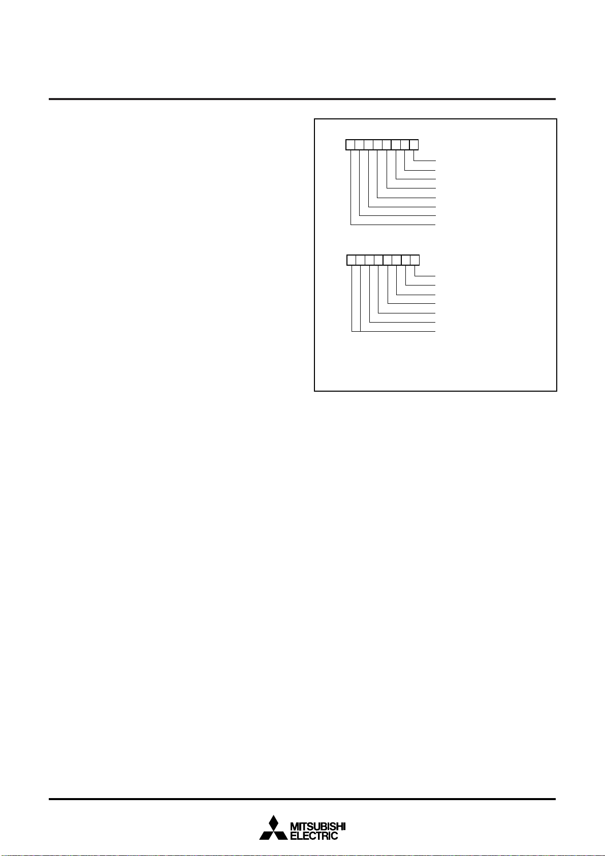
Table 6 Interrupt vector addresses and priority
Interrupt Source
Reset (Note 2)
INT0
INT1
Serial I/O1
reception
Serial I/O1
transmission
Timer X
Timer Y
Timer 2
Timer 3
CNTR
0
CNTR1
Timer 1
INT2
Serial I/O2
Key input
(Key-on wake-up)
ADT
A-D conversion
BRK instruction
Notes1: Vector addresses contain interrupt jump destination addresses.
2: Reset function in the same way as an interrupt with the highest priority.
Prior ity
1
2
3
4
5
6
7
8
9
10
11
12
13
14
15
16
17
Vector Addresses (Note 1)
LowHigh
FFFD
FFFB16
FFF916
FFF716
FFF516
FFF316
FFF116
FFEF16
FFED16
FFEB16
FFE916
FFE716
FFE516
FFE316
FFE116
FFDF16
FFDD16
16
FFFC16
FFFA16
FFF816
FFF616
FFF416
FFF216
FFF016
FFEE16
FFEC16
FFEA16
FFE816
FFE616
FFE416
FFE216
FFE016
FFDE16
FFDC16
Interrupt Operation
Upon acceptance of an interrupt the following operations are automatically performed:
1. The contents of the program counter and processor status
register are automatically pushed onto the stack.
2. The interrupt disable flag is set and the corresponding
interrupt request bit is cleared.
3. The interrupt jump destination address is read from the vector table into the program counter.
■Notes
When the active edge of an external interrupt (INT0–INT2, CNTR0,
CNTR
1) is set or when switching interrupt sources of ADT/A-D
conversion interrupt, the corresponding interrupt request bit may
also be set. Therefore, take following sequence:
(1) Disable the external interrupt which is selected.
(2) Change the active edge in interrupt edge selection register
(timer XY mode register when using CNTR
(3) Clear the set interrupt request bit to “0.”
(4) Enable the external interrupt which is selected.
Interrupt Request
Generating Conditions
At reset
At detection of either rising or
falling edge of INT
At detection of either rising or
falling edge of INT1 input
At completion of serial I/O1 data
reception
At completion of serial I/O1
transmit shift or when transmission buffer is empty
At timer X underflow
At timer Y underflow
At timer 2 underflow
At timer 3 underflow
At detection of either rising or
falling edge of CNTR0 input
At detection of either rising or
falling edge of CNTR
At timer 1 underflow
At detection of either rising or
falling edge of INT
At completion of serial I/O2 data
transmission or reception
At falling of conjunction of input
level for port P2 (at input mode)
At falling of ADT input
At completion of A-D conversion
At BRK instruction execution
0 input
1 input
2 input
Non-maskable
External interrupt
(active edge selectable)
External interrupt
(active edge selectable)
Valid when serial I/O1 is selected
Valid when serial I/O1 is selected
External interrupt
(active edge selectable)
External interrupt
(active edge selectable)
External interrupt
(active edge selectable)
Valid when serial I/O2 is selected
External interrupt
(valid when an “L” level is applied)
Valid when ADT interrupt is selected External interrupt
(Valid at falling)
Valid when A-D interrupt is selected
Non-maskable software interrupt
0, CNTR1)
Remarks
18
Interrupt request bit
Interrupt enable bit
Interrupt disable flag (I)
MITSUBISHI MICROCOMPUTERS
3827 Group
SINGLE-CHIP 8-BIT CMOS MICROCOMPUTER
Fig. 14 Interrupt control
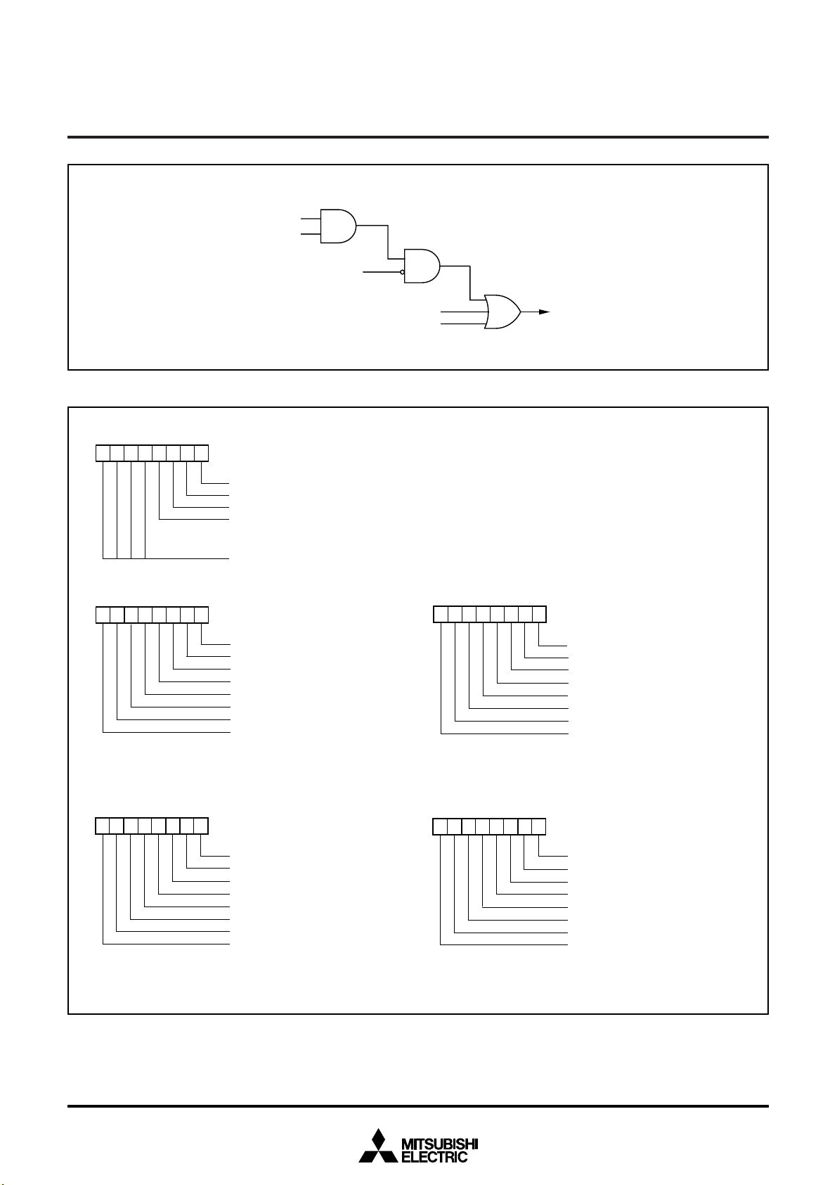
b7 b0
b7 b0
Interrupt edge selection register
16
(INTEDGE : address 003A
)
INT0 interrupt edge selection bit
INT
1
interrupt edge selection bit
2
interrupt edge selection bit
INT
INT
3
interrupt edge selection bit
Not used (return “0” when read)
Interrupt request register 1
(IREQ1 : address 003C
16
)
INT0 interrupt request bit
1
interrupt request bit
INT
Serial I/O1 receive interrupt request bit
Serial I/O1 transmit interrupt request bit
Timer X interrupt request bit
Timer Y interrupt request bit
Timer 2 interrupt request bit
Timer 3 interrupt request bit
BRK instruction
Reset
0 : Falling edge active
1 : Rising edge active
b7 b0
0 : No interrupt request issued
1 : Interrupt request issued
Interrupt request
Interrupt request register 2
(IREQ2 : address 003D
16
)
CNTR0 interrupt request bit
CNTR
1
interrupt request bit
Timer 1 interrupt request bit
INT
2
interrupt request bit
Serial I/O2 interrupt request bit
Key input interrupt request bit
ADT/AD conversion interrupt request bit
Not used (returns “0” when read)
b7 b0
Interrupt control register 1
(ICON1 : address 003E
INT0 interrupt enable bit
1
interrupt enable bit
INT
Serial I/O receive interrupt enable bit
Serial I/O transmit interrupt enable bit
Timer X interrupt enable bit
Timer Y interrupt enable bit
Timer 2 interrupt enable bit
Timer 3 interrupt enable bit
Fig. 15 Structure of interrupt-related registers
b7 b0
16
)
Interrupt control register 2
(ICON2 : address 003F
16
)
CNTR0 interrupt enable bit
1
interrupt enable bit
CNTR
Timer 1 interrupt enable bit
INT
2
interrupt enable bit
Serial I/O2 interrupt enable bit
Key input interrupt enable bit
ADT/AD conversion interrupt enable bit
Not used (returns “0” when read)
(Do not write “1” to this bit.)
0 : Interrupts disabled
1 : Interrupts enabled
19
MITSUBISHI MICROCOMPUTERS
3827 Group
SINGLE-CHIP 8-BIT CMOS MICROCOMPUTER
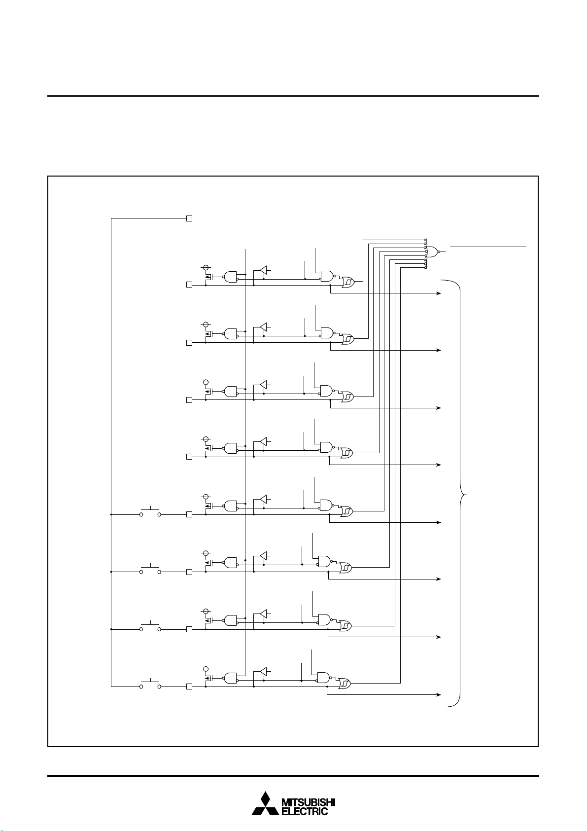
Key Input Interrupt (Key-on wake-up)
A Key-on wake up interrupt request is generated by applying “L”
level to any pin of port P2 that have been set to input mode. In
other words, it is generated when AND of input level goes from “1”
Port PXx
“L” level output
Port P27 output
Port P26 output
Port P25 output
PULLA register
Bit 2 = “1”
✽
✽
✽
Key input control register = “1”
Port P27
direction register = “1”
✽✽
Port P27
latch
Port P26
direction register = “1”
✽✽
Port P26
latch
Port P25
direction register = “1”
✽✽
Port P25
latch
to “0”. An example of using a key input interrupt is shown in Figure
16, where an interrupt request is generated by pressing one of the
keys consisted as an active-low key matrix which inputs to ports
P2
0–P23.
Key input interrupt request
Key input control register = “1”
Key input control register = “1”
Port P24 output
Port P23
input
Port P22
input
Port P21
input
Port P20
input
Key input control register = “1”
Port P24
✽
✽
✽
✽
✽
direction register = “1”
✽✽
Port P24
latch
Port P23
direction register = “0”
Port P22
direction register = “0”
Port P21
direction register = “0”
Port P20
direction register = “0”
Key input control register = “1”
✽✽
Port P23
latch
Key input control register = “1”
✽✽
Port P22
latch
Key input control register = “1”
✽✽
Port P21
latch
Key input control register = “1”
✽✽
Port P20
latch
Port P2 input
reading circuit
Fig. 16 Connection example when using key input interrupt and port P2 block diagram
20
✽ P-channel transistor for pull-up
✽✽ CMOS output buffer
MITSUBISHI MICROCOMPUTERS
3827 Group
SINGLE-CHIP 8-BIT CMOS MICROCOMPUTER
TIMERS
The 3827 group has five timers: timer X, timer Y, timer 1, timer 2,
and timer 3. Timer X and timer Y are 16-bit timers, and timer 1,
timer 2, and timer 3 are 8-bit timers.
All timers are down count timers. When the timer reaches “00
an underflow occurs at the next count pulse and the corresponding timer latch is reloaded into the timer and the count is
continued. When a timer underflows, the interr upt request bit cor-
Real time port
P5
2
P52 direction register
P53
3 direction register
P5
4/CNTR0
P5
P54 direction register
P55/CNTR1
f(XIN)/16
(f(XCIN)/16 in φ = XCIN divided by 2)
P4
3/φ/TOUT
3 direction register
P4
control bit “1”
P5
Real time port
control bit “1”
P5
f(XIN)/16
(f(XIN)/16 in low-speed mode✽)
CNTR
0 active
edge switch bit
“0”
Pulse width
measurement
mode
“1”
CNTR0 active
edge switch bit
Pulse output mode
CNTR1 active
edge switch bit
“0”
“1”
Timer 1 count source
selection bit
XCIN
TOUT output
control bit
f(XIN)/16(f(XCIN)/16 in low-speed mode✽)
Q D
Latch
“0”
2 latch
Q D
“0”
3 latch
Timer X operating mode bits
“00”,“01”,“11”
Latch
Real time port
control bit “0”
“10”
“0”
“1”
4 latch
P5
f(XIN)/16
(f(XCIN)✕16 in φ = XCIN divided by 2)
“00”,“01”,“11”
Timer Y operating
“10”
mode bit
“0”
Timer 1 latch (8)
Timer 1 (8)
“1”
OUT output
T
active edge
switch bit
P4
3 latch
“0”
“1”
T
OUT output
control bit
Q
Q
16”,
2 data for real time port
P5
3 data for real time port
P5
Timer X stop
control bit
Timer X (low) latch (8) Timer X (high) latch (8)
S
Q
T
Q
Rising edge detection
Falling edge detection
Timer Y stop
control bit
Timer Y (low) latch (8) Timer Y (high) latch (8)
Timer Y (low) (8) Timer Y (high) (8)
S
T
Timer 3 count
source selection bit
responding to that timer is set to “1”.
Read and write operation on 16-bit timer must be performed for
both high and low-order bytes. When reading a 16-bit timer, read
the high-order byte first. When writing to a 16-bit timer, write the
low-order byte first. The 16-bit timer cannot perform the correct operation when reading during the write operation, or when writing
during the read operation.
Data bus
Timer X mode register
“1”
Pulse output mode
write signal
Timer X write
control bit
Timer X (low) (8)
Timer X (high) (8)
Timer Y operating mode bit
Pulse width HL continuously measurement mode
Period
measurement mode
Timer 2 count source
selection bit
“0”
Timer 2 latch (8)
Timer 2 (8)
“1”
f(XIN)/16
(f(XCIN)✕16 in φ=XCIN divided by 2)
Timer 3 latch (8)
“0”
Timer 3 (8)
“1”
“00”,“01”,“10”
“11”
Timer 2 write
control bit
Timer Y
interrupt
request
Timer 1
interrupt
request
Timer 2
interrupt
request
Timer 3
interrupt
request
Timer X
interrupt
request
CNTR0
interrupt
request
CNTR1
interrupt
request
Fig. 17 Timer block diagram
21

MITSUBISHI MICROCOMPUTERS
Timer X mode register
(TXM : address 0027
16
)
Timer X write control bit
0 : Write value in latch and counter
1 : Write value in latch only
Real time port control bit
0 : Real time port function invalid
1 : Real time port function valid
P5
2
data for real time port
P5
3
data for real time port
Timer X operating mode bits
b5 b4
0 0 : Timer mode
0 1 : Pulse output mode
1 0 : Event counter mode
1 1 : Pulse width measurement mode
CNTR
0
active edge switch bit
0 : Count at rising edge in event counter mode
Start from “H” output in pulse output mode
Measure “H” pulse width in pulse width
measurement mode
Falling edge active for CNTR
0
interrupt
1 : Count at falling edge in event counter mode
Start from “L” output in pulse output mode
Measure “L” pulse width in pulse width
measurement mode
Rising edge active for CNTR
0
interrupt
Timer X stop control bit
0 : Count start
1 : Count stop
b7 b0
3827 Group
SINGLE-CHIP 8-BIT CMOS MICROCOMPUTER
Timer X
Timer X is a 16-bit timer that can be selected in one of four modes
and can be controlled the timer X write and the real time port by
setting the timer X mode register.
(1) Timer Mode
The timer counts f(XIN)/16 (or f(XCIN)/16 in low-speed mode).
(2) Pulse Output Mode
Each time the timer underflows, a signal output from the CNTR0
pin is inverted. Except for this, the operation in pulse output mode
is the same as in timer mode. When using a timer in this mode, set
the port shared with the CNTR
0 pin to input.
(3) Event Counter Mode
The timer counts signals input through the CNTR0 pin.
Except for this, the operation in event counter mode is the same
as in timer mode. When using a timer in this mode, set the port
shared with the CNTR
0 pin to input.
(4) Pulse Width Measurement Mode
The count source is f(XIN)/16 (or f(XCIN)/16 in low-speed mode). If
CNTR
0 active edge switch bit is “0”, the timer counts while the in-
put signal of CNTR
the input signal of CNTR
mode, set the port shared with tha CNTR
0 pin is at “H”. If it is “1”, the timer counts while
0 pin is at “L”. When using a timer in this
0 pin to input.
■Note on CNTR0 interrupt active edge
selection
CNTR0 interrupt active edge depends on the CNTR0 active edge
switch bit.
●Real time port control
While the real time port function is valid, data for the real time port
are output from ports P5
underflows. (However, if the real time port control bit is changed
from “0” to “1”, data are output without the timer X.) When the data
for the real time port is changed while the real time port function is
valid, the changed data are output at the next underflow of timer X.
Before using this function, set the corresponding port direction
registers to output mode.
2 and P53 each time the timer X
●Timer X write control
If the timer X write control bit is “0”, when the value is written in the
address of timer X, the value is loaded in the timer X and the latch
at the same time.
If the timer X write control bit is “1”, when the value is written in the
address of timer X, the value is loaded only in the latch. The value
in the latch is loaded in timer X after timer X underflows.
If the value is written in latch only, unexpected value may be set in
the high-order counter when the writing in high-order latch and the
underflow of timer X are performed at the same timing.
22
Fig. 18 Structure of timer X mode register

Timer Y
Timer Y mode register
(TYM : address 0028
16)
b7 b0
Not used (return “0” when read)
Timer Y operating mode bits
b5 b4
0 0 : Timer mode
0 1 : Period measurement mode
1 0 : Event counter mode
1 1 : Pulse width HL continuously
measurement mode
CNTR
1 active edge switch bit
0 : Count at rising edge in event counter mode
Measure the falling edge to falling edge
period in period measurement mode
Falling edge active for CNTR
1 interrupt
1 : Count at falling edge in event counter mode
Measure the rising edge period in period
measurement mode
Rising edge active for CNTR
1 interrupt
Timer Y stop control bit
0 : Count start
1 : Count stop
Timer Y is a 16-bit timer that can be selected in one of four modes.
(1) Timer Mode
The timer counts f(XIN)/16 (or f(XCIN)/16 in low-speed mode).
(2) Period Measurement Mode
CNTR1 interrupt request is generated at rising/falling edge of
CNTR
1 pin input signal. Simultaneously, the value in timer Y latch
is reloaded in timer Y and timer Y continues counting down. Except
for the above-mentioned, the operation in period measurement
mode is the same as in timer mode.
The timer value just before the reloading at rising/falling of CNTR
pin input signal is retained until the timer Y is read once after the
reload.
The rising/falling timing of CNTR
CNTR
1 interrupt. When using a timer in this mode, set the port
shared with the CNTR
1 pin to input.
1 pin input signal is found by
MITSUBISHI MICROCOMPUTERS
3827 Group
SINGLE-CHIP 8-BIT CMOS MICROCOMPUTER
1
(3) Event Counter Mode
The timer counts signals input through the CNTR1 pin.
Except for this, the operation in event counter mode is the same
as in timer mode. When using a timer in this mode, set the port
shared with the CNTR
1 pin to input.
(4) Pulse Width HL Continuously Measurement
Mode
CNTR1 interrupt request is generated at both rising and falling
edges of CNTR
1 pin input signal. Except for this, the operation in
pulse width HL continuously measurement mode is the same as in
period measurement mode. When using a timer in this mode , set
the port shared with the CNTR
1 pin to input.
■Note on CNTR1 interrupt active edge selection
CNTR1 interrupt active edge depends on the CNTR1 active edge
switch bit. However, in pulse width HL contin uously measurement
mode, CNTR
falling edges of CNTR
CNTR
1 interrupt request is generated at both rising and
1 pin input signal regardless of the setting of
1 active edge switch bit.
Fig. 19 Structure of timer Y mode register
23

Timer 1, Timer 2, Timer 3
Timer 1, timer 2, and timer 3 are 8-bit timers. The count source for
each timer can be selected by timer 123 mode register. The timer
latch value is not affected by a change of the count source. However, because changing the count source may cause an
inadvertent count down of the timer. Therefore, rewrite the value of
timer whenever the count source is changed.
●Timer 2 write control
If the timer 2 write control bit is “0”, when the value is written in the
address of timer 2, the value is loaded in the timer 2 and the latch
at the same time.
If the timer 2 write control bit is “1”, when the value is written in the
address of timer 2, the value is loaded only in the latch. The value
in the latch is loaded in timer 2 after timer 2 underflows.
●Timer 2 output control
When the timer 2 (T
from the T
OUT pin is output each time timer 2 underflows.
In this case, set the port shared with the T
OUT) is output enabled, an inversion signal
OUT pin to the output.
■Notes on timer 1 to timer 3
When the count source of timer 1 to 3 is changed, the timer counting value may be changed large because a thin pulse is generated
in count input of timer . If timer 1 output is selected as the count
source of timer 2 or timer 3, when timer 1 is written, the counting
value of timer 2 or timer 3 may be changed large because a thin
pulse is generated in timer 1 output.
Therefore, set the value of timer in the order of timer 1, timer 2 and
timer 3 after the count source selection of timer 1 to 3.
MITSUBISHI MICROCOMPUTERS
3827 Group
SINGLE-CHIP 8-BIT CMOS MICROCOMPUTER
b7 b0
Note : Internal clock φ is X
Fig. 20 Structure of timer 123 mode register
Timer 123 mode register
(T123M :address 0029
TOUT output active edge switch bit
0 : Start at “H” output
1 : Start at “L” output
T
OUT/φ output control bit
OUT/φ output disabled
0 : T
1 : T
OUT/φ output enabled
Timer 2 write control bit
0 : Write data in latch and counter
1 : Write data in latch only
Timer 2 count source selection bit
0 : Timer 1 output
1 : f(X
IN)/16
CIN)/16 in low-speed mode)
(or f(X
Timer 3 count source selection bit
0 : Timer 1 output
1 : f(X
IN)/16
CIN)/16 in low-speed mode)
(or f(X
Timer 1 count source selection bit
0 : f(X
IN)/16
(or f(X
CIN)/16 in low-speed mode)
CIN)
1 : f(X
Not used (return “0” when read)
CIN/2 in the low-speed mode.
16)
24

MITSUBISHI MICROCOMPUTERS
3827 Group
SINGLE-CHIP 8-BIT CMOS MICROCOMPUTER
SERIAL I/O
Serial I/O1
Serial I/O1 can be used as either clock synchronous or asynchronous (UART) serial I/O. A dedicated timer (baud rate generator) is
also provided for baud rate generation.
Data bus
Address 0018
Shift clock
Serial I/O1
clock selection bit
Frequency division ratio 1/(n+1)
Baud rate generator
Address 001C
Shift clock
Transmit shift register
Transmit buffer register
Address 0018
Data bus
P44/RXD
P46/S
(f(X
CIN
) in low-speed mode)
P47/S
P4
f(XIN)
RDY1
5/TX
CLK
BRG count source selection bit
F/F
D
Receive buffer register
Receive shift register
1/4
Falling-edge detector
(1) Clock Synchronous Serial I/O Mode
Clock synchronous serial I/O1 can be selected by setting the
mode selection bit of the serial I/O1 control register to “1”.
For clock synchronous serial I/O1, the transmitter and the receiver
must use the same clock. If an internal clock is used, transfer is
started by a write signal to the transmit/receive buffer registers.
16
Clock control circuit
16
Clock control circuit
16
Serial I/O1 control register
Receive buffer full flag (RBF)
Receive interrupt request (RI)
1/4
Transmit interrupt source selection bit
Transmit buffer empty flag (TBE)
Serial I/O1 status register
Address 001A
Transmit shift register shift completion flag (TSC)
Transmit interrupt request (TI)
Address 0019
16
16
Fig. 21 Block diagram of clock synchronous serial I/O1
Transfer shift clock
(1/2 to 1/2048 of the internal
clock, or an external clock)
Serial output T
Serial input R
XD
XD
Receive enable signal SRDY1
Write signal to receive/transmit
buffer register (address 0018
16)
TBE = 0
TBE = 1
TSC = 0
Notes
1 : The transmit interrupt (TI) can be selected to occur either when the transmit buffer register has emptied (TBE=1)
or after the transmit shift operation has ended (TSC=1), by setting the transmit interrupt source selection bit (TIC) of the
serial I/O1 control register.
2 : If data is written to the transmit buffer register when TSC=0, the transmit clock is generated continuously and serial data is
output continuously from the T
3 : The receive interrupt (RI) is set when the receive buffer full flag (RBF) becomes “1” .
XD pin.
Fig. 22 Operation of clock synchronous serial I/O1 function
D7D0 D1 D2 D3 D4 D5 D6
D2
D3 D4 D5 D6
D7D0 D1
RBF = 1
TSC = 1
Overrun error (OE)
detection
25

MITSUBISHI MICROCOMPUTERS
3827 Group
SINGLE-CHIP 8-BIT CMOS MICROCOMPUTER
(2) Asynchronous Serial I/O (UART) Mode
Clock asynchronous serial I/O mode (UART) can be selected by
clearing the serial I/O mode selection bit of the serial I/O1 control
register to “0”.
Eight serial data transfer formats can be selected, and the transfer
formats used by a transmitter and receiver must be identical.
The transmit and receive shift registers each have a buffer regis-
Data bus
(f(X
CIN
) in low-speed mode)
P4
4/RX
P46/S
P4
D
STdetector
CLK
BRG count source selection bit
f(XIN)
1/4
5/TX
D
Address 0018
OE
Character length selection bit
7 bits
8 bits
Serial I/O synchronous clock selection bit
Character length selection bit
16
Receive buffer register
Receive shift register
SP detector
PE FE
Frequency division ratio 1/(n+1)
Baud rate generator
Address 001C
ST/SP/PA generator
Transmit shift register
Transmit buffer register
Data bus
ter, but the two buffers have the same address in memory. Since
the shift register cannot be written to or read from directly, transmit
data is written to the transmit buffer, and receive data is read from
the receive buffer.
The transmit buffer can also hold the next data to be tr ansmitted,
and the receive buffer register can hold a character while the next
character is being received.
Serial I/O1 control register
Receive buffer full flag (RBF)
Receive interrupt request (RI)
Clock control circuit
16
1/16
Address 0018
16
Transmit interrupt source selection bit
Address 001A
1/16
UART control register
Transmit shift register shift completion flag (TSC)
Transmit interrupt request (TI)
Transmit buffer empty flag (TBE)
Serial I/O status register
16
Address 001B
Address 0019
16
16
Fig. 23 Block diagram of UART serial I/O1
Transmit or receive clock
Transmit buffer write signal
TBE=0
TSC=0
TBE=1
Serial output TXD
ST
0
Receive buffer read signal
Serial input R
1 : Error flag detection occurs at the same time that the RBF flag becomes “1” (at 1st stop bit, during reception).
Notes
2 : The transmit interrupt (TI) can be selected to occur when either the TBE or TSC flag becomes “1” by the setting of the transmit interrupt source
selection bit (TIC) of the serial I/O1 control register.
3 : The receive interrupt (RI) is set when the RBF flag becomes “1”.
4 : After data is written to the transmit buffer register when TSC=1, 0.5 to 1.5 cycles of the data shift cycle is necessary until changing to TSC=0.
X
D
ST
Fig. 24 Operation of UART serial I/O1 function
TBE=0
D
1
1 start bit
7 or 8 data bits
1 or 0 parity bit
1 or 2 stop bit (s)
1
TBE=1 TSC=1
STD
D
0
D
SP
RBF=1
STD0D
SP D0D
1
✽
Generated at 2nd bit in 2-stop-bit mode
RBF=0
1
SP
✽
RBF=1
SP
26

[Transmit Buffer/Receive Buffer Register
(TB/RB)] 0018
The transmit buffer register and the receive buffer register are located at the same address. The transmit buffer register is
write-only and the receive buffer register is read-only. If a character bit length is 7 bits, the MSB of data stored in the receive buffer
register is “0”.
16
[Serial I/O1 Status Register (SIO1STS)]
0019
16
The read-only serial I/O1 status register consists of seven flags
(bits 0 to 6) which indicate the operating status of the serial I/O
function and various errors.
Three of the flags (bits 4 to 6) are valid only in UART mode.
The receive buffer full flag (bit 1) is cleared to “0” when the receive
buffer is read.
If there is an error, it is detected at the same time that data is
transferred from the receive shift register to the receive buffer register, and the receive buffer full flag is set. A write to the serial I/O1
status register clears all the error flags OE, PE, FE, and SE. Writing “0” to the serial I/O1 enable bit (SIOE) also clears all the status
flags, including the error flags.
All bits of the serial I/O1 status register are initialized to “0” at reset, but if the transmit enable bit (bit 4) of the serial I/O1 control
register has been set to “1”, the transmit shift register shift completion flag (bit 2) and the transmit buffer empty flag (bit 0) become
“1”.
MITSUBISHI MICROCOMPUTERS
3827 Group
SINGLE-CHIP 8-BIT CMOS MICROCOMPUTER
[Serial I/O1 Control Register (SIO1CON)]
001A
16
The serial I/O1 control register contains eight control bits for the
serial I/O1 function.
[UART Control Register (UARTCON) ]001B16
This is a 5 bit register containing four control bits, which are valid
when UART is selected and set the data format of an data receiver/transfer, and one control bit, which is always valid and sets
the output structure of the P4
5/TXD pin.
[Baud Rate Generator(BRG)] 001616
The baud rate generator determines the baud rate for serial transfer.
The baud rate generator divides the frequency of the count source
by 1/(n + 1), where n is the value written to the baud rate generator.
27

MITSUBISHI MICROCOMPUTERS
3827 Group
SINGLE-CHIP 8-BIT CMOS MICROCOMPUTER
b7 b0
b7 b0
Serial I/O1 status register
(SIO1STS : address 0019
Transmit buffer empty flag (TBE)
0: Buffer full
1: Buffer empty
Receive buffer full flag (RBF)
0: Buffer empty
1: Buffer full
Transmit shift register shift completion flag (TSC)
0: Transmit shift in progress
1: Transmit shift completed
Overrun error flag (OE)
0: No error
1: Overrun error
Parity error flag (PE)
0: No error
1: Parity error
Framing error flag (FE)
0: No error
1: Framing error
Summing error flag (SE)
0: OE U PE U FE =0
1: OE U PE U FE =1
16
)
Not used (returns “1” when read)
UART control register
(UARTCON : address 001B
Character length selection bit (CHAS)
0: 8 bits
1: 7 bits
Parity enable bit (PARE)
0: Parity checking disabled
1: Parity checking enabled
Parity selection bit (PARS)
0: Even parity
1: Odd parity
Stop bit length selection bit (STPS)
0: 1 stop bit
1: 2 stop bits
P4
5/TX
D P-channel output disable bit (POFF)
0: CMOS output (in output mode)
1: N-channel open-drain output (in output mode)
16
)
Not used (return “1” when read)
b7 b0
Serial I/O1 control register
(SIO1CON : address 001A
BRG count source selection bit (CSS)
IN
) (f(X
0: f(X
1: f(X
Serial I/O1 synchronous clock selection bit (SCS)
0: BRG output divided by 4 when clock synchronous serial
I/O is selected.
BRG output divided by 16 when UART is selected.
1: External clock input when clock synchronous serial I/O is
selected.
External clock input divided by 16 when UART is selected.
S
RDY1
0: P4
1: P4
Transmit interrupt source selection bit (TIC)
0: Interrupt when transmit buffer has emptied
1: Interrupt when transmit shift operation is completed
Transmit enable bit (TE)
0: Transmit disabled
1: Transmit enabled
Receive enable bit (RE)
0: Receive disabled
1: Receive enabled
Serial I/O1 mode selection bit (SIOM)
0: Asynchronous serial I/O (UART)
1: Clock synchronous serial I/O
Serial I/O1 enable bit (SIOE)
0: Serial I/O1 disabled
(pins P4
1: Serial I/O1 enabled
(pins P4
CIN
IN
)/4 (f(X
output enable bit (SRDY)
7
pin operates as ordinary I/O pin.
7
pin operates as S
4
–P47 operate as ordinary I/O pins)
4
–P47 operate as serial I/O pins)
16
)
) in low-speed mode)
CIN
)/4 in low-speed mode)
RDY1
output pin.
Fig. 25 Structure of serial I/O1 control registers
28

MITSUBISHI MICROCOMPUTERS
3827 Group
SINGLE-CHIP 8-BIT CMOS MICROCOMPUTER
Serial I/O2
The serial I/O2 function can be used only for clock synchronous
serial I/O.
For clock synchronous serial I/O2 the transmitter and the receiver
must use the same clock. When the internal clock is used, transfer
is started by a write signal to the serial I/O2 register.
When an internal clock is selected as the synchronous clock of the
serial I/O2, either P6
2 or P63 can be selected as an output pin of
the synchronous clock. In this case, the pin that is not selected as
an output pin of the synchronous clock functions as a port.
[Serial I/O2 Control Register (SIO2CON)]
001D
16
The serial I/O2 control register contains 8 bits which control various serial I/O2 functions.
b7
b0
Serial I/O2 control register
(SIO2CON : address 001D16)
Internal synchronous clock select bits
b2 b1 b0
0 0 0: f(XIN)/8 (f(XCIN)/8 in low-speed mode)
0 0 1: f(XIN)/16 (f(XCIN)/16 in low-speed mode)
0 1 0: f(XIN)/32 (f(XCIN)/32 in low-speed mode)
0 1 1: f(XIN)/64 (f(XCIN)/64 in low-speed mode)
1 0 0:
Do not set
1 0 1:
1 1 0: f(XIN)/128 (f(XCIN)/128 in low-speed mode)
1 1 1: f(XIN)/256 (f(XCIN)/256 in low-speed mode)
Serial I/O2 port selection bit
0: I/O port
1: SOUT2,SCLK21/SCLK22 signal output
P61/SOUT2 P-channel output disable bit
0: CMOS output (in output mode)
1: N-channel open-drain output
(in output mode)
Transfer direction selection bit
0: LSB first
1: MSB first
Synchronous clock selection bit
0: External clock
1: Internal clock
Synchronous clock output pin selection bit
0: SCLK21
1: SCLK22
Fig. 26 Structure of serial I/O2 control register
(f(X
CIN
) in low-speed mode)
P63/S
P62/S
P61/S
f(XIN)
P63 latch
(Note)
(Note)
P62 latch
“0”
“1”
1
latch
P6
“0”
“1”
CLK22
CLK21
OUT2
Serial I/O2 port selection bit
P60/S
IN2
Note: It is selected by the synchronous clock selection bit, the synchronous
clock output pin selection bit, and the serial I/O port selection bit.
Synchronous clock
selection bit
Synchronous circuit
CLK2
S
External clock
Internal synchronous
clock select bits
“1”
1/8
1/16
1/32
1/64
Divider
1/128
1/256
“0”
Serial I/O counter 2 (3)
Serial I/O shift register 2 (8)
Data bus
Serial I/O2
interrupt request
Fig. 27 Block diagram of serial I/O2 function
29

Transfer clock (Note 1)
Serial I/O2 register
write signal
Serial I/O2 output S
Serial I/O2 input SIN2
1: When the internal clock is selected as the transfer clock, the divide ratio can be selected by setting bits 0 to 2 of the serial
Notes
I/O2 control register.
2: When the internal clock is selected as the transfer clock, the S
When the external clock is selected as the transfer clock, a content of the serial I/O shift register is continued to shift
during inputting a transfer clock. The S
OUT2
MITSUBISHI MICROCOMPUTERS
SINGLE-CHIP 8-BIT CMOS MICROCOMPUTER
D2
OUT2 pin does not go to high impedance after transfer completion.
D3 D4 D5 D6
Serial I/O2 interrupt request bit set
OUT2 pin goes to high impedance after transfer completion.
3827 Group
(Note 2)
D7D0 D1
Fig. 28 Timing of serial I/O2 function
30

MITSUBISHI MICROCOMPUTERS
3827 Group
SINGLE-CHIP 8-BIT CMOS MICROCOMPUTER
PULSE WIDTH MODULATION (PWM)
The 3827 group has a PWM function with an 8-bit resolution,
based on a signal that is the clock input X
IN or that clock input di-
vided by 2.
Data Setting
The PWM output pin also functions as ports P50 and P51. Set the
PWM period by the PWM prescaler, and set the period during
which the output pulse is an “H” by the PWM register.
If PWM count source is f(X
is n and the value in the PWM register is m (where n = 0 to 255
and m = 0 to 255) :
PWM period = 255 ✕ (n+1)/f(X
= 51 ✕ (n+1) µs (when X
Output pulse “H” period = PWM period ✕ m/255
IN) and the value in the PWM prescaler
IN)
IN = 5 MHz)
= 0.2 ✕ (n+1) ✕ m µs
(when X
IN = 5 MHz)
PWM Operation
When at least either bit 1 (PWM0 output enable bit) or bit 2 (PWM1
output enable bit) of the PWM control register is set to “1”, operation starts by initializing the PWM output circuit, and pulses are
output starting at an “H”. When one PWM output is enabled and
that the other PWM output is enabled, PWM output which is enabled to output later starts pulse output from halfway.
When the PWM register or PWM prescaler is updated during
PWM output, the pulses will change in the cycle after the one in
which the change was made.
51 ✕ m ✕ (n+1)
PWM output
m: Contents of PWM register
n : Contents of PWM prescaler
T : PWM cycle (when f(X
Fig. 29 Timing of PWM cycle
255
T = [51 ✕ (n+1)] µs
IN
) = 5 MHz)
µs
Data bus
prescaler pre-latch
Count source
selection bit
1/2
“0”
“1”
IN
X
Fig. 30 Block diagram of PWM function
PWM
Transfer control circuit
PWM
prescaler latch
PWM prescaler
PWM
register pre-latch
PWM
register latch
PWM circuit
PWM1 enable bit
PWM0 enable bit
Port P5
6
31

MITSUBISHI MICROCOMPUTERS
3827 Group
SINGLE-CHIP 8-BIT CMOS MICROCOMPUTER
b7
b0
PWM control register
(PWMCON : address 002B16)
Count source selection bit
0:f(X
IN
1:f(X
IN
PWM0 function enable bit
0:PWM
1:PWM0 enabled
PWM
1
function enable bit
0:PWM1 disabled
1:PWM
Not used (return “0” when read)
Fig. 31 Structure of PWM control register
A
PWM
(internal)
stop
T
)
)/2
0
disabled
1
enabled
C
B
B
T
C
T2
=
T2
T
stop
PWM
0
output
PWM1 output
PWM register
write signal
PWM prescaler
write signal
PWM0 function
enable bit
1
function
PWM
enable bit
Port
Port
(Changes from “A” to “B” during “H” period)
(Changes from “T” to “T2” during PWM period)
When the contents of the PWM register or PWM prescaler have changed, the PWM
output will change from the next period after the change.
Port
Port
Fig. 32 PWM output timing when PWM register or PWM prescaler is changed
32

A-D CONVERTER
A-D control register
(ADCON : address 0031
16)
Analog input pin selection bits
0 0 0 : P6
0/SIN2/AN0
0 0 1 : P61/SOUT2/AN1
0 1 0 : P62/SCLK21/AN2
0 1 1 : P63/SCLK22/AN3
1 0 0 : P64/AN4
1 0 1 : P65/AN5
1 1 0 : P66/AN6
1 1 1 : P67/AN7
AD conversion completion bit
0 : Conversion in progress
1 : Conversion completed
V
REF input switch bit
0 : OFF
1 : ON
AD external trigger valid bit
0 : A-D external trigger invalid
1 : A-D external trigger valid
Interrupt source selection bit
0 : Interrupt request at A-D
conversion completed
1 : Interrupt request at ADT
input rising or falling
Reference voltage input selection bit
0 : V
REF
1 : P56/DA1
b7 b0
b7 b0
b9 b8 b7 b6 b5 b4 b3 b2
b7 b0
b9 b8
b7 b0
b7 b6 b5 b4 b3 b2
8-bit read (Read only address 0032
16.)
(Address 0032
16)
10-bit read (Read address 003316 first.)
(Address 0033
16)
(Address 0032
16)
Note: High-order 6 bits of address 0033
16 becomes “0” at reading.
b1 b0
[A-D Conversion Register (AD)] 0035
The A-D conversion register is a read-only register that contains
the result of an A-D conversion. During A-D conversion, do not
read this register.
16
[A-D Control Register (ADCON)] 003416
The A-D control register controls the A-D conversion process. Bits
0 to 2 are analog input pin selection bits. Bit 3 is an A-D conversion completion bit and “0” during A-D conversion, then changes
to “1” when the A-D conversion is completed. Writing “0” to this bit
starts the A-D conversion. Bit 4 controls the transistor which
breaks the through current of the resistor ladder. When bit 5, which
is the AD external trigger valid bit, is set to “1”, A-D conversion is
started even by a rising edge or falling edge of an ADT input. Set
ports which share with ADT pins to input when using an A-D external trigger.
MITSUBISHI MICROCOMPUTERS
3827 Group
SINGLE-CHIP 8-BIT CMOS MICROCOMPUTER
[Comparison V oltage Generator]
The comparison voltage generator divides the voltage between
AV
SS and VREF, and outputs the divided voltages.
[Channel Selector]
The channel selector selects one of the input ports P67/AN7–P60/
AN
0, and inputs it to the comparator.
[Comparator and Control Circuit]
The comparator and control circuit compares an analog input voltage with the comparison voltage and stores the result in the A-D
conversion register. When an A-D conversion is completed, the
control circuit sets the AD conversion completion bit and the AD
interrupt request bit to “1”.
Note that the comparator is constructed linked to a capacitor, so
set f(X
IN) to at least 500 kHz during A-D conversion.
Use a clock divided the main clock X
Data bus
A-D control register
P40/ADT
P6
0/SIN2/AN0
P61/SOUT2/AN1
P62/SCLK21/AN2
P63/SCLK22/AN3
P64/AN4
P65/AN5
P66/AN6
P67/AN7
IN as the internal clock φ.
b7
Channel selector
3
Comparater
Fig. 33 Structure of A-D control register
A-D control register
A-D conversion register
10
Resistor ladder
AVSS
b0
ADT/A-D interrupt request
(H)
A-D conversion register
(L)
VREF
P5
6/DA1
Fig. 34 A-D converter block diagram
33

D-A CONVERTER
The 3827 group has an on-chip D-A converter with 8-bit resolution
and 2 channels (DAi (i=1, 2)). The D-A converter is performed by
setting the value in the D-A conversion register. The result of D-A
converter is output from DAi pin. When using the D-A converter,
the corresponding port direction register bit (P5
should be set to “0” (input status).
The output analog voltage V is determined by the value n (base
10) in the D-A conversion register as follows:
V=V
REF ✕ n/256 (n=0 to 255)
Where V
REF is the reference voltage.
At reset, the D-A conversion registers are cleared to “0016”, the
DAi output enable bits are cleared to “0”, and DAi pin goes to
high impedance state. The DA output is not buffered, so connect
an external buffer when driving a low-impedance load.
6/DA1, P57/DA2)
MITSUBISHI MICROCOMPUTERS
SINGLE-CHIP 8-BIT CMOS MICROCOMPUTER
b7
Fig. 35 Structure of D-A control register
b0
D-A control register
(DACON : address 0036
DA1 output enable bit/DA1 VREF
ON/OFF switch
2 output enable bit/DA2 VREF
DA
ON/OFF switch
Not used (return “0” when read)
0 : Output disabled/OFF
1 : Output enabled/ON
3827 Group
16)
V
REF
Internal: D-A output
External: V
Reference voltage input select switch
D-A1 output
(P5
REF
D-A1 output enable switch
D-A1 V
REF
ON/OFF switch
6
)
REF
input
V
ON/OFF switch
R-2R resistor ladder
Data bus
D-A i conversion register (8)
R-2R resistor ladder
D-A1 conversion register (003416)
D-A2 conversion register (0035
Fig. 36 Block diagram of D-A converter
Resistor ladder
D-A1 conversion register (8 bits)
A-D conversion register
(10 bits)
DA i output enable bit
P5
6
/DA
P57/DA
16
)
1
2
D-A2 output enable switch
D-A2 V
REF
ON/OFF switch
D-A2 output
R-2R resistor ladder
(P5
7
)
Fig. 37 A-D converter, D-A converter block diagram
34
D-A2 conversion register (8 bits)

MITSUBISHI MICROCOMPUTERS
3827 Group
SINGLE-CHIP 8-BIT CMOS MICROCOMPUTER
LCD DRIVE CONTROL CIRCUIT
The 3827 group has the built-in Liquid Crystal Display (LCD) drive
control circuit consisting of the following.
●LCD display RAM
●Segment output enable register
●LCD mode register
●Voltage multiplier
●Selector
●Timing controller
●Common driver
●Segment driver
●Bias control circuit
A maximum of 40 segment output pins and 4 common output pins
can be used.
b7 b0
Segment output enable register
(SEG : address 0038
Segment output enable bit 0
0 : Output ports P3
1 : Segment output SEG18–SEG23
Segment output enable bit 1
0 : Output ports P3
1 : Segment output SEG24,SEG25
Segment output enable bit 2
0 : I/O ports P0
1 : Segment output SEG26–SEG31
Segment output enable bit 3
0 : I/O ports P0
1 : Segment output SEG32,SEG33
Segment output enable bit 4
0 : I/O port P1
1 : Segment output SEG34
Segment output enable bit 5
0 : I/O ports P1
1 : Segment output SEG35–SEG39
LCD output enable bit
0 : Disable
1 : Enable
Not used (return “0” when read)
(Do not write “1” to this bit)
Up to 160 pixels can be controlled for LCD display. When the LCD
enable bit is set to “1” after data is set in the LCD mode register,
the segment output enable register and the LCD display RAM, the
LCD drive control circuit starts reading the display data automatically, performs the bias control and the duty ratio control, and
displays the data on the LCD panel.
Table 7 Maximum number of display pixels at each duty ratio
Duty ratio Maximum number of display pixel
2
3
4
16)
0–P35
6, P37
0–P05
6,P07
0
1–P15
80 dots
or 8 segment LCD 10 digits
120 dots
or 8 segment LCD 15 digits
160 dots
or 8 segment LCD 20 digits
b7 b0
Note : LCDCK is a clock for a LCD timing controller.
Fig. 38 Structure of LCD mode register
LCD mode register
(LM : address 0039
Duty ratio selection bits
0 0 : Not used
0 1 : 2 duty (use COM
1 0 : 3 duty (use COM
1 1 : 4 duty (use COM
Bias control bit
0 : 1/3 bias
1 : 1/2 bias
LCD enable bit
0 : LCD OFF
1 : LCD ON
Voltage multiplier control bit
0 : Voltage multiplier disabled
1 : Voltage multiplier enabled
LCD circuit divider division ratio selection bits
0 0 : 1 division of clock input
0 1 : 2 division of clock input
1 0 : 4 division of clock input
1 1 : 8 division of clock input
LCDCK count source selection bit (Note)
0 : f(X
1 : f(X
16)
0, COM1)
0–COM2)
0–COM3)
CIN)/32
IN)/8192 (f(XCIN)/8192 in low-speed mode)
35

Data bus
Timing controller
LCD
divider
f(X
IN
)/8192
f(X
CIN
)/32
COM
0
COM
1
COM
2
COM
3
V
SS
V
L1
V
L2
V
L3
SEG
3
SEG
2
SEG
1
SEG
0
Address 0040
16
Address 0041
16
“0”
“1”
LCDCK
LCDCK count source
selection bit
LCD circuit
divider division
ratio selection bits
Bias control bit
LCD enable bit
Duty ratio selection bits
2
2
Selector Selector Selector Selector
SelectorSelector
LCD display RAM
Address 0053
16
P1
4
/SEG
38
P3
0
/SEG
18
P1
5
/SEG
39
Level
shift
Level
shift
Level
shift
Level
shift
Level
shift
Level
shift
Common
driver
Common
driver
Common
driver
Common
driver
C
1
C
2
Voltage multiplier
control bit
Level
Shift
Level
Shift
Level
Shift
Level
Shift
Segment
driver
Segment
driver
Segment
driver
Segment
driver
Segment
driver
Segment
driver
Bias control
LCD output
enable bit
V
CC
(f(X
CIN
)/8192
in low-speed mode)
MITSUBISHI MICROCOMPUTERS
3827 Group
SINGLE-CHIP 8-BIT CMOS MICROCOMPUTER
Fig. 39 Block diagram of LCD controller/driver
36

MITSUBISHI MICROCOMPUTERS
3827 Group
SINGLE-CHIP 8-BIT CMOS MICROCOMPUTER
VOLTAGE MULTIPLIER (3 TIMES)
The voltage multiplier performs threefold boosting. This circuit inputs a reference voltage for boosting from LCD power input pin
V
L1. (However, when using a 1/2 bias, connect VL1 and V L2 and
apply voltage by external resistor division.)
Set each bit of the segment output enable register and the LCD
mode register in the following order for operating the voltage multiplier.
1. Set the segment output enable bits (bits 0 to 5) of the segment output enable register to “0” or “1.”
2. Set the duty ratio selection bits (bits 0 and 1), the bias control bit (bit 2), the LCD circuit divider division ratio selection
bits (bits 5 and 6), and the LCDCK count source selection
bit (bit 7) of the LCD mode register to “0” or “1.”
3. Set the LCD output enable bit (bit 6) of the segment output
enable register to “1.”
4. Set the voltage multiplier control bit (bit 4) of the LCD mode
register to “1.”
When voltage is input to the V
multiplier, voltage that is twice as large as V
pin, and voltage that is three times as large as VL1 occurs at the
V
L3 pin.
When using the voltage multiplier, apply 1.3 V ≤ Voltage ≤ 2.3 V to
the V
L1 pin.
When not using the voltage multiplier,apply proper voltage to the
LCD power input pins (V
bit to “1.”
When the LCD output enable bit is set to “0,” the V
applied to the V
L3 pin inside of this microcomputer.
The voltage multiplier control bit (bit 4 of the LCD mode register)
controls the voltage multiplier.
L1 pin during operating the voltage
L1 occurs at the VL2
L1–VL3). Then set the LCD output enable
CC voltage is
Bias Control and Applied Voltage to LCD Power Input Pins
To the LCD power input pins (VL1–VL3), apply the voltage shown in
Table 8 according to the bias value.
Select a bias value by the bias control bit (bit 2 of the LCD mode
register).
Table 8 Bias control and applied voltage to VL1–VL3
Bias value
VL3=VLCD
1/3 bias
VL2=2/3 VLCD
VL1=1/3 VLCD
V
1/2 bias
Note 1: VLCD is the maximum value of supplied voltage for the
LCD panel.
L3=VLCD
VL2=VL1=1/2 VLCD
Voltage value
V
L3
V
L2
C
2
C
1
V
L1
1/3 bias
when using the voltage multiplier
Fig. 40 Example of circuit at each bias
Contrast control
V
CC
V
L3
R1
V
L2
C
2
Open
C
1
Open
V
L1
1/3 bias
when not using the voltage multiplier
R2
R3
R1=R2=R3
Contrast control
V
CC
V
L3
R4
V
L2
C
2
Open
C
1
Open
V
L1
R5
PX
X
1/2 bias
R4=R5
37

MITSUBISHI MICROCOMPUTERS
3827 Group
SINGLE-CHIP 8-BIT CMOS MICROCOMPUTER
Common Pin and Duty Ratio Control
The common pins (COM0–COM3) to be used are determined by
duty ratio.
Select duty ratio by the duty ratio selection bits (bits 0 and 1 of the
LCD mode register).
When releasing from reset, the V
CC (VL3) voltage is output from
the common pins.
Table 9 Duty ratio control and common pins used
Duty ratio selection bit
Duty
ratio
Notes1: COM2 and COM3 are open.
2
3
4
2: COM
Bit 1 Bit 0
0
1
1
3 is open.
1
0
1
Common pins used
COM
0, COM1 (Note 1)
COM
0–COM2 (Note 2)
COM
0–COM3
Segment Signal Output Pin
Segment signal output pins are classified into the segment-only
pins (SEG
SEG
Segment signals are output according to the bit data of the LCD
RAM corresponding to the duty ratio. After reset release, a V
(=VL3) voltage is output to the segment-only pins and the seg-
0–SEG17), the segment/output port pins (SEG18–
25), and the segment/I/O port pins (SEG26–SEG39).
CC
ment/output port pins are pulled up to the V
CC (=VL3) voltage in
the high impedance condition. The segment/I/O port pins are set
to input ports, and V
CC (=VL3) is applied to them by pull-up resis-
tor.
LCD Display RAM
Address 004016 to 005316 is the designated RAM for the LCD display. When “1” are written to these addresses, the corresponding
segments of the LCD display panel are turned on.
LCD Drive Timing
The LCDCK timing frequency (LCD drive timing) is generated internally and the frame frequency can be determined with the
following equation;
f(LCDCK) =
Frame frequency =
(frequency of count source for LCDCK)
(divider division ratio for LCD)
f(LCDCK)
(duty ratio)
address
0040
0041
0042
0043
0044
0045
0046
0047
0048
0049
004A
004B
004C
004D
004E
004F
0050
0051
0052
0053
Bit
76 5432 10
16
16
16
16
16
16
16
16
16
16
16
16
16
16
16
16
16
16
16
16
SEG
SEG
SEG
SEG
SEG
SEG
SEG
SEG
SEG
SEG
SEG
SEG
SEG
SEG
SEG
SEG
SEG
SEG
SEG
SEG
COM3 COM2 COM1 COM0
1
3
5
7
9
11
13
15
17
19
21
23
25
27
29
31
33
35
37
39
COM3 COM2 COM1 COM0
SEG
SEG
SEG
SEG
SEG
SEG
SEG
SEG
SEG
SEG
SEG
SEG
SEG
SEG
SEG
SEG
SEG
SEG
SEG
SEG
0
2
4
6
8
10
12
14
16
18
20
22
24
26
28
30
32
34
36
38
Fig. 41 LCD display RAM map
38

Internal signal
LCDCK timing
MITSUBISHI MICROCOMPUTERS
3827 Group
SINGLE-CHIP 8-BIT CMOS MICROCOMPUTER
1/4 duty
COM
COM
COM
COM
SEG
1/3 duty
COM
COM
Voltage level
V
0
1
2
3
0
L3
VL2=V
V
SS
V
L3
V
SS
L1
OFF ON OFF ON
COM
3
COM2COM
0
1
1
COM
COM
0
3
COM
2
COM
1
COM
0
V
L3
VL2=V
L1
V
SS
COM
2
SEG
0
OFFON ON OFF ON OFF
COM
0
COM
1/2 duty
COM
0
COM
1
SEG
0
OFFON OFFON OFFON OFFON
COM
1
COM
Fig. 42 LCD drive waveform (1/2 bias)
V
L3
V
SS
COM
COM
0
COM
2
COM1COM
0
COM
1
COM0COM
0
COM
2
V
L3
VL2=V
L1
V
SS
V
L3
V
SS
1
COM
0
2
COM
1
COM
0
1
39

Internal signal
LCDCK timing
MITSUBISHI MICROCOMPUTERS
3827 Group
SINGLE-CHIP 8-BIT CMOS MICROCOMPUTER
1/4 duty
COM
COM
COM
COM
SEG
1/3 duty
COM
COM
Voltage level
V
L3
V
0
1
2
3
0
L2
V
L1
V
SS
V
L3
V
SS
OFF ON OFF ON
COM
3
COM
2
COM
1
COM
0
1
COM
0
3
COM
2
COM
1
COM
0
V
L3
V
L2
V
L1
V
SS
COM
2
SEG
0
COM
0
1/2 duty
COM
0
COM
1
SEG
0
COM1COM
Fig. 43 LCD drive waveform (1/3 bias)
OFFON ON OFF ON OFF
COM
2
COM
1
COM
COM2COM
0
1
COM
0
COM
OFFON OFFON OFFON OFFON
0
COM
1
COM
COM1COM
0
0
COM
1
COM
V
L3
V
SS
2
V
L3
V
L2
V
L1
V
SS
V
L3
V
SS
0
40

MITSUBISHI MICROCOMPUTERS
3827 Group
SINGLE-CHIP 8-BIT CMOS MICROCOMPUTER
WA TCHDOG TIMER
The watchdog timer gives a mean of returning to the reset status
when a program cannot run on a normal loop (for example, because of a software runaway).
The watchdog timer consists of an 8-bit watchdog timer L and a 6bit watchdog timer H. At reset or writing to the watchdog timer
control register (address 0037
“3FFF
16.” When any data is not written to the watchdog timer con-
trol register (address 0037
stop state. The watchdog timer starts to count down from “3FFF
by writing an optional value into the watchdog timer control register (address 0037
16) and an internal reset occurs at an underflow.
Accordingly, programming is usually performed so that writing to
the watchdog timer control register (address 0037
started before an underflow. The watchdog timer does not function
when an optional value have not written to the watchdog timer
control register (address 0037
the following values are read:
XCIN
Internal
system clock
selection bit
XIN
RESET
Fig. 44 Block diagram of watchdog timer
16), the watchdog timer is set to
16) after reset, the watchdog timer is in
16”
16) may be
16). When address 003716 is read,
“FF16” is set when
watchdog timer is
written to.
“1”
1/16
“0”
Undefined instruction
STP instruction disable bit
STP instruction
IN
Watchdog timer
L (8)
Reset
●value of high-order 6-bit counter
●value of STP instruction disable bit
●value of count source selection bit.
When bit 6 of the watchdog timer control register (address 0037
is set to “0,” the STP instruction is valid. The STP instruction is disabled by rewriting this bit to “1.” At this time, if the STP instruction
is executed, it is processed as an undefined instruction, so that a
reset occurs inside.
This bit cannot be rewritten to “0” by programming. This bit is “0”
immediately after reset.
The count source of the watchdog timer becomes the system
clock φ divided b y 8. The detection time in this case is set to 8.19 s
at X
CIN = 32 kHz and 65.536 ms at XIN = 4 MHz.
However, count source of high-order 6-bit timer can be connected
to a signal divided system clock by 8 directly by writing the bit 7 of
the watchdog timer control register (address 0037
detection time in this case is set to 32 ms at X
256 µs at X
IN = 4 MHz. There is no difference in the detection time
16) to “1.” The
CIN = 32 kHz and
between the middle-speed mode and the high-speed mode.
Data bus
Watchdog timer count
source selection bit
“0”
“1”
Watchdog timer
H (6)
Reset circuit
Reset release time wait
“3F16” is set when
watchdog timer is
written to.
Internal reset
16)
b7
b0
Fig. 45 Structure of watchdog timer control register
f(XIN)
Internal
reset signal
Watchdog timer detection
Fig. 46 Timing of reset output
Watchdog timer register (address 003716)
WDTCON
Watchdog timer H (for read-out of high-order 6 bit)
“3FFF16” is set to the watchdog timer by writing values to this address.
STP instruction disable bit
0 STP instruction enabled
1 : STP instruction disabled
Watchdog timer H count source selection bit
0 : Internal system clock/2048 (f(XIN)/4096)
1 : Internal system clock/8 (f(XIN)/16)
2ms (f(XIN) = 4MHZ)
41

TOUT/φ CLOCK OUTPUT FUNCTION
The internal system clock φ or timer 2 divided by 2 (TOUT output)
can be output from port P4
bit (bit 1) of the timer 123 mode register and the T
control register. Set bit 3 of the port P4 direction register to “1”
when outputting the clock.
3 by setting the TOUT/φ output control
OUT/φ output
MITSUBISHI MICROCOMPUTERS
3827 Group
SINGLE-CHIP 8-BIT CMOS MICROCOMPUTER
b7 b0
b7 b0
OUT/φ output control register
T
(CKOUT : address 002A
16)
TOUT/φ output control bit
0 : φ clock output
1 : T
OUT output
Not used (return “0” when read)
Timer 123 mode register
(T123M : address 0029
OUT output active edge switch bit
T
0 : Start on “H” output
1 : Start on “L” output
T
OUT/φ output control bit
OUT/φ output disable
0 : T
OUT/φ output enable
1 : T
Timer 2 write control bit
0 : Write data in latch and timer
1 : Write data in latch only
Timer 2 count source selection bit
0 : Timer 1 output
1 : f(X
IN)/16
(or f(X
CIN)/16 in low-speed mode
Timer 3 count source selection bit
0 : Timer 1 output
1 : f(X
IN)/16
CIN)/16 in low-speed mode
(or f(X
Timer 1 count source selection bit
0 : f(X
IN)/16
CIN)/16 in low-speed mode
(or f(X
CIN)
1 : f(X
16)
Not used (return “0” when read)
✽
)
✽
)
✽
)
✽ : Internal clock φ is f(X
Fig. 47 Structure of TOUT /φ output-related register
CIN)/2 in low-speed mode.
42

RESET CIRCUIT
(Note)
0.2V
CC
0V
0V
Poweron
VCCRESET
VCC
RESET
Power source
voltage detection
circuit
Power source
voltage
Reset input
voltage
Note : Reset release voltage ; V
CC=VCC(min.)
To reset the microcomputer, RESET pin should be held at an “L”
level for 2 µs or more. Then the RESET pin is retur ned to an “H”
level (the power source voltage should be between V
5.5 V, and the oscillation should be stable), reset is released. After
the reset is completed, the program starts from the address contained in address FFFD
16 (high-order byte) and address FFFC16
(low-order byte). Mak e sure that the reset input voltage is less
than 0.2 V
CC for VCC of VCC (min.).
CC(min.) and
MITSUBISHI MICROCOMPUTERS
3827 Group
SINGLE-CHIP 8-BIT CMOS MICROCOMPUTER
X
IN
φ
RESET
Internal
reset
Address
Data
SYNC
Fig. 49 Reset Sequence
XIN : about 8200 cycles
Notes 1: The frequency relation of f(X
2: The question marks (?) indicate an undefined state that
depends on the previous state.
Fig. 48 Reset Circuit Example
????
IN) and f(φ) is f(XIN) = 8 • f(φ).
FFFC FFFD
ADL
Reset address from
vector table
H, ADL
AD
ADH
43

MITSUBISHI MICROCOMPUTERS
3827 Group
SINGLE-CHIP 8-BIT CMOS MICROCOMPUTER
Port P0 direction register
(1)
Port P1 direction register
(2)
Port P2 direction register
(3)
Port P3 output control register
(4)
Port P4 direction register
(5)
Port P5 direction register
(6)
Port P6 direction register
(7)
Port P7 direction register
(8)
Key input control register
(9)
PULL register A
(10)
PULL register B
(11)
Serial I/O1 status register
(12)
Serial I/O1 control register
(13)
UART control register
(14)
Serial I/O2 control register
(15)
Timer X (low-order)
(16)
Timer X (high-order)
(17)
Timer Y (low-order)
(18)
Timer Y (high-order)
(19)
Timer 1
(20)
Timer 2
(21)
Timer 3
(22)
Timer X mode register
(23)
Timer Y mode register
(24)
Timer 123 mode register
(25)
T
(26)
OUT/
φ
output control register
(27)
PWM control register
Address
0001
000316
000516
000716
000916
000B16
000D16
000F16
001516
001616
001716
001916
001A16
001B16
001D16
002016
002116
002216
002316
002416
002516
002616
002716
002816
002916
002A16
002B16
Register contents
16
16
00
0016
0016
0016
0016
0016
0016
0016
0016
3F16
0016
10000000
0016
11100000
0016
FF16
FF16
FF16
FF16
FF16
0116
FF16
0016
0016
0016
0016
0016
A-D control register
(28)
(29)
A-D conversion register
(low-order)
A-D conversion register
(30)
(high-order)
(31)
D-A1 conversion register
D-A2 conversion register
(32)
(33)
D-A control register
Watchdog timer control register
(34)
(35)
Segment output enable register
LCD mode register
(36)
(37)
Interrupt edge selection register
CPU mode register
(38)
(39)
Interrupt request register 1
Interrupt request register 2
(40)
(41)
Interrupt control register 1
Interrupt control register 2
(42)
(43)
Processor status register
Program counter
(44)
Watchdog timer (high-order)
(45)
(46)
Watchdog timer (low-order)
003116
003216
003316
003416
003516
003616
003716
003816
003916
003A16
003B16
003C16
003D16
003E16
003F16
(PS)
(PC
(PC
H)
L)
Register contentsAddress
0816
XX16
XX16
0016
0016
0016
00111111
0016
0016
0016
01001000
0016
0016
0016
0016
1
Contents of address FFFD16
Contents of address FFFC16
3F16
FF16
✕✕✕✕✕✕✕
Note: The contents of all other register and RAM are undefined after reset, so they must be initialized by software.
✕ : Undefined
Fig. 50 Initial status at reset
44

MITSUBISHI MICROCOMPUTERS
X
CINXCOUT XIN XOUT
C
IN
C
OUT
C
CIN
C
COUT
Rf
Rd
3827 Group
SINGLE-CHIP 8-BIT CMOS MICROCOMPUTER
CLOCK GENERATING CIRCUIT
The 3827 group has two built-in oscillation circuits. An oscillation
circuit can be formed by connecting a resonator between X
X
OUT (XCIN and XCOUT). Use the circuit constants in accordance
with the resonator manufacturer's recommended values. No external resistor is needed between X
resistor exists on-chip. However, an external feed-back resistor is
needed between X
To supply a clock signal exter nally, input it to the X
the X
OUT pin open. The sub-clock XCIN-XCOUT oscillation circuit
cannot directly input clocks that are externally generated. Accordingly, be sure to cause an external resonator to oscillate.
Immediately after poweron, only the X
oscillating, and X
CIN and XCOUT.
CIN and XCOUT pins go to high impedance state.
IN and XOUT since a feed-back
IN pin and make
IN oscillation circuit starts
IN and
Frequency Control
(1) Middle-speed Mode
The internal clock φ is the frequency of XIN divided by 8.
After reset, this mode is selected.
(2) High-speed Mode
The internal clock φ is half the frequency of XIN.
(3) Low-speed Mode
●The internal clock φ is half the frequency of XCIN.
●A low-power consumption operation can be realized by stopping
the main clock X
of the CPU mode register to “1”.
When the main clock X
lation to stabilize by programming.
Note: If you switch the mode between middle/high-speed and low-
speed, stabilize both X
sufficient time is required for the sub-clock to stabilize, especially immediately after poweron and at returning from
stop mode. When switching the mode between middle/highspeed and low-speed, set the frequency on condition that
f(X
IN)>3f(XCIN).
IN in this mode. To stop the main clock, set bit 5
IN is restarted, set enough time for oscil-
IN and XCIN oscillations. The
Oscillation Control
(1) Stop Mode
If the STP instruction is executed, the internal clock φ stops at an
“H” level, and X
timer latch 1 and the timer latch 2 is loaded automatically to the
timer 1 and the timer 2. Thus, a value generated time for stabilizing oscillation should be set to the timer 1 latch and the timer 2
latch (low-order 8 bits for the timer 1, high-order 8 bits for the timer
2) before executing the STP instruction.
Either X
source, and the output of timer 1 is connected to timer 2. The bits
of the timer 123 mode register except bit 4 are cleared to “0,” Set
the timer 1 and timer 2 interrupt enable bits to disabled (“0”) before
executing the STP instruction. Oscillator restarts at reset or when
an external interrupt is received, but the internal clock φ is not supplied to the CPU until timer 2 underflows..This allows timer for the
clock circuit oscillation to stabilize.
IN and XCIN oscillators stop. The value set to the
IN or XCIN divided by 16 is input to timer 1 as count
(2) Wait Mode
If the WIT instruction is executed, the inter nal clock φ stops at an
“H” level. The states of X
fore the executing the WIT instruction. The internal cloc k restarts
at reset or when an interrupt is received. Since the oscillator does
not stop, normal operation can be started immediately after the
clock is restarted.
IN and XCIN are the same as the state be-
Fig. 51 Ceramic resonator circuit
X
X
CIN XCOUT
Rf
Rd
IN XOUT
Open
External oscillation
COUT
circuit
CC
V
V
SS
45
C
CIN
Fig. 52 External clock input circuit
C

MITSUBISHI MICROCOMPUTERS
3827 Group
SINGLE-CHIP 8-BIT CMOS MICROCOMPUTER
XCIN
XIN
XCOUT
XOUT
Middle-/High-speed mode
SRQ
Internal system clock selection bit
Low-speed mode
“0”
Main clock stop bit
“1”
(Note)
1/2
1/4
High-speed mode
or Low-speed mode
Timer 1 count
source selection
bit
“1”
1/2
Main clock division ratio selection bit
Middle-speed mode
“1”
“0”
SRQ
“0”
Timer 1
SRQ
Timer 2 count
source selection
bit
“0”
“1”
Timing φ
(Internal clock)
Timer 2
STP instruction
Reset
Interrupt disable flag I
Interrupt request
Note: When selecting the X
C oscillation, set the port XC switch bit to “1” .
Fig. 53 Clock generating circuit block diagram
WIT
instruction
STP instruction
46

Reset
Middle-speed mode (f(φ) =1 MHz)
CM7=0(8 MHz selected)
CM
6
=1(Middle-speed)
CM
5
=0(8 MHz oscillating)
CM
4
=0(32 kHz stopped)
“0”
4
CM
“1”
CM
“1”
MITSUBISHI MICROCOMPUTERS
3827 Group
SINGLE-CHIP 8-BIT CMOS MICROCOMPUTER
CM
6
“0”“1”
“0”
4
“0”
6
CM
“1”
“0”
CM
“1”
High-speed mode (f(φ) =4 MHz)
CM7=0(8 MHz selected)
CM
6
=0(High-speed)
CM
5
=0(8 MHz oscillating)
CM
4
=0(32 kHz stopped)
CM
4
6
“1”
“0”
4
CM
“0”
“1”
Middle-speed mode (f(φ) =1 MHz)
CM7=0(8 MHz selected)
CM6=1(Middle-speed)
CM
5
=0(8 MHz oscillating)
CM
4
=1(32 kHz oscillating)
“0”
7
CM
“1”
Low-speed mode (f(φ) =16 kHz)
CM7=1(32 kHz selected)
CM
6
=1(Middle-speed)
CM
5
=0(8 MHz oscillating)
CM4=1(32 kHz oscillating)
“0”
5
CM
“1”
Low-power dissipation
mode (f(φ) =16 kHz)
CM7=1(32 kHz selected)
CM
6
=1(Middle-speed)
CM
5
=1(8 MHz stopped)
CM4=1(32 kHz oscillating)
CM
“1”
CM
6
“0”“1”
High-speed mode (f(φ) =4 MHz)
CM7=0(8 MHz selected)
CM
6
=0(High-speed)
CM
5
=0(8 MHz oscillating)
CM
4
=1(32 kHz oscillating)
“0”
7
CM
“1”
CM
6
“0”“1”
“0”
5
“0”
6
CM
“1”
CM
“0”
6
“1”
6
CM
“0”“1”
Low-speed mode (f(φ) =16 kHz)
CM7=1(32 kHz selected)
CM
6
=0(High-speed)
CM
5
=0(8 MHz oscillating)
CM4=1(32 kHz oscillating)
CM
5
“1”
“0”
5
CM
Low-power dissipation
mode (f(φ) =16 kHz)
CM7=1(32 kHz selected)
CM
6
=0(High-speed)
CM
5
=1(8 MHz stopped)
CM4=1(32 kHz oscillating)
“0”
“1”
b7 b4
CPU mode register
(CPUM : address 003B
4
: Port Xc switch bit
CM
0: I/O port function
1: X
CIN–XCOUT
5
: Main clock (XIN–X
CM
0: Oscillating
1: Stopped
CM
6
: Main clock division ratio selection bit
0: f(X
1: f(X
7
: Internal system clock selection bit
CM
0: X
IN–XOUT
(middle-/high-speed mode)
CIN–XCOUT
1: X
oscillating function
OUT
) stop bit
IN
)/2 (high-speed mode)
IN
)/8 (middle-speed mode)
selected
selected
16
)
(low-speed mode)
1 : Switch the mode by the allows shown between the mode blocks. (Do not switch between the mode directly without an allow.)
Notes
2 : The all modes can be switched to the stop mode or the wait mode and returned to the source mode when the stop mode or the wait mode is ended.
3 : Timer and LCD operate in the wait mode.
4 : When the stop mode is ended, wait time can be set by connecting timer 1 and timer 2 in middle-/high-speed mode.
5 : When the stop mode is ended, wait time can be set by connecting timer 1 and timer 2 in low-speed mode.
6 : Wait until oscillation stabilizes after oscillating the main clock X
7 : The example assumes that 8 MHz is being applied to the X
Fig. 54 State transitions of system clock
IN
before the switching from the low-speed mode to middle-/high-speed mode.
IN
pin and 32 kHz to the X
CIN
pin. φ indicates the internal clock.
47

MITSUBISHI MICROCOMPUTERS
3827 Group
SINGLE-CHIP 8-BIT CMOS MICROCOMPUTER
NOTES ON PROGRAMMING
Processor Status Register
The contents of the processor status register (PS) after a reset are
undefined, except for the interrupt disable flag (I) which is “1”. After a reset, initialize flags which affect program execution.
In particular, it is essential to initialize the index X mode (T) and
the decimal mode (D) flags because of their effect on calculations.
Interrupt
The contents of the interrupt request bits do not change immediately after they have been written. After writing to an interrupt
request register, execute at least one instruction before performing
a BBC or BBS instruction.
Decimal Calculations
• To calculate in decimal notation, set the decimal mode flag (D)
to “1”, then execute an ADC or SBC instruction. After executing
an ADC or SBC instruction, execute at least one instruction before executing a SEC, CLC, or CLD instruction.
• In decimal mode, the values of the negative (N), overflow (V),
and zero (Z) flags are invalid.
Timers
If a value n (between 0 and 255) is written to a timer latch, the frequency division ratio is 1/(n + 1).
Serial I/O
In clock synchronous serial I/O, if the receive side is using an external clock and it is to output the S
enable bit, the receive enable bit, and the S
to “1”.
Serial I/O1 continues to output the final bit from the T
transmission is completed.
In serial I/O2, the S
transmission is completed.
OUT2 pin goes to high impedance state after
RDY signal, set the transmit
RDY output enable bit
XD pin after
A-D Converter
The comparator uses internal capacitors whose charge will be lost
if the clock frequency is too low.
Make sure that f(X
sion.
Do not execute the STP or WIT instruction during an A-D conversion.
IN) is at least 500 kHz during an A-D conver-
Instruction Execution Time
The instruction execution time is obtained by multiplying the frequency of the internal clock φ by the number of cycles needed to
execute an instruction.
The number of cycles required to execute an instruction is shown
in the list of machine instructions.
The frequency of the internal clock φ is half of the X
IN frequency.
Multiplication and Division Instructions
The index mode (T) and the decimal mode (D) flags do not affect
the MUL and DIV instruction.
The execution of these instructions does not change the contents
of the processor status register.
Ports
The contents of the port direction registers cannot be read.
The following cannot be used:
• The data transfer instruction (LDA, etc.)
• The operation instruction when the index X mode flag (T) is “1”
• The addressing mode which uses the value of a direction register as an index
• The bit-test instruction (BBC or BBS, etc.) to a direction register
• The read-modify-write instruction (ROR, CLB, or SEB, etc.) to a
direction register
Use instructions such as LDM and STA, etc., to set the port direction registers.
48

MITSUBISHI MICROCOMPUTERS
3827 Group
SINGLE-CHIP 8-BIT CMOS MICROCOMPUTER
DATA REQUIRED FOR MASK ORDERS
The following are necessary when ordering a mask ROM production:
(1) Mask ROM Order Confirmation Form
(2) Mark Specification Form
(3) Data to be written to ROM, in EPROM form (three identical
copies)
DATA REQUIRED FOR ROM WRITING ORDERS
The following are necessary when ordering a ROM writing:
(1) ROM Writing Confirmation Form
(2) Mark Specification Form
(3) Data to be written to ROM, in EPROM form (three identical
copies)
ROM PROGRAMMING METHOD
The built-in PROM of the blank One Time PROM version and builtin EPROM version can be read or programmed with a
general-purpose PROM programmer using a special programming
adapter. Set the address of PROM programmer in the user ROM
area.
Table 10 Special programming adapter
Package
100PFB-A
100P6Q-A
100P6S-A
100D0
The PROM of the blank One Time PROM version is not tested or
screened in the assembly process and following processes. To ensure proper operation after programming, the procedure shown in
Figure 55 is recommended to verify programming.
Name of Programming Adapter
Under development (PCA4738H-100A)
PCA4738G-100A
PCA4738F-100A
PCA4738L-100A
Programming with PROM
programmer
Screening (Caution)
(150°C for 40 hours)
Verification with
PROM programmer
Functional check in
target device
Caution :
Fig. 55 Programming and testing of One Time PROM version
The screening temperature is far higher
than the storage temperature. Never
expose to 150 °C exceeding 100 hours.
49

MITSUBISHI MICROCOMPUTERS
3827 Group
SINGLE-CHIP 8-BIT CMOS MICROCOMPUTER
ELECTRICAL CHARACTERISTICS
ABSOLUTE MAXIMUM RATINGS
Table 11 Absolute maximum ratings
Symbol Parameter Conditions Ratings Unit
VCC
VI
VI
VI
VI
VI
VI
VI
VI
VO
VO
VO
VO
VO
VO
VO
Pd
Topr
Tstg
Input voltage P00–P07, P10–P17, P20–P27,
P41–P47, P50–P57, P60–P67
Input voltage P40, P71–P77
Input voltage P70
Input voltage VL1
Input voltage VL2
Input voltage VL3
Input voltage C1, C2
Input voltage RESET, XIN
Output voltage C1, C2
Output voltage P00–P07, P10–P15, P30–P37
Output voltage P16, P17, P20–P27, P41–P47,
P50–P57, P60–P67, P80, P81
Output voltage P40, P71–P77
Output voltage VL3
Output voltage VL2, SEG0–SEG17
Output voltage XOUT
Power dissipation
Operating temperature
Storage temperature
All voltages are based on VSS.
Output transistors are cut off.
At output port
At segment output
Ta = 25 °C
–0.3 to 7.0 VPower source voltage
–0.3 to VCC +0.3
–0.3 to 7.0
–0.3 to V
–0.3 to VCC +0.3
–0.3 to VCC +0.3
–0.3 to VCC +0.3
CC +0.3
–0.3 to VL2
VL1 to VL3
VL2 to 7.0
–0.3 to 7.0
–0.3 to 7.0
–0.3 to VCC
–0.3 to VL3
–0.3 to 7.0
–0.3 to 7.0
–0.3 to V
–20 to 85
–40 to 125
L3
300
V
V
V
V
V
V
V
V
V
V
V
V
V
V
V
V
mW
°C
°C
RECOMMENDED OPERATING CONDITIONS
Table 12 Recommended operating conditions (VCC = 2.5 to 5.5 V, Ta = –20 to 85°C, unless otherwise noted)
Symbol Parameter
High-speed mode f(X
VCC
VSS
VREF
AVSS
VIA
IH
V
VIH
VIH
VIH
VIL
VIL
VIL
VIL
Power source voltage
Power source voltage
A-D, D-A conversion reference voltage
Analog power source voltage
Analog input voltage AN
“H” input voltage P00–P07, P10–P17, P40, P43, P45, P47, P50–P53,
“H” input voltage P20–P27, P41, P42, P44, P46, P54, P55, P57, P60,
“H” input voltage
“H” input voltage
“L” input voltage P00–P07, P10–P17, P40, P43, P45, P47, P50–P53,
“L” input voltage P20–P27, P41, P42, P44, P46, P54, P55, P57, P60,
“L” input voltage
“L” input voltage
0–AN7
Middle-speed mode f(XIN) = 8 MHz
Low-speed mode
P56, P61, P64–P67, P71–P77
P62, P63, P70
RESET
XIN
P56, P61, P64–P67, P71–P77
P62, P63, P70
RESET
XIN
IN) = 8 MHz
Min.
4.0
2.2
2.2
2.7
AVSS
0.7 VCC
0.8 VCC
0.8 VCC
0.8 VCC
0
0
0
0
Limits
Typ. Max.
5.0
5.0
5.0
0
VCC+0.3
0
VCC
VCC
VCC
VCC
VCC
0.3 VCC
0.2 VCC
0.2 VCC
0.2 VCC
5.5
5.5
5.5
Unit
V
V
V
V
V
V
V
V
V
V
V
V
V
50

MITSUBISHI MICROCOMPUTERS
3827 Group
SINGLE-CHIP 8-BIT CMOS MICROCOMPUTER
Table 13 Recommended operating conditions (V
Symbol Parameter
ΣIOH(peak)
ΣIOH(peak)
ΣIOL(peak)
ΣIOL(peak)
ΣIOL(peak)
ΣIOH(avg)
ΣIOH(avg)
ΣIOL(avg)
ΣIOL(avg)
ΣIOL(avg)
IOH(peak)
I
OH(peak)
IOL(peak)
IOL(peak)
IOL(peak)
IOH(avg)
IOH(avg)
IOL(avg)
IOL(avg)
IOL(avg)
Notes1: The total output current is the sum of all the currents flowing through all the applicable ports. The total average current is an average value measured
2: The peak output current is the peak current flowing in each port.
3: The average output current is an average value measured over 100 ms.
“H” total peak output current
“H” total peak output current
“L” total peak output current
“L” total peak output current
“L” total peak output current
“H” total aver age output current
“H” total aver age output current
“L” total average output current
“L” total average output current
“L” total average output current
“H” peak output current
“H” peak output current P16, P17, P20–P27, P41–P47, P50–P57, P60–P67
“L” peak output current
“L” peak output current P16, P17, P20–P27, P41–P47, P50–P57, P60–P67
“L” peak output current
“H” average output current
“H” average output current
“L” average output current
“L” average output current P16, P17, P20–P27, P41–P47, P50–P57, P60–P67
“L” average output current
over 100 ms. The total peak current is the peak value of all the currents.
CC = 2.2 to 5.5 V, Ta = –20 to 85° C, unless otherwise noted)
P00–P07, P10–P17, P20–P27, P30–P37 (Note 1)
P41–P47, P50–P57, P60–P67 (Note 1)
P00–P07, P10–P17, P20–P27, P30–P37 (Note 1)
P41–P47, P50–P57, P60–P67 (Note 1)
P40, P71–P77 (Note 1)
P00–P07, P10–P17, P20–P27, P30–P37 (Note 1)
P41–P47, P50–P57, P60–P67 (Note 1)
P00–P07, P10–P17, P20–P27, P30–P37 (Note 1)
P41–P47, P50–P57, P60–P67 (Note 1)
P40, P71–P77 (Note 1)
P00–P07, P10–P15, P30–P37 (Note 2)
(Note 2)
P00–P07, P10–P15, P30–P37 (Note 2)
(Note 2)
P40, P71–P77 (Note 2)
P00–P07, P10–P15, P30–P37 (Note 3)
P16, P17, P20–P27, P41–P47, P50–P57, P60–P67
P00–P07, P10–P15, P30–P37 (Note 3)
(Note 3)
P40, P71–P77 (Note 3)
Min.
Limits
Typ. Max.
–20
–20
–10
–10
–1.0
–5.0
–0.5
–2.5
20
20
80
10
10
40
5.0
10
20
2.5
5.0
10
Unit
mA
mA
mA
mA
mA
mA
mA
mA
mA
mA
mA
mA
mA
mA
mA
mA
mA
mA
mA
mA
51

MITSUBISHI MICROCOMPUTERS
3827 Group
SINGLE-CHIP 8-BIT CMOS MICROCOMPUTER
Table 14 Recommended operating conditions (Mask ROM version) (VCC = 2.2 to 5.5 V, Ta = –20 to 85°C, unless otherwise noted)
Symbol Parameter
f(CNTR0)
f(CNTR1)
Input frequency for timers X and Y
(duty cycle 50%)
(4.0 V ≤ VCC ≤ 5.5 V)
(2.2 V ≤ VCC ≤ 4.0 V)
Test conditions
Min.
High-speed mode
(4.0 V ≤ VCC ≤ 5.5 V)
High-speed mode
(2.2 V ≤ VCC ≤ 4.0 V)
f(X
IN)
Main clock input oscillation frequency
(Note 1)
Middle-speed mode
f(XCIN)
Notes1: When the oscillation frequency has a duty cycle of 50%.
2: When using the microcomputer in low-speed mode, make sure that the sub-clock input oscillation frequency on condition that f(X
Sub-clock input oscillation frequency (Notes 1, 2)
Limits
Typ. Max.
4.0
(10✕VCC
(20✕V
32.768
CIN) < f(XIN)/3.
–4)/9
8.0
–8)/9
8.0
50
CC
Unit
MHz
MHz
MHz
MHz
MHz
kHz
Table 15 Recommended operating conditions (PROM version) (V
Symbol Parameter
f(CNTR0)
f(CNTR1)
Input frequency for timers X and Y
(duty cycle 50%)
CC = 2.5 to 5.5 V, Ta = –20 to 85°C, unless otherwise noted)
Test conditions
Min.
(4.0 V ≤ VCC ≤ 5.5 V)
(2.5 V ≤ V
CC ≤ 4.0 V)
High-speed mode
CC ≤ 5.5 V)
f(X
IN)
Main clock input oscillation frequency
(Note 1)
(4.0 V ≤ V
High-speed mode
(2.5 V ≤ VCC ≤ 4.0 V)
Middle-speed mode
f(XCIN)
Notes1: When the oscillation frequency has a duty cycle of 50%.
2: When using the microcomputer in low-speed mode, make sure that the sub-clock input oscillation frequency on condition that f(X
Sub-clock input oscillation frequency (Notes 1, 2)
Limits
Typ. Max.
(2✕VCC)
(4✕V
32.768
CIN) < f(XIN)/3.
4.0
8.0
8.0
50
–4
CC)
–8
Unit
MHz
MHz
MHz
MHz
MHz
kHz
52

MITSUBISHI MICROCOMPUTERS
SINGLE-CHIP 8-BIT CMOS MICROCOMPUTER
Table 16 Electrical characteristics (VCC =4.0 to 5.5 V, Ta = –20 to 85°C, unless otherwise noted)
Symbol Parameter
VOH
VOH
V
OL
VOL
VOL
VT+ – VT–
VT+ – VT–
VT+ – VT–
IIH
IIH
IIH
I
IL
IIL
IIL
IIL
ILOAD
ILEAK
“H” output voltage
P00–P07, P10–P15, P30–P37
“H” output voltage
P16, P17, P20–P27, P41–P47, P50–P57,
P60–P67 (Note 1)
“L” output voltage
0–P07, P10–P15, P30–P37
P0
“L” output voltage
P16, P17, P20–P27, P41–P47, P50–P57,
P60–P67
“L” output voltage
P40, P71–P77
Hysteresis
INT0–INT2, ADT, CNTR0, CNTR1, P20–P27
Hysteresis SCLK, RXD
Hysteresis RESET
“H” input current
P00–P07, P10–P17, P20–P27, P40–P47,
P50–P57, P60–P67, P70–P77
“H” input current RESET
“H” input current XIN
“L” input current
P00–P07, P10–P17, P20–P27,P40–P47,
P50–P57, P60–P67, P70–P77
“L” input current P70
“L” input current RESET
“L” input current XIN
Output load current
P30–P37
Output leak current
P30–P37
IOH = –1 mA
IOH = –0.25 mA
VCC = 2.2 V
IOH = –5 mA
IOH = –1.5 mA
IOH = –1.25 mA
VCC = 2.2 V
IOL = 5 mA
IOL = 1.5 mA
IOL = 1.25 mA
VCC = 2.2 V
IOL = 10 mA
IOL = 3.0 mA
IOL = 2.5 mA
VCC = 2.2 V
IOL = 10 mA
IOL = 5 mA
VCC = 2.2 V
V
VI = VCC
VI = VCC
VI = VSS
Pull-ups “off”
VCC = 5 V, VI = VSS
Pull-ups “on”
VCC = 2.2 V, VI = VSS
Pull-ups “on”
VI = VSS
VI = VSS
VCC = 5.0 V, VO = VCC, Pull-ups “on”
Output transistors “off”
VCC = 2.2 V, VO = VCC, Pull-ups “on”
Output transistors “off”
VO = VCC, Pull-ups “off”
Output transistors “off”
VO = VSS, Pull-ups “off”
Output transistors “off”
Test conditions
I = VCC
Min.
VCC–0.8
VCC–2.0
VCC–0.5
VCC–0.8
–60.0
–5.0
–60.0
–5.0
3827 Group
Limits
Typ.
0.5
0.5
0.5
4.0
–120.0
–20.0
–4.0
–20.0
Max.
2.0
0.5
2.0
0.5
0.8
0.5
0.3
5.0
5.0
–5.0
–240.0
–40.0
–5.0
–5.0
–240.0
–40.0
5.0
–5.0
Unit
VVCC–2.0
V
V
V
V
V
V
V0.8
V
V
V
V
V
V
V
V
µA
µA
µA
µA
µA
µA
µA
µA
µA
µA–120.0
µA
µA
µA
53

MITSUBISHI MICROCOMPUTERS
SINGLE-CHIP 8-BIT CMOS MICROCOMPUTER
Table 17 Electrical characteristics (VCC =2.2 to 5.5 V, Ta = –20 to 85°C, unless otherwise noted)
Symbol Parameter
VRAM RAM retention voltage
At clock stop mode
• High-speed mode, VCC = 5 V
f(X
IN) = 8 MHz
f(XCIN) = 32.768 kHz
Output transistors “off”
A-D converter in operating
• High-speed mode, VCC = 5 V
f(X
IN) = 8 MHz (in WIT state)
f(XCIN) = 32.768 kHz
Output transistors “off”
A-D converter in operating
• Low-speed mode, VCC = 5 V, Ta ≤ 55°C
f(X
IN) = stopped
f(XCIN) = 32.768 kHz
Output transistors “off”
I
CC Power source current
• Low-speed mode, VCC = 5 V, Ta = 25°C
f(XIN) = stopped
f(X
CIN) = 32.768 kHz (in WIT state)
Output transistors “off”
• Low-speed mode, VCC = 3 V, Ta ≤ 55°C
f(XIN) = stopped
f(XCIN) = 32.768 kHz
Output transistors “off”
• Low-speed mode, V
f(XIN) = stopped
f(XCIN) = 32.768 kHz (in WIT state)
Output transistors “off”
All oscillation stopped
(in STP state)
Output transistors “off”
VL1
IL1
Note: When the voltage multiplier control bit of the LCD mode register (bit 4 at address 003916) is “1”.
Power source voltage
Power source current (V
(Note)
When using voltage multiplier
VL1 = 1.8 V
L1)
VL1 < 1.3 V
Test conditions
CC = 3 V, Ta ≤ 25°C
Ta = 25 °C
Ta = 85 °C
Min.
2.0
1.3
3827 Group
Limits
Typ. Max.
6.4
1.6
35
20
15.0
22.0
4.5
0.1
10.0
1.8
3.0
10.0
50.0
5.5
3.2
70
40
9.0
1.0
2.3
6.0
Unit
V
mA13
mA
µA
µA
µA
µA
µA
V
µA
54

MITSUBISHI MICROCOMPUTERS
3827 Group
SINGLE-CHIP 8-BIT CMOS MICROCOMPUTER
Table 18 A-D converter characteristics
(V
CC = 2.2 to 5.5 V, VSS = 0 V, Ta = –20 to 85°C, 4 MHz ≤ f(XIN) ≤ 8 MHz, in middle/high-speed mode unless otherwise noted)
50
1
Limits
Typ. Max.
±2.5
±4.0
(Note)
35
150
0.5
Limits
Typ. Max.
2.5
200
1.0
2.0
3
10
31
5.0
8
4
6.0
Unit
Bits
LSB
LSB
µsf(XIN) = 4 MHz
kΩ
µA
µA
Unit
Bits
%
%
µs
kΩ
mA
Symbol Parameter
– Resolution
–
tCONV
RLADDER
IVREF
IA
Note: When an internal trigger is used in middle-speed mode, it is 34 µs.
Table 19 D-A converter characteristics
(V
CC = 2.2 to 5.5 V, VCC = VREF, VSS = AVSS = 0 V, Ta = –20 to 85°C, in middle/high-speed mode unless otherwise noted)
Symbol Parameter
–
–
t
su
RO
IVREF Reference power source input current
Note: Using one D-A converter, with the value in the D-A conversion register of the other D-A converter being “0016”, and excluding currents flowing through
the A-D resistance ladder.
Absolute accuracy
(excluding quantization error)
Conversion time
Ladder resistor
Reference power source input current
Analog port input currentI
Resolution
Absolute accuracy
Setting time
Output resistor
VCC ≥ VREF = 4 V
VCC ≥ VREF = 2.7 V
VREF = 5 V
VCC = VREF = 5 V
VCC = VREF = 2.7 V
(Note)
Test conditions
Test conditions
Min.
30.5
Min.
55

MITSUBISHI MICROCOMPUTERS
SINGLE-CHIP 8-BIT CMOS MICROCOMPUTER
Table 20 Timing requirements 1 (VCC = 4.0 to 5.5 V, VSS = 0 V, Ta = –20 to 85°C, unless otherwise noted)
Symbol Parameter
tw(RESET)
tc(XIN)
twH(XIN)
twL(XIN)
tc(CNTR)
twH(CNTR)
twL(CNTR)
twH(INT)
twL(INT)
tc(SCLK1)
twH(SCLK1)
twL(SCLK1)
t
su(RXD–S
th(SCLK1–RXD)
tc(SCLK2)
twH(SCLK2)
twL(SCLK2)
t
su(S
IN2–SCLK2
th(SCLK2–SIN2)
Note: When bit 6 of address 001A16 is “1”.
Divide this value by four when bit 6 of address 001A
Reset input “L” pulse width
Main clock input cycle time (XIN input)
Main clock input “H” pulse width
Main clock input “L” pulse width
CNTR0, CNTR1 input cycle time
CNTR0, CNTR1 input “H” pulse width
CNTR0, CNTR1 input “L” pulse width
INT0 to INT2 input “H” pulse width
INT0 to INT2 input “L” pulse width
Serial I/O1 clock input cycle time (Note)
Serial I/O1 clock input “H” pulse width (Note)
Serial I/O1 clock input “L” pulse width (Note)
Serial I/O1 input set up time
CLK1
)
Serial I/O1 input hold time
Serial I/O2 clock input cycle time (Note)
Serial I/O2 clock input “H” pulse width (Note)
Serial I/O2 clock input “L” pulse width (Note)
Serial I/O2 input set up time
)
Serial I/O2 input hold time
1000
16 is “0”.
Min.
2
125
45
40
250
105
105
80
80
800
370
370
220
100
400
400
200
200
3827 Group
Limits
Typ. Max.
Unit
µs
ns
ns
ns
ns
ns
ns
ns
ns
ns
ns
ns
ns
ns
ns
ns
ns
ns
ns
Table 21 Timing requirements 2 (VCC = 2.2 to 4.0 V, VSS = 0 V, Ta = –20 to 85°C, unless otherwise noted)
Symbol Parameter
tw(RESET)
tc(XIN)
twH(XIN)
twL(XIN)
tc(CNTR)
twH(CNTR)
twL(CNTR)
twH(INT)
twL(INT)
tc(SCLK1)
twH(SCLK1)
twL(SCLK1)
t
su(RXD–S
th(SCLK1–RXD)
tc(SCLK2)
twH(SCLK2)
twL(SCLK2)
t
su(S
IN2–SCLK2
th(SCLK2–SIN2)
Note: When bit 6 of address 001A16 is “1”.
Divide this value by four when bit 6 of address 001A
Reset input “L” pulse width
Main clock input cycle time (X
IN input)
Main clock input “H” pulse width
Main clock input “L” pulse width
CNTR0, CNTR1 input cycle time
CNTR0, CNTR1 input “H” pulse width
CNTR0, CNTR1 input “L” pulse width
INT0 to INT2 input “H” pulse width
INT0 to INT2 input “L” pulse width
Serial I/O1 clock input cycle time (Note)
Serial I/O1 clock input “H” pulse width (Note)
Serial I/O1 clock input “L” pulse width (Note)
CLK1
)
Serial I/O1 input set up time
Serial I/O1 input hold time
Serial I/O2 clock input cycle time (Note)
Serial I/O2 clock input “H” pulse width (Note)
Serial I/O2 clock input “L” pulse width (Note)
Serial I/O2 input set up time
)
Serial I/O2 input hold time
16 is “0”.
Min.
2
125
45
40
900/(VCC–0.4)
tc(CNTR)/2–20
tc(CNTR)/2–20
230
230
2000
950
950
400
200
2000
950
950
400
300
Limits
Typ. Max.
Unit
µs
ns
ns
ns
ns
ns
ns
ns
ns
ns
ns
ns
ns
ns
ns
ns
ns
ns
ns
56

MITSUBISHI MICROCOMPUTERS
SINGLE-CHIP 8-BIT CMOS MICROCOMPUTER
Table 22 Switching characteristics 1 (VCC = 4.0 to 5.5 V, VSS = 0 V, Ta = –20 to 85°C, unless otherwise noted)
Symbol Parameter
t
wH(SCLK1)
twL(SCLK1)
td(SCLK1–TXD)
tv(SCLK1–TXD)
tr(SCLK1)
tf(SCLK1)
twH(SCLK2)
twL(SCLK2)
t
d(S
CLK2–SOUT2
t
v(S
CLK2–SOUT2
tf(SCLK2)
tr(CMOS)
tf(CMOS)
Notes1: When the P45/TXD P-channel output disable bit of the UART control register (bit 4 of address 001B16) is “0”.
2: X
Serial I/O1 clock output “H” pulse width
Serial I/O1 clock output “L” pulse width
Serial I/O1 output delay time (Note 1)
Serial I/O1 output valid time (Note 1)
Serial I/O1 clock output rising time
Serial I/O1 clock output falling time
Serial I/O2 clock output “H” pulse width
Serial I/O2 clock output “L” pulse width
Serial I/O2 output delay time
)
Serial I/O2 output valid time
)
Serial I/O2 clock output falling time
CMOS output rising time (Note 2)
CMOS output falling time (Note 2)
OUT and XCOUT pins are excluded.
Min.
tC (SCLK1)/2–30
tC (SCLK1)/2–30
–30
tC (SCLK2)/2–160
tC (SCLK2)/2–160
0
Limits
3827 Group
Typ.
10
10
Max.
140
30
30
0.2 ✕ tC (SCLK2)
40
30
30
Unit
ns
ns
ns
ns
ns
ns
ns
ns
ns
ns
ns
ns
ns
Table 23 Switching characteristics 2 (VCC = 2.2 to 4.0 V, VSS = 0 V, Ta = –20 to 85°C, unless otherwise noted)
Symbol Parameter
t
wH(SCLK1)
twL(SCLK1)
td(SCLK1–TXD)
tv(SCLK1–TXD)
tr(SCLK1)
tf(SCLK1)
twH(SCLK2)
twL(SCLK2)
t
d(S
CLK2–SOUT2
t
v(S
CLK2–SOUT2
tf(SCLK2)
tr(CMOS)
tf(CMOS)
Notes1: When the P45/TXD P-channel output disable bit of the UART control register (bit 4 of address 001B16) is “0”.
2: X
Serial I/O1 clock output “H” pulse width
Serial I/O1 clock output “L” pulse width
Serial I/O1 output delay time (Note 1)
Serial I/O1 output valid time (Note 1)
Serial I/O1 clock output rising time
Serial I/O1 clock output falling time
Serial I/O2 clock output “H” pulse width
Serial I/O2 clock output “L” pulse width
Serial I/O2 output delay time
)
Serial I/O2 output valid time
)
Serial I/O2 clock output falling time
CMOS output rising time (Note 2)
CMOS output falling time (Note 2)
OUT and XCOUT pins are excluded.
Min.
tC (SCLK1)/2–50
tC (SCLK1)/2–50
–30
tC (S
CLK2
tC (S
CLK2
0
Limits
)/2–240
)/2–240
Typ.
20
20
Max.
350
50
50
0.2 ✕ tC (SCLK2)
50
50
50
Unit
ns
ns
ns
ns
ns
ns
ns
ns
ns
ns
ns
ns
ns
57

Measurement output pin
100 pF
MITSUBISHI MICROCOMPUTERS
3827 Group
SINGLE-CHIP 8-BIT CMOS MICROCOMPUTER
1 kΩ
Measurement output pin
CMOS output
Fig. 56 Circuit for measuring output switching characteristics
N-channel open-drain output (Note)
Note : When bit 4 of the UART
control register (address 001B
(N-channel open-drain output mode)
16) is “1”.
100 pF
58

0
CNTR
INT0–INT
,
CNTR
MITSUBISHI MICROCOMPUTERS
3827 Group
SINGLE-CHIP 8-BIT CMOS MICROCOMPUTER
tC (CNTR)
t
WL
t
WH
(CNTR)
1
3
0.8V
0.8V
CC
t
WH
(INT)
CC
0.2V
0.2V
(CNTR)
CC
t
WL
(INT)
CC
RESET
X
IN
CLK
S
X
D
R
T
X
D
tW (RESET)
0.8V
0.2V
CC
CC
tC (XIN)
t
WL (XIN
t
WH (XIN
)
0.8V
CC
tC (S
t
f
0.2V
td (S
CC
CLK-TX
t
WL (SCLK
) t
t
su (RX
D-S
0.8V
0.2V
D)
CLK
CLK
)th (S
CC
CC
0.2V
CC
)
t
r
0.8V
CC
CLK-RX
)
WH (SCLK
D)
)
tv (S
CLK-TX
D)
Fig. 57 Timing diagram
59

MASK ROM ORDER CONFIRMATION FORM
GZZ-SH52-92B<85A0>
MITSUBISHI MICROCOMPUTERS
3827 Group
SINGLE-CHIP 8-BIT CMOS MICROCOMPUTER
Mask ROM number
740 FAMILY MASK ROM CONFIRMATION FORM
SINGLE-CHIP MICROCOMPUTER M38277M8MXXXFP/GP/HP
Date:
Section head
signature
Supervisor
signature
MITSUBISHI ELECTRIC
Receipt
Note : Please fill in all items marked ❈.
Submitted by
Issuance
signature
Customer
❈
Company
name
Date
issued
TEL
()
Date:
❈ 1. Confirmation
Specify the name of the product being ordered and the type of EPROMs submitted.
Three EPROMs are required for each pattern.
If at least two of the three sets of EPROMs submitted contain identical data, we will produce masks based on this data. We
shall assume the responsibility for errors only if the mask ROM data on the products we produce differs from this data.
Thus, extreme care must be taken to verify the data in the submitted EPROMs.
Product name: M38277M8MXXXFP M38277M8MXXXGP M38277M8MXXXHP
Supervisor
Checksum code for entire EPROM (hexadecimal notation)
EPROM type (indicate the type used)
27512
EPROM address
000016
000F16
001016
807F16
808016
FFFD16
FFFE16
FFFF16
Product name
ASCII code :
‘M38277M8M’
Data
ROM 32K-130 bytes
(1) Set the data in the unused area (the shaded area of the
diagram) to “FF
16”.
(2) The ASCII codes of the product name “M38277M8M” must
be entered in addresses 0000
16” in addresses 000916 to 000F16. The ASCII codes
“FF
16 to 000816. And set data
and addresses are listed to the right in hesadecimal
notation.
In the address space of the microcomputer,
the internal ROM area is from address 8080
to FFFD16. The reset vector is stored in
addresses FFFC
16 and FFFD16.
(1/2)
Address
16
0000
000116
000216
000316
000416
000516
000616
000716
16
‘M’ = 4D16
‘3’ = 3316
‘8’ = 3816
‘2’ = 3216
‘7’ = 3716
‘7’ = 3716
‘M’ = 4D16
‘8’ = 3816
Address
16
0008
000916
000A16
000B16
000C16
000D16
000E16
000F16
‘ M ’ =4D16
FF16
FF16
FF16
FF16
FF16
FF16
FF16
60

MITSUBISHI MICROCOMPUTERS
3827 Group
SINGLE-CHIP 8-BIT CMOS MICROCOMPUTER
GZZ-SH52-92B<85A0>
Mask ROM number
740 FAMILY MASK ROM CONFIRMATION FORM
SINGLE-CHIP MICROCOMPUTER M38277M8MXXXFP/GP/HP
MITSUBISHI ELECTRIC
We recommend the use of the following pseudo-command to set the start address of the assembier source program because
ASCII codes of the product name are written to addresses 0000
27512EPROM type
The pseudo-command
Note: If the name of the product written to the EPROMs does not match the name of the mask ROM confirmation form, the ROM
will not be processed.
❈ 2. Mark specification
Mark specification must be submitted using the correct form for the package being ordered. Fill out the appropriate mark
specification form (100P6S for M38277M8MXXXFP, 100P6Q for M38277M8MXXXGP, 100PFB for M38277M8MXXXHP)
and attach it to the mask ROM confirmation form.
❈ 3. Usage conditions
Please answer the following questions about usage for use in our product inspection :
(1) How will you use the X
Ceramic resonator
External clock input
At what frequency? f(XIN) =
(2) How will you use the X
Ceramic resonator
Other ( )
At what frequency?
IN-XOUT oscillator?
CIN-XCOUT oscillator?
*=∆$0000
.BYTE∆ ‘M38277M8M’
Quartz crystal
Other ( )
Quartz crystal
f(X
CIN) =
16 to 000816 of EPROM.
MHz
MHz
❈ 4. Comments
(2/2)
61

ROM PROGRAMMING CONFIRMATION FORM
GZZ-SH51-93B<85A0>
MITSUBISHI MICROCOMPUTERS
3827 Group
SINGLE-CHIP 8-BIT CMOS MICROCOMPUTER
ROM number
740 FAMILY ROM PROGRAMMING CONFIRMATION FORM
SINGLE-CHIP MICROCOMPUTER M38279EF-XXXFP/GP/HP
Date:
Section head
signature
Supervisor
signature
MITSUBISHI ELECTRIC
Receipt
Note : Please fill in all items marked ❈.
Submitted by
Issuance
signature
Customer
❈
Company
name
Date
issued
TEL
()
Date:
❈ 1. Confirmation
Specify the name of the product being ordered and the type of EPROMs submitted.
Three EPROMs are required for each pattern.
If at least two of the three sets of EPROMs submitted contain identical data, we will produce ROM programming based on
this data. We shall assume the responsibility for errors only if the programming data on the products we produce differs
from this data. Thus, extreme care must be taken to verify the data in the submitted EPROMs.
Product name: M38279EF-XXXFP M38279EF-XXXGP M38279EF-XXXHP
Supervisor
Checksum code for entire EPROM (hexadecimal notation)
EPROM type (indicate the type used)
27512
EPROM address
000016
000F16
001016
107F16
108016
FFFD16
FFFE16
FFFF16
Product name
ASCII code :
‘M38279EF-’
Data
ROM 60K-130 bytes
(1) Set the data in the unused area (the shaded area of the
diagram) to “FF
16”.
(2) The ASCII codes of the product name “M38279EF-” must
be entered in addresses 0000
16” in addresses 000916 to 000F16. The ASCII codes
“FF
16 to 000816. And set data
and addresses are listed to the right in hesadecimal
notation.
In the address space of the microcomputer,
the internal ROM area is from address 1080
to FFFD16. The reset vector is stored in
addresses FFFC
16 and FFFD16.
(1/2)
Address
0000
16
000116
000216
000316
000416
000516
000616
000716
16
‘M’ = 4D16
‘3’ = 3316
‘8’ = 3816
‘2’ = 3216
‘7’ = 3716
‘9’ = 3916
‘E’ = 4516
‘F’ = 4616
Address
0008
16
000916
000A16
000B16
000C16
000D16
000E16
000F16
‘ – ’ =2D16
FF16
FF16
FF16
FF16
FF16
FF16
FF16
62

MITSUBISHI MICROCOMPUTERS
3827 Group
SINGLE-CHIP 8-BIT CMOS MICROCOMPUTER
GZZ-SH51-93B<85A0>
ROM number
740 FAMILY ROM PROGRAMMING CONFIRMATION FORM
SINGLE-CHIP MICROCOMPUTER M38279EF-XXXFP/GP/HP
MITSUBISHI ELECTRIC
We recommend the use of the following pseudo-command to set the start address of the assembier source program because
ASCII codes of the product name are written to addresses 0000
27512EPROM type
The pseudo-command
Note: If the name of the product written to the EPROMs does not match the name of the ROM programming confirmation form,
the ROM will not be processed.
❈ 2. Mark specification
Mark specification must be submitted using the correct form for the package being ordered. Fill out the appropriate mark
specification form (100P6S for M38279EF-XXXFP, 100P6Q for M38279EF-XXXGP, 100PFB for M38279EF-XXXHP) and
attach it to the ROM programming confirmation form.
❈ 3. Usage conditions
Please answer the following questions about usage for use in our product inspection :
(1) How will you use the X
Ceramic resonator
External clock input
At what frequency? f(XIN) =
(2) How will you use the X
Ceramic resonator
Other ( )
At what frequency? f(XCIN) =
IN-XOUT oscillator?
CIN-XCOUT oscillator?
*=∆$0000
.BYTE∆ ‘M38279EF-’
Quartz crystal
Other ( )
Quartz crystal
16 to 000816 of EPROM.
MHz
MHz
❈ 4. Comments
(2/2)
63

MITSUBISHI MICROCOMPUTERS
QFP100-P-1420-0.65 1.58
Weight(g)
–
JEDEC Code
EIAJ Package Code
Lead Material
Alloy 42
100P6S-A
Plastic 100pin 14✕20mm body QFP
–
0.1
–
––
0.2
–
–
––
–
–
––
–
Symbol
Min Nom Max
A
A
2
b
c
D
E
H
E
L
L
1
y
b
2
Dimension in Millimeters
H
D
A
1
0.35
––
I
2
1.3
––
M
D
14.6
––
M
E
20.6
10°0°
0.1
1.4
0.80.60.4
23.122.822.5
17.116.816.5
0.65
20.220.019.8
14.214.013.8
0.20.150.13
0.40.30.25
2.8
0
3.05
e
e
e
E
c
H
E
1
30
31
81
50
80
51
H
D
D
M
D
M
E
A
F
b
A
1
A
2
L
1
L
y
b
2
I
2
Recommended Mount Pad
Detail F
100
LQFP100-P-1414-0.50
Weight(g)
–
JEDEC Code
EIAJ Package Code
Lead Material
Cu Alloy
100P6Q-A
Plastic 100pin 14✕14mm body LQFP
–
0.1
–
––
0.2
–
–
––
–
–
––
–
Symbol
Min Nom Max
A
A
2
b
c
D
E
H
E
L
L
1
y
b
2
Dimension in Millimeters
H
D
A
1
0.225
––
I
2
1.0
––
M
D
14.4
––
M
E
14.4
10°0°
0.1
1.0
0.70.50.3
16.216.015.8
16.216.015.8
0.5
14.114.013.9
14.114.013.9
0.1750.1250.105
0.280.180.13
1.4
0
1.7
e
e
e
E
c
H
E
1
76
75
51
50
26
25
H
D
D
M
D
M
E
A
F
b
A
1
A
2
L
1
L
y
b
2
I
2
Recommended Mount Pad
Detail F
100
3827 Group
SINGLE-CHIP 8-BIT CMOS MICROCOMPUTER
64

MITSUBISHI MICROCOMPUTERS
TQFP100-P-1212-0.40
Weight(g)
–
JEDEC Code
EIAJ Package Code
Lead Material
Cu Alloy
100PFB-A
Plastic 100pin 12✕12mm body TQFP
––
––
–
–
––
–
–
––
–
Symbol
Min Nom Max
A
A
2
b
c
D
E
H
E
L
L
1
y
b
2
Dimension in Millimeters
H
D
A
1
0.150.1
0.225
––
I
2
1.0
––
M
D
12.4
––
M
E
12.4
8°0°
0.08
1.0
0.6 0.50.4
14.214.013.8
14.214.013.8
0.4
12.112.011.9
12.112.011.9
0.1750.1250.105
0.230.180.13
1.0
0.05
1.2
e
H
E
E
D
H
D
1
25
75
76
100
26
50
51
F
b
e
c
L
L
1
A
1
A
2
A
M
E
b
2
l
2
M
D
e
Recommended Mount Pad
Detail F
y
Under Development
Weight(g)
JEDEC Code
EIAJ Package Code
100D0
Glass seal 100pin QFN
––
31
50
81
51
80
30
1
1.075TYP
0.45TYP0.65TYP
INDEX
3.5TYP
5.0MAX
0.65TYP
1.075TYP
0.35TYP 0.65TYP
12.35±0.15
15.6±0.13
21.0±0.13
18.85±0.15
100
3827 Group
SINGLE-CHIP 8-BIT CMOS MICROCOMPUTER
65

MITSUBISHI MICROCOMPUTERS
3827 Group
SINGLE-CHIP 8-BIT CMOS MICROCOMPUTER
100P6S (100-PIN QFP) MARK SPECIFICATION FORM
Mitsubishi IC catalog name
Please choose one of the marking types below (A, B, C), and enter the Mitsubishi catalog name and the special mark (if needed).
A. Standard Mitsubishi Mark
80 51
81
50
Mitsubishi lot number
(6-digit or 7-digit)
100
1
30
B. Customer’s Parts Number + Mitsubishi catalog name
80 51
81
100
1
30
Mitsubishi IC catalog name
31
50
Customer’s Parts Number
Note : The fonts and size of characters are standard Mitsubishi type.
Mitsubishi IC catalog name
Note1 : The mark field should be written right aligned.
2 : The fonts and size of characters are standard Mitsubishi type.
31
3 : Customer’s Parts Number can be up to 14 characters : Only 0 ~
9, A ~ Z, +, –, /, (, ), &, ,
(periods),, (commas) are usable.
.
4 : If the Mitsubishi logo is not required, check the box below.
Mitsubishi logo is not required
C. Special Mark Required
80 51
81
100
66
Note1 : If the Special Mark is to be Printed, indicate the desired
layout of the mark in the left figure. The layout will be
50
duplicated as close as possible.
Mitsubishi lot number (6-digit or 7-digit) and Mask ROM
number (3-digit) are always marked.
2 : If the customer’s trade mark logo must be used in the
Special Mark, check the box below.
Please submit a clean original of the logo.
31
1
30
For the new special character fonts a clean font original
(ideally logo drawing) must be submitted.
Special logo required

MITSUBISHI MICROCOMPUTERS
3827 Group
SINGLE-CHIP 8-BIT CMOS MICROCOMPUTER
100P6Q (100-PIN LQFP) MARK SPECIFICATION FORM
Mitsubishi IC catalog name
Please choose one of the marking types below (A, B, C), and enter the Mitsubishi catalog name and the special mark (if needed).
A. Standard Mitsubishi Mark
100
75
76
Mitsubishi lot number
(6-digit or 7-digit)
1
51
50
26
25
B. Customer’s Parts Number + Mitsubishi catalog name
76
100
75
Mitsubishi lot number
(6-digit or 7-digit)
1
51
50
26
25
Mitsubishi IC catalog name
Mitsubishi IC catalog name
Customer’s Par ts Number
Note : The fonts and size of characters are standard Mitsubishi type.
Mitsubishi IC catalog name
Note1 : The mark field should be written right aligned.
2 : The fonts and size of characters are standard Mitsubishi type.
3 : Customer’s Parts Number can be up to 12 characters : Only 0 ~
9, A ~ Z, +, –, /, (, ), &, ,
(periods),, (commas) are usable.
.
4 : If the Mitsubishi logo is not required, check the box below.
Mitsubishi logo is not required
C. Special Mark Required
76
100
Note1 : If the Special Mark is to be Printed, indicate the desired
75
51
50
layout of the mark in the left figure. The layout will be
duplicated as close as possible.
Mitsubishi lot number (6-digit or 7-digit) and Mask ROM
number (3-digit) are always marked.
2 : If the customer’s trade mark logo must be used in the
Special Mark, check the box below.
Please submit a clean original of the logo.
For the new special character fonts a clean font original
(ideally logo drawing) must be submitted.
26
1
25
Special logo required
67

MITSUBISHI MICROCOMPUTERS
3827 Group
SINGLE-CHIP 8-BIT CMOS MICROCOMPUTER
100PFB (100-PIN TQFP) MARK SPECIFICATION FORM
Mitsubishi IC catalog name
Please choose one of the marking types below (A, B, C), and enter the Mitsubishi catalog name and the special mark (if needed).
A. Standard Mitsubishi Mark
75
51
50
26
25
100
76
Mitsubishi lot number
(6-digit or 7-digit)
1
B. Customer’s Parts Number + Mitsubishi catalog name
100
75
76
Mitsubishi lot number
(6-digit or 7-digit)
1
51
50
26
25
Mitsubishi IC catalog name
Mitsubishi IC catalog name
Customer’s Parts Number
Note : The fonts and size of characters are standard Mitsubishi type.
Mitsubishi IC catalog name
Note1 : The mark field should be written right aligned.
2 : The fonts and size of characters are standard Mitsubishi type.
3 : Customer’s Parts Number can be up to 10 characters : Only 0 ~
9, A ~ Z, +, –, /, (, ), &, ,
(periods),, (commas) are usable.
.
4 : If the Mitsubishi logo is not required, check the box below.
Mitsubishi logo is not required
C. Special Mark Required
75
76
100
1
68
5 : The allocation of Mitsubishi IC catalog name and Mitsubishi
Product number depend on the Mitsubishi IC catalog name’s
characters, and requiring Mitsubishi logo or not.
51
Note1 : If the Special Mark is to be Printed, indicate the desired
layout of the mark in the left figure. The layout will be
duplicated as close as possible.
50
Mitsubishi lot number (6-digit or 7-digit) and Mask ROM
number (3-digit) are always marked.
2 : If the customer’s trade mark logo must be used in the
Special Mark, check the box below.
Please submit a clean original of the logo.
For the new special character fonts a clean font original
(ideally logo drawing) must be submitted.
26
Special logo required
25

Keep safety first in your circuit designs!
• Mitsubishi Electric Corporation puts the maximum effort into making semiconductor products better and more reliable, but there is always the possibility that trouble may occur with them. Trouble with
semiconductors may lead to personal injury, fire or property damage. Remember to give due consideration to safety when making your circuit designs, with appropriate measures such as (i) placement of
substitutive, auxiliary circuits, (ii) use of non-flammable material or (iii) prevention against any malfunction or mishap.
Notes regarding these materials
• These materials are intended as a reference to assist our customers in the selection of the Mitsubishi semiconductor product best suited to the customer’s application; they do not convey any license under any
intellectual property rights, or any other rights, belonging to Mitsubishi Electric Corporation or a third party.
• Mitsubishi Electric Corporation assumes no responsibility for any damage, or infringement of any third-party’s rights, originating in the use of any product data, diagrams, charts or circuit application examples
contained in these materials.
• All information contained in these materials, including product data, diagrams and charts, represent information on products at the time of publication of these materials, and are subject to change by Mitsubishi
Electric Corporation without notice due to product improvements or other reasons. It is therefore recommended that customers contact Mitsubishi Electric Corporation or an authorized Mitsubishi Semiconductor
product distributor for the latest product information before purchasing a product listed herein.
• Mitsubishi Electric Corporation semiconductors are not designed or manufactured for use in a device or system that is used under circumstances in which human life is potentially at stake. Please contact
Mitsubishi Electric Corporation or an authorized Mitsubishi Semiconductor product distributor when considering the use of a product contained herein for any specific purposes, such as apparatus or systems for
transportation, vehicular, medical, aerospace, nuclear, or undersea repeater use.
• The prior written approval of Mitsubishi Electric Corporation is necessary to reprint or reproduce in whole or in part these materials.
• If these products or technologies are subject to the Japanese export control restrictions, they must be exported under a license from the Japanese government and cannot be imported into a country other than the
approved destination.
Any diversion or reexport contrary to the export control laws and regulations of Japan and/or the country of destination is prohibited.
• Please contact Mitsubishi Electric Corporation or an authorized Mitsubishi Semiconductor product distributor for further details on these materials or the products contained therein.
© 1998 MITSUBISHI ELECTRIC CORP.
New publication, effective Jun. 1998.
Specifications subject to change without notice.

REVISION DESCRIPTION LIST 3827 GROUP DATA SHEET
Rev. Rev.
No. date
1.0 First Edition 980602
Revision Description
(1/1)
 Loading...