

MITSUBISHI MICROCOMPUTERS
M37702M2LXXXGP, M37702S1LGP
M37702M2LXXXHP, M37702S1LHP
SINGLE-CHIP 16-BIT CMOS MICROCOMPUTER
DESCRIPTION
The M37702M2LXXXGP is a single-chip 16-bit microcomputer
designed with high-performance CMOS silicon gate technology.
This is housed in a small 80-pin plastic molded QFP. This singlechip microcomputer has a large 16 M bytes address space, three
instruction queue buffers, and two data buffers for high-speed instruction execution. The CPU is a 16-bit parallel processor that
can also be switched to perform 8-bit parallel processing. This
microcomputer is suitable for communication, office, business and
industrial equipment controller that require high-speed processing
of large data.
The strong points of the M37702M2LXXXGP, M37702S1LGP,
M37702M2LXXXHP and M37702S1LHP are the low supply voltage
and small package.
The differences between M37702M2LXXXGP, M37702S1LGP,
M37702M2LXXXHP and M37702S1LHP are the ROM size and
the package as shown below. Therefore, the following descriptions
will be for the M37702M2LXXXGP unless otherwise noted.
Type name
M37702M2LXXXGP
M37702S1LGP
M37702M2LXXXHP
M37702S1LHP
ROM size
16 K bytes
External
16 K bytes
External
Package
80-pin plastic molded QFP (80P6S-A)
80-pin plastic molded QFP (80P6S-A)
80-pin plastic molded fine-pitch QFP (80P6D-A)
80-pin plastic molded fine-pitch QFP (80P6D-A)
FEATURES
• Number of basic instructions ..................................................103
• Memory size ROM ................................................ 16 K bytes
RAM ................................................. 512 bytes
• Instruction execution time
The fastest instruction at 8 MHz frequency....................... 500 ns
• Single low supply voltage ........................................... 2.7 – 5.5 V
• Low power dissipation
(At 3 V supply voltage, 8 MHz frequency).............. 12 mW (Typ.)
(At 5 V supply voltage, 8 MHz frequency).............. 30 mW (Typ.)
• Wide operating temperature range.............................–40 – 80°C
• Interrupts ............................................................19 types 7 levels
• Multiple function 16-bit timer ................................................5 + 3
• UART (may also be synchronous).............................................. 2
• 8-bit A-D converter ............................................. 8-channel inputs
• 12-bit watchdog timer
• Programmable input/output
(ports P0, P1, P2, P3, P4, P5, P6, P7, P8) .............................. 68
• Small package
M37702M2LXXXGP, M37702S1LGP
.................................................. 80-pin QFP (0.65 mm lead pitch)
M37702M2LXXXHP, M37702S1LHP
.................................... 80-pin fine-pitch QFP (0.5 mm lead pitch)
APPLICATION
Control devices for communication equipment such as cellular radio telephones, cordless telephones, and radio communications
Control devices for office equipment such as copiers, printers,
typewriters, facsimiles, word processors, and personal computers
Control devices for industrial equipments such as ME, NC, and
measuring instruments
NOTE
Refer to “Chapter 5 PRECAUTIONS” when using this microcomputer.
MITSUBISHI MICROCOMPUTERS
M37702M2LXXXGP, M37702S1LGP
M37702M2LXXXHP, M37702S1LHP
SINGLE-CHIP 16-BIT CMOS MICROCOMPUTER
PIN CONFIGURATION (TOP VIEW)
1
D
X
/R
6
P8
605958
P85/CLK
P8
4
/CTS1/RTS
P83/TXD
P82/RXD
P81/CLK
P8
0
/CTS0/RTS
P77/AN7/AD
P76/AN
P75/AN
P74/AN
P73/AN
P72/AN
P71/AN
P70/AN
P67/TB2
AV
AV
V
61
1
62
1
63
0
64
0
65
0
66
0
67
V
CC
68
CC
69
REF
70
SS
71
V
SS
72
TRG
73
6
74
5
75
4
76
3
77
2
78
1
79
0
80
IN
1
IN
/TB1
6
P6
Outline
M37702M2LXXXGP, M37702S1LGP••••••80P6S-A
M37702M2LXXXHP, M37702S1LHP••••••80P6D-A
10
11
8
1
D
X
/T
7
P8
0
A
/
0
P0
1
2
3
4
A
/
1
P0
57
5
A
A
A
A
/
/
/
/
2
3
4
5
P0
P0
P0
P0
55
56
53
54
9
/D
/D
/D
/D
6
7
8
9
10
/A
/A
6
7
P0
P0
52
51
11
/A
/A
/A
/A
0
1
2
3
P1
P1
P1
P1
49
50
48
47
M37702M2LXXXGP
or
M37702S1LGP
or
M37702M2LXXXHP
or
M37702S1LHP
3
4
7
2
NT
/I
4
P6
1
NT
/I
3
P6
6
5
0
IN
OUT
NT
/I
2
/TA4
1
/TA4
P6
0
P6
P6
2
IN
/TB0
5
P6
✽ : Used in the evaluation chip mode only
8
IN
/TA3
7
P5
9
OUT
/TA3
6
P5
10
IN
/TA2
5
P5
11
OUT
/TA2
4
P5
12
IN
/TA1
3
P5
13
OUT
/TA1
2
P5
14
IN
/TA0
1
P5
12
/D
12
/A
4
P1
46
15
OUT
/TA0
0
P5
13
/D
13
/A
5
P1
45
16
✽
/DBC
7
P4
14
/D
14
/A
6
P1
44
17
✽
/VPA
6
P4
15
/D
15
/A
7
P1
43
18
✽
/VDA
5
P4
0
/D
16
/A
0
P2
42
19
✽
/QCL
4
P4
1
/D
17
/A
1
P2
41
20
✽
/MX
3
P4
40
P22/A18/D
P23/A19/D
P24/A20/D
P25/A21/D
P26/A22/D
P27/A23/D
P30/
R/W
P31/
BHE
P32/
ALE
P33/
HLDA
V
ss
E
X
OUT
X
IN
RESET
CNV
SS
BYTE
P40/
HOLD
P41/
RDY
P42/
φ
1
2
3
4
5
6
7
39
38
37
36
35
34
33
32
31
30
29
28
27
26
25
24
23
22
21
2
MITSUBISHI MICROCOMPUTERS
M37702M2LXXXGP, M37702S1LGP
M37702M2LXXXHP, M37702S1LHP
SINGLE-CHIP 16-BIT CMOS MICROCOMPUTER
Data Bus(Even)
Data Bus(Odd)
24
BYTE
Bus width
selection input
69
VREF
Reference
voltage input
(5V)
AVCC
70 68
(0V)
AVSS
25
(0V)
CNVss
SS
30 71
V
(0V)
67
VCC
(5V)
Data Buffer DB
Data Buffer DBL(8)
Instruction Queue Buffer Q
Instruction Queue Buffer Q
Instruction Queue Buffer Q2(8)
Instruction Register(8)
Incrementer(24)
Program Address Register PA(24)
Data Address Register DA(24)
Incrementer/Decrementer(24)
Program Counter PC(16)
Program Bank Register PG(8)
Data Bank Register DT(8)
Input Buffer Register IB(16)
H
(8)
0(8)
1(8)
Address Bus
A-D Converter(8)
UART0(9)
UART1(9)
P0(8)
P1(8)
P2(8)
P4(8) P3(4)
58
5756
55
5453525150
4948
47
46454443
42
4140
39
38373635
34
3332
31
23
2221
20
19
18
1716
Input/Output
port P0
Input/Output
port P1
Input/Output
port P2
Input/Output
port P3
Input/Output
port P4
Processor Status Register PS(11)
Direct Page Register DPR(16)
26
RESET
Reset input
Stack Pointer S(16)
Index Register Y(16)
Index Register X(16)
Accumulator B(16)
29
E
Accumulator A(16)
Enable output
28
XOUT
Clock output
27
XIN
Clock Generating Circuit
Arithmetic Logic
Unit(16)
Clock input
M37702M2LXXXGP BLOCK DIAGRAM
Timer TB2(16)
Watchdog Timer
Timer TA2(16)
Timer TA3(16)
Timer TA4(16)
RAM
ROM
Timer TB0(16)
Timer TB1(16)
Timer TA1(16)
Timer TA0(16)
512 Bytes
16K Bytes
P5(8)P6(8)
P7(8)
P8(8)
15
1413
12
1110
9
8
7
65
4
3218079
7877
76
75747372
66
6564
63
62616059
Input/Output
port P5
Input/Output
port P6
Input/Output
port P7
Input/Output
port P8
3
MITSUBISHI MICROCOMPUTERS
M37702M2LXXXGP, M37702S1LGP
M37702M2LXXXHP, M37702S1LHP
SINGLE-CHIP 16-BIT CMOS MICROCOMPUTER
FUNCTIONS OF M37702M2LXXXGP
Number of basic instructions
Instruction execution time
Memory size
Input/Output ports
Multi-function timers
Serial I/O
A-D converter
Watchdog timer
Interrupts
Clock generating circuit
Supply voltage
Power dissipation
Input/Output characteristic
Memory expansion
Operating temperature range
Device structure
Package
Parameter
ROM
RAM
P0 – P2, P4 – P8
P3
TA0, TA1, TA2, TA3, TA4
TB0, TB1, TB2
Input/Output voltage
Output current
M37702M2LXXXGP, M37702S1LGP
M37702M2LXXXHP, M37702S1LHP
103
500 ns (the fastest instruction at external clock 8 MHz frequency)
16 K bytes
512 bytes
8-bit ✕ 8
4-bit ✕ 1
16-bit ✕ 5
16-bit ✕ 3
(UART or clock synchronous serial I/O) ✕ 2
8-bit ✕ 1 (8 channels)
12-bit ✕ 1
3 external types, 16 internal types
(Each interrupt can be set the priority levels to 0 – 7.)
Built-in (externally connected to a ceramic resonator or quartz
crystal resonator)
2.7 – 5.5 V
12 mW (at 3 V supply voltage, external clock 8 MHz frequency)
30 mW (at 5 V supply voltage, external clock 8 MHz frequency)
5 V
5 mA
Maximum 16 M bytes
–40 – 85°C
CMOS high-performance silicon gate process
80-pin plastic molded QFP (80P6S-A: 0.65 mm lead pitch)
80-pin plastic molded fine-pitch QFP (80P6D-A: 0.5 mm lead pitch)
Functions
4
MITSUBISHI MICROCOMPUTERS
M37702M2LXXXGP, M37702S1LGP
M37702M2LXXXHP, M37702S1LHP
SINGLE-CHIP 16-BIT CMOS MICROCOMPUTER
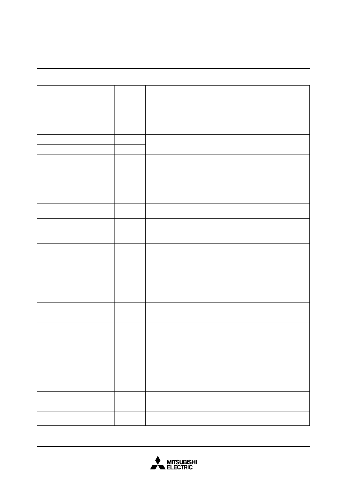
PIN DESCRIPTION
Pin
VCC, VSS
CNVSS
______
RESET
X
IN
XOUT
_
E
BYTE
CC,
AV
AV
SS
VREF
P00 – P07
P10 – P17
P20 – P27
P30 – P33
P40 – P47
P50 – P57
P60 – P67
P70 – P77
P80 – P87
Name
Power supply
CNVSS input
Reset input
Clock input
Clock output
Enable output
Bus width selection
input
Analog supply input
Reference voltage
input
I/O port P0
I/O port P1
I/O port P2
I/O port P3
I/O port P4
I/O port P5
I/O port P6
I/O port P7
I/O port P8
Input/Output
Input
Input
Input
Output
Output
Input
Input
I/O
I/O
I/O
I/O
I/O
I/O
I/O
I/O
I/O
Functions
Supply 2.7 – 5.5 V to VCC and 0 V to VSS.
This pin controls the processor mode. Connect to VSS for single-chip mode, and
CC for external ROM types.
to V
To enter the reset state, this pin must be kept at a “L” condition which should be
maintained for the required time.
These are I/O pins of internal clock generating circuit. Connect a ceramic or quartz
IN
and X
OUT
crystal resonator between X
source should be connected to the X
. When an external clock is used, the clock
IN
pin and the X
OUT
pin should be left open.
Data or instruction read and data write are performed when output from this pin
is “L”.
In memory expansion mode or microprocessor mode, this pin determines
whether the external data bus is 8-bit width or 16-bit width. The width is 16 bits
when “L” signal inputs and 8 bits when “H” signal inputs.
Power supply for the A-D converter. Connect AV
CC to VCC and AVSS to VSS
externally.
This is reference voltage input pin for the A-D converter.
In single-chip mode, port P0 becomes an 8-bit I/O port. An I/O direction register
is available so that each pin can be programmed for input or output. These ports
are in input mode when reset.
Address (A7 – A0) is output in memory expansion mode or microprocessor mode.
In single-chip mode, these pins have the same functions as port P0. When the
BYTE pin is set to “L” in memory expansion mode or microprocessor mode and
external data bus is 16-bit width, high-order data (D15 – D8) is input or output
__
when E output is “L” and an address (A15 – A8) is output when E output is “H”.
If the BYTE pin is “H” that is an external data bus is 8-bit width, only address
(A15 – A8) is output.
In single-chip mode, these pins have the same functions as port P0. In memory
expansion mode or microprocessor mode low-order data (D
output when E output is “L” and an address (A23 – A16) is output when E output
__
7 – D0) is input or
is “H”.
In single-chip mode, these pins have the same functions as port P0. In memory
expansion mode or microprocessor mode, R/W, BHE, ALE and HLDA signals
__ ____
_____
are output.
In single-chip mode, these pins have the same functions as port P0. In memory
expansion mode or microprocessor mode, P40 and P41 become HOLD and RDY
_____
____
input pin respectively. Functions of other pins are the same as in single-chip
mode. In single-chip mode or memory expansion mode, port P42 can be programmed for φ
mode. P4
1 output pin divided the clock to XIN pin by 2. In microprocessor
2 always has the function as φ1 output pin.
In addition to having the same functions as port P0 in single-chip mode, these
pins also function as I/O pins for timer A0, timer A1, timer A2 and timer A3.
In addition to having the same functions as port P0 in single-chip mode, these
pins also function as I/O pins for timer A4, external interrupt input INT0, INT1 and
____
INT2 pins, and input pins for timer B0, timer B1 and timer B2.
____ ____
In addition to having the same functions as port P0 in single-chip mode, these
pins also function as analog input AN
0 – AN7 input pins. P77 also has an A-D
conversion trigger input function.
In addition to having the same functions as port P0 in single-chip mode, these
pins also function as RXD, TXD, CLK, CTS/RTS pins for UART 0 and UART 1.
____ ____
5
MITSUBISHI MICROCOMPUTERS
M37702M2LXXXGP, M37702S1LGP
M37702M2LXXXHP, M37702S1LHP
SINGLE-CHIP 16-BIT CMOS MICROCOMPUTER
BASIC FUNCTION BLOCKS
The M37702M2LXXXGP has the same functions as the
M37702M2BXXXFP except for the reset circuit.
Refer to the section on the M37702M2BXXXFP.
RESET CIRCUIT
Reset occurs when the RESET pin is returned to “H” level after
holding it at “L” level when the power voltage is at 2.7 – 5.5 V. Program execution starts at the address formed by setting the
address pins A
FFFF
16, and A7 – A0 to the contents of address FFFE16.
(1) Port P0 data direction register
(2) Port P1 data direction register
(3) Port P2 data direction register
(4) Port P3 data direction register
(5) Port P4 data direction register
(6) Port P5 data direction register
(7) Port P6 data direction register
(8) Port P7 data direction register
(9) Port P8 data direction register
(10) A-D control register
(11)
(12)
register
(13)
register
(14)
(15)
(16)
(17)
(18) Count start flag
(19) One- shot start flag
(20) Up-down flag
(21) Timer A0 mode register
(22) Timer A1 mode register
(23) Timer A2 mode register
(24) Timer A3 mode register
(25) Timer A4 mode register
(26) Timer B0 mode register
(27) Timer B1 mode register
(28) Timer B2 mode register
23 – A16 to 0016, A15 – A8 to the contents of address
A-D sweep pin selection register
UART 0 transmit/receive mode
UART 1 transmit/receive mode
UART 0 transmit/receive
control register 0
UART 1 transmit/receive
control register 0
UART 0 transmit/receive
control register 1
UART 1 transmit/receive
control register 1
______
Address
16)•••
(04
(0516)•••
(0816)•••
(0916)•••
(0C16)•••
(0D16)•••
(1016)•••
(1116)•••
(1416)•••
(1E16)•••
(1F16)•••
(3016)•••
(3816)•••
(3416)•••
(3C16)•••
(3516)•••
(3D16)•••
(4016)•••
(4216)•••
(4416)•••
(5616)•••
(5716)•••
(5816)•••
(5916)•••
(5A16)•••
(5B16)•••
(5C16)•••
(5D16)•••
0016
00
16
0016
0000
0016
0016
0016
0016
0016
0
0000 ???
11
0016
0016
00
10
0010
0000
000010
0000
00
10
16
000 00
0016
0016
0016
0016
0016
0016
001 00 00
001
00 00
001 00 00
Figure 1 shows the status of the internal registers when a reset
occurs.
Figure 2 shows an example of a reset circuit. The reset input voltage must be held 0.55 V or lower when the power voltage reaches
2.7 V.
Address
(29) Processor mode register
(30) Watchdog timer
Watchdog timer frequency selection
flag
(32)
A-D conversion interrupt control register
(33)
UART 0 transmission interrupt control
(34)
(35)
(36)
(37)
(38)
(39)
(40)
(41)
(42)
(43)
(44)
(45)
(46)
(47)
(48) Processor status register PS
(49) Program bank register PG
(50) Program counter PC
(51) Program counter PCL
(52) Direct page register DPR
(53) Data bank register DT
Contents of other registers and RAM are not initialized and should be initialized by software.
register
UART 0 receive interrupt control register
UART 1 transmission interrupt control
register
UART 1 receive interrupt control register
Timer A0 interrupt control register
Timer A1 interrupt control register
Timer A2 interrupt control register
Timer A3 interrupt control register
Timer A4 interrupt control register
Timer B0 interrupt control register
Timer B1 interrupt control register
Timer B2 interrupt control register
INT
0
interrupt control register
INT
1
interrupt control register
INT
2
interrupt control register
H
(5E16)•••
(6016)•••
(6116)•••(31)
(7016)•••
(7116)•••
(7216)•••
(7316)•••
(7416)•••
(7516)•••
(7616)•••
(7716)•••
(7816)•••
(7916)•••
(7A16)•••
(7B16)•••
(7C16)•••
(7D16)•••
(7E16)•••
(7F16)•••
0016
FFF16
0000
0000
0000
0000
0000
0000
0000
0000
0000
0000
0000
0000
0000
000
0
0
0
000
0
0
0
0
0
000
0
?
?000
00
1??
0
0016
Content of FFFF16
Content of FFFE16
000016
0016
00
Fig. 1 Microcomputer internal status during reset
6

MITSUBISHI MICROCOMPUTERS
M37702M2LXXXGP, M37702S1LGP
M37702M2LXXXHP, M37702S1LHP
SINGLE-CHIP 16-BIT CMOS MICROCOMPUTER
ADDRESSING MODES
M37702M2LXXXGP
RESET
CC
V
V
CC
0V
6726
RESET
0V
Power on
2.7V
0.55V
Fig. 2 Example of a reset circuit (perform careful evaluation
at the system design level before using)
MEMORY
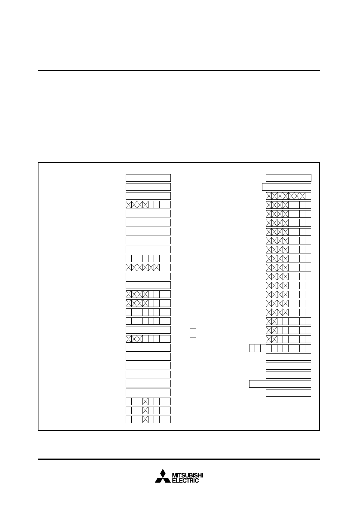
The memory map is shown in Figure 3.
The M37702M2LXXXGP has 28 powerful addressing modes.
Refer to the 7700 Family addressing mode description for the details of each addressing mode.
MACHINE INSTRUCTION LIST
The M37702M2LXXXGP has 103 machine instructions. Refer to
the 7700 Family machine instruction list for details.
DATA REQUIRED FOR MASK ORDERING
Please send the following data for mask orders.
M37702M2LXXXGP;
(1) M37702M2LXXXGP mask ROM order confirmation form
(2) 80P6S mark specification form
(3) ROM data (EPROM 3 sets)
M37702M2LXXXHP;
(1) M37702M2LXXXHP mask ROM order confirmation form
(2) 80P6D mark specification form
(3) ROM data (EPROM 3 sets)
Bank 0
16
Bank 1
16
• • • • • • • • • •
Bank FE
16
Bank FF
16
000000
00FFFF
010000
01FFFF
FE0000
FEFFFF
FF0000
FFFFFF
000000
16
00007F
000080
16
16
16
Internal RAM
16
16
00027F
512 bytes
16
000000
00007F
16
Peripheral devices
control registers
16
Interrupt vector table
00FFD6
16
A-D conversion
16
16
00C000
16
Internal ROM
16K bytes
16
16
00FFD6
16
16
00FFFF
16
00FFFE
UART1 transmission
UART1 receive
UART0 transmission
UART0 receive
Timer B2
Timer B1
Timer B0
Timer A4
Timer A3
Timer A2
Timer A1
Timer A0
INT
INT
INT
Watchdog timer
DBC
BRK instruction
Zero divide
16
RESET
2
1
0
Fig. 3 Memory map
7

MITSUBISHI MICROCOMPUTERS
M37702M2LXXXGP, M37702S1LGP
M37702M2LXXXHP, M37702S1LHP
SINGLE-CHIP 16-BIT CMOS MICROCOMPUTER
ABSOLUTE MAXIMUM RATINGS
RatingsSymbol Parameter Conditions Unit
VCC
AVCC
VI
VI
VO
Pd
Topr
Tstg
Supply voltage
Analog supply voltage
Input voltage
Input voltage P0
______
RESET, CNVSS, BYTE
0–P07, P10–P17, P20–P27, P30–P33,
P4
0–P47, P50–P57, P60–P67, P70–P77,
0–P87, VREF, XIN
P8
Output voltage P00–P07, P10–P17, P20–P27, P30–P33,
0–P47, P50–P57, P60–P67, P70–P77,
P4
P80–P87, XOUT, E
_
Power dissipation
Operating temperature
Storage temperature
a = 25 °C
T
–0.3 to 7
–0.3 to 7
–0.3 to 12
–0.3 to V
–0.3 to V
300 (Note 1)
–40 to 85
–65 to 150
CC+0.3
CC+0.3
Note 1. In the case of M37702M2LXXXHP and M37702S1LHP, the rating of power dissipation is 200 mW.
RECOMMENDED OPERATING CONDITIONS (VCC = 2.7 to 5.5 V, Ta = –40 to 85 °C, unless otherwise noted)
CC
Limits
Typ.
CC
V
0
0
Max.
5.5
CC
V
VCC
VCC
0.2VCC
0.2VCC
0.16VCC
–10
–5
10
5
8
Symbol Parameter Unit
VCC
AVCC
VSS
AVSS
VIH
VIH
Supply voltage
Analog supply voltage
Supply voltage
Analog supply voltage
High-level input voltage P0
P60–P67, P70–P77, P80–P87, XIN, RESET,
CNV
High-level input voltage P1
0–P07, P30–P33, P40–P47, P50–P57,
SS, BYTE
0–P17, P20–P27
______
Min.
2.7
0.8V
0.8VCC
(in single-chip mode)
VIH
High-level input voltage P1
0–P17, P20–P27
0.5VCC
(in memory expansion mode and microprocessor mode)
VIL
VIL
Low-level input voltage P0
Low-level input voltage P1
0–P07, P30–P33, P40–P47, P50–P57,
P60–P67, P70–P77, P80–P87, XIN, RESET,
CNV
SS, BYTE
0–P17, P20–P27
______
0
0
(in single-chip mode)
VIL
Low-level input voltage P1
0–P17, P20–P27
0
(in memory expansion mode and microprocessor mode)
IOH(peak)
IOH(avg)
IOL(peak)
IOL(avg)
f(XIN)
High-level peak output current P0
High-level average output current P00–P07, P10–P17, P20–P27, P30–P33,
Low-level peak output current P00–P07, P10–P17, P20–P27, P30–P33,
Low-level average output current P00–P07, P10–P17, P20–P27, P30–P33,
External clock frequency input
0–P07, P10–P17, P20–P27, P30–P33,
0–P47, P50–P57, P60–P67, P70–P77,
P4
P8
0–P87
P4
0–P47, P50–P57, P60–P67, P70–P77,
0–P87
P8
P4
0–P47, P50–P57, P60–P67, P70–P77,
0–P87
P8
P4
0–P47, P50–P57, P60–P67, P70–P77,
0–P87
P8
Note 2. Average output current is the average value of a 100 ms interval.
3. The sum of I
must be 80 mA or less, the sum of I
OL(peak) for ports P0, P1, P2, P3, and P8 must be 80 mA or less, the sum of IOH(peak) for ports P0, P1, P2, P3, and P8
OL(peak) for ports P4, P5, P6, and P7 must be 80 mA or less, and the sum of IOH(peak) for ports
P4, P5, P6, and P7 must be 80 mA or less.
V
V
V
V
V
mW
°C
°C
V
V
V
V
V
V
V
V
V
V
mA
mA
mA
mA
MHz
8

MITSUBISHI MICROCOMPUTERS
M37702M2LXXXGP, M37702S1LGP
M37702M2LXXXHP, M37702S1LHP
SINGLE-CHIP 16-BIT CMOS MICROCOMPUTER
ELECTRICAL CHARACTERISTICS (VCC = 5 V, VSS = 0 V, Ta = 25 °C, f(XIN) = 8 MHz, unless otherwise noted)
Symbol Parameter Test conditions Unit
VOH
VOH
VOH
High-level output voltage P00–P07, P10–P17, P20–P27,
0
, P31, P33, P40–P47, P50–P57,
P3
P6
0
–P67, P70–P77, P80–P8
7
High-level output voltage P00–P07, P10–P17, P20–P27,
0
, P31, P3
P3
High-level output voltage P3
2
3
VCC = 5 V, IOH = –10 mA
VCC = 3 V, IOH = –1 mA
VCC = 5 V, IOH = –400 µA
V
CC = 5 V, IOH = –10 mA
VCC = 5 V, IOH = –400 µA
VCC = 3 V, IOH = –1 mA
VOH
High-level output voltage_E
VCC = 5 V, IOH = –10 mA
VCC = 5 V, IOH = –400 µA
VCC = 3 V, IOH = –1 mA
VOL
VOL
VOL
Low-level output voltage P00–P07, P10–P17, P20–P27,
P3
0
, P31, P33, P40–P47, P50–P57,
0
–P67, P70–P77, P80–P8
P6
7
Low-level output voltage P00–P07, P10–P17, P20–P27,
P3
0
, P31, P3
3
Low-level output voltage P3
2
CC = 5 V, IOL = 10 mA
V
VCC = 3 V, IOL = 1 mA
V
CC = 5 V, IOL = 2 mA
CC = 5 V, IOL = 10 mA
V
VCC = 5 V, IOL = 2 mA
VCC = 3 V, IOL = 1 mA
VOL
Low-level output voltage_E
VCC = 5 V, IOL = 10 mA
VCC = 5 V, IOL = 2 mA
VCC = 3 V, IOL = 1 mA
VCC = 5 V
1
VCC = 3 V
VCC = 5 V
VT+ – VT–
VT+ – VT–
Hysteresis
Hysteresis
_____
____
HOLD, RDY, TA0IN–TA4IN, TB0IN–TB2IN,
____ ____
INT0–INT2, AD
______
RESET
_____ ____ ____ ____ ____
TRG
, CTS0, CTS1, CLK0, CLK
VCC = 3 V
VT+ – VT–
Hysteresis X
IN
VCC = 5 V
VCC = 3 V
IIH
IIL
VRAM
ICC
High-level input current P00–P07, P10–P17, P20–P27,
0
–P33, P40–P47, P50–P57,
P3
P6
0
–P67, P70–P77, P80–P8
______
XIN, RESET, CNVSS, BYTE
Low-level input current P00–P07, P10–P17, P20–P27,
P3
0
–P33, P40–P47, P50–P57,
0
–P67, P70–P77, P80–P8
P6
______
XIN, RESET, CNVSS, BYTE
RAM hold voltage
Power supply current
V
CC = 5 V, VI = 5 V
7,
VCC = 3 V, VI = 3 V
V
CC = 5 V, VI = 0 V
7,
VCC = 3 V, VI = 0 V
When clock is stopped.
In singlechip mode
output only
pin is open
and other
pins are V
during reset.
f(XIN) = 8 MHz,
square waveform
Ta = 25 °C when clock
is stopped.
SS
T
is stopped.
VCC = 5 V
VCC = 3 V
a = 85 °C when clock
Limits
Min. Typ. Max.
3
2.5
4.7
3.1
4.8
2.6
3.4
4.8
2.6
0.5
0.45
1.9
0.43
0.4
1.6
0.4
0.4
0.4
0.1
0.2
0.1
0.1
0.06
0.7
0.5
0.4
0.3
0.2
–5
–4
2
6
12
4
20
V
V
V
V
2
V
V
V
V
1
V
V
V
5
µA
4
µA
V
mA
8
1
µA
A-D CONVERTER CHARACTERISTICS (VCC = 5 V, VSS = 0 V, Ta = 25 °C, f(XIN) = 8 MHz, unless otherwise noted)
Symbol Parameter Test conditions Unit
LADDER
R
tCONV
VREF
VIA
—
—
Resolution
Absolute accuracy
Ladder resistance
Conversion time
Reference voltage
Analog input voltage
REF = VCC
V
VREF = VCC
VREF = VCC
Min. Typ. Max.
28.5
2.7
Limits
8
±3
2
0
10
CC
V
VREF
Bits
LSB
kΩ
µs
V
V
9

MITSUBISHI MICROCOMPUTERS
M37702M2LXXXGP, M37702S1LGP
M37702M2LXXXHP, M37702S1LHP
SINGLE-CHIP 16-BIT CMOS MICROCOMPUTER
TIMING REQUIREMENTS (VCC = 2.7 to 5.5 V, VSS = 0 V, Ta = 25 °C, f(XIN) = 8 MHz, unless otherwise noted) External clock input
Symbol Parameter Unit
tC
tW(H)
tW(L)
tr
tf
External clock input cycle time
External clock input high-level pulse width
External clock input low-level pulse width
External clock rise time
External clock fall time
Single-chip mode
Symbol Parameter Unit
tsu(P0D–E)
tsu(P1D–E)
tsu(P2D–E)
tsu(P3D–E)
tsu(P4D–E)
tsu(P5D–E)
tsu(P6D–E)
tsu(P7D–E)
tsu(P8D–E)
th(E–P0D)
th(E–P1D)
th(E–P2D)
th(E–P3D)
th(E–P4D)
th(E–P5D)
th(E–P6D)
th(E–P7D)
th(E–P8D)
Port P0 input setup time
Port P1 input setup time
Port P2 input setup time
Port P3 input setup time
Port P4 input setup time
Port P5 input setup time
Port P6 input setup time
Port P7 input setup time
Port P8 input setup time
Port P0 input hold time
Port P1 input hold time
Port P2 input hold time
Port P3 input hold time
Port P4 input hold time
Port P5 input hold time
Port P6 input hold time
Port P7 input hold time
Port P8 input hold time
Min.
125
50
50
Min.
300
300
300
300
300
300
300
300
300
Limits
Limits
0
0
0
0
0
0
0
0
0
Max.
20
20
Max.
ns
ns
ns
ns
ns
ns
ns
ns
ns
ns
ns
ns
ns
ns
ns
ns
ns
ns
ns
ns
ns
ns
ns
Memory expansion mode and microprocessor mode
Symbol Parameter Unit
tsu(P1D–E)
tsu(P2D–E)
tsu(RDY–φ1)
tsu
(HOLD–φ1)
th(E–P1D)
th(E–P2D)
th(φ1–RDY)
th(φ1–HOLD)
10
Port P1 input setup time
Port P2 input setup time
____
RDY input setup time
_____
HOLD input setup time
Port P1 input hold time
Port P2 input hold time
____
RDY input hold time
_____
HOLD input hold time
Min.
80
80
90
90
0
0
0
0
Limits
Max.
ns
ns
ns
ns
ns
ns
ns
ns

MITSUBISHI MICROCOMPUTERS
M37702M2LXXXGP, M37702S1LGP
M37702M2LXXXHP, M37702S1LHP
SINGLE-CHIP 16-BIT CMOS MICROCOMPUTER
Timer A input (Count input in event counter mode)
Symbol Parameter Unit
tC(TA)
tW(TAH)
tW(TAL)
TAiIN input cycle time
IN input high-level pulse width
TAi
IN input low-level pulse width
TAi
Timer A input (Gating input in timer mode)
Symbol Parameter Unit
tC(TA)
tW(TAH)
tW(TAL)
TAiIN input cycle time
IN input high-level pulse width
TAi
IN input low-level pulse width
TAi
Min.
250
125
125
Min.
1000
500
500
Limits
Max.
ns
ns
ns
Limits
Max.
ns
ns
ns
Timer A input (External trigger input in one-shot pulse mode)
Symbol Parameter Unit
tC(TA)
tW(TAH)
tW(TAL)
TAiIN input cycle time
IN input high-level pulse width
TAi
IN input low-level pulse width
TAi
Min.
500
250
250
Limits
Max.
Timer A input (External trigger input in pulse width modulation mode)
Symbol Parameter Unit
tW(TAH)
tW(TAL)
TAiIN input high-level pulse width
IN input low-level pulse width
TAi
Min.
250
250
Limits
Max.
Timer A input (Up-down input in event counter mode)
Symbol Parameter Unit
tC(UP)
tW(UPH)
tW(UPL)
tsu(UP-TIN)
th(TIN-UP)
TAiOUT input cycle time
OUT input high-level pulse width
TAi
OUT input low-level pulse width
TAi
OUT input setup time
TAi
OUT input hold time
TAi
Min.
5000
2500
2500
1000
1000
Limits
Max.
ns
ns
ns
ns
ns
ns
ns
ns
ns
ns
11

MITSUBISHI MICROCOMPUTERS
M37702M2LXXXGP, M37702S1LGP
M37702M2LXXXHP, M37702S1LHP
SINGLE-CHIP 16-BIT CMOS MICROCOMPUTER
Timer B input (Count input in event counter mode)
Symbol Parameter Unit
tC(TB)
tW(TBH)
tW(TBL)
tC(TB)
tW(TBH)
tW(TBL)
TBiIN input cycle time (one edge count)
IN input high-level pulse width (one edge count)
TBi
IN input low-level pulse width (one edge count)
TBi
IN input cycle time (both edges count)
TBi
IN input high-level pulse width (both edges count)
TBi
IN input low-level pulse width (both edges count)
TBi
Timer B input (Pulse period measurement mode)
Symbol Parameter Unit
tC(TB)
tW(TBH)
tW(TBL)
TBiIN input cycle time
IN input high-level pulse width
TBi
IN input low-level pulse width
TBi
Min.
250
125
125
500
250
250
Min.
1000
500
500
Limits
Max.
ns
ns
ns
ns
ns
ns
Limits
Max.
ns
ns
ns
Timer B input (Pulse width measurement mode)
Symbol Parameter Unit
tC(TB)
tW(TBH)
tW(TBL)
TBiIN input cycle time
IN input high-level pulse width
TBi
IN input low-level pulse width
TBi
Min.
1000
500
500
Limits
Max.
A-D trigger input
Symbol Parameter Unit
tC(AD)
tW(ADL)
______
ADTRG input cycle time (minimum allowable trigger)
_____
ADTRG input low-level pulse width
Min.
2000
250
Limits
Max.
Serial I/O
Symbol Parameter Unit
tC(CK)
tW(CKH)
tW(CKL)
td(C–Q)
th(C–Q)
tsu(D–C)
th(C–D)
CLKi input cycle time
i input high-level pulse width
CLK
i input low-level pulse width
CLK
i output delay time
TxD
i hold time
TxD
i input setup time
RxD
i input hold time
RxD
Min.
500
250
250
0
80
100
Limits
Max.
170
ns
ns
ns
ns
ns
ns
ns
ns
ns
ns
ns
ns
External interrupt INTi input
_____
Symbol Parameter
tW(INH)
tW(INL)
12
____
INTi input high-level pulse width
____
INTi input low-level pulse width
Min.
250
250
Limits
Unit
Max.
ns
ns

MITSUBISHI MICROCOMPUTERS
M37702M2LXXXGP, M37702S1LGP
M37702M2LXXXHP, M37702S1LHP
SINGLE-CHIP 16-BIT CMOS MICROCOMPUTER
SWITCHING CHARACTERISTICS (VCC = 2.7 to 5.5 V, VSS = 0 V, Ta = 25 °C, f(XIN) = 8 MHz, unless otherwise noted) Single-chip mode
Symbol Parameter Unit
td(E–P0Q)
td(E–P1Q)
td(E–P2Q)
td(E–P3Q)
td(E–P4Q)
td(E–P5Q)
td(E–P6Q)
td(E–P7Q)
td(E–P8Q)
Port P0 data output delay time
Port P1 data output delay time
Port P2 data output delay time
Port P3 data output delay time
Port P4 data output delay time
Port P5 data output delay time
Port P6 data output delay time
Port P7 data output delay time
Port P8 data output delay time
Test conditions
Fig. 4
Limits
Min. Max.
300
300
300
300
300
300
300
300
300
ns
ns
ns
ns
ns
ns
ns
ns
ns
Memory expansion mode and microprocessor mode (when wait bit = “0”, and external memory area is accessed)
Symbol Parameter Unit
td(P0A–E)
td(E–P1Q)
tPXZ(E–P1Z)
td(P1A–E)
td(P1A–ALE)
td(E–P2Q)
tPXZ(E–P2Z)
td(P2A–E)
td(P2A–ALE)
td(φ1–HLDA)
td(ALE–E)
tW(ALE)
td(BHE–E)
td(R/W–E)
td(E–φ1)
th(E–P0A)
th(ALE–P1A)
th(E–P1Q)
tPZX(E–P1Z)
th(E–P1A)
th(ALE–P2A)
th(E–P2Q)
tPZX(E–P2Z)
th(E–BHE)
th(E–R/W)
tW(EL)
Port P0 address output delay time
Port P1 data output delay time (BYTE = “L”)
Port P1 floating start delay time (BYTE = “L”)
Port P1 address output delay time
Port P1 address output delay time
Port P2 data output delay time
Port P2 floating start delay time
Port P2 address output delay time
Port P2 address output delay time
_____
HLDA output delay time
ALE output delay time
ALE pulse width
____
BHE output delay time
__
R/W output delay time
1 output delay time
φ
Port P0 address hold time
Port P1 address hold time (BYTE = “L”)
Port P1 data hold time (BYTE = “L”)
Port P1 floating release delay time (BYTE = “L”)
Port P1 address hold time (BYTE = “H”)
Port P2 address hold time
Port P2 data hold time
Port P2 floating release delay time
____
BHE hold time
__
R/W hold time
_
E pulse width
Test conditions
Fig. 4
Min.
50
50
40
50
40
60
50
50
50
50
95
50
50
95
18
18
460
Limits
4
0
9
9
Max.
130
10
130
10
120
40
ns
ns
ns
ns
ns
ns
ns
ns
ns
ns
ns
ns
ns
ns
ns
ns
ns
ns
ns
ns
ns
ns
ns
ns
ns
ns
13

MITSUBISHI MICROCOMPUTERS
M37702M2LXXXGP, M37702S1LGP
M37702M2LXXXHP, M37702S1LHP
SINGLE-CHIP 16-BIT CMOS MICROCOMPUTER
Memory expansion mode and microprocessor mode (when wait bit = “1”)
Symbol Parameter Unit
td(P0A–E)
td(E–P1Q)
tPXZ(E–P1Z)
td(P1A–E)
td(P1A–ALE)
td(E–P2Q)
tPXZ(E–P2Z)
td(P2A–E)
td(P2A–ALE)
td(φ1–HLDA)
td(ALE–E)
tW(ALE)
td(BHE–E)
td(R/W–E)
td(E–φ1)
th(E–P0A)
th(ALE–P1A)
th(E–P1Q)
tPZX(E–P1Z)
th(E–P1A)
th(ALE–P2A)
th(E–P2Q)
tPZX(E–P2Z)
th(E–BHE)
th(E–R/W)
tW(EL)
Port P0 address output delay time
Port P1 data output delay time (BYTE = “L”)
Port P1 floating start delay time (BYTE = “L”)
Port P1 address output delay time
Port P1 address output delay time
Port P2 data output delay time
Port P2 floating start delay time
Port P2 address output delay time
Port P2 address output delay time
_____
HLDA output delay time
ALE output delay time
ALE pulse width
____
BHE output delay time
__
R/W output delay time
1 output delay time
φ
Port P0 address hold time
Port P1 address hold time (BYTE = “L”)
Port P1 data hold time (BYTE = “L”)
Port P1 floating release delay time (BYTE = “L”)
Port P1 address hold time (BYTE = “H”)
Port P2 address hold time
Port P2 data hold time
Port P2 floating release delay time
____
BHE hold time
__
R/W hold time
_
E pulse width
Test conditions
Fig. 4
Min.
50
50
40
50
40
60
50
50
50
50
95
50
50
95
18
18
210
Limits
4
0
9
9
Max.
130
10
130
10
120
40
ns
ns
ns
ns
ns
ns
ns
ns
ns
ns
ns
ns
ns
ns
ns
ns
ns
ns
ns
ns
ns
ns
ns
ns
ns
ns
14
P 0
P 1
P 2
P 3
P 4
P 5
P 6
P 7
P 8
φ
1
E
Fig. 4 Testing circuit for ports P0–P8, φ1
100 pF

MITSUBISHI MICROCOMPUTERS
M37702M2LXXXGP, M37702S1LGP
M37702M2LXXXHP, M37702S1LHP
SINGLE-CHIP 16-BIT CMOS MICROCOMPUTER
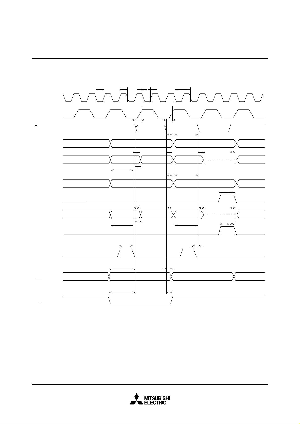
TIMING DIAGRAM
Single-chip mode
f(XIN)
E
Port P0 output
Port P0 input
Port P1 output
Port P1 input
Port P2 output
Port P2 input
Port P3 output
Port P3 input
Port P4 output
Port P4 input
trt
f
t
c
tsu(P0D–E) th(E–P0D)
tsu(P1D–E) th(E–P1D)
tsu(P2D–E)
tsu(P3D–E) th(E–P3D)
tsu(P4D–E)
td(E–P0Q)
td(E–P1Q)
td(E–P2Q)
th(E–P2D)
td(E–P3Q)
td(E–P4Q)
th(E–P4D)
t
w(H)
t
w(L)
Port P5 output
Port P5 input
Port P6 output
Port P6 input
Port P7 output
Port P7 input
Port P8 output
Port P8 input
td(E–P5Q)
tsu(P5D–E)
th(E–P5D)
td(E–P6Q)
tsu(P6D–E) th(E–P6D)
td(E–P7Q)
tsu(P7D–E) th(E–P7D)
td(E–P8Q)
tsu(P8D–E)
th(E–P8D)
15

MITSUBISHI MICROCOMPUTERS
M37702M2LXXXGP, M37702S1LGP
M37702M2LXXXHP, M37702S1LHP
SINGLE-CHIP 16-BIT CMOS MICROCOMPUTER
t
c(TA)
t
w(TAH)
TAiIN input
t
w(TAL)
t
c(UP)
t
w(UPH)
TAi
OUT
input
t
w(UPL)
In Event counter mode
TBiIN input
AD
TRG
input
CLK
i
TAi
OUT
input
(Up-down input)
TAi
IN
input
(when count by falling)
TAi
IN
input
(when count by rising)
t
w(TBH)
t
w(ADL)
t
w(CKH)
t
h(TIN–UP)tsu(UP–TIN)
t
c(TB)
t
w(TBL)
t
c(AD)
t
c(CK)
t
w(CKL)
t
h(C–Q)
TxD
RxD
INTi
16
i
i
input
t
w(INL)
t
d(C–Q)
t
w(INH)
t
su(D–C)
t
h(C–D)

MITSUBISHI MICROCOMPUTERS
M37702M2LXXXGP, M37702S1LGP
M37702M2LXXXHP, M37702S1LHP
SINGLE-CHIP 16-BIT CMOS MICROCOMPUTER
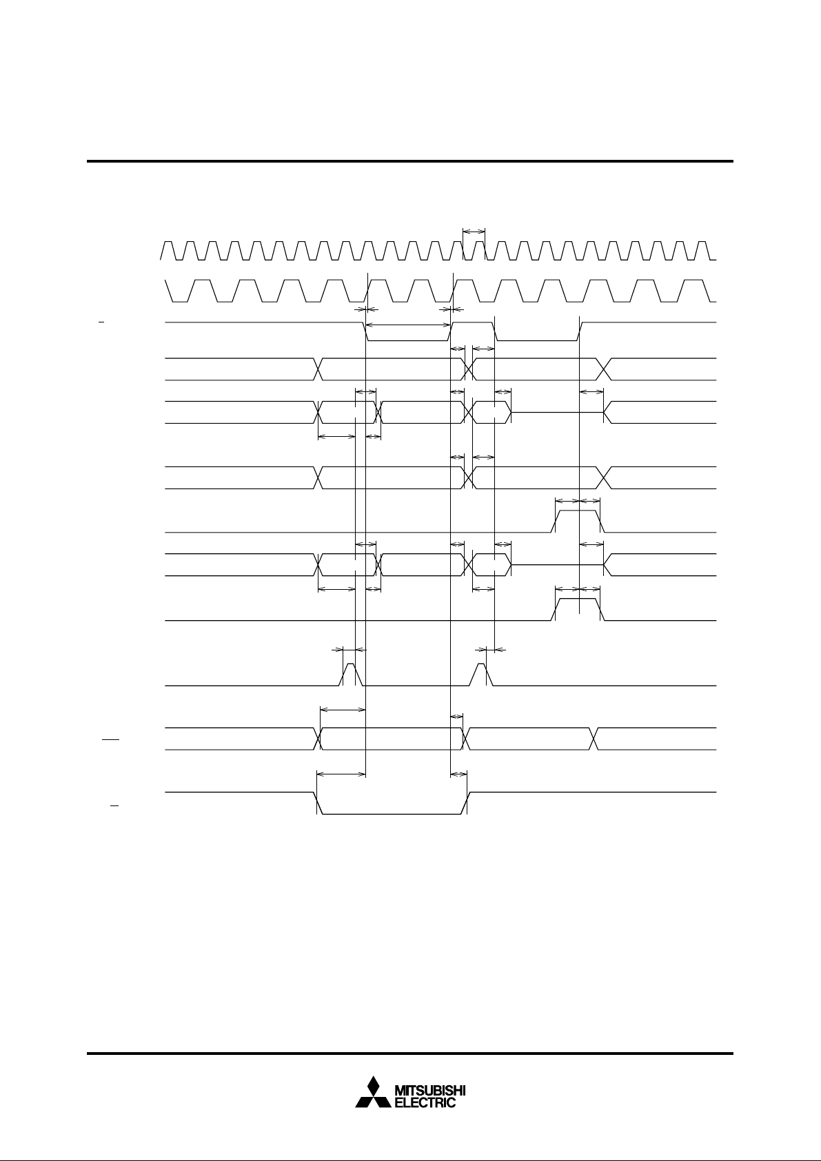
Memory expansion mode and microprocessor mode
(When wait bit = “1”)
φ
1
E
RDY
input
( When wait bit = “0”)
φ
1
E
RDY
input
(When wait bit = “1” or “0” in common)
φ
1
t
su(HOLD–
φ
1
)
HOLD
input
t
su(RDY–
t
su(RDY–
φ
1
)th(
φ
1
–RDY)
φ
1
)th(
φ
1
–RDY)
th(φ
1
–HOLD)
HLDA
output
td(φ
Test conditions
CC
= 2.7 to 5.5 V
• V
• Input timing voltage : V
• Output timing voltage : V
1
–HLDA)
IL
= 0.2 VCC, VIH = 0.8 V
OL =
0.8 V, VOH = 2.0 V
CC
td(φ
1
–HLDA)
17
MITSUBISHI MICROCOMPUTERS
M37702M2LXXXGP, M37702S1LGP
M37702M2LXXXHP, M37702S1LHP
SINGLE-CHIP 16-BIT CMOS MICROCOMPUTER
Memory expansion mode and microprocessor mode (When wait bit = “1”)
t
tw(EL)
td(E-P1Q)
td(E-P2Q)
rtf tc
th(E-P0A)
th(E-P1Q)
th(E-P1A)
d(E- φ1)td(E- φ1)
t
td(P0A-E)
AddressAddress
tpxz(E-P1Z)
Address Address
td(P1A-E)
tsu(P1D-E) th(E-P1D)
th(E-P2Q)
td(P2A-E)
tpxz(E-P2Z)
tsu(P2D-E)
tpzx(E-P1Z)
tpzx(E-P2Z)
th(E-P2D)
f(XIN)
φ1
E
Port P0 output
(A
0 to A7)
Port P1 output
(A
8 to A15/D8 to D15)
(BYTE = “L”)
Port P1 output
(A
8 to A15)
(BYTE = “H”)
Port P1 input
Port P2 output
16 to A23/D0 to D7)
(A
Port P2 input
tw(H)tw(L)
th(ALE-P1A)
Address Data
td(P1A-ALE)
Address Address
th(ALE-P2A)
Address Data Address Address
td(P2A-ALE)
2 output
Port P3
(ALE)
Port P3
1 output
(BHE)
Port P30 output
(R/W)
tw(ALE)
td(BHE-E)
td(R/W-E)
Test conditions
• V
CC = 2.7 to 5.5 V
• Output timing voltage : V
• Ports P1, P2 input : VIL = 0.16 VCC, VIH = 0.5 VCC
OL = 0.8 V, VOH = 2.0 V
td(ALE-E)
th(E-BHE)
th(E-R/W)
18
MITSUBISHI MICROCOMPUTERS
M37702M2LXXXGP, M37702S1LGP
M37702M2LXXXHP, M37702S1LHP
SINGLE-CHIP 16-BIT CMOS MICROCOMPUTER
Memory expansion mode and microprocessor mode (When wait bit = “0”, and external memory area is accessed)
c
t
f(XIN)
φ1
t
d(E- φ1)td(E- φ1)
td(P0A-E)
AddressAddress
tpxz(E-P1Z)
Address Address
td(P1A-E)
tsu(P1D-E) th(E-P1D)
tpxz(E-P2Z)
td(P2A-E)
tsu(P2D-E)
tpzx(E-P1Z)
tpzx(E-P2Z)
th(E-P2D)td(E-P2Q)
E
Port P0 output
0 to A7)
(A
Port P1 output
(A
8 to A15/D8 to D15)
(BYTE = “L”)
Port P1 output
(A
8 to A15)
(BYTE = “H”)
Port P1 input
Port P2 output
16 to A23/D0 to D7)
(A
Port P2 input
tw(EL)
th(E-P0A)
th(ALE-P1A)
Address Data
td(P1A-ALE)
Address Data Address Address
td(P2A-ALE)
th(E-P1Q)
td(E-P1Q)
th(E-P1A)
Address Address
th(E-P2Q)th(ALE-P2A)
2 output
Port P3
(ALE)
1 output
Port P3
(BHE)
Port P30 output
(R/W)
Test conditions
• V
CC = 2.7 to 5.5 V
• Output timing voltage : V
• Ports P1, P2 input : V
tw(ALE)
td(BHE-E)
td(R/W-E)
OL = 0.8 V, VOH = 2.0 V
IL = 0.16 VCC, VIH = 0.5 VCC
td(ALE-E)
th(E-BHE)
th(E-R/W)
19

MITSUBISHI DATA BOOK
SINGLE-CHIP 16-BIT MICROCOMPUTERS Vol.1
Mar. First Edition 1996
Editioned by
Committee of editing of Mitsubishi Semiconductor Data Book
Published by
Mitsubishi Electric Corp., Semiconductor Division
This book, or parts thereof, may not be reproduced in any form without permission of
Mitsubishi Electric Corporation.
©1996 MITSUBISHI ELECTRIC CORPORATION Printed in Japan
 Loading...