

Mitsubishi M37630E4FS, M37630E4FP, M37630M4T-XXXFS, M37630M4T-XXXFP, M37630E4T-XXXFP Datasheet
DESCRIPTION
g
g
g
g
guag
g
g
g
g
g
g
g
g
The 7630 group is a single chip 8-bit microcomputer designed with
CMOS silicon
equipped with a CAN (Controller Area Network) module cir-
Bein
cuit, the microcomputer is suited to drive automotive equipments.
The CAN module complies with CAN specification version 2.0, part
B and allows priority-based messa
In addition to the microcomputers simple instruction set, the ROM,
RAM and I/O addresses are placed in the same memory map to
enable easy pro
The built-in ROM is available as mask ROM or One Time PROM.
For development purposes, emulator- and EPROM-type microcomputers are available as well.
ate technology.
e management.
ramming.
FEATURES
z
Basic machine-lan
z
Minimum instruction execution time
(at 10 MHz oscillation frequency) . . . . . . . . . . . . . . . . . .0.2 µs
z
Memory size
ROM . . . . . . . . . . . . . . . . .16252 bytes (M37630M4T-XX XFP)
RAM . . . . . . . . . . . . . . . . . . .512 bytes (M37630M4T-XXXFP)
z
I/O ports
rammable I/O ports . . . . . . . . . . . . . . . . . . . . . . . . . . . .35
Pro
Input . . . . . . . . . . . . . . . . . . . . . . . . . . . . . . . . . . . . . . . . . . . .1
e instructions . . . . . . . . . . . . . . . . . .71
MITSUBISHI MICROCOMPUTERS
7630 Group
SINGLE-CHIP 8-BIT CMOS MICROCOMPUTER
z
Interrupts . . . . . . . . . . . . . . . . . . . . . . . .24 sources, 24 vectors
z
Timers
16-bit Timers . . . . . . . . . . . . . . . . . . . . . . . . . . . . . . 2 channels
8-bit Timers . . . . . . . . . . . . . . . . . . . . . . . . . . . . . . . 3 channels
z
Serial I/Os
Clock synchronous. . . . . . . . . . . . . . . . . . . . . . . . . . . 1 channel
UART . . . . . . . . . . . . . . . . . . . . . . . . . . . . . . . . . . . . . 1 channel
z
CAN module
(CAN specification version 2.0, part B) . . . . . . . . . . .1 channel
z
A-D converter. . . . . . . . . . . . . . . . . . . . . . . . 8-bits x 8 channels
z
Watchdo
z
Clock Generatin
Built-in with internal feedback resistor
z
Power source volta
(at 10 MHz oscillation frequency). . . . . . . . . . . . . . . 4.0 to 5.5 V
z
Power dissipation
In hi
(at 8 MHz oscillation frequency, at 5 V power source volta
z
Operatin
z
Packa
APPLICATION
Automotive controls
timer . . . . . . . . . . . . . . . . . . . . . . . . . . . . . . . . . . . . 1
Circuit . . . . . . . . . . . . . . . . . . . . . . . . . . . . . 1
e
h-speed mode . . . . . . . . . . . . . . . . . . . . . . . . . . . . 55 mW
temperature range. . . . . . . . . . . . . . . . . –40 to 85 °C
e. . . . . . . . . . . . . . . . . . . . . . . . . . . . 44QFP (44P6N-A)
e)
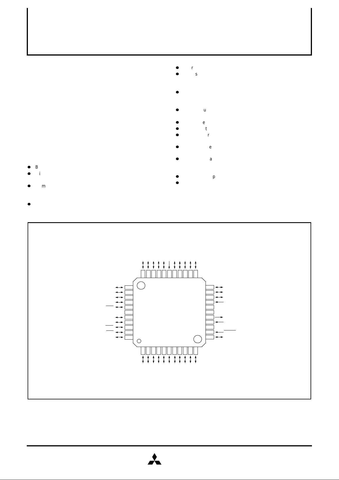
PIN CONFIGURATION (TOP VIEW)
P1
P20/S
P21/S
OUT
P22/S
CLK
P23/S
RDY
V
P24/URXD
P25/UTXD
P26/U
RTS
P27/U
CTS
P3
SS
34
7
35
IN
36
37
38
39
40
41
42
43
44
0
1
0
1
0
7
6
5
0
/CNTR
/CNTR
/INT
/TX
/PWM
5
6
P1
P1
3332313029282726252423
/INT
4
3
2
1
P1
P1
P1
P1
4
/AN
/AN
/AN
/AN
7
6
5
4
P0
P0
P0
P0
M37630M4T-XXXFP
M37630E4T-XXXFP
123456789
4
0
1
3
P3
P3
/CTX
1
P3
/CRX
2
P3
/KW
/KW
0
1
P4
P4
10
2
3
4
5
/KW
/KW
/KW
/KW
2
3
4
5
P4
P4
P4
P4
Package type: 44P6N-A
44-pin plastic molded QFP
3
/AN
3
P0
22
P02/AN
P01/AN
P00/AN
V
REF
AV
SS
V
CC
X
OUT
X
IN
V
SS
RESET
P47/KW
2
1
0
7
21
20
19
18
17
16
15
14
13
12
11
6
/KW
6
P4
Fig. 1 Pin configuration of M37630M4T–XXXFP
MITSUBISHI
ELECTRIC
1
2
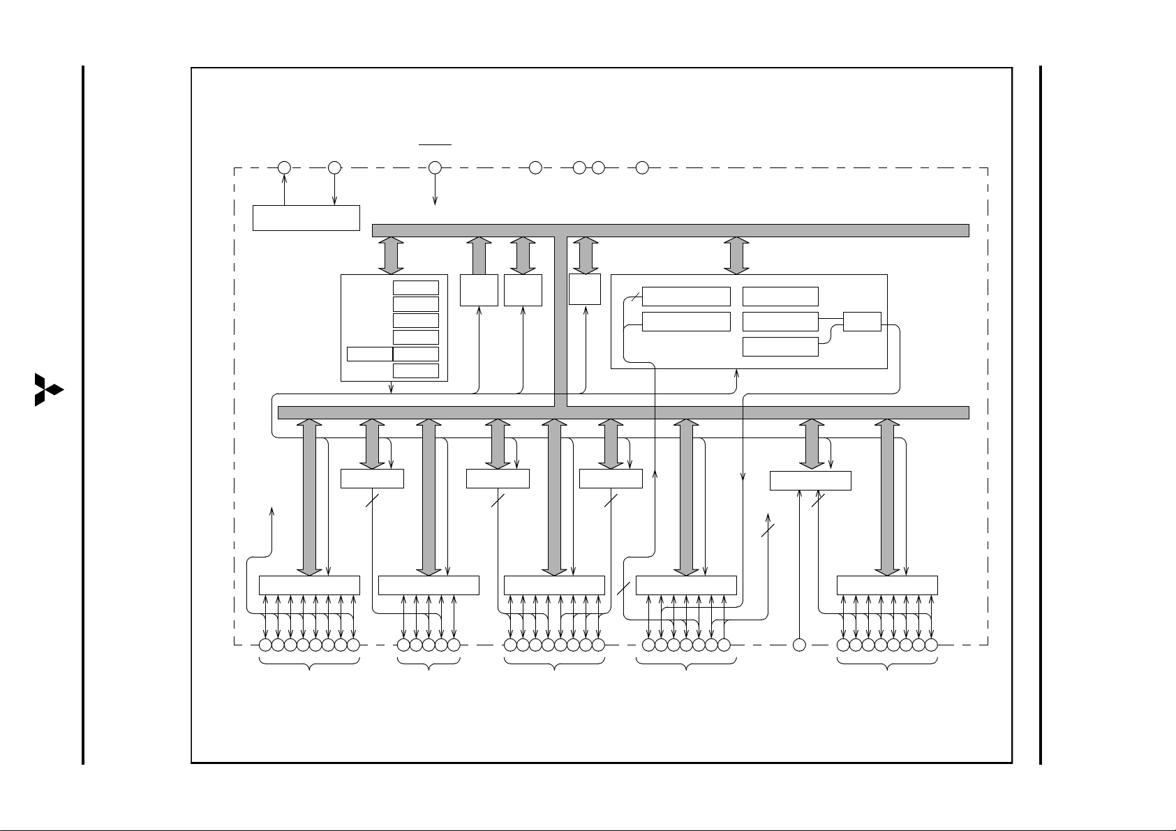
Fig. 2 Functional block diagram
M37630MXT-XXXFP FUNCTIONAL BLOCK DIAGRAM (PACKAGE: 44P6N-A)
Clock
output
X
OUT
Clock generating circuit
MITSUBISHI
ELECTRIC
key on
wake up
Clock
input
X
IN
1516 13 17 14 39 18
CPU
PCH (8)
2
RESET
A (8)
X (8)
Y (8)
S (8)
PCL (8)
PS (8)
Reset
input
UART
4
V
CC
RAMROM
V
WDT
SS
Serial I/OCAN
4
AV
SS
Time r X (16)
2
Time r Y (16)
Timer 1 (8)
Timer 2 (8)
Timer 3 (8)
A-D Converter
INT0, INT
PWM
SINGLE-CHIP 8-BIT CMOS MICROCOMPUTER
8
1
12
P4 (8)
1011
I/O port P4
2
MITSUBISHI MICROCOMPUTERS
P3 (5)
56789
441234
P2 (8)
43
35363738404142
P1 (7)
3
28293031323334
19
V
input
REF
P0 (8)
I/O port P0I/O port P1I/O port P2I/O port P3
2021222324252627
7630 Group
SINGLE-CHIP 8-BIT CMOS MICROCOMPUTER
g
g
g
g
g
g
g
g
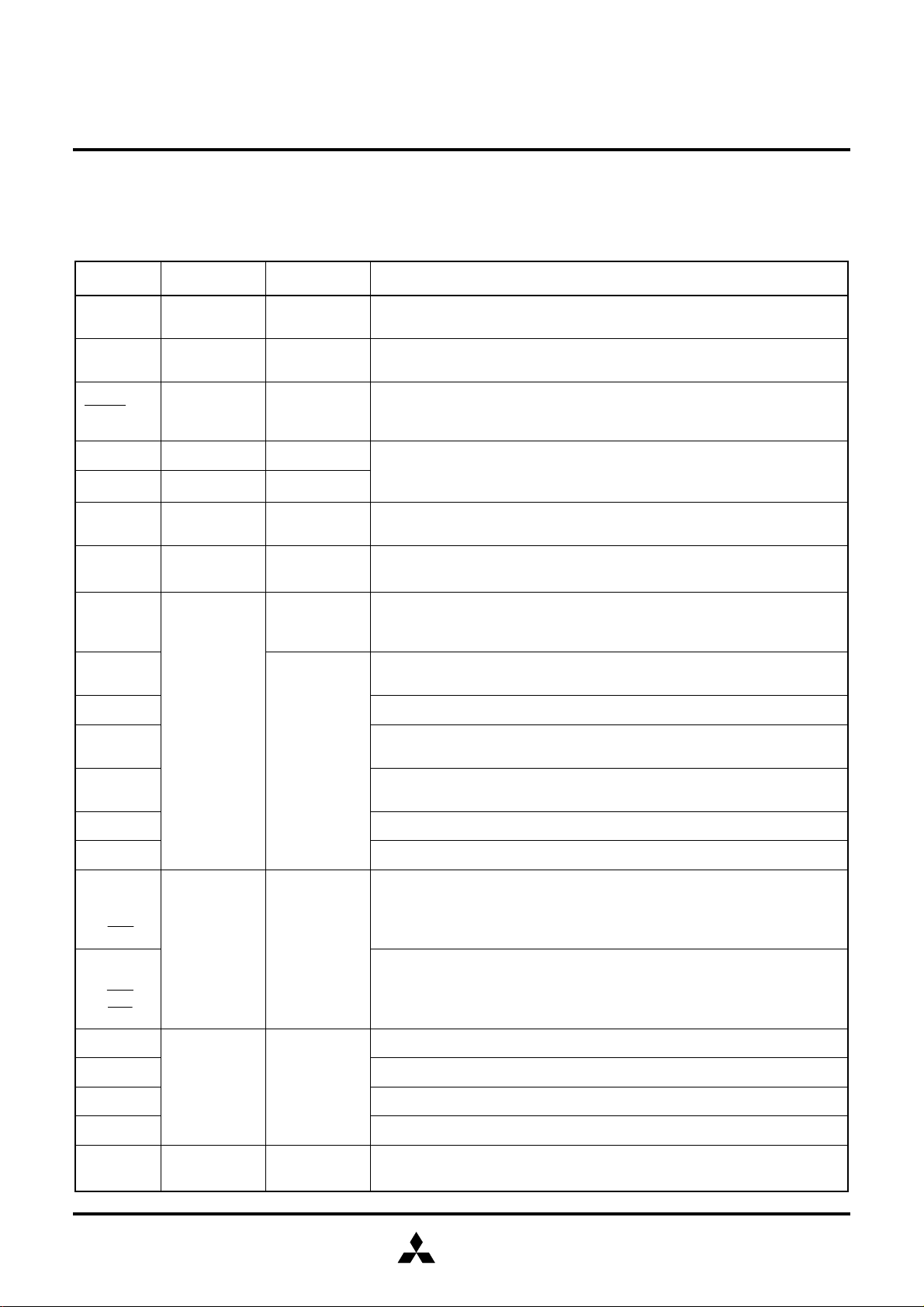
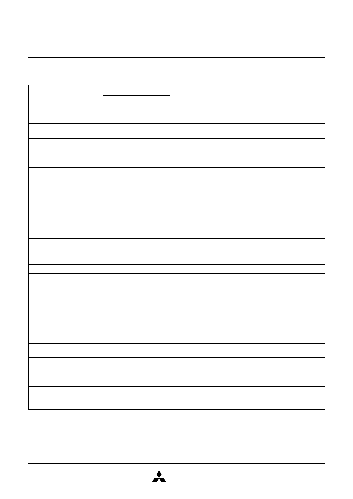
PIN DESCRIPTION
T a ble 1: Pin description
Pin Name Input/Output Description
MITSUBISHI MICROCOMPUTERS
7630 Group
V
AV
CC
, V
SS
SS
Power source
e
volta
Analog power
source volta
e
RESET Reset input Input
X
X
V
P0
P0
P1
P1
P1
P1
IN
OUT
REF
/AN0—
0
/AN
7
/INT
1
/INT
2
/TX
3
/CNTR
4
0
Clock input Input
Clock output Output
Reference volt-
e input
a
I/O port P0 I/O CMOS I/O ports or analog input ports
7
0
1
I/O port P1 I /O
0
Input Reference volta
Input
Power supply pins; apply 4.0 to 5.5 V to V
Ground pin for A-D converter. Connect to V
and 0 V to V
CC
SS
SS
Reset pin. This pin must be kept at “L” level for more than 2 µs, to enter the reset
state. If the crystal or ceramic resonator requires more time to stabilize, extend the
“L” level period.
Input and output pins of the internal clock
quartz–crystal resonator between the X
source is used, connect it to X
and leave X
IN
enerating circuit. Connect a ceramic or
and X
IN
pins. When an external clock
OUT
open.
OUT
e input pin for A-D converter
CMOS input port or external interrupt input port. The active ed
external interrupts can be selected. This pin will be used as V
ramming of One Time PROM Versions.
pro
e (rising or falling) of
pin during PROM
PP
CMOS I/O port or external interrupt input port. The active edge (rising or falling) of
external interrupts can be selected.
CMOS I/O port or input pin used in the bi-phase counter mode
CMOS I/O port or timer X input pin used for the event counter, pulse width measure-
ment and bi-phase counter mode
/CNTR
P1
5
/PWM
P1
6
P1
7
P2
0/SIN
P21/S
P22/S
P23/S
/URXD
P2
4
/UTXD
P2
5
P2
6/URTS
P27/U
P3
0
P3
/CTX
1
/CRX
P3
2
P3
—P3
3
P4
/KW0—
0
/KW
P4
7
OUT
CLK
RDY
CTS
1
I/O port P2
I/O port P3
4
I/O port P4 I /O
7
I/O
I/O
CMOS I/O port or timer Y input pin used for the event counter, pulse width and pulse
period measurement mode
CMOS I/O port or PWM output pin used in the PWM mode of timers 2 and 3
CMOS I/O port
CMOS I/O ports or clock synchronous serial I/O pins
CMOS I/O ports or asynchronous serial I/O pins
CMOS I/O port
CMOS I/O port or CAN transmit data pin
CMOS I/O port or CAN receive data pin
CMOS I/O port
CMOS I/O ports. These ports can be used for key-on wake-up when confi
ured as
inputs.
MITSUBISHI
ELECTRIC
3
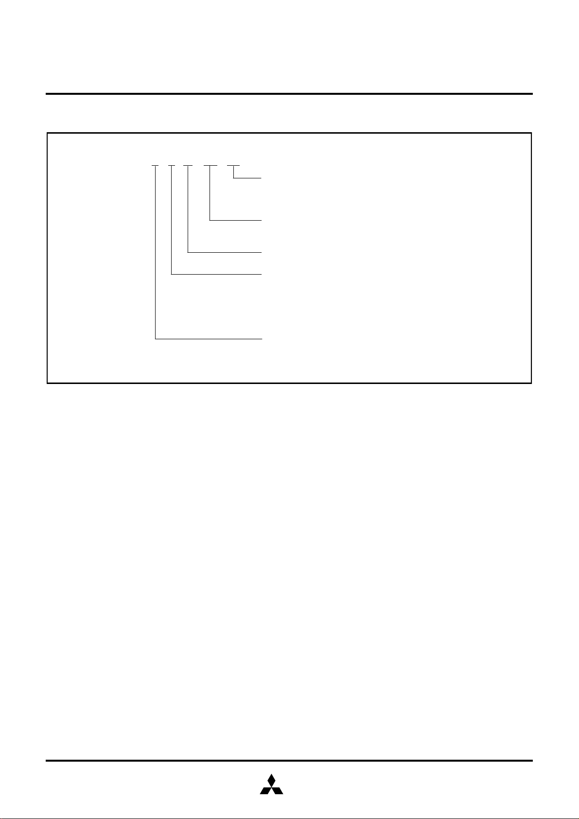
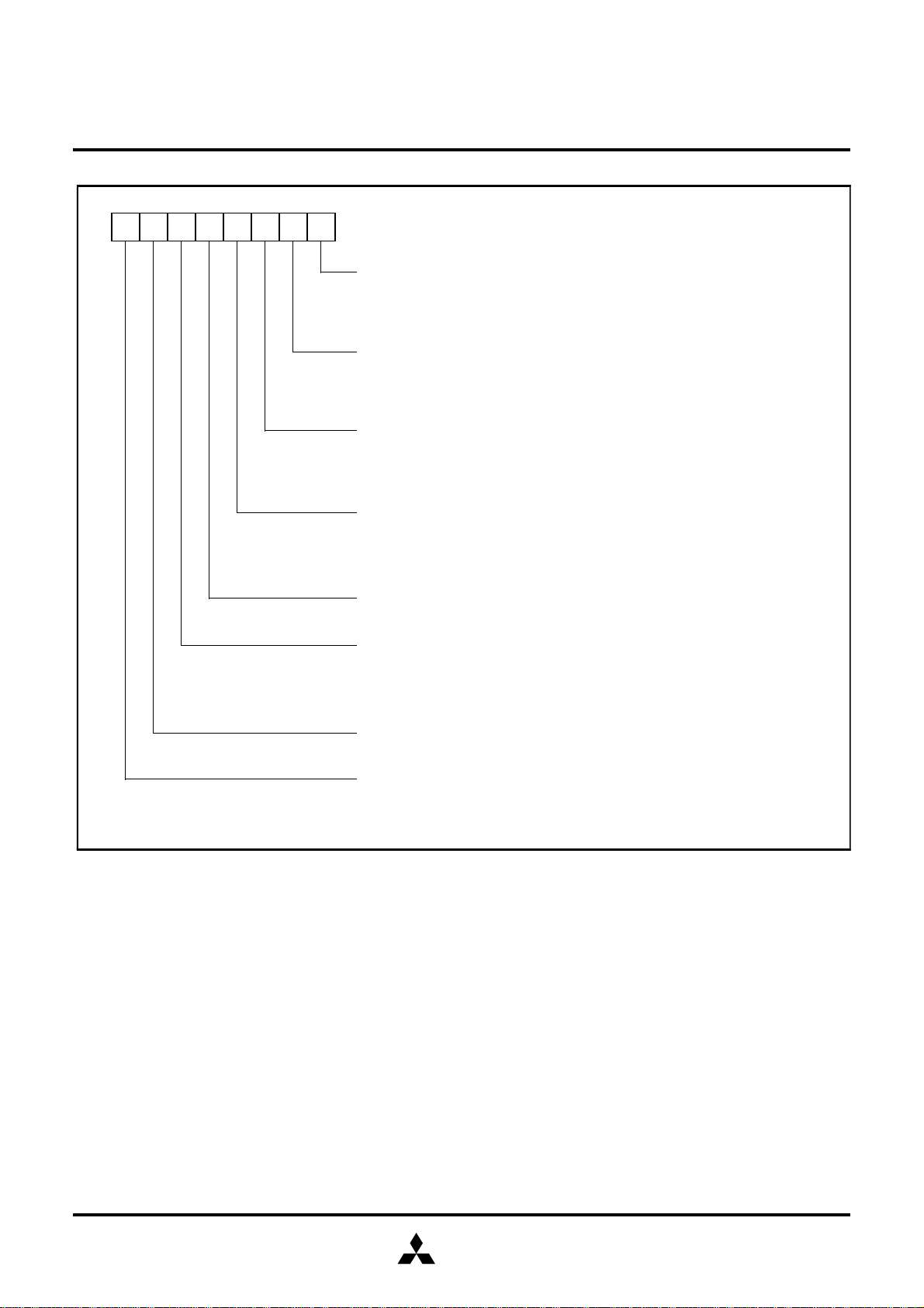
PART NUMBERING
g
g
g
Product M37630 M 4 T– XXX FP
MITSUBISHI MICROCOMPUTERS
7630 Group
SINGLE-CHIP 8-BIT CMOS MICROCOMPUTER
e type
Packa
FP: 44P6N-A packa
FS: 80D0 packa
ROM number
Omitted in One Time PROM version (blank) and EPROM version
T: Automotive use
ROM/PROM size
4: 16384 bytes
The first 128 bytes and the last 4 bytes of ROM are reserved areas.
They cannot be used.
e
e
Fig. 3 Part numbering
Memory type
M: Mask ROM version
E: EPROM or One Time PROM version
4
MITSUBISHI
ELECTRIC
GROUP EXPANSION
g
MITSUBISHI MICROCOMPUTERS
7630 Group
SINGLE-CHIP 8-BIT CMOS MICROCOMPUTER
Mitsubishi plans to expand the 7630 group as follows:
Memory Type
Support mask ROM, One Time PROM and EPROM versions.
ROM
External
60K
48K
32K
28K
24K
20K
M37630M4T
16K
12K
Mass product
M37630E4T
Memory Size
ROM/PROM size . . . . . . . . . . . . . . . . . . . . . . . . . . . . . 1 6 Kb ytes
RAM size. . . . . . . . . . . . . . . . . . . . . . . . . . . . . . . . . . . . 512 bytes
Package
44P6N-A . . . . . . . . . . . . . . . . .0.8mm-pitch plastic molded QFP
80D0 . . . . . . . . . . .0.8mm-pitch ceramic LCC (EPROM version)
Under development
8K
384 512 640 768 896 1024
RAM size (bytes)
Fig. 4 Memory expansion plan
Currently supported products are listed below:
Table 2: List of supported products
Product
M37630M4T-XXXFP Mask ROM version
M37630E4T-XXXFP 16384 512 44P6N-A One Time PROM version
M37630E4FP (16252) One Time PROM version (blank)
M37630E4FS 80D0 EPROM version
(P)ROM size (bytes)
ROM size for User ( )
RAM size (bytes) Packa
e Remarks
As of March 1998
MITSUBISHI
ELECTRIC
5
FUNCTIONAL DESCRIPTION
g
g
g
g
g
g
g
MITSUBISHI MICROCOMPUTERS
7630 Group
SINGLE-CHIP 8-BIT CMOS MICROCOMPUTER
Central Processing Unit (CPU)
The core of 7630 group microcomputers is the 7600 series CPU.
This core is based on the standard instruction set of 740 series;
however the performance is improved by allowin
same instructions as that of the 740 series in less cycles. Refer to
the 7600 Series Software Manual for details of the instruction set.
70
to execute the
CPU mode re
CPUM
Processor mode bits (set these bits to “00”)
b1 b0
0 0: Sin
0 1: Not used
1 0: Not used
1 1: Not used
Stack pa
Not used (“0” when read, do not write “1”)
Internal system clock selection bit
Not used (“0” when read, do not write “1”)
e selection bit
0 : 0 pa
1 : 1 pa
0 : φ=f(X
1 : φ=f(X
CPU Mode Register CPUM
The CPU mode register contains the stack page selection bit and
internal system clock selection bit. The CPU mode re
cated to address 0000
ister (address 000016)
le–chip mode
e
e
) divided by 2 (high–speed mode)
IN
) divided by 8 (middle–speed mode)
IN
.
16
ister is allo-
Fig. 5 Structure of CPU mode register
6
MITSUBISHI
ELECTRIC
MEMORY
g
g
g
g
MITSUBISHI MICROCOMPUTERS
7630 Group
SINGLE-CHIP 8-BIT CMOS MICROCOMPUTER
Special Function Register (SFR) Area
The special function register (SFR) area contains the registers
to functions such as I/O ports and timers.
relatin
RAM
RAM is used for data storage and for stack area of subroutine calls
and interrupts.
ROM
ROM is used for storing user’s program code as well as the interrupt vector area.
RAM area
RAM size
(byte)
192
256
384
512
640
768
896
1024
1536
2048
Address
XXXX
011F
015F
01DF
025F
02DF
035F
03DF
045F
06DF
085F
16
16
16
16
16
16
16
16
16
16
16
User RAM
Interrupt Vector Area
The interrupt vector area is for storing jump destination addresses
used at reset or when an interrupt is
enerated.
Zero Page
This area can be accessed most efficiently by means of the zero
e addressing mode.
pa
Special Page
This area can be accessed most efficiently by means of the s pecial
e addressing mode.
pa
0000
16
0040
0060
00FF
XXXX
0860
16
16
16
16
16
SFR area
CAN
SFRs
Zero page
ROM area
ROM size
(byte)
4096
8192
12288
16384
20480
24576
28672
32768
36864
40960
45056
49152
53248
57344
61440
Address
YYYY
F000
E000
D000
C000
B000
A000
9000
8000
7000
6000
5000
4000
3000
2000
1000
Fig. 6 Memory map diagram
Not used
Address
16
16
16
16
16
16
16
16
16
16
16
16
16
16
16
16
ZZZZ
F080
E080
D080
C080
B080
A080
9080
8080
7080
6080
5080
4080
3080
2080
1080
16
YYYY
ZZZZ
FF00
FFCA
FFFB
FFFC
FFFF
16
Reserved ROM area
16
16
16
Interrupt vector area
16
16
Reserved ROM area
16
Special page
16
16
16
16
16
16
ROM
16
16
16
16
16
16
16
16
16
MITSUBISHI
ELECTRIC
7
SPECIAL FUNCTION REGISTERS (SFR)
MITSUBISHI MICROCOMPUTERS
7630 Group
SINGLE-CHIP 8-BIT CMOS MICROCOMPUTER
0000
CPU mode register CPUM
16
0001
Not used
16
0002
Interrupt request register A IREQA
16
0003
Interrupt request register B IREQB
16
0004
Interrupt request register C IREQC
16
0005
Interrupt control register A ICONA
16
0006
Interrupt control register B ICONB
16
0007
Interrupt control register C ICONC
16
0008
Port P0 register P0
16
0009
Port P0 direction register P0D
16
000A
Port P1 register P1
16
000B
Port P1 direction register P1D
16
000C
Port P2 register P2
16
000D
Port P2 direction register P2D
16
000E
Port P3 register P3
16
000F
Port P3 direction register P3D
16
0010
Port P4 register P4
16
0011
Port P4 direction register P4D
16
0012
Serial I/O shift register SIO
16
0013
Serial I/O control register SIOCON
16
0014
A-D conversion register AD
16
0015
A-D control register ADCON
16
0016
Timer 1 T1
16
0017
Timer 2 T2
16
0018
Timer 3 T3
16
0019
Timer 123 mode register T123M
16
001A
Timer XL TXL
16
001B
Timer XH TXH
16
001C
Timer YL TYL
16
001D
Timer YH TYH
16
001E
Timer X mode register TXM
16
001F
Timer Y mode register TYM
16
0020
UART mode register UMOD
16
0021
UART baud rate generator UBRG
16
0022
UART control register UCON
16
0023
UART status register USTS
16
0024
UART transmit buffer register 1 UTBR1
16
0025
UART transmit buffer register 2 UTBR2
16
0026
UART receive buffer register 1 URBR1
16
0027
UART receive buffer register 2 URBR2
16
0028
Port P0 pull-up control register PUP0
16
0029
Port P1 pull-up control register PUP1
16
002A
Port P2 pull-up control register PUP2
16
002B
Port P3 pull-up control register PUP3
16
002C
Port P4 pull-up/down control register PUP4
16
002D
Interrupt polarity selection register IPOL
16
002E
Watchdog timer register WDT
16
002F
Polarity control register PCON
16
0030
CAN transmit control register CTRM
16
0031
CAN bus timing control register 1 CBTCON1
16
0032
CAN bus timing control register 2 CBTCON2
16
0033
CAN acceptance code register 0 CAC0
16
0034
CAN acceptance code register 1 CAC1
16
0035
CAN acceptance code register 2 CAC2
16
0036
CAN acceptance code register 3 CAC3
16
0037
CAN acceptance code register 4 CAC4
16
0038
CAN acceptance mask register 0 CAM0
16
0039
CAN acceptance mask register 1 CAM1
16
003A
CAN acceptance mask register 2 CAM2
16
003B
CAN acceptance mask register 3 CAM3
16
003C
CAN acceptance mask register 4 CAM4
16
003D
CAN receive control register CREC
16
003E
CAN transmit abort register CABORT
16
003F
Reserved
16
0040
CAN transmit buffer register 0 CTB0
16
0041
CAN transmit buffer register 1 CTB1
16
0042
CAN transmit buffer register 2 CTB2
16
0043
CAN transmit buffer register 3 CTB3
16
0044
CAN transmit buffer register 4 CTB4
16
0045
CAN transmit buffer register 5 CTB5
16
0046
CAN transmit buffer register 6 CTB6
16
0047
CAN transmit buffer register 7 CTB7
16
0048
CAN transmit buffer register 8 CTB8
16
0049
CAN transmit buffer register 9 CTB9
16
004A
CAN transmit buffer register A CTBA
16
004B
CAN transmit buffer register B CTBB
16
004C
CAN transmit buffer register C CTBC
16
004D
CAN transmit buffer register D CTBD
16
004E
Reserved
16
004F
Reserved
16
0050
CAN receive buffer register 0 CRB0
16
0051
CAN receive buffer register 1 CRB1
16
0052
CAN receive buffer register 2 CRB2
16
0053
CAN receive buffer register 3 CRB3
16
0054
CAN receive buffer register 4 CRB4
16
0055
CAN receive buffer register 5 CRB5
16
0056
CAN receive buffer register 6 CRB6
16
0057
CAN receive buffer register 7 CRB7
16
0058
CAN receive buffer register 8 CRB8
16
0059
CAN receive buffer register 9 CRB9
16
005A
CAN receive buffer register A CRBA
16
005B
CAN receive buffer register B CRBB
16
005C
CAN receive buffer register C CRBC
16
005D
CAN receive buffer register D CRBD
16
005E
Reserved
16
005F
Reserved
16
Fig. 7 Memory map of special register (SFR)
8
MITSUBISHI
ELECTRIC
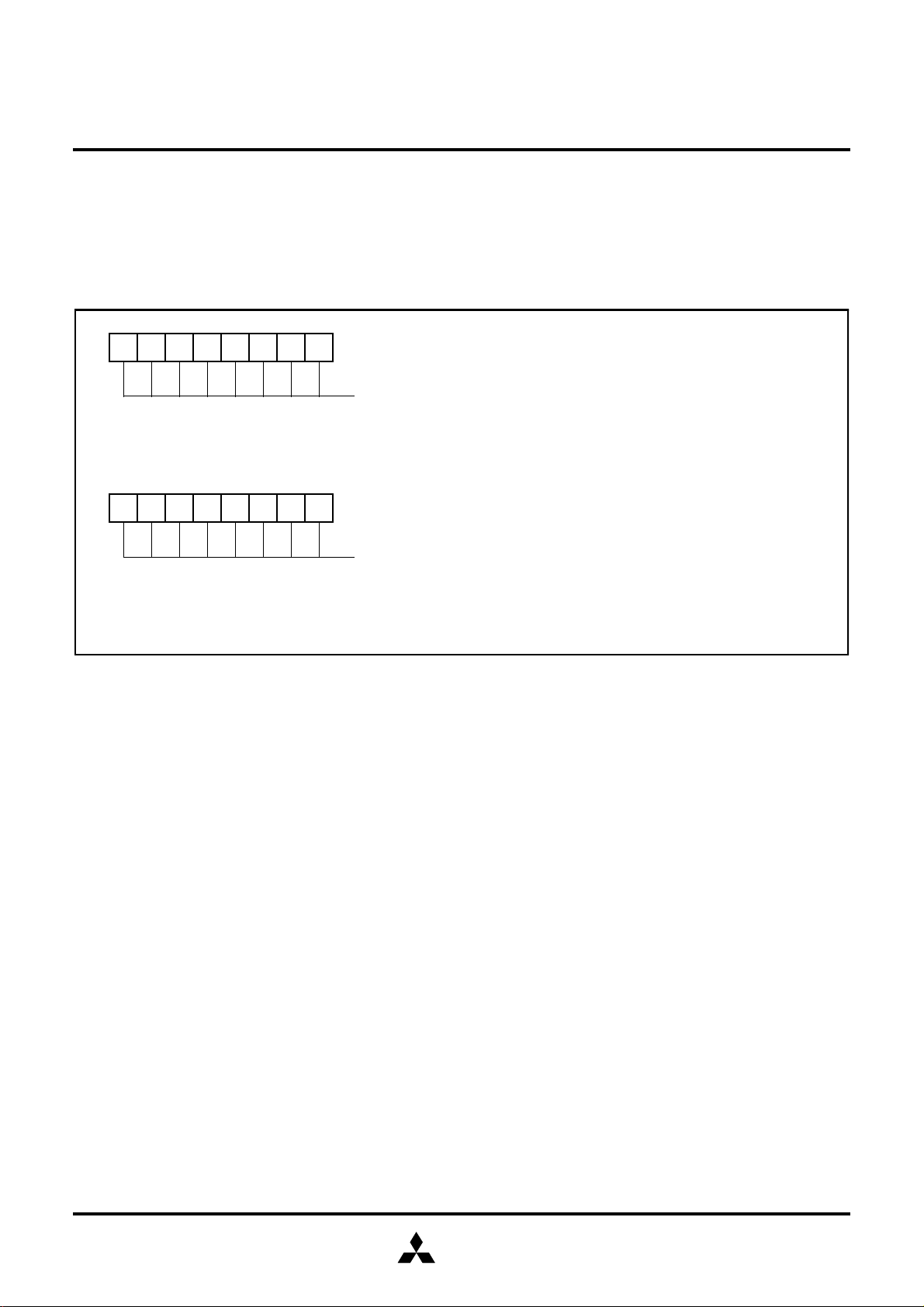
I/O PORTS
g
g
g
g
g
g
g
g
g
g
g
The 7630 group has 35 programmable I/O pins and one input pin
ed in five I/O ports (ports P0 to P4). The I/O ports are con-
arran
trolled by the correspondin
ters; each I/O pin can be controlled separately.
When data is read from a port confi
latch’s contents are read instead of the port level. A port confi
port registers and port direction regis-
ured as an output port, the port
ured
MITSUBISHI MICROCOMPUTERS
7630 Group
SINGLE-CHIP 8-BIT CMOS MICROCOMPUTER
as an input port becomes floatin
written to this port will affect the port latch only; the port remains
.
floatin
Refer to Structure of port- and port direction re
port I/Os (1) and Structure of port I/Os (2).
and its level can be read. Data
isters, Structure of
70
Port Pi re
Pi
Port Pij control bit (j = 0 to 7)
0 : “L” level
1 : “H” level
Note : The control bits corresponding to P10, P35, P36 and P37 are not used
70
Port Pi direction re
PiD
Port Pij direction control bit (j = 0 to 7)
0 : Port confi
1 : Port confi
Note : The direction control bits corresponding to P10, P11, P35, P36 and
Fig. 8 Structure of port- and port direction registers
ister (i = 0 to 4) (address 000816 + 2 · i)
(“0” when read, do not write “1”).
ister (i = 0 to 4) (address 000916 + 2 · i)
ured as input
ured as output
P3
are not used (“0” when read, do not write “1”). Port direction re-
7
gisters are undefined when read (write only).
MITSUBISHI
ELECTRIC
9
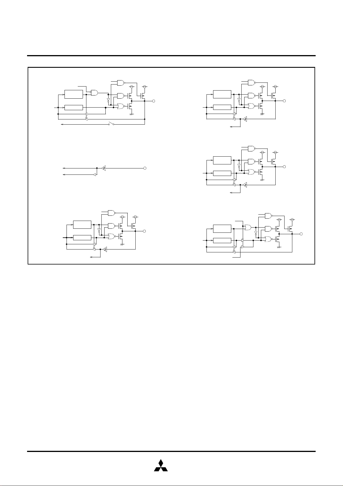
MITSUBISHI MICROCOMPUTERS
7630 Group
SINGLE-CHIP 8-BIT CMOS MICROCOMPUTER
(1) Ports P0
Data bus
/AN0 to P07/AN
0
Analog input selection
ADC input
(2) Port P11/INT
Interrupt input
Data bus
(3) Port P12/INT
Data bus
Direction
register
Port latch
0
1
Pull-up control bit
Direction
register
Port latch
7
Pull-up control bit
Analog input selection
(4) Port P13/TX
Timer bi-phase mode input
Data bus
0
Pull-up control bit
Port latch
direction
register
(5) Ports P14/CNTR0, P15/CNTR
Pull-up control bit
Direction
register
Data bus
Timer bi-phase mode input
Port latch
(6) Port P16/PWM
Pull-up control bit
PWM output enable
Direction
register
Data bus
Port latch
1
Interrupt input
Fig. 9 Structure of port I/Os (1)
PWM output
10
MITSUBISHI
ELECTRIC
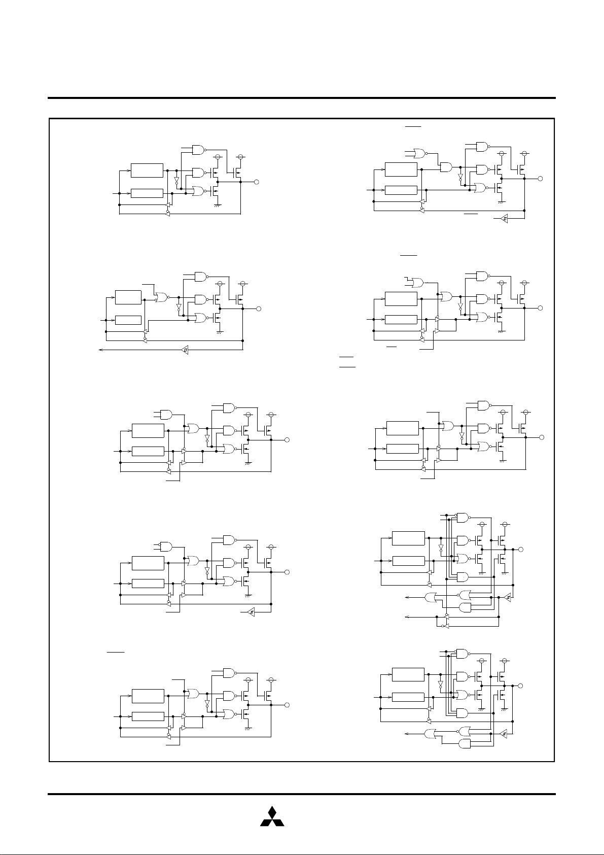
MITSUBISHI MICROCOMPUTERS
7630 Group
SINGLE-CHIP 8-BIT CMOS MICROCOMPUTER
(7) Ports P17, P30, P33, P3
Pull-up control bit
Direction
register
IN
Direction
register
Port latch
OUT
Port latch
Pull-up control bit
Direction
register
Port latch
Data bus
(8) Port P20/S
SIO Port Select
Data bus
SIO1 input
(9) Port P21/S
SIO port selection bit
Transmit complete signal
Data bus
4
Pull-up control bit
(12) Ports P24/URXD, P27/U
Transmission or reception* in
Transmit or receive* enable bit
Data bus
progress
Direction
register
Port latch
(13) Ports P25/UTXD, P26/U
Transmission or reception** in
Transmit or receive** enable bit
Data bus
(*) for U
CTS
(**) for U
RTS
progress
Direction
register
Port latch
U
or U
output
TXD
RTS
(14) Port P31/CTX
CAN port selection bit
Direction
register
Data bus
Port latch
CTS
Pull-up control bit
U
RTS
Pull-up control bit
Pull-up control bit
RXD
or U
CTS
input
SIO output
(10) Port P22/S
(11) Port P23/S
CLK
Clock selection bit
Port selection bit
direction
Data bus
SRDY output selection bit
Data bus
Port latch
SIO clock output
RDY
Direction
Port latch
SRDY output
Pull-up control bit
register
Pull-up control bit
register
Fig. 10 Structure of port I/Os (2)
External clock input
CTX output
(15) Port P3
/CRX
2
CAN dominant level control bit
Pull-up
/down control bit
Direction
register
Data bus
Port latch
CAN interrupt
CRX input
(16) Ports P40/KW0 to P47/KW
Key-on wake-up control bit
Pull-up
/down control bit
Direction
register
Data bus
Key-on wake-up interrupt
Port latch
7
MITSUBISHI
ELECTRIC
11
MITSUBISHI MICROCOMPUTERS
g
g
g
g
g
g
g
g
g
g
7630 Group
SINGLE-CHIP 8-BIT CMOS MICROCOMPUTER
Port Pull-up/pull-down Function
Each pin of ports P0 to P4 except P11 is equipped with a programmable pull-up transistor. P3
equipped with pro
pull-up function of P0 to P3 can be controlled by the correspondin
70
70
70
70
rammable pull-down transistors as well. The
/CRX and P40/KW0 to P47/KW7 are
2
Port Pi pull-up control re
PUP0, PUP2
Pij pull-up transistor control bit (j = 0 to 7)
0 : Pull-up transistor disabled
1 : Pull-up transistor enabled
Port P1 pull-up control register (address 002916)
PUP1
Not used (“0” when read, do not write “1”)
pull-up transistor control bit (j = 2 to 7)
P1
j
Port P3 pull-up control register (address 002B16)
PUP3
P3j pull-up transistor control bit (j = 0, 1)
P32 pull-up/down transistor control bit
pull-up transistor control bit (j = 3, 4)
P3
j
Not used (“0” when read, do not write “1”)
Port P4 pull-up/down control re
PUP4
port pull-up control registers (see Structure of port pull-up/down
control re
can be controlled by the correspondin
ters to
polarity control re
isters). The pull-up/down function of ports P32 and P4
port pull-up/pull-down regis-
ether with the polarity control register (see Structure of
ister).
ister (address 002816 + i) (i = 0, 2)
ister (address 002C16)
P4j pull-up/down transistor control bit (j = 0 to 7)
0 : Pull-up/down transistor disabled
1 : Pull-up/down transistor enabled
Fig. 11 Structure of port pull-up/down control regist ers
70
Polarity control register (address 002F16)
PCON
Key-on wake-up polarity control bit
0 : Low level active
1 : Hi
CAN module dominant level control bit
0 : Low level dominant
1 : Hi
Not used (undefined when read)
Fig. 12 Structure of polarity control register
h level active
h level dominant
12
MITSUBISHI
ELECTRIC

MITSUBISHI MICROCOMPUTERS
g
g
g
g
g
g
g
g
g
g
7630 Group
SINGLE-CHIP 8-BIT CMOS MICROCOMPUTER
Port Overvoltage Application
When configured as input ports, P1 to P4 may be subjected to over-
e (VI>VCC) if the input current to the applicable port is limited
volta
to the specified values (see “Table 8:”). Use a serial resistor of
appropriate size to limit the input current. To estimate the resistor
value, assume the port volta
Notes:
• Subjectin
Assure to keep V
ports to overvoltage may effect the supply voltage.
CC
e to be VCC at overvoltage condition.
and VSS within the target limits.
• Avoid to subject ports to overvolta
5.5 V.
• The overvolta
the internal port protection circuits has a ne
ports noise immunity. Therefore, careful and intense testin
the tar
“countermeasures a
manual.
• Port P0 must not be subjected to overvolta
e condition causing input current flowing through
et system’s noise immunity is required. Refer to the
ainst noise” of the corresponding users
e causing VCC to rise above
ative effect on the
e conditions.
of
MITSUBISHI
ELECTRIC
13

INTERRUPTS
g
g
g
g
g
g
g
g
g
g
g
g
There are 24 interrupts: 6 external, 17 internal, and 1 software.
Interrupt Control
Each interrupt except the BRK instruction interrupt has both an
interrupt request bit and an interrupt enable bit, and is controlled by
the interrupt disable fla
interrupt request and enable bits are “1” and the interrupt dis-
in
able fla
software. Interrupt request bits can be cleared by software but cannot be set by software. The BRK instruction interrupt and reset cannot be disabled with any fla
except the BRK instruction interrupt and reset. If several interrupt
requests occur at the same time, the interrupt with the hi
ity is accepted first.
is “0”. Interrupt enable bits can be cleared or set by
Interrupt Operation
Upon acceptance of an interrupt, the following operations are automatically performed.
1. The processin
. An interrupt occurs when the correspond-
or bit. The I flag disables all interrupts
hest prior-
being executed is stopped.
MITSUBISHI MICROCOMPUTERS
7630 Group
SINGLE-CHIP 8-BIT CMOS MICROCOMPUTER
2. The contents of the pro
ister are automatically pushed onto the stack.
re
3. Concurrently with the push operation, the interrupt jump
destination address is read from the vector table into the
ram counter.
pro
4. The interrupt disable fla
request bit is cleared.
Notes on use
When the active edge of an external interrupt (INT0, INT1, CNTR0,
, CWKU or KOI) is changed, the corresponding interrupt
CNTR
1
request bit may also be set. Therefore, take the followin
(1) Disable the external interrupt which is selected.
(2) Chan
(3) Clear the interrupt request bit to “0”.
(4) Enable the external interrupt which is selected.
e the active edge in interrupt edge selection register.
(in the case of CNTR
: Timer Y mode register)
CNTR
1
ram counter and processor status
is set and the corresponding interrupt
sequence.
: Timer X mode register; in the case of
0
14
MITSUBISHI
ELECTRIC
.
g
g
g
g
g
g
g
g
g
g
g
g
g
g
g
Table 3: Interrupt vector addresses and priority
MITSUBISHI MICROCOMPUTERS
7630 Group
SINGLE-CHIP 8-BIT CMOS MICROCOMPUTER
Interrupt source Priority
Reset (Note 2)
Watchdo
INT
INT
CAN
transmit
timer 2
0
1
successful
CAN successful
receive
CAN overrun 7
CAN error
passive
CAN error bus off 9
CAN wake up 10
Timer X 11
Timer Y 12
Timer 1 13
Timer 2 14
Timer 3 15
0
CNTR
CNTR
1
16
17
UART receive 18
UART transmit 19
UART transmit
buffer empty
UART receive
error
20
21
Vector Address (Note 1)
h Low
Hi
1
3
4
5
6
8
FFFB
FFF9
FFF7
FFF5
FFF3
FFF1
FFEF
FFED
FFEB
FFE9
FFE7
FFE5
FFE3
FFE1
FFDF
FFDD
FFDB
FFD9
FFD7
FFD5
FFD3
16
16
16
16
16
16
16
16
16
16
16
16
16
16
16
16
16
16
16
16
16
FFFA
FFF8
FFF6
FFF4
FFF2
FFF0
FFEE
FFEC
FFEA
FFE8
FFE6
FFE4
FFE2
FFE0
FFDE
FFDC
FFDA
FFD8
FFD6
FFD4
FFD2
16
16
16
16
16
16
16
16
16
16
16
16
16
16
16
16
16
16
16
16
16
Interrupt Request Generatin
Conditions
At Reset Non-maskable
At Watchdog timer underflow Non-maskable
At detection of either rising or falling
e of INT0 interrupt
ed
At detection of either rising or falling
e of INT1 interrupt
ed
At CAN module successful
transmission of messa
e
At CAN module successful reception
of messa
e
If CAN module receives message
when receive buffers are full.
When CAN module enters into error
passive state
When CAN module enters into bus
off state
When CAN module wakes up via
CAN bus
At Timer X underflow or overflow
At Timer Y underflow
At Timer 1 underflow
At Timer 2 underflow
At Timer 3 underflow
At detection of either rising or falling
e in CNTR0 input
ed
At detection of either rising or falling
e in CNTR1 input
ed
At completion of UART receive Valid when UART is selected
At completion of UART transmit Valid when UART is selected
At UART transmit buffer empty Valid when UART is selected
When UART reception error occurs. Valid when UART is selected
Remarks
External Interrupt
(active ed
e selectable)
External Interrupt
(active ed
e selectable)
Valid when CAN module is
activated and request transmit
Valid when CAN module is
activated
Valid when CAN module is
activated
Valid when CAN module is
active
Valid when CAN module is
active
External Interrupt
(active ed
e selectable)
External Interrupt
(active ed
e selectable)
Serial I/O 22
A-D conversion 23
Key-on wake-up 24
BRK instruction 25
FFD1
FFCF
FFCD
FFCB
16
16
16
16
FFD0
FFCE
FFCC
FFCA
At completion of serial I/O data
16
transmit and receive
At completion of A-D conversion
16
At detection of either rising or falling
16
16
e of P4 input
ed
At BRK instruction execution Non-maskable
Valid when serial I/O is
selected
External Interrupt
(active edge selectable)
Notes 1: Vector addresses contain interrupt jump destination address
2 : Reset function in the same way as an interrupt with the hi
hest priority
MITSUBISHI
ELECTRIC
15

Interrupt request bit
g
g
g
g
g
g
Interrupt enable bit
Interrupt disable flag I
MITSUBISHI MICROCOMPUTERS
7630 Group
SINGLE-CHIP 8-BIT CMOS MICROCOMPUTER
BRK instruction
Reset
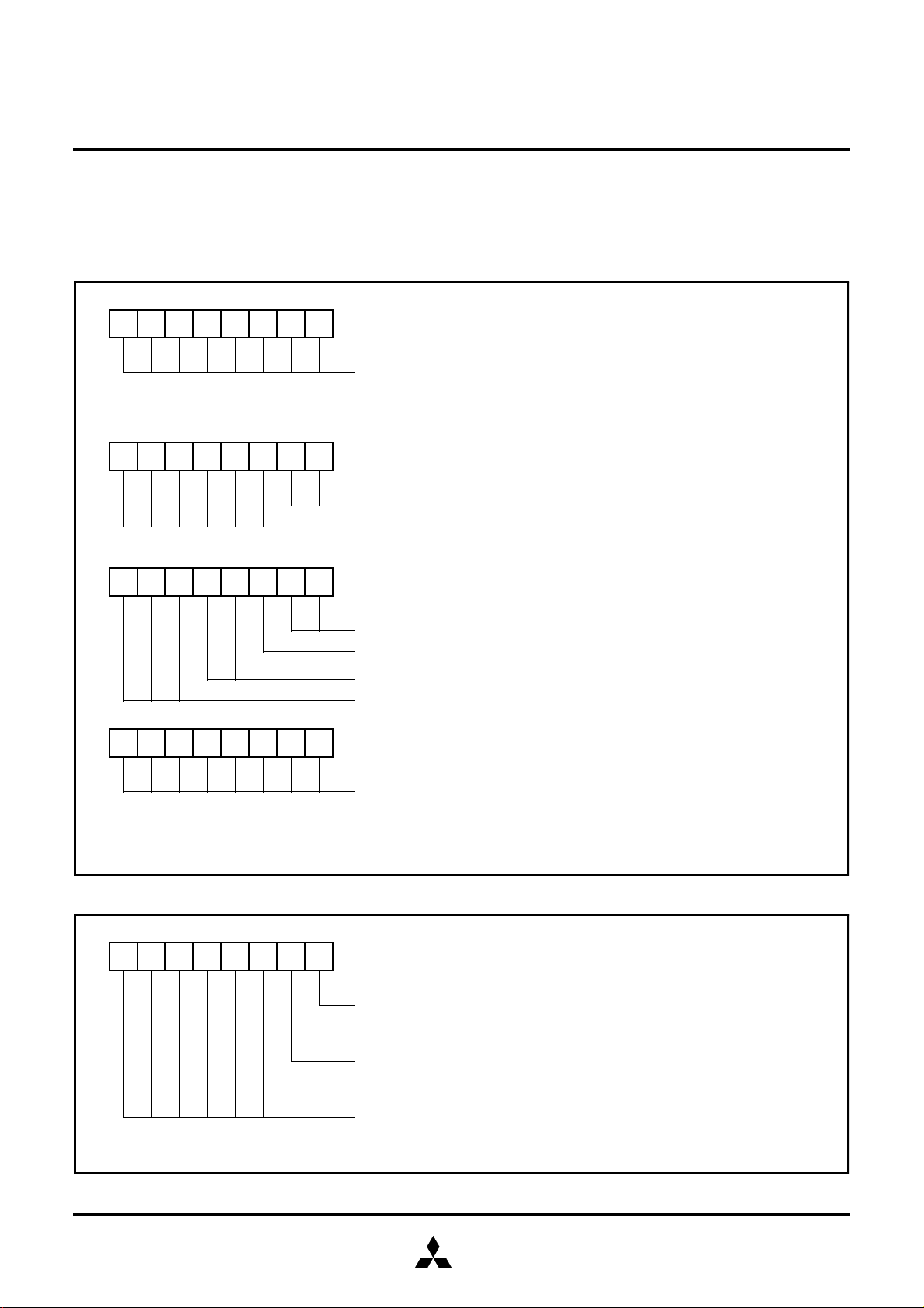
Fig. 13 Interrupt control
For the external interrupts INT0 and INT1, the active edge causin
the interrupt request can be selected by the INT0 and INT1 interrupt
e selection bits of the interrupt polarity selection register (IPOL);
ed
please refer to Fi
. 14 below.
70
Interrupt polarity selection re
IPOL
Not used (returns to “0” when read, do not write “1” in this bit)
interrupt edge selection bit
INT
0
interrupt edge selection bit
INT
1
Not used (returns to “0” when read, do not write “1” in these bits)
0 : Fallin
1 : Risin
Fig. 14 Structure of interrupt polarity selection register
Interrupt request
ister (Address 002D16)
edge active
edge active
16
MITSUBISHI
ELECTRIC

MITSUBISHI MICROCOMPUTERS
g
g
g
g
g
g
g
7630 Group
SINGLE-CHIP 8-BIT CMOS MICROCOMPUTER
7
7
7
0 : No interrupt request
1 : Interrupt requested
Interrupt request re
0
(address 0002
ister A
IREQA
Not used
(returns to ”0” when read)
External interrupt INT
External interrupt INT
CAN successful transmission
request bit
0
request bit
1
interrupt request bit
CAN successful receive
interrupt request bit
CAN overrun interrupt request bit
CAN error passive
interrupt request bit
CAN bus off interrupt request bit
0
Interrupt request register B
(address 0003
16
IREQB
CAN wake up
interrupt request bit
Timer X interrupt request bit
Timer Y interrupt request bit
Timer 1 interrupt request bit
Timer 2 interrupt request bit
Timer 3 interrupt request bit
interrupt request bit
CNTR
0
interrupt request bit
CNTR
1
Interrupt request re
0
(address 0004
ister C
16
IREQC
UART receive complete
(receive buffer full)
interrupt request bit
UART transmit complete
(transmit re
ister empty)
interrupt request bit
UART transmit buffer empty
interrupt request bit
UART receive error interrupt
request bit
Serial I/O interrupt request bit
AD conversion complete
interrupt request bit
Key-on wake-up interrupt request bit
Not used (returns to ”0” when read)
)
16
7
Interrupt control re
0
(address 0005
ister A
16
)
ICONA
Not used (returns to ”0” when read)
External interrupt INT
External interrupt INT
enable bit
0
enable bit
1
CAN successful transmission
interrupt enable bit
CAN successful receive
interrupt enable bit
CAN overrun interrupt enable bit
CAN error passive
interrupt enable bit
CAN bus off interrupt enable bit
7 0
)
Interrupt control re
(address 0006
ICONB
ister B
16
)
CAN wake–up interrupt enable bit
Timer X interrupt enable bit
Timer Y interrupt enable bit
Timer 1 interrupt enable bit
Timer 2 interrupt enable bit
Timer 3 interrupt enable bit
interrupt enable bit
CNTR
0
CNTR1 interrupt enable bit
)
7 0
Interrupt control re
(address 0007
ister C
16
)
ICONC
UART receive complete
(receive buffer full)
interrupt enable bit
UART transmit complete
(transmit re
ister empt y)
interrupt enable bit
UART transmit buffer empty
interrupt enable bit
UART receive error interrupt
enable bit
Serial I/O interrupt enable bit
AD conversion complete
interrupt enable bit
Key-on wake-up interrupt enable bit
Not used (returns to ”0” when read)
0: Interrupt disabled
1: Interrupt enabled
Fig. 15 Structure of interrupt request and control registers A, B and C
MITSUBISHI
ELECTRIC
17

KEY-ON WAKE-UP
g
g
g
“Key-on wake-up” is one way of returning from a power-down state
caused by the STP or WIT instruction. Any terminal of port P4 can
be used to
active polarity can be selected by the key-on wake-up polarity con-
Fig. 16 Block diagram of key-on wake-up circuit
enerate the key-on wake-up interrupt request. The
key-on wake-up control bit
P4D
j
PUP4
j
port P4j/KW
j
j = 0 to 7
MITSUBISHI MICROCOMPUTERS
7630 Group
SINGLE-CHIP 8-BIT CMOS MICROCOMPUTER
trol bit of PCON (see Fi
active level applied, the key-on wake-up interrupt request will be set
to “1”. Please refer to Fi
…
port P4j I/O circuit
. 12). If any pin of port P4 has the selected
. 16.
key-on wake-up interrupt
18
MITSUBISHI
ELECTRIC

TIMERS
g
g
g
g
g
g
g
g
g
g
g
g
g
g
g
g
g
The 7630 group has five timers: two 16-bit timers and three 8-bit
timers . All these timers will be described in detail below.
TYM
1,0
edge detector
sign generator
edge detector
“1”
“0”
TXM
TXM
5,4
“00”, “11”
“01”
“10”
direction
control
down
“00”, “10”,
“01”
TXM
5, 4
6
P13/TX
P14/CNTR
φ
0
0
1/4
1/16
1/64
1/128
“00”
“01”
“10”
“11 ”
MITSUBISHI MICROCOMPUTERS
7630 Group
SINGLE-CHIP 8-BIT CMOS MICROCOMPUTER
16-bit Timers
Timers X and Y are 16-bit timers with multiple operating modes.
. 17.
TX
H
counter (8)
TX
H
latch (8)
TX interrupt request
CNTR0 interrupt request
TXM
count
“11”
7
Please refer to Fi
TXL latch (8)
TXL counter (8)
TXM
=“11”
TYM
3, 2
“1”
5, 4
TYM
“0x”, “11”
“0”
6
TYM
5, 4
“10”
rising edge detector
falling edge detector
P1
/CNTR
5
“00”
1/2
“01”
1/8
“10”
1/32
“11”
1/64
1
Fig. 17 Block diagram of timers X and Y (φ is internal system clock)
Timer X
Timer X is a 16-bit timer with a 16-bit reload latch supporting the fol-
operating modes:
lowin
(1) Timer mode
(2) Bi-phase counter mode
(3) Event counter mode
(4) Pulse width measurement mode
These modes can be selected by the timer X mode re
In the timer- and pulse width measurement mode, the timer’s count
source can be selected by the timer X count source selection bits of
the timer Y mode re
for the TXM and TYM bit assi
ister (TYM). Please refer to the Figures below
nment.
On read or write access to timer X, note that the hi
order bytes must be accessed in the specific order.
Write method
When writing to the timer X, write the low-order byte first. The data
written is stored in a temporary re
ister which is assigned to the
ister (TXM).
h-order and low-
latch (8)
TY
TYM
L
7
TYL counter (8)
TYM
TYM
5, 4
5, 4
=“11”
=“01”
same address as TX
finished, the data is placed in the timer X hi
and the low-order byte is transferred from its temporary re
the timer X low-order reload latch. Dependin
latch (8)
TY
H
TY
counter (8)
H
“0x”,
“10”
TYM
. Next, write the high-order byte. When this is
L
TY interrupt request
“11 ”
CNTR1 interrupt request
5, 4
h-order reload latch
ister to
on the timer X write
control bit, the latch contents are reloaded to the timer immediately
(write control bit = “0”) or on the next timer underflow ( write control
bit = “1”).
Read method
When readin
causes the timer X hi
temporary re
the timer X, read the high-order byte first. This
h- and low-order bytes to be transferred to
isters being assigned to the same addresses as TX
and TXL. Next, read the low-order byte which is read from the temporary re
read durin
ister. This method assures the correct timer value can be
the timer count operation.
Timer X count stop control
Re
ardless of the actual operating mode, timer X can be stopped
by settin
the timer X count stop bit (bit 7 of the timer X mode regis-
ter) to “1”.
H
MITSUBISHI
ELECTRIC
19

MITSUBISHI MICROCOMPUTERS
g
g
g
g
g
g
g
g
g
g
g
g
g
g
g
g
g
g
g
g
7630 Group
SINGLE-CHIP 8-BIT CMOS MICROCOMPUTER
70
Fig. 18 Structure of Timer X mode register
Timer X mode re
TXM
Timer X data write control bit
0 : Data is written to latch and timer
1 : Data is written to latch only
Not used (“0” when read, do not write “1”)
Timer X mode bits
b5 b4
0 0: Timer mode
0 1: Bi-phase counter mode
1 0: Event counter mode
1 1: Pulse width measurement mode
polarity selection bit
CNTR
0
0 : For event counter mode, rising edge active
For interrupt request, fallin
For pulse width measurement mode, measure “H” period
1 : For event counter mode, fallin
For interrupt request, risin
For pulse width measurement mode, measure “L” period
Timer X stop control bit
0 : Timer countin
1 : Timer stopped
Timer Y
Timer Y is a 16 bit timer with a 16-bit reload latch supporting the fol-
operating modes:
lowin
(1) Timer mode
(3) Event counter mode
(5) Pulse period measurement mode
(6) H/L pulse width measurement mode
These modes can be selected by the timer Y mode re
In the timer, pulse period- and pulse width measurement modes’
the timer’s count source can be selected by the timer Y count
source selection bits. Please refer to Fi
On read or write access to timer Y, note that the hi
order bytes must be accessed in a specific order.
Write method
When writin
ten is stored in a temporary re
to timer Y, write the low-order byte first. The data writ-
. 19.
ister wh ich is a ssigned to the same
ister (TYM).
h-order and low-
ister (address 001E16)
edge active
edge active
edge active
address as TY
ished, the data is placed in the timer Y hi
the low-order byte is transferred from its temporary re
timer Y low-order reload latch.
Read method
When readin
causes the timer Y hi
temporary re
and TYL. Next, read the low-order byte which is read from the temporary re
read durin
Timer Y count stop control
Re
ardless of the actual operating mode, timer Y can be stopped
by settin
ter) to “1”.
. Next, write the high-order byte. When this is fin-
L
the timer Y, read the high-order byte first. This
h- and low-order bytes to be transferred to
isters being assigned to the same addresses as TY
ister. This method assures the correct timer value can be
timer count operation.
the timer Y count stop bit (bit 7 of the timer Y mode regis-
h-order reload latch and
ister to the
H
20
MITSUBISHI
ELECTRIC

MITSUBISHI MICROCOMPUTERS
g
g
g
g
g
g
g
g
g
g
g
g
g
g
g
g
g
g
g
g
g
g
7630 Group
SINGLE-CHIP 8-BIT CMOS MICROCOMPUTER
70
Timer Y mode re
TYM
Timer X count source selection bits
b1 b0
0 0: φ divided by 4
0 1: φ divided by 16
1 0: φ divided by 64
1 1: φ divided by 128
Timer Y count source selection bits
b3 b2
0 0: φ divided by 2
0 1: φ divided by 8
1 0: φ divided by 32
1 1: φ divided by 64
Timer Y operation mode bits
b5 b4
0 0: Timer mode
0 1: Pulse period measurement mode
1 0: Event counter mode
1 1: H/L pulse width measurement mode
polarity selection bit
CNTR
1
0 : For event counter mode, rising edge active
1 : For event counter mode, fallin
Timer Y stop control bit
0 : Timer countin
1 : Timer stopped
ister (address 001F16)
For interrupt request, fallin
For pulse period measurement mode, refer to fallin
For interrupt request, risin
For pulse period measurement mode, refer to risin
edge active
edges
edge active
edge active
edges
Fig. 19 Structure of timer Y mode register (φ is internal system clock)
Operating Modes
(1) Timer mode
This mode is available with timer X and timer Y.
• Count source
The count source for timer X and Y is the output of the correspondin
timer Y mode re
• Operation
Both timers X and Y are down counters. On a timer underflow,
the correspondin
contents of the correspondin
the counters and countin
clock divider. The division ratio can be selected by the
ister.
timer interrupt request bit will be set to “1”, the
timer latches will be reloaded to
continues.
(2) Bi-phase counter mode (quadruplicate)
This mode is available with timer X only.
• Count source
The count sources are P1
• Operation
Timer X will count both risin
(see above). Refer to Timer X bi-phase counter mode operation
for the timin
chart of the bi-phase counter mode.
/CNTR0 and the P13/TX0 pins.
4
and falling edges on both input pins
Table 4: Timer X count direction in Bi-phase counter mode
The count direction is determined by the ed
of count source inputs and may chan
tion. Refer to the table below.
P1
/TX
3
0
↑ Ed
e
↓ Ed
e
L
HUp
L
H Down
On a timer over- or underflow, the correspondin
request bit will be set to “1” and countin
P14/CNTR
LUp
H Down
L Down
HUp
e
↑ Ed
e
↓ Ed
0
Count direction
e polarity and level
e during the count opera-
Down
Up
interrupt
continues.
MITSUBISHI
ELECTRIC
21

g
g
g
g
g
g
g
g
g
g
g
g
g
g
g
g
g
g
g
g
g
g
g
g
g
g
g
g
P13/TX0 input signal
P1
/CNTR0 input signal
4
TX counter
MITSUBISHI MICROCOMPUTERS
7630 Group
SINGLE-CHIP 8-BIT CMOS MICROCOMPUTER
count direction
down up
Fig. 20 Timer X bi-phase counter mode operation
(3) Event counter mode
This mode is available with timer X and timer Y.
• Count source
The count source for timer X is the input si
nal to the P14/CNTR
pin and for timer Y the input signal to P15/CNTR1 pin.
• Operation
The timer counts down. On a timer underflow, the correspondin
timer interrupt request bit will be set to “1”, the contents of the
correspondin
countin
timer latches will be reloaded to the counters and
continues. The active edge used for counting can be
selected by the polarity selection bit of the correspondin
/CNTR0 or P15/CNTR1. These bits are part of TXM (Structure
P1
4
of Timer X mode re
ister (f is internal system clock)) registers.
re
ister) and TYM (Structure of timer Y mode
(4) Pulse width measurement mode
This mode is available with timer X only.
• Count source
The count source is the output of timer X clock divider. The division ratio can be selected by the timer Y mode re
ister.
• Operation
The timer counts down while the input si
/CNTR0 matches the active polarity selected by the CNTR
P1
4
nal level on
polarity selection bit of TXM (Structure of Timer X mode register). On a timer underflow, the timer X interrupt request bit will be
set to “1”, the contents of the timer latches are reloaded to the
counters and countin
from active polarity (as selected), the CNTR
continues. When the input level changes
interrupt request bit
0
will be set to “1.” The measurement result may be obtained by
timer X during interrupt service.
readin
(5) Pulse period measurement mode
This mode is available with timer Y only.
• Count source
The count source is the output of timer Y clock divider.
pin
• Operation
The active ed
by CNTR
e of input signal to be measured can be selected
polarity selection bit (Fig. 18). When this bit is set to
1
“0”, the time between two consecutive fallin
0
input to P1
/CNTR1 pin will be measured, when the polarity bit is
5
set to “1”, the time between two consecutive risin
measured.
The timer counts down. On detection of an active ed
nal, the contents of the TY counters will be transferred to tem-
si
porary re
isters assigned to the same addresses as TY. At the
same time, the contents of TY latches will be reloaded to the
counters and countin
also causes the CNTR
continues. The active edge of input signal
interrupt request bit to be set to “1”. The
1
measurement result may be obtained by readin
interrupt service.
(6) H/L pulse width measurement mode
This mode is available with timer Y only.
• Count source
The count source is the output of the timer Y’s clock divider.
• Operation
0
This mode measures both the “H” and “L” periods of a si
input to P1
(risin
/CNTR1 pin continuously. On detection of any edge
5
or falling) of input signal to P15/CNTR1 pin, the contents of
timer Y counters are stored to temporary re
ned to the same addresses as timer Y. At the same time,
assi
the contents of timer Y latches are reloaded to the counters and
countin
continues. The detection of an edge causes the
CNTR1 interrupt request bit to be set to “1” as well. The result of
measurement may be obtained by readin
rupt service. This read access will address the temporary re
ters. On a timer underflow, the timer Y interrupt request bit will
be set to “1”, the contents of timer Y latches will be transferred to
the counters and countin
continues.
edges of the signal
edges will be
e of input
timer Y durin
nal
isters which are
timer Y during inter-
is-
22
MITSUBISHI
ELECTRIC

TIMER 1, TIMER 2, TIMER 3
g
g
g
g
g
g
g
g
Timers 1 to 3 are 8-bit timers with 8-bit reload latches and one common pre-divider. Timer 1 can operate in the timer mode only,
T123M
φ
1
1/8
1/32
1/128
“00
“01”
“10”
“11”
67
”
“1” “0”
MITSUBISHI MICROCOMPUTERS
7630 Group
SINGLE-CHIP 8-BIT CMOS MICROCOMPUTER
whereas timers 2 and 3 can be used to generate a PWM output signal timin
as well. Timers 1 to 3 are down count timers. See Fig. 21.
T1 latch (8)
T1 counter (8)
T2 latch (8)
T1 interrupt
T123M
3
“0” “1”
T123M
1
“1” “0”
T123M
4
“0” “1”
T123M
1
P16/PWM
P1D
T123M
6
1
P16 latch
Fig. 21 Block diagram of timers 1 to 3 (φ is internal system clock)
Timer 1
The count source of timer 1 is the output of timer 123 pre-divider.
The division ratio of the pre-divider can be selected by the predivider division ratio bits of timer 123 mode re
to Timer 123 mode re
ister configuration (f is internal system clock).
ister (T123M). Refer
On a timer 1 underflow, the timer 1 interrupt request bit will be set to
“1”.
to timer 1 initializes the latch and counter.
Writin
Timers 2 and 3
The count source of timers 2 and 3 can be either the output of the
timer 123 pre-divider or the timer 1 underflow. The count source can
T2 counter (8)
T3 latch (8)
T3 counter (8)
S
Q
R
S
Q
R
T123M
S
TQ
0
T2 interrupt
T3 interrupt
be selected by the timer count source selection bits of timer 123
mode re
Writin
reload latch and counter dependin
ister (T123M).
to timer 2 register affects the reload latch only or both of the
on the timer 2 write control bit
of T123M. When the timer write control bit is set to “0”, both latch
and counter will be initialized simultaneously; when set to “1” only
the reload latch will be initialized, on an underflow, the counter will
be set to the modified reload value. Writin
to timer 3 initializes
latch and counter both.
Timer 2 or 3 underflow causes the timer 2 or 3 interrupt request bit
to be set to “1”.
MITSUBISHI
ELECTRIC
23

MITSUBISHI MICROCOMPUTERS
g
g
g
g
g
g
g
g
g
g
g
g
7630 Group
SINGLE-CHIP 8-BIT CMOS MICROCOMPUTER
70
Timer 123 mode re
T123M
PWM polarity selection bit
0 : Start on “H” level output
1 : Start on “L” level output
PWM output enable bit
0 : PWM output disabled
1 : PWM output enabled
Timer 2 write control bit
0 : Latch and counter
1 : Latch only
Timer 2 count source selection bit
0 : Timer 1 underflow
1 : Pre-divider output
Timer 3 count source selection bit
0 : Timer 1 underflow
1 : Pre-divider output
Not used (“0” when read, do not write “1”)
Pre-divider division ratio bits
b7 b6
0 0: φ divided by 1
0 1: φ divided by 8
1 0: φ divided by 32
1 1: φ divided by 128
ister (address 001916)
Fig. 22 Timer 123 mode register configuration (φ is internal system clock)
Operating Modes
(1) Timer Mode
This mode is available with timers 1 to 3.
• Count source
For timer 1, the count source is the output of the correspondin
pre-divider. For timers 2 and 3, the count source can be separately selected to be either the pre-divider output or timer 1
underflow.
• Operation
The timer counts down. On a timer underflow, the correspondin
timer interrupt request bit will be set to “1”, the contents of the
correspondin
countin
timer latch will be reloaded to the counter and
continues.
(2) PWM Mode
This mode is available with timer 2 and 3.
• Count source
The count source can be separately selected to be either the
pre-divider output or timer 1 underflow.
• Operation
When the PWM-mode is enabled, timer 2 starts countin
soon as timer 2 underflows, timer 2 stops and timer 3 starts
countin
the initial output level is low. Timer 3 determines the hi
tion. If bit 0 is zero timer 2 determines the hi
initial output level is hi
duration.
Note: Be sure to confi
before usin
. As
. If bit 0 is set, timer 2 determines the low duration and
h dura-
h duration and the
h. In this case timer 3 determines the low
ure the P16/PWM pin as an output port
PWM mode.
24
MITSUBISHI
ELECTRIC

SERIAL I/Os
g
g
g
g
g
g
gg
g
g
The serial I/O section of 7630 group consists of one clock synchronous and one asynchronous (UART) interface.
Clock Synchronous Serial I/O (SI/O)
The clock synchronous interface allows full duplex communication
based on 8 bit word len
an internal or external clock. When an internal clock is selected, a
rammable clock divider allows eight different transmission
pro
φ
th. The transfer clock can be selected from
SIOCON
Clock divider
MITSUBISHI MICROCOMPUTERS
7630 Group
SINGLE-CHIP 8-BIT CMOS MICROCOMPUTER
speeds. Refer to Block dia
nal system clock). The operation of the clock synchronous serial I/O
ured by the serial I/O control register SIOCON; refer to
2, 1, 0
can be confi
. 25.
Fi
ram of clock synchronous I/O (f is inter-
P23/S
P22/S
P21/S
P20/S
RDY
CLK
OUT
IN
SIOCON
P23 latch
SIOCON
“0”
P22 latch
SIOCON
“0”
P21 latch
SIOCON
“0”
P20 latch
“0”
“1”
“1”
“1”
4
3
3
“1”
3
Sync. circuit
SIO counter (3)
SIO shift register (8)
Fig. 23 Block diagram of clock synchronous I/O (φ is internal system clock)
0012
(1) Clock synchronous serial I/O operation
Either an internal or external transfer clock can be selected by bit 6
of SIOCON. The internal clock divider can be pro
to 2 of SIOCON. Bit 3 of SIOCON determines whether the double
function pins P2
to P22 will act as I/O ports or serve as SIO pins.
0
Bit 4 of SIOCON allows the same selection for pin P2
When an internal transfer clock is selected, transmission can be
ered by writing data to the SI/O shift register (SIO, address
tri
rammed by bits 0
.
3
). After an 8–bit transmission has been completed, the S
16
pin will change to high impedance and the SIO interrupt request bit
will be set to “1”.
When an external transfer clock is selected, the SIO interrupt
request bit will be set to “1” after 8 cycles but the contents of the
SI/O shift re
input. Therefore, the clock needs to be controlled externally;
bein
the S
OUT
SIOCON
6
“1”
“0”
SIO interrupt
ister continue to be shifted while the transfer clock is
pin will not change to high impedance automatically.
OUT
MITSUBISHI
ELECTRIC
25

g
g
g
gg
g
g
synchronous clock
g
transfer clock
write signal to SIO
MITSUBISHI MICROCOMPUTERS
7630 Group
SINGLE-CHIP 8-BIT CMOS MICROCOMPUTER
receive enable signal S
Serial Output SOUT
Serial input SIN
Note: When an internal clock is selected, S
RDY
D
0
D
0
pin will change to high impedance after 8 bits of data have been transmitted.
OUT
D
1
D
1
D
2
D
2
Fig. 24 Timing of clock synchronous SI/O function (LSB first selected)
70
SIO control re
ister (address 001316)
SIOCON
Clock divider selection bits
b2 b1 b0
0 0 0: φ divided by 4
0 0 1: φ divided by 8
0 1 0: φ divided by 16
0 1 1: φ divided by 32
1 0 0: φ divided by 64
1 0 1: φ divided by 128
1 1 0: φ divided by 256
1 1 1: φ divided by 512
P2
0/SIN
, P21/S
and P22/S
OUT
0 : I/O port function
1 : SI/O function
P2
function selection bit
3/SRDY
0 : I/O port function
1 : SI/O function
Transmission order selection bit
0 : LSB first
1 : MSB first
Synchronization clock selection bit
0 : use external clock
1 : use internal clock
Not used (“0” when read)
D
3
D
3
D
4
D
4
function selection bit
CLK
D
5
D
5
D
6
D
6
SIO interrupt request bit = “1”
D
7
D
7
Fig. 25 Structure of serial I/O control register (φ is internal system clock)
Clock Asynchronous Serial I/O (UART)
The UART is a full duplex asynchronous transmit/receive unit. The
built-in clock divider and baud rate
of transmission speeds. Please refer to Block dia
enerator enable a broad range
ram of UART.
(1) Description
The transmit and receive shift registers have a buffer (consisting of
h and low order byte) each. Since the shift registers cannot be
hi
26
written to or read from directly, transmit data is written to the transmit buffer and receive data is read from the receive buffer. A transmit or receive operation will be tri
and receive enable bit of the UART control re
Structure of UART control re
/UTXD, P26/URTS and P24/URXD, P27/UCTS will be switched to
P2
5
ered by the transmit enable bit
ister UCON (see
ister). The double function terminals
serve as UART pins automatically.
MITSUBISHI
ELECTRIC

MITSUBISHI MICROCOMPUTERS
g
g
g
g
g
g
g
g
g
g
g
g
g
g
7630 Group
SINGLE-CHIP 8-BIT CMOS MICROCOMPUTER
(2) Baud rate selection
The baud rate of transmission and reception is determined by the
of the prescaler and the contents of the UART baud rate
settin
enerator register. It is calculated by: where p is the division ratio of
φ
-----------------------------------
b
=
16 pn1+()⋅⋅
the prescaler and
n
is the content of UART baud rate generator register. The prescalers division ration can be selected by the UART
mode re
ister (see below).
UART mode register (UMOD, Structure of UART
mode register)
The UART mode register allows to select the transmission and
reception format with the followin
• word len
th: 7, 8 or 9 bits
options:
• parity: none, odd or even
• stop bits: 1 or 2
It allows to select the prescalers division ratio as well.
UART baud rate generator (UBRG)
This 8 bit register allows to select the baud rate of the UART (see
above). Set this re
tion or transmission.
ister to the desired value before enabling recep-
UART control register (UCON, Structure of UART
control register)
The UART control register consists of four control bits (bit 0 to bit 3)
which allow to control reception and transmission.
UART status register (USTS, Structure of UART
status register)
The read-only UART status register consists of 7 bits (bit 0 to bit 6)
which indicate the operatin
status of the UART function and vari-
ous errors.
(3) Handshaking signals
When used as transmitter the UART will recognize the clear-to-
nal via P27/UCTS terminal for handshaking. When used as
send si
receiver it will issue a request-to-send si
pin.
Clear-to-send input
When used as a transmitter (transmit enable bit set to “1”), the
UART starts transmission after reco
After started the UART will continue to transmit re
actual level of P2
/UCTS or status of the transmit enable bit.
7
Request-to-send output
The UART controls the P2
/URTS output according to the followin
6
conditions.
Table 5: Output control conditions
Condition
Receive enable bit is set to “1”
Reception completed durin
receive enable
bit set to “1”
Start bit (fallin
edge) detected
Receive enable bit is set to “0” before reception started
Hardware reset
Receive initialization bit is set to “1”
nal through P26/URTS
nizing “L” level on P27/UCTS.
ardless of the
/URTS
P2
6
“L”
“H”
UART control register
φ
1/8
1/32
1/256
UMOD
“00”
1
“01”
“10”
“11”
Fig. 26 Block diagram of UART
2, 1
UBRG (8)
UART status register
UMOD
7, 6
bit counter
UMOD
7, 6
bit counter
data bus
data bus
transmit buffer (9)
transmit shift register (9)
control circuit
reception control
receive shift register (9)
receive buffer (9)
UMOD
4,3,2
transmission
circuit
transmit buffer empty interrupt request
transmit buffer empty flag
transmit register empty interrupt request
P25/UTXD
transmit register empty flag
receive error interrupt request
receive error flags
receive buffer full interrupt request
receive buffer full flag
P2
/UCTS
7
P26/URTS
P2
/URXD
4
MITSUBISHI
ELECTRIC
27

MITSUBISHI MICROCOMPUTERS
g
g
g
g
g
g
g
g
7630 Group
SINGLE-CHIP 8-BIT CMOS MICROCOMPUTER
70
UART mode re
UMOD (address 0020
Not used (“0” when read, do not write “1”)
clock divider selection bits
b2 b1
0 0 : φ divided by 1
0 1 : φ divided by 8
1 0 : φ divided by 32
1 1 : φ divided by 256
Stop bits selection bit
0 : One stop bit
1 : Two stop bits
Parity selection bit
0 : Even parity
1 : Odd parity
Parity enable bit
0 : Parity disabled
1 : Parity enabled
UART word len
b7 b6
0 0 : 7 bits
0 1 : 8 bits
1 0 : 9 bits
1 1 : Not used
ister
)
16
th selection bits
Fig. 27 Structure of UART mode register
70
Fig. 28 Structure of UART control register
UART control re
UCON (address 0022
Transmit enable bit
0 : Transmit disabled (an on
1 : Transmit enabled
Receive enable bit
0 : Receive disabled (an on
1 : Receive enabled
Transmission initialization bit
0 : No action
1 : Clear transmit buffer full fla
Receive initialization bit
0 : No action
1 : Clear receive status fla
Not used (“0” when read, do not write “1”)
ister
)
16
transmit status re
oing transmission will be finished correctly)
oing reception will be finished correctly)
and transmit shifter full flag, set the
ister bits and stop transmission
s and the receive enable bit
28
MITSUBISHI
ELECTRIC

MITSUBISHI MICROCOMPUTERS
g
g
g
g
g
g
g
g
g
g
g
g
7630 Group
SINGLE-CHIP 8-BIT CMOS MICROCOMPUTER
70
UART status re
USTS
Transmit register empty fla
0 : Register full
1 : Re
Transmit buffer empty fla
0 : Buffer full
1 : Buffer empty
Receive buffer full fla
0 : Buffer full
1 : Buffer empty
Receive parity error fla
0 : No parity error detected
1 : Parity error detected
Receive framin
0 : No framing error detected
1 : Framin
Receive overrun fla
0 : No overrun detected
1 : Overrun detected
Receive error sum fla
0 : No error detected
1 : Error detected
Not used (“0” when read)
Note: this re
ister (address 002316)
ister empty
error fla
error detected
ister is read only; writing does not affect its contents.
Fig. 29 Structure of UART status register
MITSUBISHI
ELECTRIC
29

CAN MODULE
g
g
g
g
g
g
g
g
g
g
g
g
g
g
g
g
g
g
g
g
f
SS
PTS
PBS1
PBS2
Sample point
Bit-time
The CAN (Controller Area Network) interface of the 7630 group
complies with the 2.0B specification, enablin
mission of frames with either 11- or 29- bit identifier len
. 31 for a block diagram of the CAN interface.
Fi
The pro
status/control re
rammer’s interface to the CAN module is formed by three
isters (Fig. 32, Fig. 33, Fig. 34), two bus timin
control registers (Fig. 35 Fig. 36), several registers for acceptance
(Fig. 37), the transmit and receive buffer registers (Fig. 38)
filterin
and one dominant level control bit (Fi
Baud Rate Selection
A programmable clock prescaler is used to derive the CAN module’s basic clock from the internal system clock frequency (φ). Bit 0
to bit 3 of the CAN bus timin
caler allowin
a division ratio from 1 to 1/16 to be selected. So the
CAN module basic clock frequency f
lows:
p
is the value of the prescaler (selectable from 1 to 15). The
where
effective baud rate of the CAN bus communication depends on the
CAN bus timin
control parameters and will be explained below.
control register represent the pres-
CANB
----------- -
=
CANB
p 1+
reception and trans-
th. Refer to
. 22).
can be calculated as fol-
φ
MITSUBISHI MICROCOMPUTERS
7630 Group
SINGLE-CHIP 8-BIT CMOS MICROCOMPUTER
CAN Bus Timing Control
Each bit-time consists of four different segments (see Fig. 30):
• Synchronization se
• Propa
ation time segment (PTS),
• Phase buffer se
• Phase buffer se
Fig. 30 Bit time of CAN module
The first of these se
and the latter three can be pro
by the CAN bus timin
36). The whole bit-time has to consist of minimum 8 and maximum
25 Time Quanta. The duration of one Time Quantum is the cycle
time of f
. For example, assuming φ = 5 M Hz, p = 0, one Time
CANB
Quantum will be 200 ns lon
sion rate of 625 kb/s to be reached (assumin
bit-time).
ment (SS),
ment 1 (PBS1) and
ment 2 (PBS2).
ments is of fixed length (one Time Quantum)
rammed to be 1 to 8 Time Quanta
control register 1 and 2 (see Fig. 35 and Fig.
. This allows the maximum transmis-
8 Time Quanta per
polarity control
register
P31/CTX
P3
/CRX
2
wake-up logic
Fig. 31 Block diagram of CAN module
CAN status/control
registers
protocol controller
data bus
bus timing control
register
CAN wake-up
data bus
acceptance filter
transmit buffer
acceptance mask
register
acceptance code
register
receive buffer 1
receive buffer 2
30
MITSUBISHI
ELECTRIC
MITSUBISHI MICROCOMPUTERS
g
g
g
g
g
7630 Group
SINGLE-CHIP 8-BIT CMOS MICROCOMPUTER
70
CAN transmit control re
CTRM
Sleep control bit
0 : CAN module in normal mode
1 : CAN module in sleep mode
Reset/confi
Port double function control bit
Transmit request bit
Not used (no operation, “0” when read)
Transmit buffer control bit
uration control bit
0 : CAN module in normal mode
1 : CAN module in confi
/CTX serves as I/O port
0 : P3
1
/CTX serves as CTX output port
1 : P3
1
0 : No transmission requested
1 : Transmission requested
(write “0” has no effect)
0 : CPU access possible
1 : No CPU access
(write “0” has no effect, while CTRM(3) = 1)
ister (address 003016)
uration mode (plus reset at write)
Not used (no operation, “0” when read)
Transmit status bit (read only)
Fig. 32 Structure of CAN transmit control register
0 : CAN module idle or receivin
1 : CAN module transmittin
MITSUBISHI
ELECTRIC
31

MITSUBISHI MICROCOMPUTERS
g
g
g
g
7630 Group
SINGLE-CHIP 8-BIT CMOS MICROCOMPUTER
70
CAN receive control re
CREC
Receive buffer control bit
0 : Receive buffer empty
1 : Receive buffer full
Receive status bit (read only)
0 : CAN module idle or transmittin
1 : CAN module receivin
Not used (do not write “1”, read as “0”)
Auto-receive disable bit
0 : Auto-receive enabled
1 : Auto-receive disabled
Note: Suppresses reception of self initiated/transmitted frames
Not used (do not write “1”, “0” when read)
Fig. 33 Structure of CAN receive control register
70
CAN transmit abort re
CABORT
Transmit Abort control bit
0 : No Transmit Abort Request
1 : Transmit Abort Request
ister (address 003D16)
(write “1” has no effect)
ister (address 003E16)
(write “1” has no effect, while CTRM(3) = 0)
Fig. 34 Structure of CAN transmit abort register
Not used (No operation, “0” when read)
32
MITSUBISHI
ELECTRIC

MITSUBISHI MICROCOMPUTERS
g
g
g
g
g
g
g
g
7630 Group
SINGLE-CHIP 8-BIT CMOS MICROCOMPUTER
70
Fig. 35 Structure of CAN bus timing control register 1
70
CAN bus timin
CBTCON1
Prescaler division ratio selection bits
b3 b2 b1 b0
0 0 0 0: φ divided by 1
0 0 0 1: φ divided by 2
0 0 1 0: φ divided by 3
1 1 1 0: φ divided by 15
1 1 1 1: φ divided by 16
Samplin
0 : One sample per bit
1 : Three sample per bit
ation time duration control bits
Propa
b7 b6 b5
0 0 0: One Time Quantum
0 0 1: Two Time Quanta
1 1 0: Seven Time Quanta
111:Ei
CAN bus timin
CBTCON2
control register 1 (address 003116)
…
control bit
…
ht Time Quanta
control register 2 (address 003216)
Phase buffer segment 1 duration control bits
b2 b1 b0
0 0 0: One Time Quantum
0 0 1: Two Time Quanta
1 1 0: Seven Time Quanta
111:Ei
Phase buffer se
b5 b4 b3
0 0 0: One Time Quantum
0 0 1: Two Time Quanta
1 1 0: Seven Time Quanta
111:Ei
Synchronization jump width control bits
b7 b6
0 0 : One Time Quantum
0 1 : Two Time Quanta
1 0 : Three Time Quanta
1 1 : Four Time Quanta
Fig. 36 Structure of CAN bus timing control register 2
…
ht Time Quanta
ment 2 duration control bits
…
ht Time Quanta
MITSUBISHI
ELECTRIC
33

MITSUBISHI MICROCOMPUTERS
g
g
7630 Group
SINGLE-CHIP 8-BIT CMOS MICROCOMPUTER
name
7 0
Acceptance code
registers:
Not used Not used Not used CSID10CSID9CSID8CSID7CSID
CAC0
CAC1
CAC2
CAC3
CAC4
CSID5CSID4CSID3CSID2CSID1CSID0Not used Not used
Not used Not used Not used Not used CEID17CEID16CEID15CEID
CEID13CEID12CEID11CEID10CEID9CEID8CEID7CEID
CEID5CEID4CEID3CEID2CEID1CEID0Not used Not used
Select the bit pattern of identifiers which allows to pass acceptance filterin
Acceptance mask
registers:
CAM0
CAM1
CAM2
CAM3
CAM4
7 0
Not used Not used Not used MSID10MSID9MSID8MSID7MSID
MSID5MSID4MSID3MSID2MSID1MSID0Not used Not used
Not used Not used Not used Not used MEID17MEID16MEID15MEID
MEID13MEID12MEID11MEID10MEID9MEID8MEID7MEID
MEID5MEID4MEID3MEID2MEID1MEID0Not used Not used
0 : Mask identifier bit (do not care)
1 : Compare identifier bit with acceptance code re
(Not used: write to “0”)
Fig. 37 Structure of CAN mask and code registers
.
ister bit
address
0033
6
14
6
6
14
6
0034
0035
0036
0037
0038
0039
003A
003B
003C
16
16
16
16
16
16
16
16
16
16
name
CTB0, CRB0
CTB1, CRB1
CTB2, CRB2
CTB3, CRB3
CTB4, CRB4
CTB5, CRB5
CTB6, CRB6
CTB7, CRB7
CTB8, CRB8
CTB9, CRB9
CTBA, CRBA
CTBB, CRBB
CTBC, CRBC
CTBD, CRBD
7 0
Not used Not used Not used SID
SID
SID
5
SID
4
SID
3
Not used Not used Not used Not used EID
EID
EID
EID
13
EID
5
EID
12
EID
4
EID
11
EID
3
Not used Not used Not used r
10
2
10
2
0
SID
SID
EID
EID
SID
9
SID
1
EID
17
EID
9
EID
1
DLC3DLC
8
0
16
8
0
2
RTR/SRR
SID
SID
7
IDE
EID
EID
EID
15
EID
7
RTR r1
DLC1DLC
data byte 0
data byte 1
data byte 2
data byte 3
data byte 4
data byte 5
data byte 6
data byte 7
Calculate the actual address as follows:
TxD buffer address = 0040
RxD buffer address = 0050
+ offset
16
+offset
16
(Not used: write to “0”)
offset
0000
6
14
6
0
0001
0002
0003
0004
0005
0006
0007
0008
0009
000A
000B
000C
000D
16
16
16
16
16
16
16
16
16
16
16
16
16
16
Fig. 38 Structure of CAN transmission and reception buffer registers
Note 1: All CAN related SFRs must not be written in “CAN sleep” mode.
34
MITSUBISHI
ELECTRIC

A-D CONVERTER
g
g
g
g
g
g
g
g
The A-D converter uses the successive approximation method with
8 bit resolution. The functional blocks of the A-D converter are
described below. Refer to Block dia
Comparison Voltage Generator
The comparison voltage generator divides the voltage between
AV
and V
SS
by 256, and outputs the divided voltage.
REF
ram of A-D converter.
b7 b0
A-D control register
3
MITSUBISHI MICROCOMPUTERS
7630 Group
SINGLE-CHIP 8-BIT CMOS MICROCOMPUTER
Channel Selector
The channel selector selects one of ports P00/AN0 to P07/AN7, and
inputs its volta
A-D conversion register AD
The A-D conversion register is a read-only register that stores the
result of an A-D conversion. This re
an A-D conversion.
Data bus
e to the comparator.
ister must not be read durin
P00/AN
0
Comparator
channel selector
P07/AN
7
V
/Input switch bit
REF
Fig. 39 Block diagram of A-D converter
A-D control register (Structure of A-D control register)
The A-D control register controls the A-D conversion process. Bits 0
to 2 select a specific analo
of an A-D conversion. The value of this bit remains “0” durin
input pin. Bit 3 signals the completion
an A-
A-D control circuit
A-D conversion register
comparison voltage
generator
V
REF
AV
D conversion, and chan
“0” to this bit starts the A-D conversion. Bit 4 is the V
Writi n
Input switch bit.
A-D interrupt request
SS
es to “1” when an A-D conversion ends.
/
REF
MITSUBISHI
ELECTRIC
35

MITSUBISHI MICROCOMPUTERS
g
g
g
g
g
g
7630 Group
SINGLE-CHIP 8-BIT CMOS MICROCOMPUTER
70
A-D control re
ADCON
Analog input pin selection bits
b2 b1 b0
0 0 0 : P00/AN
0 0 1 : P01/AN
0 1 0 : P02/AN
0 1 1 : P03/AN
1 0 0 : P04/AN
1 0 1 : P05/AN
1 1 0 : P06/AN
1 1 1 : P07/AN
A-D conversion completion bit
0 : Conversion in pro
1 : Conversion completed
/Input switch bit
V
REF
0 : Off
1 : On
Not used (“0” when read, do not write “1”)
Fig. 40 Structure of A-D control register
A-D Converter Operation
The comparator and control circuit reference an analog input volt-
e with the reference voltage, then stores the result in the A-D
a
conversion re
trol circuit sets the A-D conversion completion bit and the A-D inter-
ister. When an A-D conversion is complete, the con-
ister (address 001516)
0
1
2
3
4
5
6
7
ress
rupt request bit to “1”. The result of A-D conversion can be obtained
from the A-D conversion re
ister, AD (address 001416).
Note that the comparator is linked to a capacitor, so set f(X
kHz or hi
her during A-D conversion.
) to 500
IN
36
MITSUBISHI
ELECTRIC

WATCHDOG TIMER
g
g
g
g
g
g
g
g
g
g
g
g
g
g
g
g
The watchdog timer consists of two separate counters: one 7-bit
counter (WD
counters or usin
time-out from either 524288 or 32768 cycles of the internal clock φ.
Refer to Fi
same watchdo
both counters will be set to the followin
•the hi
• the low-order counter will be set to address F
regardless of the data written to the WDT register. Reading the
watchdo
tus, not the counter contents.
) and one 4-bit counter (WDL). Cascading both
H
the high-order counter allows only to select the
. 41 and Fig. 42. Both counters are addressed by the
timer register (WDT). When writing to this register,
default values:
h-order counter will be set to address 7F
16
16
timer register will return the corresponding control bit sta-
MITSUBISHI MICROCOMPUTERS
7630 Group
SINGLE-CHIP 8-BIT CMOS MICROCOMPUTER
Once the WDT re
countin
is runnin
down and the watchdog timer interrupt is enabled. Once it
, the watchdog timer cannot be disabled or stopped
except by reset. On a watchdo
watchdo
timer interrupt will be requested.
To prevent the system bein
instruction can be disabled by the STP instruction disable bit of
WDT re
enabled a
ister. Once the STP instruction is disabled, it cannot be
ain except by RESET.
ister is written to, the watchdog timer starts
timer underflow, a non-maskable
stopped by STP instruction, this
φ
1/256
WDL counter (4) WDH counter (7)
“F16”“7F
“1”
“0”
WDT
7
WDT register (8)
”
16
Fig. 41 Block diagram of watchdog timer
70
Watchdo
timer register (address 002E16)
WDT
Not used (undefined when read)
Stop instruction disable bit
0 : Stop instruction enabled
1 : Execute two NOP instructions instead (once this bit is set to
“1” it can not be cleared to “0” a
Upper byte count source selection bit
0 : Underflow of the low order counter
1 : φ divided by 256
Fig. 42 Structure of watchdog timer register (φ is internal clock system)
WDT interrupt
ain, except on RESET.)
MITSUBISHI
ELECTRIC
37

RESET CIRCUIT
g
g
g
g
The 7630 group is reset according to the sequence shown in Fig.
44. It starts pro
tents of the addresses FFFB
held at “L” level for more than 2 µs while the power supply volta
power source voltage
reset input voltage
ram execution from the address formed by the con-
and FFFA16, when the RESET pin is
16
power on
4.0V
0V
0V
1
0.8V
V
CC
e is
SINGLE-CHIP 8-BIT CMOS MICROCOMPUTER
in the recommended operatin
level.
Refer to Fi
. 43 for an example of the reset circuit.
MITSUBISHI MICROCOMPUTERS
7630 Group
condition and then returned to “H”
5
M51953AL
3
0.1µF
4
Fig. 43 Example of reset circuit
X
IN
RESET
internal reset
Address
Data ?????
8192 cycles of
X
IN
RESET
V
SS
7630 group
(T1, T2)
?????
28 to 34
cycles of X
IN
24 cycles of X
IN
FFFA16FFFB16ADL, AD
AD
L
20 cycles of X
AD
IN
H
H
1st op code
…
Fig. 44 Reset sequence
38
MITSUBISHI
ELECTRIC

MITSUBISHI MICROCOMPUTERS
7630 Group
SINGLE-CHIP 8-BIT CMOS MICROCOMPUTER
Register Address Register contents
CPU mode reg.
Interrupt request reg. A
Interrupt request reg. B
Interrupt request reg. C
Interrupt control reg. A
Interrupt control reg. B
Interrupt control reg. C
Port P0 reg.
Port P0 direction reg.
Port P1 reg.
Port P1 direction reg.
Port P2 reg.
Port P2 direction reg.
Port P3 reg.
Port P3 direction reg.
Port P4 reg.
Port P4 direction reg.
Serial I/O control reg.
A-D control reg.
Timer 1
Timer 2
Timer 3
Timer 123 mode reg.
Timer XL
0000
0002
0003
0004
0005
0006
0007
0008
0009
000A
000B
000C
000D
000E
000F
0010
0011
0013
0015
0016
0017
0018
0019
001A
16
16
16
16
16
16
16
16
16
16
16
16
16
16
16
16
16
16
16
16
16
16
16
16
FF
FF
FF
48
16
00
16
00
16
00
16
00
16
00
16
00
16
00
16
00
16
00
16
00
16
00
16
00
16
00
16
00
16
00
16
00
16
00
16
08
16
16
01
16
16
40
16
16
Register Address Register contents
Timer XH
Timer YL
Timer YH
Timer X mode reg.
Timer Y mode reg.
UART mode reg.
UART control reg.
UART status reg.
Port P0 pull-up control reg.
Port P1 pull-up control reg.
Port P2 pull-up control reg.
Port P3 pull-up control reg.
Port P4 pull-up/down control reg.
Interrupt polarity selection reg.
Watchdog timer reg.
Polarity control reg.
CAN transmit control reg.
CAN bus timing control reg. 1
CAN bus timing control reg. 2
CAN receive control reg.
CAN transmit abort reg.
001B
001C
001D
001E
001F
0020
0022
0023
0028
0029
002A
002B
002C
002D
002E
002F
0030
0031
0032
003D
003E
Processor status reg. (PS)
Program counter (high-order byte) (PCH)
Program counter (low-order byte) (PCL)
16
16
16
16
16
16
16
16
16
16
16
16
16
16
16
16
16
16
16
16
16
FF
16
FF
16
FF
16
00
16
00
16
00
10
00
16
07
10
00
16
00
16
00
16
00
16
00
16
00
16
3F
16
00
16
02
16
00
16
00
16
00
16
00
16
04
16
contents of FFFB
contents of FFFA
16
16
Note: The contents of RAM and registers other than the above registers are undefined after reset; thus software initialization is required.
Fig. 45 Internal status of microcomputer after reset
MITSUBISHI
ELECTRIC
39

CLOCK GENERATING CIRCUIT
g
g
g
g
g
g
g
g
g
g
INCOUTXINXOUT
The 7630 group is equipped with an internal clock generating circuit.
Please refer to Fi
tor or quartz crystal oscillator. For the capacitor values, refer to the
manufacturers recommended parameters which depend on each
oscillators characteristics. When usin
pin and leave X
the X
IN
Oscillation Control
The 7630 group has two low power modes: the stop and the wait
mode.
Stop mode
The microcomputer enters the stop mode by executin
instruction. The oscillator stops with the internal clock φ at “H” level.
Timers 1 and 2 will be cascaded and initialized by their reload
latches contents. The count source for timer 1 will be set to
)/16.
f(X
IN
Oscillation is restarted if an external interrupt is accepted or at
reset. When usin
at “H” level until timer 2 underflows allowin
. 46 for a circuit example using a ceramic resona-
an external clock, input it to
open.
OUT
the STP
an external interrupt, the internal clock φ remains
a time-out until the
MITSUBISHI MICROCOMPUTERS
7630 Group
SINGLE-CHIP 8-BIT CMOS MICROCOMPUTER
C
Fig. 46 Ceramic resonator circuit .
clock oscillation becomes stable. When usin
enerated allowing oscillation to stabilize.
will be
Wait mode
The microcomputer enters the wait mode by executin
instruction. The internal clock ø stops at “H” level while the oscillator
keeps runnin
.
Recovery from wait mode can be done in the same way as from
stop mode. However, the time-out period mentioned above is not
required to return from wait-mode, thus no such time-ou t mechanism has been implemented.
Note: Set the interrupt enable bit of the interrupt source to be used
to return from stop or wait mode to “1” before executin
instruction.
reset, a fixed time-out
the WIT
STP or WIT
X
OUT
X
IN
interrupt request
interrupt disable flag
RESET
delaySTP
oscillator countdown
(timer 1 and 2)
SRQ
Fig. 47 Block diagram of clock generating circuit
STP
WIT
RSQ
RSQ
1/2
STP
“0”
1/4
P2
CPUM
DTQRSQ
DTQ
“1”
6
2
internal clock
φ
for
peripherals
internal clock
φ
for CPU
40
MITSUBISHI
ELECTRIC

MITSUBISHI MICROCOMPUTERS
g
g
g
g
g
g
g
g
g
g
Programming with PROM programmer
Screening *(Note)
(150°C for 40 hou rs)
Verification with PROM programmer
Functional test in target unit
Note on screening:
The screening temperature is far higher than the storage temper-
ature. Never subject the device to 150
°
C exceeding 100 hours.
7630 Group
SINGLE-CHIP 8-BIT CMOS MICROCOMPUTER
DATA REQUIRED FOR MASK ORDERS
The following are necessary when ordering a mask ROM production:
1 Mask ROM Order Confirmation Form
2 Mark Specification Form
3 Contents of Mask ROM, in EPROM form (three identical
copies)
PROM PROGRAMMING METHOD
The built-in PROM of the blank One Time PROM version and builtin EPROM version can be read or pro
pose PROM pro
the address of PROM pro
For the pro
table:
in
Table 6: Programming adapter name
MCU type Packa
One Time
PROM
EPROM 80D0 PCA7431
rammer using a special programming adapter. Set
rammer to the user ROM area.
ramming adapter type name, please refer to the follow-
ePro
44P6N-A PCA7430
rammed with a general pur-
ramming adapter type
The PROM of the blank One Time PROM version is not tested or
screened in the assembly process and followin
ensure proper operation after pro
. 48 is recommended to verify programming.
in Fi
ramming, the procedure shown
processes. To
Fig. 48 Programming and testing of One Time PROM version
MITSUBISHI
ELECTRIC
41

Table 7: ABSOLUTE MAXIMUM RATINGS
g
g
g
g
g
g
MITSUBISHI MICROCOMPUTERS
7630 Group
SINGLE-CHIP 8-BIT CMOS MICROCOMPUTER
Symbol Parameter Conditions Ratin
V
CC
V
I
V
O
P
d
T
opr
T
stg
Table 8: RECOMMENDED OPERATING CONDITIONS
Power source voltage
Input voltageP0
Output voltageP0
—P07, P11—P17,
0
—P27, P30—P34,
P2
0
—P47, RESET, X
P4
0
—P07, P12—P17,
0
—P27, P30—P34,
P2
0
—P47, X
P4
0
OUT
All volta
IN
and output transistors are “off”.
es with respect to VSS
–0.3 to 7.0 V
–0.3 to VCC + 0.3
–0.3 to VCC + 0.3
Power dissipation Ta = 25 °C 500 mW
Operating temperature –40 to 85 °C
Storage temperature –60 to 150 °C
(V
Symbol Parameter
= 4.0 to 5.5 V, V
CC
= AV
SS
= 0 V, Ta = – 40 to 85 °C unless otherwise noted)
SS
Limits
min. typ. max.
V
CC
V
SS
V
IH
V
IL
IOH (peak)
∑
IOH (avg)
∑
IOL (peak)
∑
IOL (avg)
∑
(peak)
I
OH
(avg)
I
OH
(peak)
I
OL
I
(avg)
OL
Power source voltage
“H” Input voltage
“L” Input voltage
“H” sum peak output current
“H” sum avera
“L” sum peak output current 80 mA
“L” sum avera
“H” peak output current –10 m A
“H” avera
“L” peak output current 10 mA
“L” avera
input current at overvoltage condi-
I
IO
tion
(V
> VCC)
I
total input current at overvoltage
I
∑
IO
f(CNTR)
condition
> VCC)
(V
I
Timer input frequency
(based on 50 % duty)
—P07, P11—P17, P20—P27,
P0
0
—P34, P40—P47, RESET, X
P3
0
—P07, P11—P17, P20—P27,
P0
0
—P34, P40—P47, RESET, X
P3
0
—P07, P12—P17, P20—P27,
P0
0
—P34, P40—P4
P3
0
7
IN
IN
e output current –40 mA
e output current 40 mA
e output current –5 mA
e output current 5mA
P1
—P17, P20—P27,
1
—P34, P40—P4
P3
0
—P17, P20—P27,
P1
1
—P34, P40—P4
P3
0
P14/CNTR0, P15/CNTR
7
7
1
(except bi-phase counter mode)
/TX0, P14/CNTR
P1
3
0
4.0 5.0 5.5 V
0V
0.8 · V
CC
0
(bi-phase counter mode)
)
f(X
IN
Clock input oscillation frequency 10 M Hz
sUnit
V
V
Unit
V
CC
0.2 · V
CC
V
V
–80 mA
1mA
16 mA
)/16
f(X
f(X
IN
IN
)/32
MHz
MHz
42
MITSUBISHI
ELECTRIC

MITSUBISHI MICROCOMPUTERS
7630 Group
SINGLE-CHIP 8-BIT CMOS MICROCOMPUTER
Table 9: ELECTRICAL CHARACTERISTICS
(V
= 4.0 to 5.5 V, V
CC
Symbol Parameter Test conditions
—P07, P12—P17,
P0
0
V
OH
V
OL
V
– V
T+
T–
“H” output voltage
“L” output voltage
Hysteresis
—P27, P30—P34,
P2
0
—P4
P4
0
7
—P07, P12—P17,
P0
0
—P27, P30—P34,
P2
0
—P4
P4
0
7
/INT0, P12/INT1,
P1
1
/TX0, P14/CNTR0,
P1
3
/CNTR1,P20/SIN,
P1
5
2/SCLK
7/UCTS
, P26/U
, P32/CRX,
P2
P2
RTS
IOH = –5 mA 0.8 · V
IOL = 5 mA
,
RESET
—P07, P11—P17,
P0
I
IH
I
IH
I
IL
“H” input current
“H” input current
“L” input current
0
—P27, P30—P34,
P2
0
—P47, RESET
P4
0
X
IN
—P07, P11—P17,
P0
0
—P27, P30—P34,
P2
0
—P47, RESET
P4
0
VI = V
VI = V
VI = V
CC
CC
SS
= AV
SS
= 0 V, Ta = – 40 to 85 °C unless otherwise noted)
SS
Limits
Unit
min. typ. max.
CC
V
2.0 V
0.5 V
5 µA
4 µA
–5 µA
I
IL
I
IH
I
IL
V
RAM
“L” input current
“H” input current
“L” input current
RAM hold voltage
X
IN
,
P3
2
—P4
P4
0
7
P0
—P07, P11—P17,
0
—P27, P30—P34,
P2
0
—P47, RESET
P4
0
VI = V
SS
VI = V
CC
Pull-Down = ’On’
VI = V
SS
Pull-Up = ’On’
20 200 µA
-200 -20 µA
–4 µA
When clock stopped 2.0 V
MITSUBISHI
ELECTRIC
43

Symbol Parameter Test conditions
high speed mode,
f(X
)=8MHz, VCC=5V,
IN
output transistors off,
CAN module running,
ADC running
high speed mode,
f(X
)=8MHz, VCC=5V,
IN
output transistors off,
CAN module stopped,
ADC running
middle speed mode,
f(X
)=8MHz, VCC=5V,
IN
I
CC
Power source current
output transistors off,
CAN module running,
ADC running
middle speed mode, wait
mode, f(X
V
tors off, CAN module
stopped, ADC stopped
stop mode, f(XIN)=0MHz,
V
stop mode, f(XIN)=0MHz,
V
)=8MHz,
IN
= 5V, output transis-
CC
=5V, Ta=25°C
CC
=5V, Ta=85°C
CC
MITSUBISHI MICROCOMPUTERS
7630 Group
SINGLE-CHIP 8-BIT CMOS MICROCOMPUTER
Limits
Unit
min. typ. max.
11.0 18.0 mA
9.0 16.0 mA
6.0 11.0 mA
2.0 mA
0.1 1.0
10.0
A
µ
A
µ
Table 10: A-D converter characteristics
(VCC = 4.0 to 5.5 V, VSS = AVSS = 0 V, Ta = –40 to 85 °C, unless otherwise noted)
Limits
Symbol Parameter Test conditions
Unit
min. typ. max.
— Resolution 8Bit
— Absolute accuracy
t
CONV
V
REF
I
REF
R
LADDER
I
IAN
Conversion time
Reference input voltage2.0
Reference input current
Ladder resistor value 35 k
Analog input current
high–speed mode
middle–speed mode
V
= V
REF
= 5.12 V
CC
CC
= VSS to V
V
I
106 108
424 432
1.0
±
±
V
150 200
0.5 5.0
2.5 LSB
t
C(XIN
t
C(XIN
CC
V
A
µ
Ω
A
µ
)
)
44
MITSUBISHI
ELECTRIC
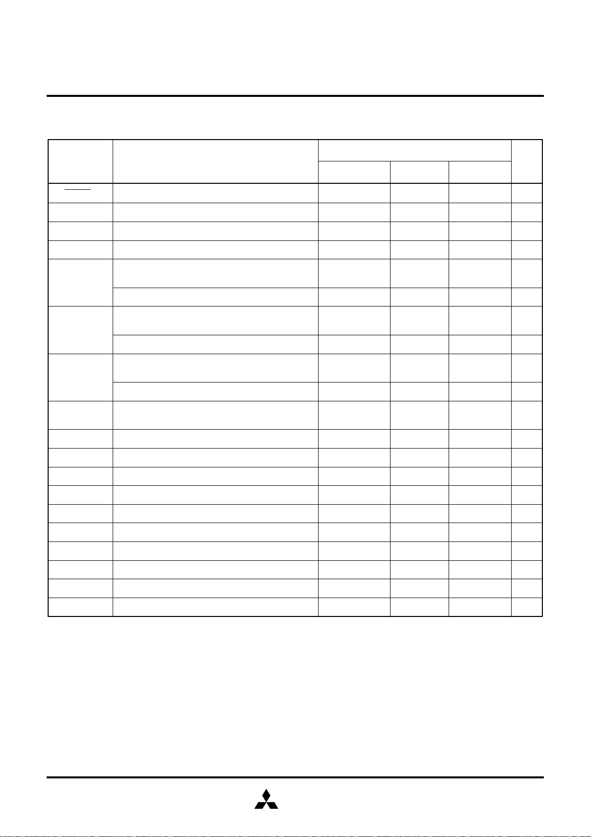
MITSUBISHI MICROCOMPUTERS
g
7630 Group
SINGLE-CHIP 8-BIT CMOS MICROCOMPUTER
Table 11: Timing requirements
Symbol Parameter
(RESET)
t
W
t
C(XIN
t
WH(XIN
t
WL(XIN
t
(CNTR)
C
(CNTR)
t
WH
(CNTR)
t
WL
)
)
)
Reset input “L” pulse width
External clock input cycle time 100 ns
External clock input “H” pulse width 37 ns
External clock input “L” pulse width 37 ns
, CNTR1 input cycle time
CNTR
0
(except bi-phase counter mode)
input cycle time (bi-phase counter mode)
CNTR
0
, CNTR1 input “H” pulse width
CNTR
0
(except bi-phase counter mode)
input “H” pulse width (bi-phase counter mode)
CNTR
0
, CNTR1 input “L” pulse width
CNTR
0
(except bi-phase counter mode)
input “L” pulse width (bi-phase counter mode)
CNTR
0
(VCC=4.0 to 5.5 V, VSS=AVSS=0 V, Ta=–40 to 85 °C unless otherwise noted)
Limits
Unit
min. typ. max.
2 µs
1600 ns
2000 ns
800 ns
1000 ns
800 ns
1000 ns
of CNTR0 and TX0 input edges
tL(CNTR0-TX0)
(TX0)TX
t
C
(TX0)TX
t
WH
t
(TX0)TX
WL
t
(INT) INT0, INT1 input “H” pulse width
WH
(INT) INT0, INT1 input “L” pulse width
t
WL
t
)
C(SCLK
t
t
t
t
)
WH(SCLK
)
WL(SCLK
SU(SIN–SCLK
H(SCLK–SIN
La
(bi-phase counter mode)
input cycle time (bi-phase counter mode)
0
input “H” pulse width (bi-phase counter mode)
0
input “L” pulse width (bi-phase counter mode)
0
Serial I/O clock input cycle time
Serial I/O clock input “H” pulse width
Serial I/O clock input “L” pulse width
)
Serial I/O input setup time 200 ns
)
Serial I/O input hold time 150 ns
500 ns
3200 ns
1600 ns
1600 ns
460 ns
460 ns
8·tC(XIN)
4·tC(XIN)
4·tC(XIN)
ns
ns
ns
MITSUBISHI
ELECTRIC
45

MITSUBISHI MICROCOMPUTERS
7630 Group
SINGLE-CHIP 8-BIT CMOS MICROCOMPUTER
Table 12: Switching characteristics
Symbol Parameter
t
t
t
t
t
t
t
) Serial I/O clock output “H” pulse width 0.5 · tC(S
WH(SCLK
) Serial I/O clock output “L” pulse width 0.5 · tC(S
WL(SCLK
D(SCLK–SOUT
V(SCLK–SOUT
)
R(SCLK
(CMOS)
R
(CMOS)
F
)
)
measurement output pin
Serial I/O output delay time 50 ns
Serial I/O output valid time 0 50 ns
Serial I/O clock output rise time 50 ns
CMOS output rise time 10 50 ns
CMOS output fall time 10 50 ns
100 pF
(VCC = 4.0 to 5.5 V, VSS = AVSS = 0 V, Ta = –40 to 85 °C, unless otherwise noted)
Limits
Unit
min. typ. max.
CLK
CLK
)–50
)–50
ns
ns
CMOS output
Fig. 49 Circuit for measuring output switching characteristics
46
MITSUBISHI
ELECTRIC
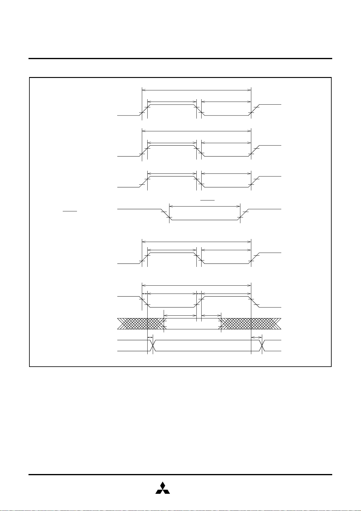
TIMING DIAGRAM
TX
0
CNTR0, CNTR
INT0, INT
1
MITSUBISHI MICROCOMPUTERS
7630 Group
SINGLE-CHIP 8-BIT CMOS MICROCOMPUTER
tC(TX0)
tWL(TX0)tWH(TX0)
0.8·V
CC
0.8·V
0.8·V
CC
CC
1
tC(CNTR)
0.2·V
0.2·V
0.2·V
CC
tWL(CNTR)tWH(CNTR)
CC
tWL(INT)tWH(INT)
CC
RESET
X
IN
S
CLK
S
IN
S
OUT
Fig. 50 Timing diagram
tWL(RESET)
0.2·V
CC
tC(XIN)
tWL(XIN)tWH(XIN)
0.8·V
CC
tWL(S
t
F
0.2·V
CC
tD(S
)t
CLK
tSU(SIN-S
CLK
0.8·V
CC
0.2·V
CC
)t
CLK-SOUT
t
C(SCLK
)
0.2·V
CC
)
t
R
0.8·V
CC
tH(S
CLK-SIN
WH(SCLK
)
)
(S
V
CLK-SOUT
)
MITSUBISHI
ELECTRIC
47

7630 English Data Sheets
REVISION DATE Page MODIFICATIONS
New Old
1.1 10. 98 “CAN controller” is replaced by “CAN module” in whole
document.
11 11 Schematics (8) and (11) are corrected.
18 18 Replaced: “PUPDj” with “PUP4j”
26 26 Replaced: “UTXD” with “SOUT”
Replaced: “URXD” with “SIN”
38 38 Replaced: “FFFBH” with “FFFB16”
Replaced: “FFFAH” with “FFFA16”
REVISION
41 Replaced: “44P6N” with “44P6N-A)
(1.2) 13.01.99 43 43 V alues changed:Iih(35, 113) to (20, 200) and Iil(-122, -70) to
(-200, -20); typical values are removed.
10 10 Schematic (1) is modified.
35 35 Fig. 39 is modified.
Revision Report M37630 E4/M4
1
 Loading...