

Mitsubishi M37560MF-XXXGP, M37560MF-XXXFP, M37560ME-XXXGP, M37560ME-XXXFP, M37560MD-XXXGP Datasheet
...
MITSUBISHI MICROCOMPUTERS
7560 Group
SINGLE-CHIP 8-BIT CMOS MICROCOMPUTER
DESCRIPTION
The 7560 group is the 8-bit microcomputer based on the 740 family core technology.
The 7560 group has the LCD drive control circuit, an 8-channel AD/D-A converter, UART and PWM as additional functions.
The various microcomputers in the 7560 group include variations
of internal memory size and packaging. For details, refer to the
section on part numbering.
For details on availability of microcomputers in the 7560 Group,
refer the section on group expansion.
FEATURES
Basic machine-language instructions....................................... 71
•
The minimum instruction execution time............................ 0.5 µs
•
Memory size
•
ROM ................................................................ 32 K to 6 0 K bytes
RAM ............................................................... 1024 to 2560 bytes
Programmable input/output ports ............................................. 55
•
Software pull-up resistors .................................................... Built-in
•
Output ports ................................................................................. 8
•
Input ports .................................................................................... 1
•
Interrupts .................................................. 17 sources, 16 vectors
•
(at 8 MHz oscillation frequency)
(includes key input interrupt)
Timers ........................................................... 8-bit ✕ 3, 16-bit ✕ 2
•
Serial I/O1 ..................... 8-bit ✕ 1 (UART or Clock-synchronous)
•
Serial I/O2 .................................... 8-bit ✕ 1 (Clock-synchronous)
•
PWM output .................................................................... 8-bit ✕ 1
•
A-D converter .................................................. 8-bit ✕ 8 channels
•
D-A converter .................................................. 8-bit ✕ 2 channels
•
LCD drive control circuit
•
Bias ................................................................................... 1/2, 1/3
Duty ............................................................................ 1/2, 1/3, 1/4
Common output .......................................................................... 4
Segment output......................................................................... 40
2 Clock generating circuits
•
(connect to external ceramic resonator or quartz-crystal oscillator)
Watchdog timer ............................................................. 14-bit ✕ 1
•
Power source voltage ................................................ 2.2 to 5.5 V
•
Power dissipation
•
In high-speed mode ...........................................................40 mW
(at 8 MHz oscillation frequency, at 5 V power source voltage)
In low-speed mode..............................................................6 0 µW
(at 32 kHz oscillation frequency, at 3 V power source voltage)
Operating temperature range ...................................– 20 to 85°C
•
APPLICATIONS
Camera, household appliances, consumer electronics, etc.
PIN CONFIGURATION (TOP VIEW)
0
1
2
3
4
5
1
1
1
1
1
G
G
G
G
G
S
S
E
S
E
S
E
E
S
E
1
7
6
4
5
L
N
N
N
N
V
/
/
/
/
7
6
5
4
6
6
6
6
P
P
P
P
A
A
A
A
A
L K 2
S E G
S E G
S E G
S E G
S E G
S E G
S E G
S E G
S E G
S E G
V
A V
C O M
C O M
C O M
C O M
V
R E F
V
V
1
G
S
E
E
8 1
9
8 2
8
8 3
7
8 4
6
8 5
5
8 6
4
8 7
3
8 8
2
8 9
1
9 0
0
9 1
C C
9 2
9 3
S S
9 4
3
9 5
2
9 6
1
9 7
0
9 8
L 3
9 9
L 2
10 0
C
2
1 234567891 01 11 21 314151617181 9202 122232425262 72 82 93 0
1
C
9
8
0
1
2
3
5
6
7
8
1
1
G
G
6
7
1
1
/
/
G
G
1
0
3
3
S E
S E
S E
P
S
S
E
P
4
2
2
2
2
2
2
2
2
2
G
G
G
G
G
G
G
G
/
/
/
/
2
3
4
5
3
3
3
3
S E
S E
S E
S E
P
P
P
P
G
/
/
/
/
/
6
7
0
1
2
3
0
0
3
0
S E
S E
S E
S E
S E
P
P
P
P
P
M37560MF-XXXFP
2
1
1
0
1
0
2
3
N
N
/
/
1
2
C
C
S
S
/
/
2
3
6
6
A
U T
P
P
A
L K 2
1
0
A
A
N
N
R
R
/
/
/
2
2
6
5
I
/
/
P
D
5
4
S
O
/
/
R T
5
5
0
S
7
/
P
P
6
C N T
C N T
5
1
P
A
N
6
P
A D T / D
P
1
1
0
P
P
M
M
R
S
/
/
/
3
2
/
/
7
0
1
5
5
4
5
5
P
P
R T
L K
P
D Y
P
P
P W
P W
9
0
1
2
4
5
6
7
8
3
2
3
3
3
3
3
G
G
G
G
G
G
/
/
/
/
/
/
3
4
5
6
7
0
0
0
0
0
0
S E
P
1
C
S
/
6
4
P
1
S E
S E
S E
S E
P
P
P
S E
P
P
2
1
T
D
D
T
T
X
X
O
T
R
/
T
/
/
/
5
4
2
1
4
4
/φ/
4
4
3
P
P
P
P
I N
I N
4
U
P
9
3
3
3
3
3
G
G
G
G
G
/
/
/
/
/
1
2
3
4
5
1
1
1
1
1
S E
S E
S E
P
P
P
S E
P
P
51525 35 45 55 65 7585 96 06 162636 46 56 66 76 86 97 0717 27 37 47 57 67 77 87 98 0
5 0
P 1
4 9
4 8
4 7
46
4 5
4 4
4 3
4 2
4 1
4 0
3 9
3 8
3 7
3 6
3 5
3 4
3 3
3 2
3 1
6
0
7
5
4
4
7
7
7
7
P
P
P
P
P
6
P 1
7
P 2
0
P 2
1
P 2
2
P2
3
P 2
4
P2
5
P 2
6
P 2
7
V
SS
X
OUT
X
IN
X
COUT
X
CIN
R E S E T
P 70/ I N T
P 7
1
P 7
2
P 7
3
0
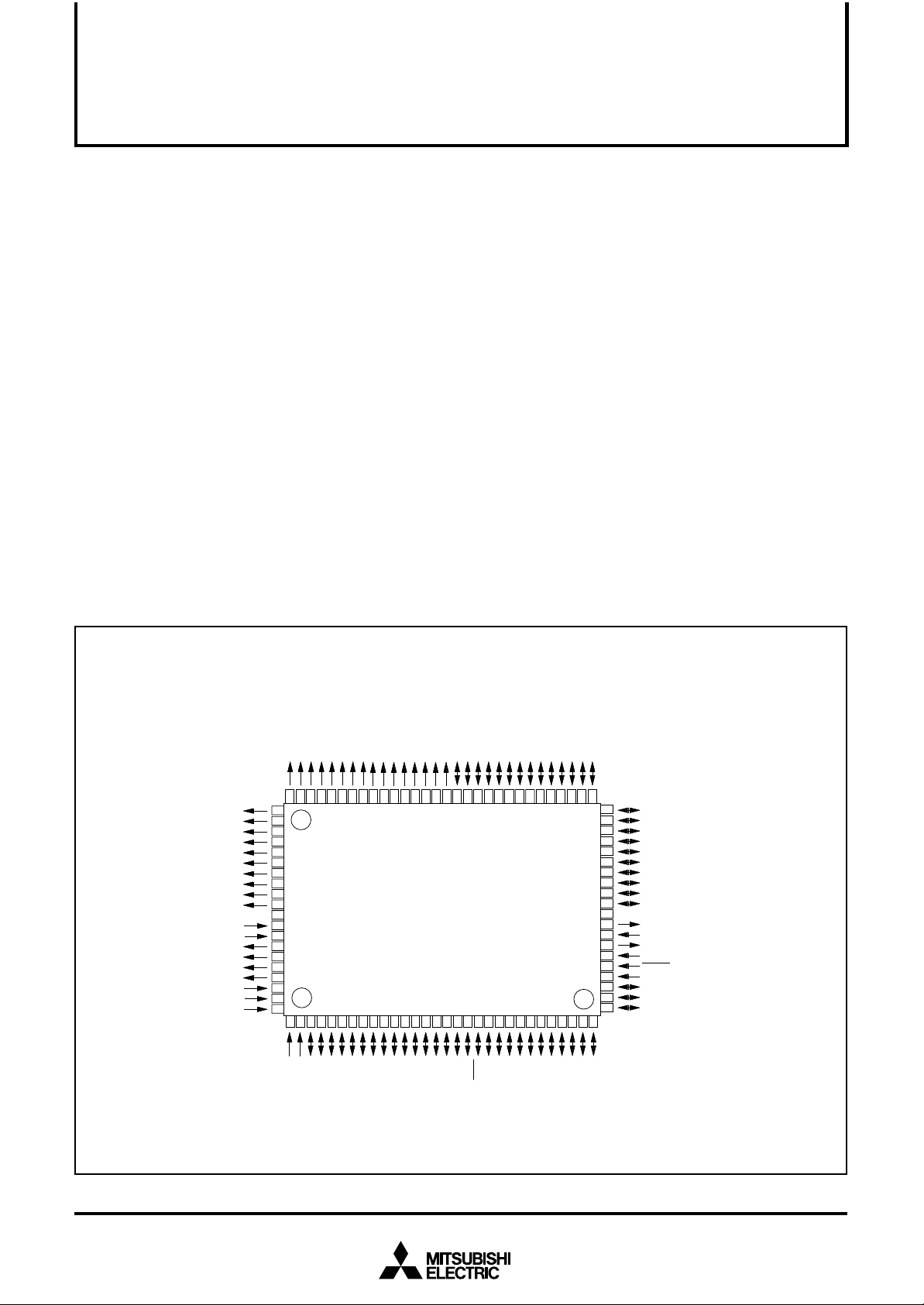
Package type : 100P6S-A
Fig. 1 Pin configuration of M37560MF-XXXFP
PIN CONFIGURATION (TOP VIEW)
3
4
5
6
1
1
1
1
G
G
G
G
S
E
S
E
S
E
S
E
S E G
S E G
S E G
S E G
S E G
S E G
S E G
SEG
S E G
S E G
SEG
SEG
S E G
V
AV
C O M
C O M
COM
COM
V
REF
V
V
V
1 2
1 1
1 0
9
8
7
6
5
4
3
2
1
0
CC
SS
3
2
1
0
L 3
L2
C
2
C
1
L 1
76
77
78
79
80
81
82
83
84
85
86
87
88
89
90
91
92
93
94
95
96
97
98
99
0 01
1 2345678910111 21 31 41 51 61 71 81 92 02 12 22 32 42 5
9
8
0
1
2
4
5
1
1
G
G
7
1
/
/
G
1
0
3
3
S E
S E
S E
P
P
S
E
3
2
2
2
2
2
G
G
/
/
2
3
3
3
S E
S E
P
P
2
G
G
G
G
/
/
/
/
4
5
6
7
3
3
3
3
S E
S E
S E
P
P
P
P
M37560MF-
6
2
G
/
0
0
S E
S E
P
XXX
MITSUBISHI MICROCOMPUTERS
7560 Group
SINGLE-CHIP 8-BIT CMOS MICROCOMPUTER
8
9
0
1
3
4
7
2
2
2
3
G
/
1
0
S E
P
3
G
G
G
G
/
/
/
/
2
3
4
5
0
0
0
0
S E
S E
S E
S E
P
P
P
P
GP
5
2
3
G
/
6
0
S E
P
6
3
G
/
7
0
S E
P
7
3
3
3
3
G
G
G
G
/
/
/
/
0
1
2
3
1
1
1
1
S E
S E
S E
P
P
P
P
5 15253545556575859606 1626364656 66 76 86 97 07 17 27 37 47 5
5 0
4 9
4 8
4 7
4 6
45
4 4
4 3
42
41
4 0
3 9
3 8
3 7
3 6
35
3 4
33
3 2
31
30
29
2 8
2 7
2 6
P14/SEG
P15/SEG
P1
6
P1
7
P2
0
P2
1
P2
2
P2
3
P2
4
P2
5
P2
6
P2
7
V
SS
X
OUT
X
IN
X
COUT
X
CIN
RESET
P70/INT
P7
1
P7
2
P7
3
P7
4
P7
5
P7
6
38
39
0
7
6
5
N
N
N
/
/
/
6
5
7
6
6
6
A
A
A
A
P
P
P
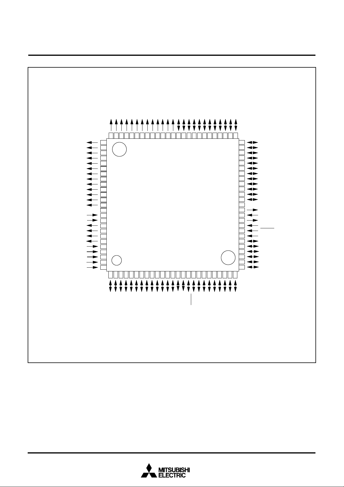
Package type : 100P6Q-A
Fig. 2 Pin configuration of M37560MF-XXXGP
4
2
3
N
N
N
/
/
/
4
1
2
6
P
C
C
S
S
/
/
2
3
6
6
A
U T
A
L K 2
A
P
P
L K 2
1
1
0
2
1
0
A
N
N
/
/
2
2
I
D
S
O
/
/
0
S
7
/
6
5
1
N
A
P
A D T / D
6
P
P
1
A
/
6
5
P
C N T
0
P
P
R
R
/
/
3
2
/
/
5
5
5
4
R T
R T
P
P
5
5
P W
C N T
P
P
1
1
0
1
D
D
X
M
/
1
5
P W
P
X
M
C
T
R
R
/
/
S
5
4
S
/
/
4
/
0
5
D Y
P
4
6
7
4
P
P
4
P
L K
P
U
0
7
1
2
T
4
7
T
T
P
P
O
/
/
T
1
2
4
4
/φ/
3
I N
I N
P
P
4
P
2
MITSUBISHI MICROCOMPUTERS
I
N
T
1
,
I
N
T
2
N
T
R
0
,
C
N
T
R
1
D
A
1
A
D
T
C
P
U
A
X
S
P
C
H
C
L
P
S
R
E S E
T
C
C
V
S
S
5
V
)
0
V
)
R O
M
A
M
5
9
1
0
P
4 ( 8 )P
2 ( 8
)
0 ( 8
)
P
1 ( 8
)
P
6 ( 8
)
P
7 ( 8
)
P
3 ( 8
)
P
5 ( 8
)
1
2
0
0
9
8
9
7
9
6
5
4
0
8
9
8
7
6
5
8
4
3
2
1
0
9
7
8
7
6
5
7
4
7
3
7
8
5
9
0
1
6
2
3
4
9
0
1
2
5
3
4
5
6
1
4
2
3
4
5
4
6
7
8
5
6
7
8
9
0
1
2
9
0
2
1
2
2
3
4
2
5
6
6
7
2
7
8
9
0
3
1
2
3
4
4
5
6
8
9
0
3
2
1
2
3
1
4
5
6
7
8
C
I
N
X
C
O U
T
X
N U
T
X
C
O U
T
X
I
N
I
/
O
1
(
8
)
V
R
E
F
A
V
S
S
L
1
1
2
L
2
V
L
3
C
O
M
0
C
O
M
1
C
O
M
2
C
O
M
3
E
G
0
E
G
1
E
G
2
S
E
G
3
S
E
G
4
S
E
G
5
S
E
G
6
S
E
G
7
S
E
G
8
S
E
G
9
E
G
1
0
E
G
1
1
E
G
1
2
E
G
1
3
E
G
1
4
S
E
G
1
5
S
E
G
1
6
S
E
G
1
7
φ
X
C
I
N
C
O U
T
X
3
8
9
S
I / O 2 ( 8
)
P
W M ( 8
)
φ
I
N
T
0
D
- A
2
-
A
1
A
2
T
O
U
T
L
C
D
d
r
i
v
e
c
o
n
t
r
o
l
c
i
r
c
u
i
t
L
C
D
d
i
s
p
l
a
y
R
A
M
(
2
0
b
y
t
e
s
)
T
i m e r X ( 1 6
)
T
i m e r Y ( 1 6
)
T
i m e r 1 ( 8
)
T
i m e r 2 ( 8
)
T
i m e r 3 ( 8
)
a
t
a
b
u
s
C
l
o
c
k
g
e
n
e
r
a
t
i
n
g
c
i
r
c
u
i
t
C
l o c
k
i
n p u
t
C
l o c
k
o
u t p u
t
u
b
-
c
l
o
c
k
u
t
p
u
t
S
u b - c l o c
k
i
n p u
t
e
s
e
t
K
e y i n p u t ( K e y - o n w a k e u p ) i n t e r r u p
t
R
e a l t i m e p o r t f u n c t i o
n
A
- D c o n v e r t e r ( 8
)
I
/ O p o r t P
0
I
/ O p o r t P
1
I
/
O
p
o
r
t
P
2
I
/ O p o r t P
4
I
/ O p o r t P
5
I
/
O
p
o
r
t
P
6
O
u
t
p
u
t
p
o
r
t
P
3
I
/
O
p
o
r
t
P
7
e
s
e
t
i
n
p
u
t
C
O
U
T
u
b
l
o
c
k
u
t
p
u
t
X C I
N
S
u b
c
l o c
k
i
n p u
t
W
a t c h d o g
t
i m e
r
7560 Group
SINGLE-CHIP 8-BIT CMOS MICROCOMPUTER
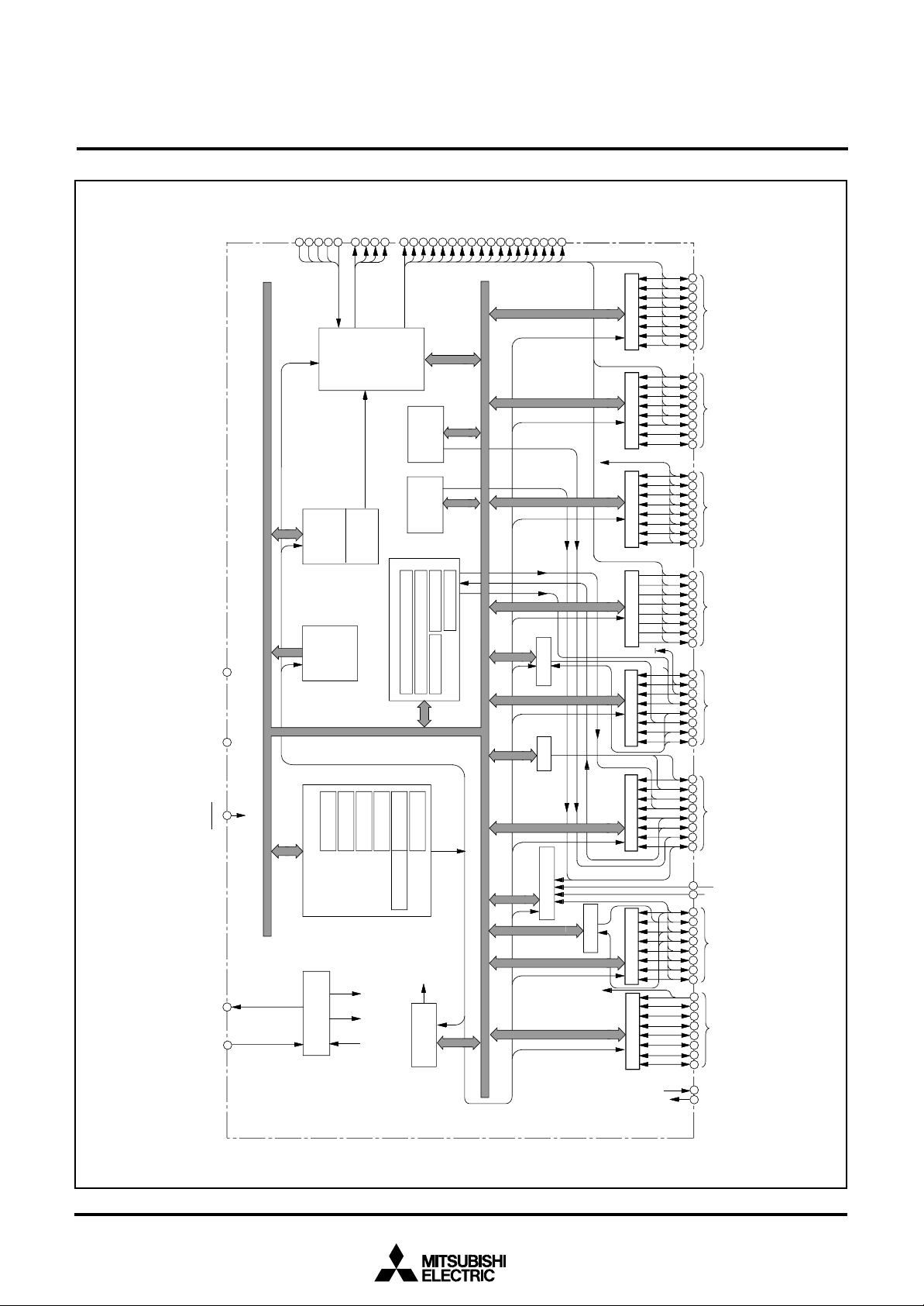
FUNCTIONAL BLOCK DIAGRAM (Package : 100P6S-A)
Fig. 3 Functional block diagram
3
PIN DESCRIPTION
Table 1 Pin description (1)
MITSUBISHI MICROCOMPUTERS
7560 Group
SINGLE-CHIP 8-BIT CMOS MICROCOMPUTER
V
CC, VSS
VREF
AVSS
RESET
XIN
XOUT
VL1–VL3
C1, C2
COM0–COM
SEG0–SEG
P00/SEG26–
P07/SEG33
P10/SEG34–
P15/SEG39
P16, P17
P20 – P27
P30/SEG18 –
P37/SEG
25
FunctionPin Name
Power source •Apply voltage of 2.2 V to 5.5 V to VCC, and 0 V to VSS.
Analog refer-
ence voltage
Analog power
source
Reset input
Clock input
Clock output
LCD power
source
Charge-pump
capacitor pin
Common output
3
17
Segment output
I/O port P0
I/O port P1
I/O port P2
Output port P3
•Reference voltage input pin for A-D converter.
•GND input pin for A-D converter.
•Connect to VSS.
•Reset input pin for active “L”.
•Input and output pins for the main clock generating circuit.
•Connect a ceramic resonator or a quartz-crystal oscillator between the XIN and XOUT pins to set
the oscillation frequency.
•If an external clock is used, connect the clock source to the XIN pin and leave the XOUT pin open. A
feedback resistor is built-in.
•Input 0 ≤ VL1 ≤ VL2 ≤ VL3 voltage.
•Input 0 – VL3 voltage to LCD. (0 ≤ VL1 ≤ VL2 ≤ VL3 when a voltage is multiplied.)
•External capacitor pins for a voltage multiplier (3 times) of LCD contorl.
•LCD common output pins.
•COM2 and COM3 are not used at 1/2 duty ratio.
•COM3 is not used at 1/3 duty ratio.
•LCD segment output pins.
•8-bit I/O port.
•CMOS compatible input level.
•CMOS 3-state output structure.
•Pull-up control is enabled.
•I/O direction register allows each 8-bit pin to be pro-
grammed as either input or output.
•6-bit I/O port with same function as port P0.
•CMOS compatible input level.
•CMOS 3-state output structure.
•Pull-up control is enabled.
•I/O direction register allows each 6-bit pin to be pro-
grammed as either input or output.
•2-bit I/O port.
•CMOS compatible input level.
•CMOS 3-state output structure.
•I/O direction register allows each pin to be individually programmred as either input or output.
•Pull-up control is enabled.
•8-bit I/O port with same function as P16 and P17.
•CMOS compatible input level.
•CMOS 3-state output structure.
•Pull-up control is enabled.
•8-bit output port with same function as port P0.
•CMOS 3-state output structure.
•Port output control is enabled.
Function except a port function
•LCD segment output pins
•Key input (key-on wake-up) interrupt
input pins
•LCD segment output pins
4
Table 2 Pin description (2)
MITSUBISHI MICROCOMPUTERS
7560 Group
SINGLE-CHIP 8-BIT CMOS MICROCOMPUTER
P40
P41/INT1,
P42/INT2
P43/φ/TOUT
P44/RXD,
P45/TXD,
P46/SCLK1,
P47/SRDY1
P50/PWM0,
P51/PWM1
P52/RTP0,
P53/RTP1
P54/CNTR0,
P55/CNTR1
P56/DA1,
P57/ADT/DA
P60/AN0/S
IN2,
P61/AN1/S
OUT2,
P62/AN2/S
CLK21,
P63/AN3/S
CLK22
P64/AN4–
P67/AN7
P70/INT0
P71–P77
XCOUT
XCIN
I/O port P4
I/O port P5
2
I/O port P6
Input port P7
I/O port P7
Sub-clock output
Sub-clock input
FunctionPin Name
•1-bit I/O port with same function as P16 and P17.
•CMOS compatible input level.
•N-channel open-drain output structure.
•7-bit I/O port with same function as P16 and P17.
•CMOS compatible input level.
•CMOS 3-state output structure.
•Pull-up control is enabled.
•8-bit I/O port with same function as P16 and P17.
•CMOS compatible input level.
•CMOS 3-state output structure.
•Pull-up control is enabled.
•8-bit I/O port with same function as P16 and P17.
•CMOS compatible input level.
•CMOS 3-state output structure.
•Pull-up control is enabled.
•1-bit input port.
•7-bit I/O port with same function as P16 and P17.
•CMOS compatible input level.
•N-channel open-drain output structure.
•Sub-clock generating circuit I/O pins.
(Connect a resonator. External clock cannot be used.)
Function except a port function
•Interrupt input pins
•φ clock output pin
•Timer 2 output pin
•Serial I/O1 I/O pins
•PWM function pins
•Real time port function pins
•Timer X, Y function pins
•D-A conversion output pins
•A-D conversion input pins
•Serial I/O2 I/O pins
•A-D conversion input pins
•Interrupt input pin
5
PART NUMBERING
M
M
X X X
F P
P
ROM/PROM si
b
The fi
ROM
M
Mask ROM
R O M
Pack
r o d u c
3 7 5 6 0
t
F –
MITSUBISHI MICROCOMPUTERS
7560 Group
SINGLE-CHIP 8-BIT CMOS MICROCOMPUTER
age type
FPGP: 100P6S-A pac kage
: 100P6Q-A package
n u m b e
1
: 4096
2
: 8192 byt es
3
: 12288 bytes
4
: 16384 bytes
5
: 20480 bytes
6
: 24576 bytes
7
: 28672 bytes
8
: 32768 bytes
9
: 36864 bytes
A
: 40960 bytes
B
: 45056 bytes
C
: 49152 bytes
D
: 53248 bytes
E
: 57344 bytes
F
: 61440 bytes
rst 128 bytes and the last 2 bytes of
are reser ved areas ; they cannot be used.
emory type
M :
r
ze
ytes
version
Fig. 4 Part numbering
6
MITSUBISHI MICROCOMPUTERS
7560 Group
SINGLE-CHIP 8-BIT CMOS MICROCOMPUTER
GROUP EXPANSION
Mitsubishi plans to expand the 7560 group as follows.
Memory Type
Support for mask ROM version.
Memory Size
ROM size ........................................................... 32 K to 60 K bytes
RAM size .......................................................... 1024 to 2560 bytes
Memory Expansion Plan
ROM size (bytes)
60K
56K
52K
4 8 K
4 4 K
4 0 K
3 6 K
32K
28K
24K
20K
16K
1 2 K
8 K
4K
Under development
M37560M8
Packages
100P6Q-A .................................. 0.5 mm-pitch plastic molded QFP
100P6S-A ................................ 0.65 mm-pitch plastic molded QFP
Under development
M 3 7 5 6 0 M F
2 5 65
Fig. 5 Memory expansion plan
Currently products are listed below.
Table 3. List of products
Product
M37560M8-XXXFP
M37560M8-XXXGP
M37560MF-XXXFP
M37560MF-XXXGP
ROM size (bytes)
ROM size for User in ( )
32768
(32638)
61440
(61310)
1
27 6 81
0 2
RAM size (bytes)
1024
2560
41 2 8 01 5 3 61 7 9 2192 2 0 4 8 2304 2560
RAM size (bytes)
Package
100P6S-A
100P6Q-A
100P6S-A
100P6Q-A
Mask ROM version
Mask ROM version
Mask ROM version
Mask ROM version
Remarks
As of Mar. 2001
7
MITSUBISHI MICROCOMPUTERS
7560 Group
SINGLE-CHIP 8-BIT CMOS MICROCOMPUTER
FUNCTIONAL DESCRIPTION
CENTRAL PROCESSING UNIT (CPU)
The 7560 group uses the standard 740 family instruction set. Refer to the table of 740 family addressing modes and machine
instructions or the 740 Family Software Manual for details on the
instruction set.
Machine-resident 740 family instructions are as follows:
The FST and SLW instruction cannot be used.
The STP, WIT, MUL, and DIV instruction can be used.
[Accumulator (A)]
The accumulator is an 8-bit register. Data operations such as data
transfer, etc., are executed mainly through the accumulator.
[Index Register X (X)]
The index register X is an 8-bit register. In the index addressing
modes, the value of the OPERAND is added to the contents of
register X and specifies the real address.
[Index Register Y (Y)]
The index register Y is an 8-bit register. In partial instruction, the
value of the OPERAND is added to the contents of register Y and
specifies the real address.
[Stack Pointer (S)]
The stack pointer is an 8-bit register used during subroutine calls
and interrupts. This register indicates start address of stored area
(stack) for storing registers during subroutine calls and interrupts.
The low-order 8 bits of the stack address are determined by the
contents of the stack pointer. The high-order 8 bits of the stack
address are determined by the stack page selection bit. If the
stack page selection bit is “0” , the high-order 8 bits becomes
“0016”. If the stack page selection bit is “1”, the high-order 8 bits
becomes “0116”.
The operations of pushing register contents onto the stack and
popping them from the stack are shown in Figure 7.
Store registers other than those described in Figure 7 with program when the user needs them during interrupts or subroutine
calls.
[Program Counter (PC)]
The program counter is a 16-bit counter consisting of two 8-bit
registers PCH and PCL. It is used to indicate the address of the
next instruction to be executed.
b7
b0
A Accumulator
b7
b0
X Index register X
b7
b0
Y Index register Y
b7 b0
S Stack pointer
b7b15 b0
H
PC
L
Program counterPC
b7 b0
N V T B D I Z C Processor status register (PS)
Carry flag
Zero flag
Interrupt disable flag
Decimal mode flag
Break flag
Index X mode flag
Overflow flag
Negative flag
Fig. 6 740 Family CPU register structure
8
On-going Routin
e
MITSUBISHI MICROCOMPUTERS
7560 Group
SINGLE-CHIP 8-BIT CMOS MICROCOMPUTER
P u s h r e t u r n a d d r e s s
o n s t a c k
P O P re t u r n
a d d r e s s f r o m s t a c k
I n t e r r u p t r e q u e s t
M ( S )( P CH)
(S)
M ( S )( P CL)
( S )
S u b r o u t i n e
E x e c u t e R T S
( S )
( P CL)M ( S )
(S)
( P CH)M ( S )
(S) – 1
( S ) – 1
( S ) + 1
(S) + 1
( N o t e )
Execute JSR
M (S) (PCH)
(S) – 1
(S)
M ( S )( P CL)
( S )
( S ) – 1
M (S) (PS)
( S )
( S ) – 1
I n t e r r u p t
S e r v i c e R o u t i n e
E x e c u t e R T I
(S)
(S) + 1
( P S )M ( S )
(S)
(S) + 1
( P CL)M ( S )
(S)
(S) + 1
P u s h r e t u r n a d d r e s s
o n s t a c k
P u s h c o n t e n t s o f p r o c e s s o r
s t a t u s r e g i s t e r o n s t a c k
I F l a g i s s e t f r o m “ 0 ” t o “ 1 ”
F e t c h t h e j u m p v e c t o r
POP contents of
processor status
register from stack
P O P r e t u r n
a d d r e s s
f r o m s t a c k
(PCH)M (S)
N o t e: C o n d i t i o n f o r a c c e p t a n c e o f a n i n t e r r u p t I n t e r r u p t e n a b l e f l a g i s “ 1 ”
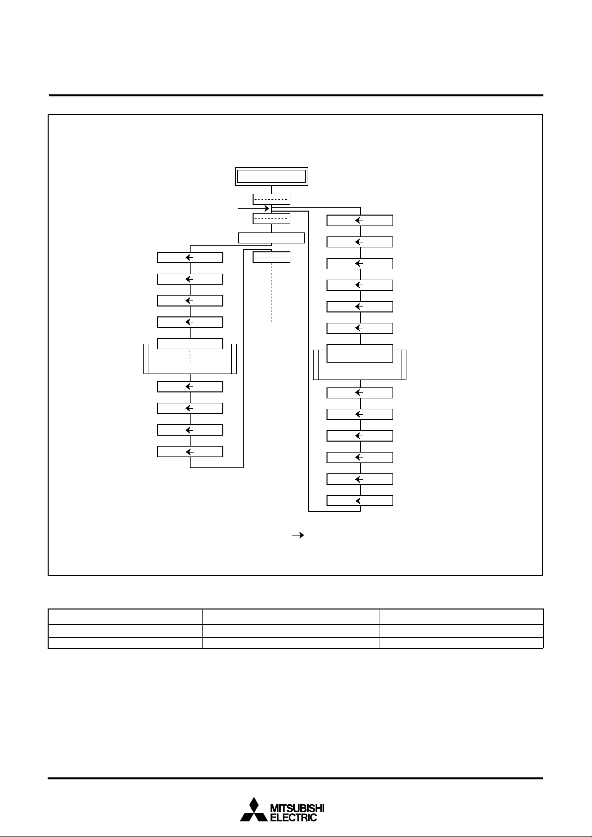
Fig. 7 Register push and pop at interrupt generation and subroutine call
Table 4 Push and pop instructions of accumulator or processor status register
Push instruction to stack
Accumulator
Processor status register
Interrupt disable flag is “0”
PHA
PHP
Pop instruction from stack
PLA
PLP
9
MITSUBISHI MICROCOMPUTERS
7560 Group
SINGLE-CHIP 8-BIT CMOS MICROCOMPUTER
[Processor status register (PS)]
The processor status register is an 8-bit register consisting of 5
flags which indicate the status of the processor after an arithmetic
operation and 3 flags which decide MCU operation. Branch operations can be performed by testing the Carry (C) flag , Zero (Z) flag,
Overflow (V) flag, or the Negative (N) flag. In decimal mode, the Z,
V, N flags are not valid.
• Bit 0: Carry flag (C)
The C flag contains a carry or borrow generated by the arithmetic logic unit (ALU) immediately after an arithmetic operation.
It can also be changed by a shift or rotate instruction.
• Bit 1: Zero flag (Z)
The Z flag is set if the result of an immediate arithmetic operation
or a data transfer is “0”, and cleared if the result is anything other
than “0”.
• Bit 2: Interrupt disable flag (I)
The I flag disables all interrupts except for the interrupt generated by the BRK instruction.
Interrupts are disabled when the I flag is “1”.
• Bit 3: Decimal mode flag (D)
The D flag determines whether additions and subtractions are
executed in binary or decimal. Binary arithmetic is executed
when this flag is “0”; decimal arithmetic is executed when it is
“1”.
Decimal correction is automatic in decimal mode. Only the ADC
and SBC instructions can be used for decimal aritmetic.
• Bit 4: Break flag (B)
The B flag is used to indicate that the current interrupt was generated by the BRK instruction. The BRK flag in the processor
status register is always “0”. When the BRK instruction is used to
generate an interrupt, the processor status register is pushed
onto the stack with the break flag set to “1”.
• Bit 5: Index X mode flag (T)
When the T flag is “0”, arithmetic operations are performed between accumulator and memory. When the T flag is “1”, direct
arithmetic operations and direct data transfers are enabled between memory locations.
• Bit 6: Overflow flag (V)
The V flag is used during the addition or subtraction of one byte
of signed data. It is set if the result exceeds +127 to -128. When
the BIT instruction is executed, bit 6 of the memory location operated on by the BIT instruction is stored in the overflow flag.
• Bit 7: Negative flag (N)
The N flag is set if the result of an arithmetic operation or data
transfer is negative. When the BIT instruction is executed, bit 7
of the memory location operated on by the BIT instruction is
stored in the negative flag.
Table 5 Set and clear instructions of each bit of processor status register
Set instruction
Clear instruction
C flag
SEC
CLC
Z flag
–
–
I flag
SEI
CLI
D flag
SED
CLD
B flag
–
–
T flag
SET
CLT
V flag
–
CLV
N flag
–
–
10
[CPU Mode Register (CPUM)] 003B16
N
P
CPU
( C P U M
B
)
b
b
The CPU mode register contains the stack page selection bit and
the internal system clock selection bit.
The CPU mode register is allocated at address 003B16.
MITSUBISHI MICROCOMPUTERS
7560 Group
SINGLE-CHIP 8-BIT CMOS MICROCOMPUTER
7
Fig. 8 Structure of CPU mode register
0
mode register
( C M ) : a d d r e s s 0 0 3
rocessor mode bits
b1 b0
0 0 : Single-chip mode
0 1 :
1 0 :
1 1 :
Stack page selection bit
0 : 0 page
1 : 1 page
Not used (returns “1” when read)
(Do not write “0” to this bit)
Port X
0 : Oscillation stop
1 : X
Main clock (X
0 : Oscillating
1 : Stopped
Main clock division ratio selection bit
0 : f(X
1 : f(XIN)/8 (middle-s peed mode)
Internal system clock selection bit
0 : X
1 : XCIN–XCOUT selected ( low-speed m ode)
ot available
C switch bit
CIN–XCOUT oscillating function
IN–XOUT) stop bit
IN)/2 (high-speed m ode)
IN–XOUT selected (m iddle-/high-speed mode)
1 6
11
MITSUBISHI MICROCOMPUTERS
FF
RAM
RAM si
Add
6
2
8
4
0
6
2
8
4
0
6
2
8
4
0
F
F
ROM
ROM si
Add
Add
F F
FFDC
FFFE
FFFF
XXXX
YYYY
ZZZZ
RAM
R O M
R
SFR
N
)
I
a
R
ROM
Z
S
LCD displ
RAM
R
ROM
N
RAM
7560 Group
SINGLE-CHIP 8-BIT CMOS MICROCOMPUTER
MEMORY
Special Function Register (SFR) Area
The Special Function Register area in the zero page contains control registers such as I/O ports and timers.
RAM
RAM is used for data storage and for stack area of subroutine
calls and interrupts.
ROM
The first 128 bytes and the last 2 bytes of ROM are reserved for
device testing and the rest is user area for storing programs.
Interrupt Vector Area
The interrupt vector area contains reset and interrupt vectors.
area
ze
(bytes)
1 9 2
2 5 6
3 8 4
5 1 2
6 4 0
7 6 8
8 9 6
1 0 2 4
1 5 3 6
2 0 4 8
2 5 6 0
ress
XXXX
00
013F
01BF
023F
02BF
033F
03BF
043F
063F
083F
0A3F
16
16
16
16
16
16
16
16
16
16
16
16
Zero Page
The 256 bytes from addresses 000016 to 00FF16 are called the
zero page area. The internal RAM and the special function registers (SFR) are allocated to this area.
The zero page addressing mode can be used to specify memory
and register addresses in the zero page area. Access to this area
with only 2 bytes is possible in the zero page addressing mode.
Special Page
The 256 bytes from addresses FF0016 to FFFF16 are called the
special page area. The special page addressing mode can be
used to specify memory addresses in the special page area. Access to this area with only 2 bytes is possible in the special page
addressing mode.
0 0 0 0
1 6
0040
0054
0 1 0 0
0440
area
16
16
1 6
16
ay
area
eserved area
16
e r o p a g
e
area
ze
(bytes)
409
819
1228
1638
2048
2457
2867
3276
3686
4096
4505
4915
5324
5734
6144
ote: When
area exceeds 1024 bytes, the areas shown the table are us ed.
Fig. 9 Memory map diagram
12
YYYY
000
E000
D000
C000
B000
A000
9000
8000
7000
6000
5000
4000
3000
2000
1000
ress
ot used (Note
16
16
16
16
16
16
16
16
16
16
16
16
16
16
16
16
ZZZZ
080
E080
D080
C080
B080
A080
9080
8080
7080
6080
5080
4080
3080
2080
1080
16
16
16
16
16
16
16
16
16
16
16
16
16
16
16
16
ress
16
eserved
area
(128 by tes)
16
0
1 6
0
16
16
16
nterrupt vector are
eserved
area
p e c i a l p a g
e
MITSUBISHI MICROCOMPUTERS
A
B
C
D
E
F
A
B
C
D
E
F
A
B
C
D
E
F
A
B
C
D
E
F
P
)
P
)
P
)
P
)
P
)
P
)
P
)
P
)
P
)
P
D)
P
)
P
)
P
)
P
)
Serial I/O
(SIO1STS)
Serial I/O
(SIO1CON)
UART
(UARTCON)
B
)
I
)
T i
)
Ti
(TXM)
( I N T E D G E )
CPU
(CPUM)
I
)
I
)
I
)
T i
)
T i
)
T i
)
T i
)
T i
)
Ti
(high) (TYH)
PULL
(PULLA)
P U L L
)
Ti
(TYM)
Ti
M)
T
(CKOUT)
S
(SEG)
L C D
)
A-D
(ADCON)
A-D
(AD)
T
(TB/RB)
R
K
(KIC)
P
)
P
)
R
Serial I/O
(SIO2CON)
S
)
PWM
(PWMCON)
P W M
)
P W M
)
R
R
R
R
D-A
(DA1)
D-A
(DA2)
D
A
l
)
7560 Group
SINGLE-CHIP 8-BIT CMOS MICROCOMPUTER
0 0 0 0
0001
0002
0 0 0 3
0 0 0 4
0 0 0 5
0 0 0 6
0 0 0 7
0 0 0 8
0 0 0 9
000
000
0 0 0
0 0 0
0 0 0
000
0010
0 0 1 1
0 0 1 2
0 0 1 3
0014
0015
0016
0017
0 0 1 8
0 0 1 9
001
001
001
001
001
0 0 1
o r t P 0 ( P 0
1 6
o r t P 0 d i r e c t i o n r e g i s t e r ( P 0 D
16
16
ort P1 (P1
o r t P 1 d i r e c t i o n r e g i s t e r ( P 1 D
1 6
o r t P 2 ( P 2
1 6
o r t P 2 d i r e c t i o n r e g i s t e r ( P 2 D
1 6
o r t P 3 ( P 3
1 6
o r t P 3 o u t p u t c o n t r o l r e g i s t e r ( P 3 C
1 6
o r t P 4 ( P 4
1 6
o r t P 4 d i r e c t i o n r e g i s t e r ( P 4 D
1 6
16
ort P5 (P5
16
ort P5 direction register (P5
o r t P 6 ( P 6
1 6
o r t P 6 d i r e c t i o n r e g i s t e r ( P 6 D
1 6
o r t P 7 ( P 7
1 6
o r t P 7 d i r e c t i o n r e g i s t e r ( P 7 D
16
16
1 6
1 6
1 6
e s e r v e d a r e
16
16
ey input control register
16
r e g i s t e r B ( P U L L B
16
1 6
ransmit/Receive buffer register
1 6
16
16
a u d r a t e g e n e r a t o r ( B R G
16
16
e s e r v e d a r e
16
e r i a l I / O 2 r e g i s t e r ( S I O 2
1 6
a
register A
1 status register
1 control register
control register
2 control register
a
m e r X ( l o w ) ( T X L
0 0 2 0
1 6
m e r X ( h i g h ) ( T X H
0021
16
m e r Y ( l o w ) ( T Y L
0022
16
0 0 2 3
1 6
mer Y
m e r 1 ( T 1
0 0 2 4
1 6
m e r 2 ( T 2
0 0 2 5
1 6
m e r 3 ( T 3
0 0 2 6
1 6
0 0 2 7
1 6
0 0 2 8
0 0 2 9
002
002
0 0 2
0 0 2
002
002
0030
0 0 3 1
0 0 3 2
0 0 3 3
0034
0035
0036
0037
0 0 3 8
0 0 3 9
003
003
003
003
003
003
mer X mode register
1 6
mer Y mode register
1 6
mer 12 3 mode register (T123
16
OUT
/φ output cont rol register
16
control register
p r e s c a l e r ( P R E P W M
1 6
r e g i s t e r ( P W M
1 6
e s e r v e d a r e
16
e s e r v e d a r e
16
e s e r v e d a r e
16
1 6
eserved area
1 6
1 6
16
16
-
r e g i s t e r ( D A C O N
16
16
W a t c h d o g t i m e r c o n t r o l r e g i s t e r ( W D T C O N )
1 6
egment output enable register
m o d e r e g i s t e r ( L M
1 6
16
I n t e r r u p t e d g e s e l e c t i o n r e g i s t e r
16
n t e r r u p t r e q u e s t r e g i s t e r 1 ( I R E Q 1
16
n t e r r u p t r e q u e s t r e g i s t e r 2 ( I R E Q 2
16
n t e r r u p t c o n t r o l r e g i s t e r 1 ( I C O N 1
16
n t e r r u p t c o n t r o l r e g i s t e r 2 ( I C O N 2
16
a
a
a
1 conversion register
2 conversion register
control register
conversion register
c o n t r o
mode register
Fig. 10 Memory map of special function register (SFR)
13
MITSUBISHI MICROCOMPUTERS
P
P U L L
A
b
b
P
D i
PULL
B
b
b
N
PULL
PULL
7560 Group
SINGLE-CHIP 8-BIT CMOS MICROCOMPUTER
I/O PORTS
Direction Registers
The I/O ports (ports P0, P1, P2, P4, P5, P6, P71–P77) have direction registers which determine the input/output direction of each
individual pin. (Ports P00–P07 are shared with bit 0 of the port P0
direction register, and ports P10–P15 shared with bit 0 of the port
P1 direction register.) Each bit in a direction register corresponds
to one pin, and each pin can be set to be input port or output port.
When “0” is written to the bit corresponding to a pin, that pin becomes an input pin. When “1” is written to that bit, that pin becomes an output pin.
If data is read from a pin set to output, the value of the port output
latch is read, not the value of the pin itself. Pins set to input are
floating. If a pin set to input is written to, only the port output latch
is written to and the pin remains floating.
Port P3 Output Control Register
Bit 0 of the port P3 output control register (address 000716) enables control of the output of ports P30–P37.
When the bit is set to “1”, the port output function is valid.
When resetting, bit 0 of the port P3 output control register is set to
“0” (the port output function is invalid) and pulled up.
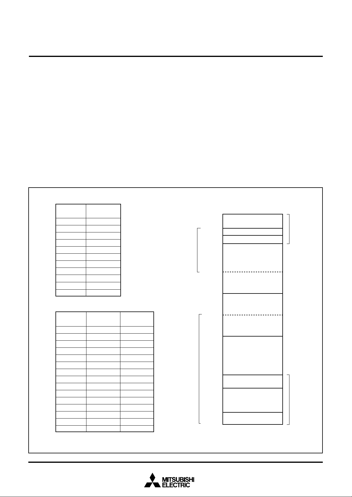
Pull-up Control
By setting the PULL register A (address 001616) or the PULL register B (address 001716), ports P0 to P2, P4 to P6 can control pullup with a program.
However, the contents of PULL register A and PULL register B do
not affect ports programmed as the output ports.
The PULL register A setting is invalid for pins set to segment output with the segment output enable register.
7
7
ote:The contents of
do not affect ports programmed as the output port.
0
r e g i s t e r
( P U L L A : a d d r e s s 0 0 1 61
00, P01 pull-up
P0
2, P03 pull-up
P0
4–P07 pull-up
P1
0–P13 pull-up
P1
4, P15 pull-up
P1
6, P17 pull-up
P2
0–P23 pull-up
P2
4–P27 pull-up
0
register
(PULLB : addr ess 001716)
41–P43 pull-up
P4
4–P47 pull-up
P5
0–P53 pull-up
P5
4–P57 pull-up
P6
0–P63 pull-up
P6
4–P67 pull-up
Not used (return “0” when read)
register A and
6)
s a b l
0 :
1 : E n a b l e
register B
e
Fig. 11 Structure of PULL register A and PULL register B
14
Table 6 List of I/O port function (1)
Pin
P00/SEG26–
P07/SEG33
P10/SEG34–
P15/SEG39
P16 , P17
P20–P27
P30/SEG18–
P37/SEG25
Port P0
Port P1
Port P2
Port P3
Input/OutputName
Input/output,
byte unit
Input/output,
6-bit unit
Input/output,
individual bits
Input/output,
individual bits
Output
I/O Format
CMOS compatible
input level
CMOS 3-state output
CMOS compatible
input level
CMOS 3-state output
CMOS compatible
input level
CMOS 3-state output
CMOS compatible
input level
CMOS 3-state output
CMOS 3-state output
SINGLE-CHIP 8-BIT CMOS MICROCOMPUTER
Non-Port Function
LCD segment output
LCD segment output
Key input (key-on
wake-up) interrupt
input
LCD segment output
MITSUBISHI MICROCOMPUTERS
7560 Group
Related SFRs
PULL register A
Segment output enable
register
PULL register A
Segment output enable
register
PULL register A
PULL register A
Interrupt control register2
Key input control register
Segment output enable
register
P3 output enable register
Diagram No.
(1)
(2)
(1)
(2)
(4)
(3)
P40
P41/INT1,
P42/INT2
P43/φ/TOUT
P44/RXD,
P45/TXD,
P46/SCLK1,
P47/SRDY1
P50/PWM0,
P51/PWM1
P52/RTP0,
P53/RTP1
P54/CNTR0
P55/CNTR1
P56/DA1
P57/ADT/
DA2
Port P4
Port P5
Input/output,
individual bits
Input/output,
individual bits
CMOS compatible
input level
N-channel open-drain
output
CMOS compatible
input level
CMOS 3-state output
CMOS compatible
input level
CMOS 3-state output
External interrupt input
Timer output
φ output
Serial I/O1 function I/O
PWM output
Real time port
function output
Timer X function I/O
Timer Y function input
DA1 output
DA2 output
A-D trigger input
Interrupt edge selection
register
PULL register B
Timer 123 mode register
TOUT/φ output control
register
PULL register B
Serial I/O1 control register
Serial I/O1 status register
UART control register
PULL register B
PWM control register
PULL register B
Timer X mode register
PULL register B
Timer X mode register
PULL register B
Timer Y mode register
PULL register B
D-A control register
PULL register B
D-A control register
A-D control register
(13)
(4)
(12)
(5)
(6)
(7)
(8)
(10)
(9)
(11)
(14)
(15)
(15)
15
MITSUBISHI MICROCOMPUTERS
SINGLE-CHIP 8-BIT CMOS MICROCOMPUTER
Table 7 List of I/O port function (2)
Pin Name I/O Format Non-Port Function Related SFRS
P60/SIN2/AN0
P61/SOUT2/
AN1
P62/SCLK21/
AN2
P63/SCLK22 /
AN3
P64/AN4–
P67/AN7
P70/INT0
P71–P77
Port P6
Port P7
Input/Output
Input/
output,
individual
bits
Input
Input/
output,
individual
bits
CMOS compatible input
level
CMOS 3-state output
CMOS compatible input
level
CMOS compatible input
level
N-channel open-drain
output
A-D conversion input
Serial I/O2 function I/O
A-D conversion input
External interrupt input
PULL register B
A-D control register
Serial I/O2 control
register
A-D control register
PULL register B
Interrupt edge
selection register
7560 Group
Diagram No.
(17)
(18)
(19)
(20)
(16)
(23)
(13)
COM0–COM3
SEG0–SEG17
Notes1: How to use double-function ports as function I/O ports, refer to the applicable sections.
2: Make sure that the input level at each pin is either 0 V or V
tential, a current will flow V
Common
Segment
Output
Output
CC to VSS through the input-stage gate.
LCD common output
LCD segment output
CC during execution of the STP instruction. When an input level is at an intermediate po-
LCD mode register
(21)
(22)
16
MITSUBISHI MICROCOMPUTERS
7560 Group
SINGLE-CHIP 8-BIT CMOS MICROCOMPUTER
( 1 ) P o r t s P 01– P 07, P 11– P 1
S e g m e n t d a t a
D a t a b u s
(2) Ports P00, P1
D a t a b u sP
P o r t l a t c h
P o r t d i r e c t i o n r e g i s t e r
0
D i r e c t i o n r e g i s t e r
S e g m e n t d a t a
o r t l a t c
h
( 3 ) P o r t P 3
Segment data
D a t a b u s
Port latch
5
L C D d r i v e t i m i n g
I n t e r f a c e l o g i c l e v e l
s h i f t c i r c u i t
P o r t / S e g m e n t
LCD drive timing
Port/Segment
LCD drive timing
I n t e r f a c e l o g i c l e v e l
s h i f t c i r c u i t
Port/Segment
Port direction register
Interface logic level
shift circuit
Port direction register
Output control
P u l l - u p
VL2/VL3/V
S e g m e n t / P o r t
S e g m e n t
V
L 1
/ V
P o r t
VL2/VL3/V
S e g m e n t / P o r t
Segment
Pull-up
V
L 2
/ V
L 3
/ V
Segment/Port
S e g m e n t
VL1/V
P o r t
CC
S S
Pull-up
Port
C C
SS
VL1/V
CC
SS
( 4 ) P o r t s P 16, P 17, P 2 , P 41, P 4
D i r e c t i o n
r e g i s t e r
D a t a b u s
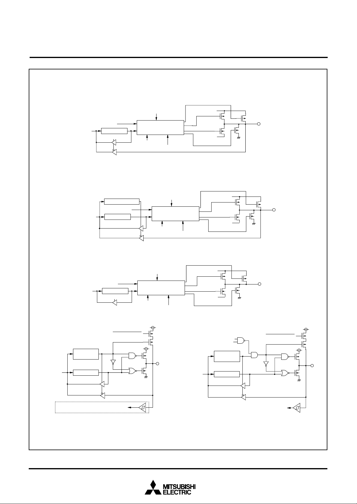
Fig. 12 Port block diagram (1)
Port latch
Key-on wake up interrupt input
1
, INT2 interrupt input
INT
2
E x c e p t P 1
Pull-up control
6
, P 1
7
(5) Port P4
S e r i a l I / O 1 e n a b l e b i t
R e c e p t i o n e n a b l e b i t
Data bus
4
D i r e c t i o n
r e g i s t e r
Port latch
P u l l - u p c o n t r o l
S e r i a l I / O 1 i n p u t
17
MITSUBISHI MICROCOMPUTERS
7560 Group
SINGLE-CHIP 8-BIT CMOS MICROCOMPUTER
( 6 ) P o r t P 4
5
P 4
D a t a b u s
( 8 ) P o r t P 4
S e r i a l I / O 1 m o d e s e l e c t i o n b i t
Data bus
5
/ T x D P - c h a n n e l o u t p u t d i s a b l e b i t
S e r i a l I / O 1 e n a b l e b i t
T r a n s m i s s i o n e n a b l e b i t
S
D i r e c t i o n
r e g i s t e r
P o r t l a t c h
S e r i a l I / O 1 o u t p u t
7
S e r i a l I / O 1 e n a b l e b i t
R D Y 1
o u t p u t e n a b l e b i t
D i r e c t i o n
r e g i s t e r
Port latch
P u l l - u p c o n t r o l
P u l l - u p c o n t r o l
( 7 ) P o r t P 4
Serial I/O1 synchronization
clock selection bit
S e r i a l I / O 1 e n a b l e b i t
Serial I/O1 mode selection bit
Data bus
( 9 ) P o r t s P 52, P 5
Data bus
6
Serial I/O1 enable bit
Serial I/O1 clock output
D i r e c t i o n
r e g i s t e r
P o r t l a t c h
3
D i r e c t i o n
r e g i s t e r
Port latch
P u l l - u p c o n t r o l
S e r i a l I / O 1 c l o c k i n p u t
Pull-up control
Serial I/O1 ready output
(10) Ports P50,P5
Data bus
P W M f u n c t i o n e n a b l e b i t
P W M o u t p u t
1
Direction
register
Port latch
P u l l - u p c o n t r o l
Real time control bit
Real time port data
( 1 1 ) P o r t P 5
D a t a b u s
Pulse output mode
4
D i r e c t i o n
r e g i s t e r
P o r t l a t c h
Timer output
Pull-up control
CNTR0 interrupt input
Fig. 13 Port block diagram (2)
18
MITSUBISHI MICROCOMPUTERS
7560 Group
SINGLE-CHIP 8-BIT CMOS MICROCOMPUTER
( 1 2 ) P o r t P 4
T
OUT
/φ output control
T
O U T
/φ s e l e c t i o n b i t
( 1 4 ) P o r t P 5
Data bus
3
D i r e c t i o n
r e g i s t e r
P o r t l a t c hD a t a b u s
Timer output
φ o u t p u t
5
Direction
register
P o r t l a t c h
P u l l - u p c o n t r o l
P u l l - u p c o n t r o l
( 1 3 ) P o r t s P 40, P 71– P 7
Direction
register
P o r t l a t c hData bus
(15) Ports P56,P5
D a t a b u s
7
D i r e c t i o n
r e g i s t e r
Port latch
7
P u l l - u p c o n t r o l
C N T R1 i n t e r r u p t i n p u t
( 1 6 ) P o r t s P 64– P 6
Data bus
7
D i r e c t i o n
r e g i s t e r
P o r t l a t c h
A - D c o n v e r s i o n i n p u t
Fig. 14 Port block diagram (3)
Pull-up control
Analog input pin selection bit
(17) Port P6
Data bus
E x c e p t P 5
0
Port latch
6
D - A c o n v e r t e r o u t p u t
D i r e c t i o n
r e g i s t e r
A-D conversion input
A - D t r i g g e r i n p u t
D-A
Pull-up control
S e r i a l I / O 2 i n p u t
Analog input pin selection bit
1
,D-A2 output enable bit
19
MITSUBISHI MICROCOMPUTERS
t
t
7560 Group
SINGLE-CHIP 8-BIT CMOS MICROCOMPUTER
( 1 8 ) P o r t P 6
P61/S
OUT2
S e r i a l I / O 2 t r a n s m i t e n d s i g n a l
S y n c h r o n o u s c l o c k s e l e c t i o n b i
S e r i a l I / O 2 p o r t s e l e c t i o n b i
( 2 0 ) P o r t P 6
Synchronous clock selection bit
Synchronous clock output pin selection bit
1
P-channel output disable bit
D i r e c t i o n
r e g i s t e r
Port latchD a t a b u s
S e r i a l I / O 2 o u t p u t
3
Serial I/O2 port selection bit
A - D c o n v e r s i o n i n p u t
Direction
register
P o r t l a t c hD a t a b u s
Pull-up control
Synchronous clock output pin
Analog input pin selection bit
Pull-up control
(19) Port P6
S y n c h r o n o u s c l o c k s e l e c t i o n b i t
Serial I/O2 port selection bit
2
selection bit
D i r e c t i o n
r e g i s t e r
Port latchD a t a b u s
S e r i a l I / O 2 c l o c k o u t p u t
(21)COM0–COM
V
L 3
V
L 2
V
L1
Pull-up control
S e r i a l I / O 2 c l o c k i n p u t
A-D conversion input
Analog input pin selection bit
3
The gate input signal of each
transistor is controlled by the LCD
duty ratio and the bias value.
S e r i a l I / O 2 c l o c k o u t p u t
( 2 2 ) S E G0– S E G
VL2/V
V
L 1
/ V
S S
1 7
L3
Fig. 15 Port block diagram (4)
A-D conversion input
Analog input pin selection bit
T h e v o l t a g e a p p l i e d t o t h e s o u r c e s o f P c h a n n e l a n d N - c h a n n e l t r a n s i s t o r s i s t h e
c o n t r o l l e d v o l t a g e b y t h e b i a s v a l u e .
( 2 3 ) P o r t P 7
Data bus
0
V
SS
Direction
register
Port latch
I N T0 i n p u t
20

MITSUBISHI MICROCOMPUTERS
7560 Group
SINGLE-CHIP 8-BIT CMOS MICROCOMPUTER
INTERRUPTS
Interrupts occur by seventeen sources: seven external, nine inter-
nal, and one software.
Interrupt Control
Each interrupt is controlled by an interrupt request bit, an interrupt
enable bit, and the interrupt disable flag except for the software interrupt set by the BRK instruction. An interrupt occurs if the corresponding interrupt request and enable bits are “1” and the interrupt disable flag is “0”.
Interrupt enable bits can be set or cleared by software.
Interrupt request bits can be cleared by software, but cannot be
set by software.
The BRK instruction cannot be disabled with any flag or bit. The I
flag disables all interrupts except the BRK instruction interrupt.
When several interrupts occur at the same time, the interrupts are
received according to priority.
Table 8 Interrupt vector addresses and priority
Interrupt Source
Reset (Note 2)
INT0
INT1
Serial I/O1
reception
Serial I/O1
transmission
Timer X
Timer Y
Timer 2
Timer 3
CNTR0
CNTR1
Timer 1
INT2
Serial I/O2
Key input
(Key-on wake-up)
ADT
A-D conversion
Priority
1
2
3
4
5
6
7
8
9
10
11
12
13
14
15
16
Vector Addresses (Note 1)
LowHigh
FFFD16
FFFB16
FFF916
FFF716
FFF516
FFF316
FFF116
FFEF16
FFED16
FFEB16
FFE916
FFE716
FFE516
FFE316
FFE116
FFDF16
FFFC16
FFFA16
FFF816
FFF616
FFF416
FFF216
FFF016
FFEE16
FFEC16
FFEA16
FFE816
FFE616
FFE416
FFE216
FFE016
FFDE16
Interrupt Operation
By acceptance of an interrupt, the following operations are automatically performed:
1. The contents of the program counter and the processor status
register are automatically pushed onto the stack.
2. The interrupt disable flag is set and the corresponding interrupt
request bit is cleared.
3. The interrupt jump destination address is read from the vector
table into the program counter.
Interrupt Request
Generating Conditions
At reset
At detection of either rising or
falling edge of INT0 input
At detection of either rising or
falling edge of INT1 input
At completion of serial I/O1 data
reception
At completion of serial I/O1
transmit shift or when transmission buffer is empty
At timer X underflow
At timer Y underflow
At timer 2 underflow
At timer 3 underflow
At detection of either rising or
falling edge of CNTR0 input
At detection of either rising or
falling edge of CNTR1 input
At timer 1 underflow
At detection of either rising or
falling edge of INT2 input
At completion of serial I/O2 data
transmission or reception
At falling of conjunction of input
level for port P2 (at input mode)
At falling edge of ADT input
At completion of A-D conversion
Non-maskable
External interrupt
(active edge selectable)
External interrupt
(active edge selectable)
Valid when serial I/O1 is selected
Valid when serial I/O1 is selected
External interrupt
(active edge selectable)
External interrupt
(active edge selectable)
External interrupt
(active edge selectable)
Valid when serial I/O2 is selected
External interrupt
(valid at falling)
Valid when ADT interrupt is selected
External interrupt
(valid at falling)
Valid when A-D interrupt is selected
Remarks
BRK instruction
Notes1: Vector addresses contain interrupt jump destination addresses.
2: Reset function in the same way as an interrupt with the highest priority.
17
FFDD16
FFDC16
At BRK instruction execution
Non-maskable software interrupt
21
MITSUBISHI MICROCOMPUTERS
t
t
t
b7b
I
I N T
i
(INTEDGE
A16)
I
I N T
i
I
INT
d
(IREQ
C16)
(ICON
E16)
I
C N T R
i
( I R E Q
D
)
I
CNTR
I
d
(ICON
F16)
lli
b
b
b
b
b
b
b7b
7560 Group
SINGLE-CHIP 8-BIT CMOS MICROCOMPUTER
■Notes on interrupts
When setting the followings, the interrupt request bit may be set to
“1”.
•When setting external interrupt active edge
Related register: Interrupt edge selection register (address 3A16)
Timer X mode register (address 2716)
Timer Y mode register (address 2816)
•When switching interrupt sources of an interrupt vector address
where two or more interrupt sources are allocated
Related register: Interrupt source selection bit of A-D control
regsiter (bit 6 of address 3416)
Interrupt request bi
Interrupt enable bi
Interrupt disable flag (I)
BRK instruction
Fig. 16 Interrupt control
0
n t e r r u p t e d g e s e l e c t i o n r e g i s t e
: address 003
n t e r r u p t e d g e s e l e c t i o n b i
0
I N T1 i n t e r r u p t e d g e s e l e c t i o n b i t
I N T
2
i n t e r r u p t e d g e s e l e c t i o n b i t
N o t u s e d ( r e t u r n “ 0 ” w h e n r e a d )
r
t
0 : Fa
1 : Rising edge ac ti ve
When not requiring for the interrupt occurrence synchronous with
these setting, take the following sequence.
➀Set the corresponding interrupt enable bit to “0” (disabled).
➁Set the interrupt edge select bit (polarity switch bit) or the inter-
rupt source select bit to “1”.
➂Set the corresponding interrupt request bit to “0” after 1 or more
instructions have been executed.
➃Set the corresponding interrupt enable bit to “1” (enabled).
Rese
ng edge active
I n t e r r u p t r e q u e s t
7
7
Fig. 17 Structure of interrupt-related registers
0
n t e r r u p t r e q u e s t r e g i s t e r
1 : address 003
n t e r r u p t r e q u e s t b i
0
I N T1 i n t e r r u p t r e q u e s t b i t
S e r i a l I / O 1 r e c e i v e i n t e r r u p t r e q u e s t b i t
S e r i a l I / O 1 t r a n s m i t i n t e r r u p t r e q u e s t b i t
T i m e r X i n t e r r u p t r e q u e s t b i t
T i m e r Y i n t e r r u p t r e q u e s t b i t
T i m e r 2 i n t e r r u p t r e q u e s t b i t
T i m e r 3 i n t e r r u p t r e q u e s t b i t
0
n t e r r u p t c o n t r o l r e g i s t e r
1 : address 003
0
interrupt enable bit
INT
1
interrupt enable bit
Serial I/O1 receive interrupt enable bit
Serial I/O1 transmit interrupt enable bit
Timer X interrupt enable bit
Timer Y inter rup t ena bl e bi t
Timer 2 inter ru pt enable bit
Timer 3 inter ru pt enable bit
1
t
1
7
0
nterrupt request register 2
2 : a d d r e s s 0 0 3
n t e r r u p t r e q u e s t b i
0
C N T R
1
i n t e r r u p t r e q u e s t b i t
T i m e r 1 i n t e r r u p t r e q u e s t b i t
I N T
2
i n t e r r u p t r e q u e s t b i t
S e r i a l I / O 2 i n t e r r u p t r e q u e s t b i t
K e y i n p u t i n t e r r u p t r e q u e s t b i t
A D T / A D c o n v e r s i o n i n t e r r u p t r e q u e s t b i t
N o t u s e d ( r e t u r n s “ 0 ” w h e n r e a d )
0 : No interrupt re quest issue
1 : Interrupt request issued
0
n t e r r u p t c o n t r o l r e g i s t e r
2 : address 003
0
interrupt enable bit
CNTR
1
interrupt enable bit
Timer 1 interrupt enable bit
INT
2
interrupt enable bit
Serial I/O2 interrupt enable bit
Key input interrupt enable bit
ADT/AD conversion interrupt enable bit
Not used (returns “0” when read)
(Do not write “1” to this bit)
n t e r r u p t s d i s a b l e
0 :
1 : I n t e r r u p t s e n a b l e d
1 6
t
2
22

MITSUBISHI MICROCOMPUTERS
A
”
7560 Group
SINGLE-CHIP 8-BIT CMOS MICROCOMPUTER
Key Input Interrupt (Key-on Wake Up)
A Key-on wake up interrupt request is generated by applying “L”
level voltage to any pin of port P2 that have been set to input
mode. In other words, it is generated when AND of input level
P o r t P X x
“ L ” l e v e l o u t p u t
o u t p u
P 2
o u t p u
P 2
P2
7
6
5 output
P U L L r e g i s t e r
B i t 2 = “ 1
✽✽
t
✽✽
t
✽✽
P o r t P 2
7
d i r e c t i o n r e g i s t e r = “ 1 ”
✽
Port P2
direction register = “1”
✽
Port P2
direction register = “1”
✽
Key input control register = “1”
7
P o r t P 2
l a t c h
K e y i n p u t c o n t r o l r e g i s t e r = “ 1 ”
6
6
Port P2
latch
K e y i n p u t c o n t r o l r e g i s t e r = “ 1 ”
5
5
Port P2
latch
goes from “1” to “0”. An example of using a key input interrupt is
shown in Figure 18, where an interrupt request is generated by
pressing one of the keys consisted as an active-low key matrix
which inputs to ports P20–P23.
Key input interrupt request
P2
4 output
i n p u
P 2
P2
i n p u
P 2
i n p u
P 2
3
2 input
1
0
✽✽
✽✽ ✽
t
✽✽
✽✽ ✽
t
✽✽
t
P o r t P 2
d i r e c t i o n r e g i s t e r = “ 1 ”
✽
P o r t P 2
d i r e c t i o n r e g i s t e r = “ 0 ”
Port P22
direction register = “0”
✽
P o r t P 2
d i r e c t i o n r e g i s t e r = “ 0 ”
P o r t P 2
d i r e c t i o n r e g i s t e r = “ 0 ”
✽
K e y i n p u t c o n t r o l r e g i s t e r = “ 1 ”
4
4
Port P2
latch
K e y i n p u t c o n t r o l r e g i s t e r = “ 1 ”
3
P o r t P 2
3
l a t c h
K e y i n p u t c o n t r o l r e g i s t e r = “ 1 ”
2
Port P2
latch
K e y i n p u t c o n t r o l r e g i s t e r = “ 1 ”
1
P o r t P 2
1
l a t c h
0
K e y i n p u t c o n t r o l r e g i s t e r = “ 1 ”
P o r t P 20
l a t c h
Port P2
Input reading circuit
✽ P - c h a n n e l t r a n s i s t o r f o r p u l l - u p
✽ ✽ C M O S o u t p u t b u f f e r
Fig. 18 Connection example when using key input control register, key input interrupt and port P2 block diagram
23

MITSUBISHI MICROCOMPUTERS
7560 Group
SINGLE-CHIP 8-BIT CMOS MICROCOMPUTER
TIMERS
The 7560 group has five timers: timer X, timer Y, timer 1, timer 2,
and timer 3. Timer X and timer Y are 16-bit timers, and timer 1,
timer 2, and timer 3 are 8-bit timers.
All timers are down count timers. When the timer reaches “0016”,
an underflow occurs at the next count pulse and the corresponding timer latch is reloaded into the timer and the count is continued. When a timer underflows, the interrupt request bit corresponding to that timer is set to “1”.
R e a l t i m e p o r t
P 52/ R T P
P 53/ R T P
P54/CNTR
P 5
P 55/ C N T R
3
/φ/ T
P 4
0
1
f(X
(f(X
0
Pulse width
measurement
mode
4
d i r e c t i o n r e g i s t e r
C N T R
e d g e s w i t c h b i t
1
I N
) / 1 6
f ( X
( f ( X
C I N
) / 1 6 w h e n φ = X
O U T
P 4
3
d i r e c t i o n r e g i s t e r
c o n t r o l b i t “ 1 ”
“ 0 ”
R e a l t i m e p o r t
c o n t r o l b i t “ 1 ”
“ 0 ”
IN
)/16
CIN
)/16 when φ = X
C N T R0 a c t i v e
e d g e s w i t c h b i t
“0”
“1”
CNTR
edge switch bit
P u l s e o u t p u t m o d e
1
a c t i v e
“ 0 ”
“ 1 ”
C I N
T i m e r 1 c o u n t s o u r c e
s e l e c t i o n b i t
X
CIN
T
OUT
output
control bit
Q D
L a t c h
Q D
L a t c h
CIN
T i m e r X o p e r a t i n g m o d e b i t s
“ 0 0 ” , “ 0 1 ” , “ 1 1 ”
"10"
0
active
4
latch
P5
f ( X
I N
) / 1 6
( f ( X
C I N
) / 1 6 w h e n φ = X
" 0 0 " , " 0 1 " , " 1 1 "
Timer Y
"10"
operating
mode bits
/ 2 )
“0”
“ 1 ”
T
O U T
o u t p u t
a c t i v e e d g e
s w i t c h b i t “ 0 ”
P 4
3
l a t c h
/2)
T i m e r 1 l a t c h ( 8 )
“ 0 ”
“1”
Timer 1 (8)
T
OUT
control bit
Q
“ 1 ”
Q
f ( X
I N
) / 1 6
( f ( X
C I N
w h e n φ = X
P 52 d a t a f o r
r e a l t i m e p o r t
P5
3
data for
real time port
Real time port
control bit “0”
“ 1 ”
T i m e r X s t o p
c o n t r o l b i t
T i m e r X ( l o w ) l a t c h ( 8 )
Timer X (low) (8)
P u l s e o u t p u t m o d e
S
Q
T
Q
Rising edge detection
Falling edge detection
C I N
/ 2 )
Timer Y stop
control bit
Timer Y (low) latch (8) T i m e r Y ( h i g h ) l a t c h ( 8 )
Timer Y (low) (8) Timer Y (high) (8)
T i m e r 2 c o u n t s o u r c e
s e l e c t i o n b i t
“ 0 ”
“1”
f(X
IN
)/16
(f(X
CIN
output
S
T
“ 0 ”
) / 1 6
C I N
/ 2 )
“1”
T i m e r 3 c o u n t
s o u r c e s e l e c t i o n b i t
Read and write operation on 16-bit timer must be performed for
both high- and low-order bytes. When reading a 16-bit timer, read
the high-order byte first. When writing to a 16-bit timer, write the
low-order byte first. The 16-bit timer cannot perform the correct
operation when reading during the write operation, or when writing
during the read operation.
Data bus
Timer X mode register
write signal
Timer X write
control bit
Timer X (high) latch (8)
Pulse width HL continuous ly
measurement mode
Period
measurement mode
T i m e r 2 l a t c h ( 8 )
Timer 2 (8)
)/16 when φ = X
CIN
Timer 3 latch (8)
Timer 3 (8)
Timer X (high) (8)
/2)
T i m e r 2 w r i t e
c o n t r o l b i t
T i m e r X
i n t e r r u p t
r e q u e s t
T i m e r Y
i n t e r r u p t
r e q u e s t
T i m e r 1
i n t e r r u p t
r e q u e s t
Timer 2
interrupt
request
T i m e r 3
i n t e r r u p t
r e q u e s t
Fig. 19 Timer block diagram
24

Timer X
Ti
T i
b
b
Timer X is a 16-bit timer that can be selected in one of four modes
and can be controlled the timer X write and the real time port by
setting the timer X mode register.
(1) Timer mode
The timer counts f(XIN)/16 (or f(XCIN)/16 in low-speed mode).
(2) Pulse output mode
Each time the timer underflows, a signal output from the CNTR0
pin is inverted. Except for this, the operation in pulse output mode
is the same as in timer mode. When using a timer in this mode,
set the corresponding port P54 direction register to output mode.
(3) Event counter mode
The timer counts signals input through the CNTR0 pin.
Except for this, the operation in event counter mode is the same
as in timer mode. When using a timer in this mode, set the corresponding port P54 direction register to input mode.
(4) Pulse width measurement mode
The count source is f(XIN)/16 (or f(XCIN)/16 in low-speed mode). If
CNTR0 active edge switch bit is “0”, the timer counts while the input signal of CNTR0 pin is at “H”. If it is “1”, the timer counts while
the input signal of CNTR0 pin is at “L”. When using a timer in this
mode, set the corresponding port P54 direction register to input
mode.
MITSUBISHI MICROCOMPUTERS
7560 Group
SINGLE-CHIP 8-BIT CMOS MICROCOMPUTER
7
Fig. 20 Structure of timer X mode register
0
mer X mode register
(TXM : address 0027
m e r X w r i t e c o n t r o l b i
0 : W r i t e v a l u e i n l a t c h a n d c o u n t e r
1 : W r i t e v a l u e i n l a t c h o n l y
R e a l t i m e p o r t c o n t r o l b i t
0 : R e a l t i m e p o r t f u n c t i o n i n v a l i d
1 : R e a l t i m e p o r t f u n c t i o n v a l i d
2
d a t a f o r r e a l t i m e p o r t
P 5
3
d a t a f o r r e a l t i m e p o r t
P 5
T i m e r X o p e r a t i n g m o d e b i t s
b 5 b 4
00 : T i m e r m o d e
01 : P u l s e o u t p u t m o d e
10 : E v e n t c o u n t e r m o d e
11 : P u l s e w i d t h m e a s u r e m e n t m o d e
0
a c t i v e e d g e s w i t c h b i t
C N T R
0 : C o u n t a t r i s i n g e d g e i n e v e n t c o u n t e r m o d e
S t a r t f r o m “ H ” o u t p u t i n p u l s e o u t p u t m o d e
M e a s u r e “ H ” p u l s e w i d t h i n p u l s e w i d t h m e a s u r e m e n t
m o d e
F a l l i n g e d g e a c t i v e f o r C N T R
1 : C o u n t a t f a l l i n g e d g e i n e v e n t c o u n t e r m o d e
S t a r t f r o m “ L ” o u t p u t i n p u l s e o u t p u t m o d e
M e a s u r e “ L ” p u l s e w i d t h i n p u l s e w i d t h m e a s u r e m e n t
m o d e
R i s i n g e d g e a c t i v e f o r C N T R
T i m e r X s t o p c o n t r o l b i t
0 : C o u n t s t a r t
1 : C o u n t s t o p
16
)
t
0
i n t e r r u p t
0
i n t e r r u p t
●Timer X Write Control
If the timer X write control bit is “0”, when the value is written in the
address of timer X, the value is loaded in the timer X and the latch
at the same time.
If the timer X write control bit is “1”, when the value is written in the
address of timer X, the value is loaded only in the latch. The value
in the latch is loaded in timer X after timer X underflows.
If the value is written in latch only, unexpected value may be set in
the high-order counter when the writing in high-order latch and the
underflow of timer X are performed at the same timing.
●Real Time Port Control
While the real time port function is valid, data for the real time port
are output from ports P52 and P53 each time the timer X
underflows. (However, if the real time port control bit is changed
from “0” to “1” after set of the real time port data, data are output
independent of the timer X operation.) If the data for the real time
port is changed while the real time port function is valid, the
changed data are output at the next underflow of timer X.
Before using this function, set the corresponding port direction
registers to output mode.
■Note on CNTR0 interrupt active edge selection
CNTR0 interrupt active edge depends on the CNTR0 active edge
switch bit.
25
MITSUBISHI MICROCOMPUTERS
T i
b
b
7560 Group
SINGLE-CHIP 8-BIT CMOS MICROCOMPUTER
Timer Y
Timer Y is a 16-bit timer that can be selected in one of four modes.
(1) Timer mode
The timer counts f(XIN)/16 (or f(XCIN)/16 in low-speed mode).
(2) Period measurement mode
CNTR1 interrupt request is generated at rising/falling edge of
CNTR1 pin input signal. Simultaneously, the value in timer Y latch
is reloaded in timer Y and timer Y continues counting down. Except for the above-mentioned, the operation in period measurement mode is the same as in timer mode.
The timer value just before the reloading at rising/falling of CNTR1
pin input signal is retained until the timer Y is read once after the
reload.
The rising/falling timing of CNTR1 pin input signal is found by
CNTR1 interrupt. When using a timer in this mode, set the corresponding port P55 direction register to input mode.
(3) Event counter mode
The timer counts signals input through the CNTR1 pin.
Except for this, the operation in event counter mode is the same
as in timer mode. When using a timer in this mode, set the corresponding port P55 direction register to input mode.
(4) Pulse width HL continuously measure-
ment mode
CNTR1 interrupt request is generated at both rising and falling
edges of CNTR1 pin input signal. Except for this, the operation in
pulse width HL continuously measurement mode is the same as in
period measurement mode. When using a timer in this mode, set
the corresponding port P55 direction register to input mode.
7
0
m e r Y m o d e r e g i s t e
( T Y M : a d d r e s s 0 0 2 8
Not used (return “0” when read)
Timer Y opera ti ng mo de bits
b5 b4
0 0 : Timer mode
0 1 : Period measurement mode
1 0 : Event counter mode
1 1 : Pulse width HL continuously
measurement mode
1
active edge sw itch bi t
CNTR
0 : Count at rising edge in event counter mode
Measur e the fal l i ng edg e to f all in g edg e
period in period measurement mode
Falling edge activ e f or CNTR
1 : Count at falling edge in event counter mode
Measure the rising edge period in period
measurement mode
Rising edge active for CNTR
Time r Y st o p co ntrol bi t
0 : Count start
1 : Count stop
r
1 6
Fig. 21 Structure of timer Y mode register
)
1
interrupt
1
interrupt
■Note on CNTR1 interrupt active edge selection
CNTR1 interrupt active edge depends on the CNTR1 active edge
switch bit. However, in pulse width HL continuously measurement
mode, CNTR1 interrupt request is generated at both rising and
falling edges of CNTR1 pin input signal regardless of the setting of
CNTR1 active edge switch bit.
26

Timer 1, Timer 2, Timer 3
T
i
T i
N
f(X
)
b
b
Timer 1, timer 2, and timer 3 are 8-bit timers. The count source for
each timer can be selected by timer 123 mode register. The timer
latch value is not affected by a change of the count source. However, because changing the count source may cause an inadvertent count down of the timer. Therefore, rewrite the value of timer
whenever the count source is changed.
●Timer 2 Write Control
If the timer 2 write control bit is “0”, when the value is written in the
address of timer 2, the value is loaded in the timer 2 and the latch
at the same time.
If the timer 2 write control bit is “1”, when the value is written in the
address of timer 2, the value is loaded only in the latch. The value
in the latch is loaded in timer 2 after timer 2 underflows.
●Timer 2 Output Control
When the timer 2 (TOUT) is output enabled, an inversion signal
from pin TOUT is output each time timer 2 underflows.
In this case, set the port P56 shared with the port TOUT to the output mode.
■Note on Timer 1 to Timer 3
When the count source of timers 1 to 3 is changed, the timer
counting value may be changed large because a thin pulse is generated in count input of timer. If timer 1 output is selected as the
count source of timer 2 or timer 3, when timer 1 is written, the
counting value of timer 2 or timer 3 may be changed large because a thin pulse is generated in timer 1 output.
Therefore, set the value of timer in the order of timer 1, timer 2
and timer 3 after the count source selection of timer 1 to 3.
MITSUBISHI MICROCOMPUTERS
7560 Group
SINGLE-CHIP 8-BIT CMOS MICROCOMPUTER
7
ote: Internal clock φ is
Fig. 22 Structure of timer 123 mode register
0
m e r 1 2 3 m o d e r e g i s t e
( T 1 2 3 M : a d d r e s s 0 0 2 9
v e e d g e s w i t c h b i
O U T
o u t p u t a c t
0 : S t a r t a t “ H ” o u t p u t
1 : S t a r t a t “ L ” o u t p u t
O U T
/φ o u t p u t c o n t r o l b i t
T
0 : T
O U T
/φ o u t p u t d i s a b l e d
O U T
/φ o u t p u t e n a b l e d
1 : T
T i m e r 2 w r i t e c o n t r o l b i t
0 : W r i t e d a t a i n l a t c h a n d c o u n t e r
1 : W r i t e d a t a i n l a t c h o n l y
T i m e r 2 c o u n t s o u r c e s e l e c t i o n b i t
0 : T i m e r 1 o u t p u t
I N
) / 1 6
1 : f ( X
C I N
) / 1 6 i n l o w - s p e e d m o d e )
( o r f ( X
T i m e r 3 c o u n t s o u r c e s e l e c t i o n b i t
0 : T i m e r 1 o u t p u t
I N
) / 1 6
1 : f ( X
C I N
) / 1 6 i n l o w - s p e e d m o d e )
( o r f ( X
T i m e r 1 c o u n t s o u r c e s e l e c t i o n b i t
I N
) / 1 6
0 : f ( X
C I N
) / 1 6 i n l o w - s p e e d m o d e )
( o r f ( X
C I N
)
1 : f ( X
N o t u s e d ( r e t u r n “ 0 ” w h e n r e a d )
CIN
/2 in the low-speed mode.
r
1 6
)
t
27

MITSUBISHI MICROCOMPUTERS
P
S
P
S
P
RXD
P
TXD
X
F/F
Add
R
(RBF)
R
)
S h i f
k
S
A d d
C
BRG
D
A d d
Shif
k
T
hif
hif
(TSC)
T
(TBE)
T
)
T
Add
D
A d d
A
R
S
D
D0D1D2D3D4D5D
RBF
TBE
T B E
T
hif
k
S
TXD
S
RXD
Wri
O
N
T h
D
D0D1D2D3D4D5D
7560 Group
SINGLE-CHIP 8-BIT CMOS MICROCOMPUTER
SERIAL I/O
Serial I/O1
Serial I/O1 can be used as either clock synchronous or asynchronous (UART) serial I/O. A dedicated timer (baud rate generator) is
also provided for baud rate generation.
a t a b u
s
Receiv e buffer regi s ter
4
/
4
6
/
C L K 1
4
I N
count source selection bit
R e c e i v e s h i f t r e g i s t e r
1 / 4
47/
RDY1
45/
Falling - edge detector
Transmit buffer register (TB)
ress 0018
t c l o c
e r i a l I / O 1 s y n c h r o n i z a t i o
c l o c k s e l e c t i o n b i t
F r e q u e n c y d i v i s i o n r a t i o 1 / ( n + 1 )
Baud rate generato r
r e s s 0 0 1
t cloc
Transmit shift register
r e s s 0 0 1
a t a b u
s
(1) Clock Synchronous Serial I/O Mode
Clock synchronous serial I/O mode can be selected by setting the
mode selection bit of the serial I/O1 control register to “1”.
For clock synchronous serial I/O1, the transmitter and the receiver
must use the same clock. If an internal clock is used, transfer is
started by a write signal to the TB/RB (address 001816).
ransmit s
r a n s m i t i n t e r r u p t r e q u e s t ( T I
r e s s 0 0 1
t register s
ress 0019
1 6
t completion flag
16
16
Clock control circuit
1 6
C l o c k c o n t r o l c i r c u i t
8
1 6
S e r i a l I / O 1 c o n t r o l r e g i s t e r
eceive buffer full flag
e c e i v e i n t e r r u p t r e q u e s t ( R I
n
1/4
ransmit interrupt source selection bit
ransmit buffer empty flag
Serial I/O1 status register
Fig. 23 Block diagram of clock synchronous serial I/O1
ransfer s
(1/2 to 1/2048 of the internal
clock, or an external clock)
e c e i v e e n a b l e s i g n a l
te signal to receive/transmit
buffer register (address 0018
t cloc
e r i a l o u t p u t
e r i a l i n p u t
R D Y 1
16
)
= 0
=
1
T S C = 0
o t e
e t r a n s m i t i n t e r r u p t ( T I ) c a n b e g e n e r a t e d e i t h e r w h e n t h e t r a n s m i t b u f f e r r e g i s t e r h a s e m p t i e d ( T B E = 1 ) o r a f t e r t h e t r a n s m i t
s
1 :
s h i f t o p e r a t i o n h a s e n d e d ( T S C = 1 ) , b y s e t t i n g t h e t r a n s m i t i n t e r r u p t s o u r c e s e l e c t i o n b i t ( T I C ) o f t h e s e r i a l I / O 1 c o n t r o l r e g i s t e r .
2 : I f d a t a i s w r i t t e n t o t h e t r a n s m i t b u f f e r r e g i s t e r w h e n T S C = 0 , t h e t r a n s m i t c l o c k i s g e n e r a t e d c o n t i n u o u s l y a n d s e r i a l d a t a i s
o u t p u t c o n t i n u o u s l y f r o m t h e T
3 : T h e r e c e i v e i n t e r r u p t ( R I ) i s s e t w h e n t h e r e c e i v e b u f f e r f u l l f l a g ( R B F ) b e c o m e s “ 1 ” .
X
D p i n .
Fig. 24 Operation of clock synchronous serial I/O1 function
6
6
7
7
TSC = 1
v e r r u n e r r o r ( O E )
d e t e c t i o n
= 1
28
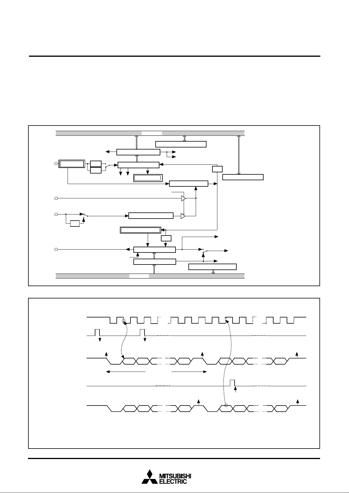
MITSUBISHI MICROCOMPUTERS
X
O E
P E
F E
D
R
A d d
R
R
)
R
)
Baud
F
)
Add
C
D
T
A d d
T
)
T
(TBE)
T
(TI)
A d d
S T d
SP d
UART
Add
B
Ch
A d d
A
B R G
t
T
bit
S
C l
C h
Serial I/O
P
S
S
r
P
RXD
P
TXD
TSC
R B F
T B E
T B E
RBF
R B F
S T
D0D
SP
D
0
D
S T
S P
TBE
S T
D0D
SP
D0D
ST
S P
T
l
bi
E
N
S
D
S
D
R
l
T
k
7560 Group
SINGLE-CHIP 8-BIT CMOS MICROCOMPUTER
(2) Asynchronous Serial I/O (UART) Mode
Clock asynchronous serial I/O mode (UART) can be selected by
clearing the serial I/O mode selection bit of the serial I/O1 control
register to “0”.
Eight serial data transfer formats can be selected, and the transfer
formats used by a transmitter and receiver must be identical.
The transmit and receive shift registers each have a buffer regis-
a t a b u
s
r e s s 0 0 1
a r a c t e r l e n g t h s e l e c t i o n b i
4
4
e t e c t o
/
r
7 b i t s
8 bits
e r i a l I / O 1 s y n c h r o n i z a t i o n c l o c k s e l e c t i o n b i
6
/
C L K 1
4
c o u n t s o u r c e s e l e c t i o n b i
IN
1/4
5
/
4
aracter length selection bit
1 6
8
e c e i v e b u f f e r r e g i s t e
t
e c e i v e s h i f t r e g i s t e
etector
requency division ratio 1/(n+1
rate generator
ress 001
ST/SP/PA generator
r a n s m i t s h i f t r e g i s t e
Transmi t buffer regis ter
r e s s 0 0 1
ata bus
r
r
1 control register
o c k c o n t r o l c i r c u i
t
16
1/16
r
ter, but the two buffers have the same address in memory. Since
the shift register cannot be written to or read from directly, transmit
data is written to the transmit buffer, and receive data is read from
the receive buffer.
The transmit buffer can also hold the next data to be transmitted,
and the receive buffer register can hold a character while the next
character is being received.
r e s s 0 0 1
e c e i v e b u f f e r f u l l f l a g ( R B F
e c e i v e i n t e r r u p t r e q u e s t ( R I
1 / 1 6
t
ransmit interrupt source selection
e r i a l I / O 1 s t a t u s r e g i s t e
1 6
8
1 6
control register
ress 001
r a n s m i t s h i f t r e g i s t e r s h i f t c o m p l e t i o n f l a g ( T S C
ransmit interrupt request
ransmit buffer empty flag
r e s s 0 0 1
16
1 6
9
Fig. 25 Block diagram of UART serial I/O1
r a n s m i t o r r e c e i v e c l o c
r a n s m i t b u f f e r w r i t e s i g n a
=
0
=0
TBE=1
e r i a l o u t p u t T x
e c e i v e b u f f e r r e a d s i g n a
e r i a l i n p u t R x
r r o r f l a g d e t e c t i o n o c c u r s a t t h e s a m e t i m e t h a t t h e R B F f l a g b e c o m e s “ 1 ” ( a t 1 s t s t o p b i t , d u r i n g r e c e p t i o n )
o t e s
1 :
2 : T h e t r a n s m i t i n t e r r u p t ( T I ) c a n b e g e n e r a t e d t o o c c u r w h e n e i t h e r t h e T B E o r T S C f l a g b e c o m e s “ 1 ” , d e p e n d i n g o n t h e s e t t i n g o f t h e t r a n s m i t i n t e r r u p t
s o u r c e s e l e c t i o n b i t ( T I C ) o f t h e s e r i a l I / O 1 c o n t r o l r e g i s t e r .
3 : T h e r e c e i v e i n t e r r u p t ( R I ) i s s e t w h e n t h e R B F f l a g b e c o m e s “ 1 ” .
Fig. 26 Operation of UART serial I/O1 function
=
0
1
1 start
7 or 8 data bits
1 or 0 parity bit
1 or 2 stop bit (s)
1
=1
1
t
=1
✽
G e n e r a t e d a t 2 n d b i t i n 2 - s t o p - b i t m o d e
=
0
1
.
T S C = 1
=
✽
1
29

[Transmit Buffer/Receive Buffer Register (TB/
RB)] 0018
The transmit buffer register and the receive buffer register are located at the same address. The transmit buffer register is writeonly and the receive buffer register is read-only. If a character bit
length is 7 bits, the MSB of data stored in the receive buffer register is “0”.
16
[Serial I/O1 Status Register (SIO1STS)]
16
0019
The read-only serial I/O1 status register consists of seven flags
(bits 0 to 6) which indicate the operating status of the serial I/O1
function and various errors.
Three of the flags (bits 4 to 6) are valid only in UART mode.
The receive buffer full flag (bit 1) is cleared to “0” when the receive
buffer is read.
If there is an error, it is detected at the same time that data is
transferred from the receive shift register to the receive buffer register, and the receive buffer full flag is set. A write to the serial I/O1
status register clears all the error flags OE, PE, FE, and SE (bit 3
to bit 6, respectively). Writing “0” to the serial I/O1 enable bit SIOE
(bit 7 of the Serial I/O1 Control Register) also clears all the status
flags, including the error flags.
All bits of the serial I/O1 status register are initialized to “0” at reset, but if the transmit enable bit (bit 4) of the serial I/O1 control
register has been set to “1”, the transmit shift register shift completion flag (bit 2) and the transmit buffer empty flag (bit 0) become
“1”.
MITSUBISHI MICROCOMPUTERS
7560 Group
SINGLE-CHIP 8-BIT CMOS MICROCOMPUTER
[Serial I/O1 Control Register (SIO1CON)]
16
001A
The serial I/O1 control register contains eight control bits for the
serial I/O1 function.
[UART Control Register (UARTCON)] 001B16
The UART control register consists of four control bits (bits 0 to 3)
which are valid when asynchronous serial I/O is selected and set
the data format of an data transfer. One bit in this register (bit 4) is
always valid and sets the output structure of the P45/TXD pin.
[Baud Rate Generator (BRG)] 001C16
The baud rate generator determines the baud rate for serial transfer.
The baud rate generator divides the frequency of the count source
by 1/(n + 1), where n is the value written to the baud rate generator.
■Notes on serial I/O
When setting the transmit enable bit to “1”, the serial I/O1 transmit
interrupt request bit is automatically set to “1”. When not requiring
the interrupt occurrence synchronous with the transmission
enalbed, take the following sequence.
➀Set the serial I/O1 transmit interrupt enable bit to “0” (disabled).
➁Set the transmit enable bit to “1”.
➂Set the serial I/O1 transmit interrupt request bit to “0” after 1 or
more instructions have been executed.
➃Set the serial I/O1 transmit interrupt enable bit to “1” (enabled).
30
MITSUBISHI MICROCOMPUTERS
B R G
)
Serial I/O
T
)
S
U A R T
C h
)
7560 Group
SINGLE-CHIP 8-BIT CMOS MICROCOMPUTER
b 7b
e r i a l I / O 1 s t a t u s r e g i s t e
0
( S I O 1 S T S : a d d r e s s 0 0 1 9
r a n s m i t b u f f e r e m p t y f l a g ( T B E
0 : B u f f e r f u l l
1 : B u f f e r e m p t y
R e c e i v e b u f f e r f u l l f l a g ( R B F )
0 : B u f f e r e m p t y
1 : B u f f e r f u l l
T r a n s m i t s h i f t r e g i s t e r s h i f t c o m p l e t i o n f l a g ( T S C )
0 : T r a n s m i t s h i f t i n p r o g r e s s
1 : T r a n s m i t s h i f t c o m p l e t e d
O v e r r u n e r r o r f l a g ( O E )
0 : N o e r r o r
1 : O v e r r u n e r r o r
P a r i t y e r r o r f l a g ( P E )
0 : N o e r r o r
1 : P a r i t y e r r o r
F r a m i n g e r r o r f l a g ( F E )
0 : N o e r r o r
1 : F r a m i n g e r r o r
S u m m i n g e r r o r f l a g ( S E )
0 : ( O E ) U ( P E ) U ( F E ) = 0
1 : ( O E ) U ( P E ) U ( F E ) = 1
N o t u s e d ( r e t u r n s “ 1 ” w h e n r e a d )
b 7b
c o n t r o l r e g i s t e r
0
( U A R T C O N : a d d r e s s 0 0 1 B
a r a c t e r l e n g t h s e l e c t i o n b i t ( C H A S
0 : 8 b i t s
1 : 7 b i t s
P a r i t y e n a b l e b i t ( P A R E )
0 : P a r i t y c h e c k i n g d i s a b l e d
1 : P a r i t y c h e c k i n g e n a b l e d
P a r i t y s e l e c t i o n b i t ( P A R S )
0 : E v e n p a r i t y
1 : O d d p a r i t y
S t o p b i t l e n g t h s e l e c t i o n b i t ( S T P S )
0 : 1 s t o p b i t
1 : 2 s t o p b i t s
5
P 4
0 : C M O S o u t p u t ( i n o u t p u t m o d e )
1 : N - c h a n n e l o p e n - d r a i n o u t p u t ( i n o u t p u t m o d e )
N o t u s e d ( r e t u r n “ 1 ” w h e n r e a d )
r
1 6
)
1 6
)
/ TXD P - c h a n n e l o u t p u t d i s a b l e b i t ( P O F F )
b 7b
0
(SIO1CON : address 001A
c o u n t s o u r c e s e l e c t i o n b i t ( C S S
0 : f ( X
1 : f ( X
S e r i a l I / O 1 s y n c h r o n i z a t i o n c l o c k s e l e c t i o n b i t ( S C S )
0 : B R G o u t p u t d i v i d e d b y 4 w h e n c l o c k s y n c h r o n o u s s e r i a l
I / O i s s e l e c t e d .
B R G o u t p u t d i v i d e d b y 1 6 w h e n U A R T i s s e l e c t e d .
1 : E x t e r n a l c l o c k i n p u t w h e n c l o c k s y n c h r o n o u s s e r i a l I / O i s
s e l e c t e d .
E x t e r n a l c l o c k i n p u t d i v i d e d b y 1 6 w h e n U A R T i s s e l e c t e d .
R D Y 1
S
0 : P 4
1 : P 4
T r a n s m i t i n t e r r u p t s o u r c e s e l e c t i o n b i t ( T I C )
0 : I n t e r r u p t w h e n t r a n s m i t b u f f e r h a s e m p t i e d
1 : I n t e r r u p t w h e n t r a n s m i t s h i f t o p e r a t i o n i s c o m p l e t e d
T r a n s m i t e n a b l e b i t ( T E )
0 : T r a n s m i t d i s a b l e d
1 : T r a n s m i t e n a b l e d
R e c e i v e e n a b l e b i t ( R E )
0 : R e c e i v e d i s a b l e d
1 : R e c e i v e e n a b l e d
S e r i a l I / O 1 m o d e s e l e c t i o n b i t ( S I O M )
0 : A s y n c h r o n o u s s e r i a l I / O ( U A R T )
1 : C l o c k s y n c h r o n o u s s e r i a l I / O
S e r i a l I / O 1 e n a b l e b i t ( S I O E )
0 : S e r i a l I / O 1 d i s a b l e d
( p i n s P 4
1 : S e r i a l I / O 1 e n a b l e d
( p i n s P 4
1 control register
I N
)
I N
) / 4
o u t p u t e n a b l e b i t ( S R D Y )
7
p i n o p e r a t e s a s o r d i n a r y I / O p i n
7
p i n o p e r a t e s a s S
4
– P 47 o p e r a t e a s o r d i n a r y I / O p i n s )
4
– P 47 o p e r a t e a s s e r i a l I / O p i n s )
16
)
R D Y 1
o u t p u t p i n
Fig. 27 Structure of serial I/O1 control registers
31

Serial I/O2
Serial I/O2 control register
(SIO2CON : address 001D
16
)
b7
Internal synchronous clock select bits
0 0 0: f(XIN)/8
0 0 1: f(X
IN
)/16
0 1 0: f(X
IN
)/32
0 1 1: f(X
IN
)/64
1 0 0:
1 0 1:
1 1 0: f(X
IN
)/128
1 1 1: f(X
IN
)/256
Serial I/O2 port selection bit
0: I/O port
1: S
OUT2,SCLK21/SCLK22
signal output
P6
1/SOUT2
P-channel output disable bit
0: CMOS output (in output mode)
1: N-channel open-drain output
(in output mode)
Transfer direction selection bit
0: LSB first
1: MSB first
Synchronous clock selection bit
0: External clock
1: Internal clock
Synchronous clock output pin selection bit
0: S
CLK21
1: S
CLK22
b0
b2 b1 b0
Do not set
The serial I/O2 function can be used only for clock synchronous
serial I/O.
For clock synchronous serial I/O2, the transmitter and the receiver
must use the same clock. When the internal clock is used, transfer
is started by a write signal to the serial I/O2 register.
When an internal clock is selected as the synchronous clock of the
serial I/O2, either P62 or P63 can be selected as an output pin of
the synchronous clock. In this case, the pin that is not selected as
an output pin of the synchronous clock functions as a port.
[Serial I/O2 Control Register (SIO2CON)] 001D16
The serial I/O2 control register contains 8 bits which control various serial I/O2 functions.
MITSUBISHI MICROCOMPUTERS
7560 Group
SINGLE-CHIP 8-BIT CMOS MICROCOMPUTER
X
IN
P63 latch
(Note)
P63/S
CLK22
P62/S
CLK21
P61/S
OUT2
P60/S
IN2
Note: It is selected by the synchronous clock selection bit, the synchronous
clock output pin selection bit, and the serial I/O port selection bit.
(Note)
Serial I/O2 port selection bit
Fig. 29 Block diagram of serial I/O2 function
P62 latch
“0”
“1”
1
latch
P6
“0”
“1”
Synchronous clock
selection bit
Synchronous circuit
CLK2
S
External clock
Fig. 28 Structure of serial I/O2 control register
1/8
1/16
1/32
1/64
Divider
1/128
1/256
“1”
“0”
Internal synchronous
clock select bits
Data bus
Serial I/O counter 2 (3)
Serial I/O shift register 2 (8)
Serial I/O2
interrupt request
32
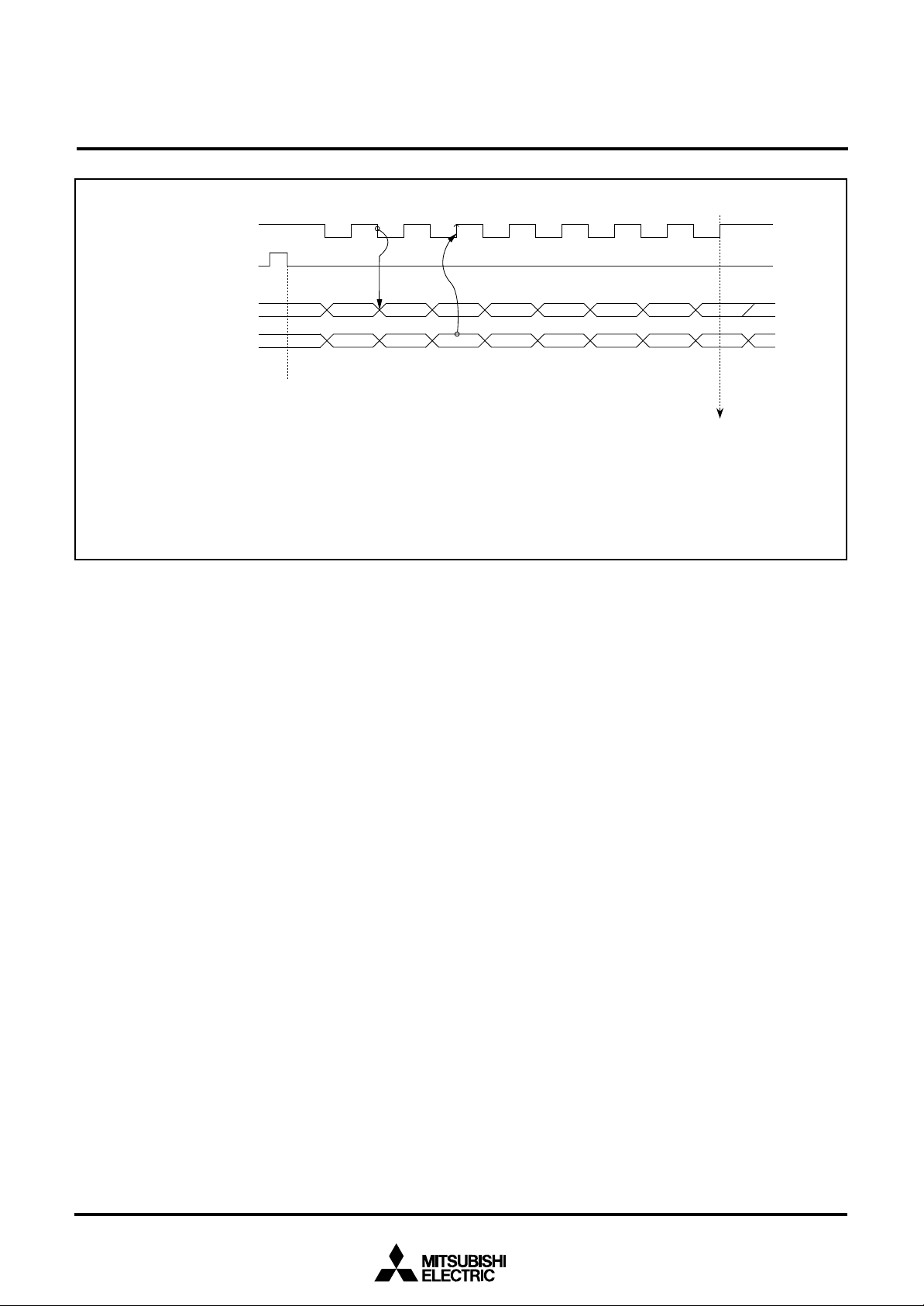
Transfer clock (Note 1)
Serial I/O2 register
write signal
Serial I/O2 output S
OUT2
MITSUBISHI MICROCOMPUTERS
7560 Group
SINGLE-CHIP 8-BIT CMOS MICROCOMPUTER
(Note 2)
D
D
0
D
2
1
D
3
D
4
D
5
D
6
D
7
Serial I/O2 input S
Notes
1: When the internal clock is selected as the transfer clock, the divide ratio can be selected by setting bits 0 to 2 of the serial
2: When the internal clock is selected as the transfer clock, the S
When the external clock is selected as the transfer clock, a content of the serial I/O shift register is continued to shift
IN2
I/O2 control register.
during inputting a transfer clock. The S
Fig. 30 Timing of serial I/O2 function
Serial I/O2 interrupt request bit set
OUT2
pin goes to high impedance after transfer completion.
OUT2
pin does not go to high impedance after transfer completion.
33

MITSUBISHI MICROCOMPUTERS
D
C
”
”
P W M
PWM
P W M
P W M
T
PWM ci
X
PWM
P
P W M
PWM
P
P
P
7560 Group
SINGLE-CHIP 8-BIT CMOS MICROCOMPUTER
PULSE WIDTH MODULATION (PWM)
The 7560 group has a PWM function with an 8-bit resolution,
based on a signal that is the clock input XIN or that clock input divided by 2.
Data Setting
The PWM output pin also functions as ports P50 and P51. Set the
PWM period by the PWM prescaler, and set the period during
which the output pulse is an “H” by the PWM register.
If PWM count source is f(XIN) and the value in the PWM prescaler
is n and the value in the PWM register is m (where n = 0 to 255
and m = 0 to 255) :
PWM period = 255 ✕ (n+1)/f(XIN)
= 31.875 ✕ (n+1) µs (when f(XIN) = 8 MHz)
Output pulse “H” period = PWM period ✕ m/255
= 0.125 ✕ (n+1) ✕ m µs
(when f(XIN) = 8 MHz)
PWM Operation
When at least either bit 1 (PWM0 function enable bit) or bit 2
(PWM1 function enable bit) of the PWM control register is set to
“1”, operation starts by initializing the PWM output circuit, and
pulses are output starting at an “H”. When one PWM output is enabled and that the other PWM output is enabled, PWM output
which is enabled to output later starts pulse output from halfway.
When the PWM register or PWM prescaler is updated during
PWM output, the pulses will change in the cycle after the one in
which the change was made.
31.875 ✕ m ✕ (n+1)
PWM output
m: Contents of PWM register
n : Contents of PWM prescaler
T : PWM cycle (when f(X
Fig. 31 Timing of PWM cycle
255
T = [31.875 ✕ (n+1)] µs
IN
) = 8 MHz)
µs
ata bus
p r e s c a l e r p r e - l a t c h
p r e s c a l e r l a t c h
o u n t s o u r c e
s e l e c t i o n b i t
1 / 2
“ 0
“ 1
IN
p r e s c a l e
Fig. 32 Block diagram of PWM function
ransfer con trol circuit
r
register pre-latch
r e g i s t e r l a t c h
rcuit
o r t P
l a c t h
ort P5
lacth
enable bit
1
5
0
0
function
enable bit
1
function
o r t P
ort P5
1
5
0
34

MITSUBISHI MICROCOMPUTERS
7560 Group
SINGLE-CHIP 8-BIT CMOS MICROCOMPUTER
b7
b0
PWM control register
(PWMCON : address 002B16)
Count source selection bit
0: f(XIN)
1: f(XIN)/2
PWM0 function enable bit
0: PWM0 disabled
1: PWM
1
function enable bit
PWM
0: PWM1 disabled
1: PWM1 enabled
Not used (return “0” when read)
Fig. 33 Structure of PWM control register
A
PWM
(internal)
stop
0
enabled
T
C
B
B
T
C
T2
=
T2
T
stop
PWM
0
output
PWM1 output
PWM register
write signal
PWM prescaler
write signal
PWM0 function
enable bit
1
function
PWM
enable bit
Port
Port
(Changes from “A” to “B” during “H” period)
(Changes from “T” to “T2” during PWM period)
When the contents of the PWM register or PWM prescaler have changed, the PWM
output will change from the next period after the change.
Port
Port
Fig. 34 PWM output timing when PWM register or PWM prescaler is changed
35

MITSUBISHI MICROCOMPUTERS
A
A D
A
V
A D
b
b
I
N
)
C
A-D
it
ADT/A-D i
A V
S
V
P
S
A N
D
s
A
b
b
A-D
Resi
r
P
A N
P
A N
P
A N
P
A N
P
S
AN
P
S
AN
P
S
A N
P
A D T
A
7560 Group
SINGLE-CHIP 8-BIT CMOS MICROCOMPUTER
A-D CONVERTER
The functional blocks of the A-D converter are described below.
[A-D Conversion Register (AD)] 003516
The A-D conversion register is a read-only register that contains
the result of an A-D conversion. When reading this register during
an A-D conversion, the previous conversion result is read.
[A-D Control Register (ADCON)] 003416
The A-D control register controls the A-D conversion process. Bits
0 to 2 of this register select specific analog input pins. Bit 3 signals
the completion of an A-D conversion. The value of this bit remains
at “0” during an A-D conversion, then changes to “1” when the AD conversion is completed. Writing “0” to this bit starts the A-D
conversion. Bit 4 controls the transistor which breaks the through
current of the resistor ladder. When bit 5, which is the AD external
trigger valid bit, is set to “1”, this bit enables A-D conversion even
by a falling edge of an ADT input. Set ports which share with ADT
pins to input when using an A-D external trigger.
Comparison Voltage Generator
The comparison voltage generator divides the voltage between
AVSS and VREF by 256, and outputs the divided voltages.
Channel Selector
The channel selector selects one of the input ports P67/AN7–P60/
AN0.
Comparator and Control Circuit
The comparator and control circuit compare an analog input voltage with the comparison voltage and store the result in the A-D
conversion register. When an A-D conversion is completed, the
control circuit sets the AD conversion completion bit and the AD
interrupt request bit to “1”.
Note that the comparator is constructed linked to a capacitor, so
set f(XIN) to at least 500kHz during A-D conversion.
Use the clock divided from the main clock X
φ.
7
- D c o n t r o l r e g i s t e
0
( A D C O N : a d d r e s s 0 0 3 4
n a l o g i n p u t p i n s e l e c t i o n b i t
0 0 0 : P 60/ A N
0 0 1 : P 61/ A N
0 1 0 : P 62/ A N
0 1 1 : P 63/ A N
1 0 0 : P 64/ A N
1 0 1 : P 65/ A N
1 1 0 : P 66/ A N
1 1 1 : P 67/ A N
c o n v e r s i o n c o m p l e t i o n b i
0 : C o n v e r s i o n i n p r o g r e s s
1 : C o n v e r s i o n c o m p l e t e d
REF
input switch bit
0 : OFF
1 : ON
e x t e r n a l t r i g g e r v a l i d b i
0 : A - D e x t e r n a l t r i g g e r i n v a l i d
1 : A - D e x t e r n a l t r i g g e r v a l i d
n t e r r u p t s o u r c e s e l e c t i o n b i
0 : I n t e r r u p t r e q u e s t a t A - D
c o n v e r s i o n c o m p l e t e d
1 : I n t e r r u p t r e q u e s t a t A D T
i n p u t f a l l i n g
o t u s e d ( r e t u r n s “ 0 ” w h e n r e a d
IN as the internal clock
r
1 6
)
s
0
1
2
3
4
5
6
7
t
t
t
a t a b u
- D c o n t r o l r e g i s t e
/ D
7
/
I N 2
O U T2
2
/
0
/
1
/
2
/
3
4
/
4
6
5
/
5
6
6
/
6
6
7
/
7
6
5
0
/
6
1
/
6
62/
CLK21
63/
CLK22
Fig. 36 A-D converter block diagram
36
Fig. 35 Structure of A-D control register
7
r
3
control circu
r
C
h a n n e l s e l e c t o
o m p a r a t o
r
conversion
register
stor ladde
S
0
nterrupt request
8
REF

D-A Converter
The 7560 group has an on-chip D-A converter with 8-bit resolution
and 2 channels (DAi (i=1, 2)). After the DA
selection bit is set to “0”, the D-A converter is performed by setting
the value in the D-A conversion register. The result of D-A converter is output from DAi pin. When using the D-A converter, the
corresponding port direction register bit (P56/DA1, P5 7/DA2)
should be set to “0” (input status) and the pull-up resistor should
be in the OFF state.
The output analog voltage V is determined by the value n (base
10) in the D-A conversion register as follows:
V=VREF ✕ n/256 (n=0 to 255)
Where VREF is the reference voltage.
1 selection bit or DA2
MITSUBISHI MICROCOMPUTERS
7560 Group
SINGLE-CHIP 8-BIT CMOS MICROCOMPUTER
b7
b0
D-A control register
(DACON : address 0036
DA1 output enable bit
0 : Disabled
1 : Enabled
2
output enable bit
DA
0 : Disabled
1 : Enabled
Not used (return “0” when read)
(Do not write “1” to these bits.)
16
)
At reset, the D-A conversion registers are cleared to “0016”, the
DAi output enable bits are cleared to “0”, and DAi pin goes to
high impedance state. The DA output is not buffered, so connect
an external buffer when driving a low-impedance load.
■ Note on applied voltage to VREF pin
When the P56/DA1 pin and P57/DA2 pin are used as I/O ports, be
sure to apply Vcc level to VREF pin.
When these pins are used as D-A conversion output pins, the Vcc
level is recommended for the applied voltage to VREF pin.
When the voltage below Vcc level is applied, the D-A conversion
accuracy may be worse.
Fig. 37 Structure of D-A control register
Data bus
D - A 1 c o n v e r s i o n r e g i s t e r
( D A 1 : a d d r e s s 0 0 3 2
D - A 2 c o n v e r s i o n r e g i s t e r
( D A 2 : a d d r e s s 0 0 3 3
D-A i conversion register (8)
D A i o u t p u t e n a b l e b i t
R-2R resistor ladder
Fig. 38 Block diagram of D-A converter
1 6
)
1 6
)
P5
6
P57/DA
/DA
1
2
37
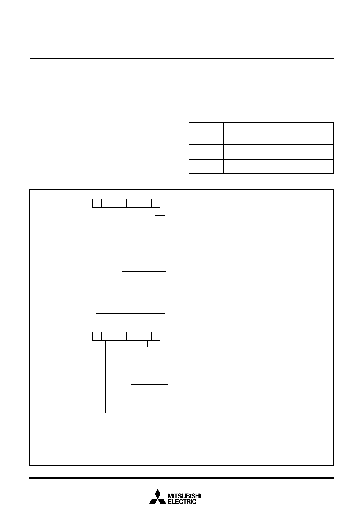
MITSUBISHI MICROCOMPUTERS
S
S
b7b
L C D
D
N
b
b
7560 Group
SINGLE-CHIP 8-BIT CMOS MICROCOMPUTER
LCD DRIVE CONTROL CIRCUIT
The 7560 group has the built-in Liquid Crystal Display (LCD) drive
control circuit consisting of the following.
LCD display RAM
•
Segment output enable register
•
LCD mode register
•
Voltage multiplier
•
Selector
•
Timing controller
•
Common driver
•
Segment driver
•
Bias control circuit
•
A maximum of 40 segment output pins and 4 common output pins
can be used.
Up to 160 pixels can be controlled for LCD display. When the LCD
7
o t e : L C D C K i s a c l o c k f o r a L C D t i m i n g c o n t r o l l e r
0
egment output enable register
(SEG : address 0038
e g m e n t o u t p u t e n a b l e b i t
0 : O u t p u t p o r t s P 3
1 : S e g m e n t o u t p u t S E G
S e g m e n t o u t p u t e n a b l e b i t 1
0 : O u t p u t p o r t s P 3
1 : S e g m e n t o u t p u t S E G
S e g m e n t o u t p u t e n a b l e b i t 2
0 : I / O p o r t s P 0
1 : S e g m e n t o u t p u t S E G
S e g m e n t o u t p u t e n a b l e b i t 3
0 : I / O p o r t s P 0
1 : S e g m e n t o u t p u t S E G
S e g m e n t o u t p u t e n a b l e b i t 4
0 : I / O p o r t P 1
1 : S e g m e n t o u t p u t S E G
S e g m e n t o u t p u t e n a b l e b i t 5
0 : I / O p o r t s P 1
1 : S e g m e n t o u t p u t S E G
L C D o u t p u t e n a b l e b i t
0 : D i s a b l e d
1 : E n a b l e d
N o t u s e d ( r e t u r n “ 0 ” w h e n r e a d )
( D o n o t w r i t e “ 1 ” t o t h i s b i t )
0
m o d e r e g i s t e
( L M : a d d r e s s 0 0 3 9
enable bit is set to “1” after data is set in the LCD mode register,
the segment output enable register and the LCD display RAM, the
LCD drive control circuit starts reading the display data automatically, performs the bias control and the duty ratio control, and displays the data on the LCD panel.
Table 9. Maximum number of display pixels at each duty ratio
Duty ratio Maximum number of display pixel
2
3
4
16
)
0
6
0
– P 0
6
, P 0
7
0
1
– P 1
r
1 6
C I N
) / 3 2
I N
) / 8 1 9 2 ( f ( X
)
.
u t y r a t i o s e l e c t i o n b i t
0 0 : N o t u s e d
0 1 : 2 d u t y ( u s e C O M
1 0 : 3 d u t y ( u s e C O M
1 1 : 4 d u t y ( u s e C O M
B i a s c o n t r o l b i t
0 : 1 / 3 b i a s
1 : 1 / 2 b i a s
L C D e n a b l e b i t
0 : L C D O F F
1 : L C D O N
V o l t a g e m u l t i p l i e r c o n t r o l b i t
0 : V o l t a g e m u l t i p l i e r d i s a b l e
1 : V o l t a g e m u l t i p l i e r e n a b l e
L C D c i r c u i t d i v i d e r d i v i s i o n r a t i o s e l e c t i o n b i t s
0 0 : C l o c k i n p u t
0 1 : 2 d i v i s i o n o f C l o c k i n p u t
1 0 : 4 d i v i s i o n o f C l o c k i n p u t
1 1 : 8 d i v i s i o n o f C l o c k i n p u t
L C D C K c o u n t s o u r c e s e l e c t i o n b i t ( N o t e )
0 : f ( X
1 : f ( X
80 dots
or 8 segment LCD 10 digits
120 dots
or 8 segment LCD 15 digits
160 dots
or 8 segment LCD 20 digits
0
– P 3
5
1 8
– S E G
2 3
, P 3
7
2 4
, S E G
2 5
5
2 6
– S E G
3 1
3 2
, S E G
3 3
3 4
5
3 5
– S E G
3 9
s
0
, C O M1)
0
– C O M2)
0
– C O M3)
C I N
) / 8 1 9 2 i n l o w - s p e e d m o d e )
Fig. 39 Structure of segment output enable register and LCD mode register
38

Fig. 40 Block diagram of LCD controller/driver
D a t a b u s
A d d r e s s 0 0 4 0
1 6
A d d r e s s 0 0 4 1
1 6
A d d r e s s 0 0 5 3
1 6
L C D d i s p l a y R A M
V o l t a g e m u l t i p l i e r
c o n t r o l b i t
B i a s c o n t r o l b i t
L C D e n a b l e b i t
D u t y r a t i o s e l e c t i o n b i t s
L C D c i r c u i t
d i v i d e r d i v i s i o n
r a t i o s e l e c t i o n b i t s
2
2
L C D C K c o u n t s o u r c e
s e l e c t i o n b i t
L C D
d i v i d e r
“ 0 ”
“ 1 ”
f ( X
C I N
) / 3 2
f ( X
I N
) / 8 1 9 2
C I N
) / 8 1 9 2 i n l o w -
( f ( X
s p e e d m o d e )
S e l e c t o rS e l e c t o rS e l e c t o r
L e v e l
L e v e l
s h i f t
d r i v e r
1
L e v e l
s h i f t
S e g m e n t
d r i v e r
S E G
s h i f t
S e g m e n t
d r i v e r
S E G
0
S e g m e n t
S E G
2
S e l e c t o r
L e v e l
s h i f t
S e g m e n t
d r i v e r
S E G
S e l e c t o r
S e l e c t o r
L e v e l
s h i f t
L e v e l
s h i f t
B i a s c o n t r o l
T i m i n g c o n t r o l l e r
L e v e l
L e v e l
L e v e l
S h i f t
S h i f t
V
C C
S h i f t
L e v e l
S h i f t
L C D C K
SINGLE-CHIP 8-BIT CMOS MICROCOMPUTER
S e g m e n t
d r i v e r
S e g m e n t
d r i v e r
L C D o u t p u t
e n a b l e b i t
C o m m o n
d r i v e r
C o m m o n
d r i v e r
C o m m o n
d r i v e r
C o m m o n
d r i v e r
MITSUBISHI MICROCOMPUTERS
7560 Group
V
3
P 30/ S E G
P 14/ S E G
3 8
P 15/ S E G
1 8
3 9
S SVL 1VL 2VL 3
C1C
2
C O M
0
C O M1C O M
C O M
3
2
39
MITSUBISHI MICROCOMPUTERS
V
V
C2C
V
b i
V
V
C
C
V
b i
O
O
R
R
R
R
C
l
V
V
C2C
V
b i
O
O
R
R
R4=R
C
l
PX
7560 Group
SINGLE-CHIP 8-BIT CMOS MICROCOMPUTER
Voltage Multiplier (3 Times)
The voltage multiplier performs threefold boosting. This circuit inputs a reference voltage for boosting from LCD power input pin
L1. (However, when using a 1/2 bias, connect VL1 and VL2 and
V
apply voltage by external resistor division.)
Set each bit of the segment output enable register and the LCD
mode register in the following order for operating the voltage multiplier.
1. Set the segment output enable bits (bits 0 to 5) of the segment output enable register to “0” or “1.”
2. Set the duty ratio selection bits (bits 0 and 1), the bias control bit (bit 2), the LCD circuit divider division ratio selection
bits (bits 5 and 6), and the LCDCK count source selection
bit (bit 7) of the LCD mode register to “0” or “1.”
3. Set the LCD output enable bit (bit 6) of the segment output
enable register to “1.”
4. Set the voltage multiplier control bit (bit 4) of the LCD mode
register to “1.”
When voltage is input to the V
multiplier, voltage that is twice as large as VL1 occurs at the VL2
pin, and voltage that is three times as large as VL1 occurs at the
VL3 pin.
When using the voltage multiplier, apply 1.3 V ≤ Voltage ≤ 2.1 V to
the VL1 pin.
When not using the voltage multiplier,apply proper voltage to the
LCD power input pins (VL1–VL3). Then set the LCD output enable
bit to “1.”
When the LCD output enable bit is set to “0,” the VCC voltage is
applied to the VL3 pin inside of this microcomputer.
The voltage multiplier control bit (bit 4 of the LCD mode register)
controls the voltage multiplier.
L1 pin during operating the voltage
Bias Control and Applied Voltage to LCD
Power Input Pins
To the LCD power input pins (VL1–VL3), apply the voltage shown
in Table 10 according to the bias value.
Select a bias value by the bias control bit (bit 2 of the LCD mode
register).
Table 10. Bias control and applied voltage to VL1–VL3
Bias value
VL3=VLCD
1/3 bias
VL2=2/3 VLCD
VL1=1/3 VLCD
VL3=VLCD
1/2 bias
VL2=VL1=1/2 VLCD
Note : VLCD is the maximum value of supplied voltage for the
LCD panel.
Voltage value
L 3
L 2
1
L 1
a
1 / 3
s
w h e n u s i n g t h e v o l t a g e m u l t i p l i e r
o n t r a s t c o n t r o
L 3
L 2
p e
2
p e
1
L 1
a
1 / 3
s
w h e n n o t u s i n g t h e v o l t a g e m u l t i p l i e r
1
n
2
n
3
1 = R 2 = R
3
a
1 / 2
L 3
L 2
p e
p e
1
L 1
x
s
o n t r a s t c o n t r o
4
n
n
5
5
Fig. 41 Example of circuit at each bias
40

MITSUBISHI MICROCOMPUTERS
B i t
Add
S E G
C O M3C O M0C O M2C O M1C O M0C O M3C O M2C O M
S E G
7560 Group
SINGLE-CHIP 8-BIT CMOS MICROCOMPUTER
Common Pin and Duty Ratio Control
The common pins (COM0–COM3) to be used are determined by
duty ratio.
Select duty ratio by the duty ratio selection bits (bits 0 and 1 of the
LCD mode register).
When releasing from reset, the VCC (VL3) voltage is output from
the common pins.
Table 11. Duty ratio control and common pins used
Duty
Duty ratio selection bits
ratio
Bit 1
2
3
4
0
1
1
Bit 0
1
0
1
Common pins used
COM0, COM1 (Note 1)
COM0–COM2 (Note 2)
COM0–COM3
Notes 1: COM2 and COM3 are open.
2: COM3 is open.
Segment Signal Output Pin
Segment signal output pins are classified into the segment-only
pins (SEG0–SEG 17), the segment/output port pins (SEG18–
SEG25), and the segment/I/O port pins (SEG26–SEG39).
Segment signals are output according to the bit data of the LCD
RAM corresponding to the duty ratio. After reset release, a VCC
(=VL3) voltage is output to the segment-only pins and the segment/output port pins are the high impedance condition and
pulled up to VCC (=VL3) voltage.
Also, the segment/I/O port pins(SEG26–SEG39) are set to input
ports, and VCC (=VL3) is applied to them by pull-up resistor.
LCD Display RAM
Address 004016 to 005316 is the designated RAM for the LCD display. When “1” are written to these addresses, the corresponding
segments of the LCD display panel are turned on.
LCD Drive Timing
The LCDCK timing frequency (LCD drive timing) is generated internally and the frame frequency can be determined with the following equation;
(frequency of count source for LCDCK)
f(LCDCK)=
(divider division ratio for LCD)
f(LCDCK)
Frame frequency=
duty ratio
Fig. 42 LCD display RAM map
ress
0 0 4 01
0 0 4 11
0 0 4 21
0 0 4 31
0 0 4 41
0 0 4 51
0 0 4 61
0 0 4 71
0 0 4 81
0 0 4 91
0 0 4 A1
0 0 4 B1
0 0 4 C1
0 0 4 D1
0 0 4 E1
0 0 4 F1
0 0 5 01
0 0 5 11
0 0 5 21
0 0 5 31
76543210
6
6
6
6
6
6
6
6
6
6
6
6
6
6
6
6
6
6
6
6
S E G3
S E G5
S E G7
S E G9
S E G1
S E G1
S E G1
S E G1
S E G1
S E G2
S E G2
S E G2
S E G2
S E G2
S E G3
S E G3
S E G3
S E G3
S E G3
1
1
3
5
7
9
1
3
5
7
9
1
3
5
7
9
S E G2
S E G4
S E G6
S E G8
S E G1
S E G1
S E G1
S E G1
S E G1
S E G2
S E G2
S E G2
S E G2
S E G2
S E G3
S E G3
S E G3
S E G3
S E G3
1
0
0
2
4
6
8
0
2
4
6
8
0
2
4
6
8
41
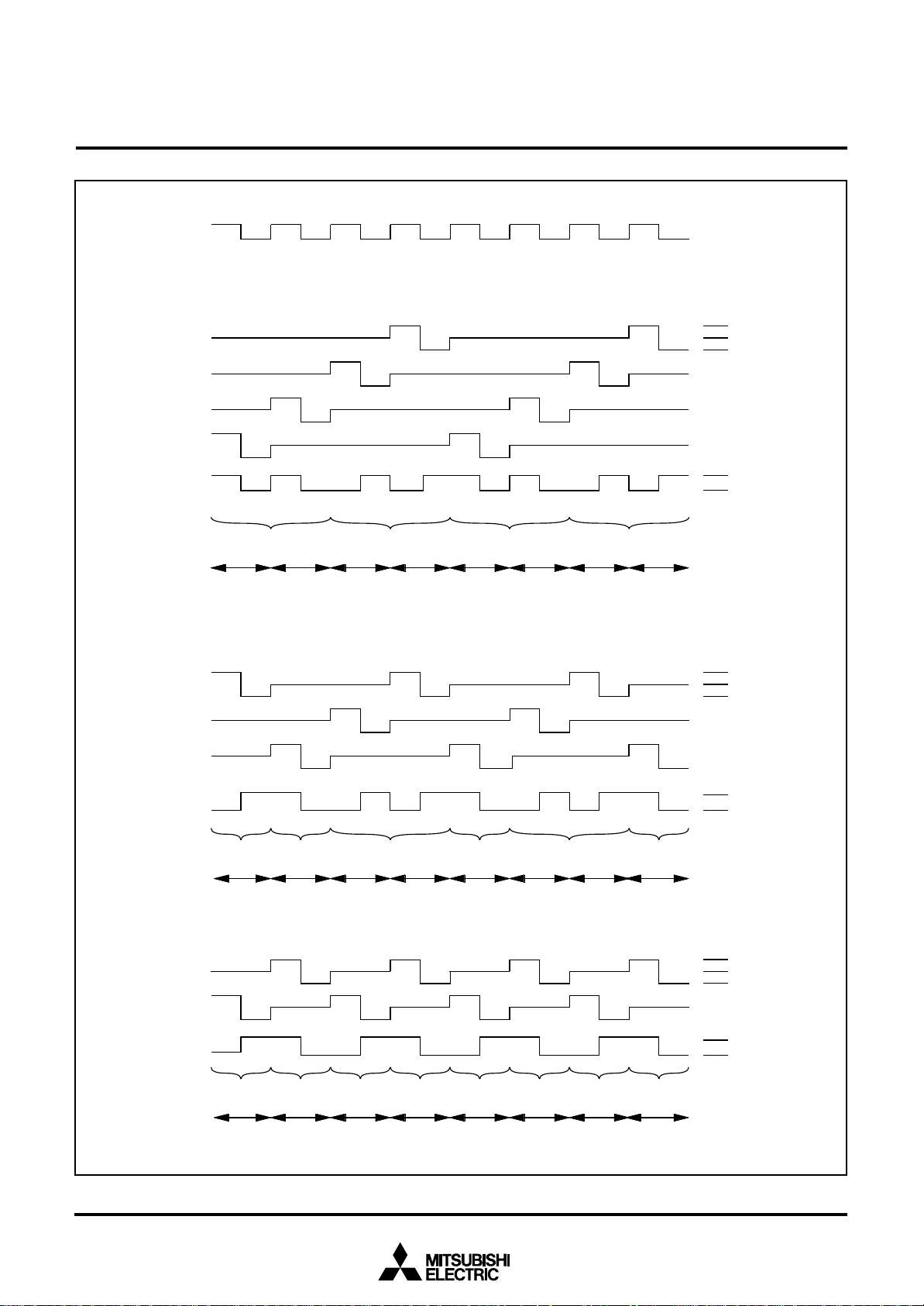
I n t e r n a l l o g i c
L C D C K t i m i n g
MITSUBISHI MICROCOMPUTERS
7560 Group
SINGLE-CHIP 8-BIT CMOS MICROCOMPUTER
1 / 4 d u t y
C O M
C O M
C O M
C O M
S E G
1 / 3 d u t y
COM
C O M
Voltage level
V
L 3
V
L 2
= V
0
1
2
3
0
L 1
V
S S
V
L 3
V
SS
OFF ON OFF ON
COM
3
COM2COM1COM
0
1
COM
0
3
COM2COM
1
COM
0
V
L 3
V
L 2
= V
L 1
V
SS
C O M
2
S E G
0
O F FO N O NOFFO NO
COM0C O M2C O M
1 / 2 d u t y
C O M
0
C O M
1
SEG
0
OFFON OFFON OFFON OFFON
COM1C O M0C O M
Fig. 43 LCD drive waveform (1/2 bias)
V
L3
V
SS
F
F
COM
COM
0
C O M2C O M1COM0COM
0
C O M1C O M0COM1COM
2
V
L 3
V
L 2
= V
L 1
V
S S
V
L 3
V
S S
0
1
1
42

I n t e r n a l l o g i c
L C D C K t i m i n g
MITSUBISHI MICROCOMPUTERS
7560 Group
SINGLE-CHIP 8-BIT CMOS MICROCOMPUTER
1 / 4 d u t y
C O M0
C O M1
C O M2
C O M3
S E G0
1/3 duty
COM
C O M1
V o l t a g e l e v e l
VL
3
VL
2
VL
1
VS
S
VL
3
VS
S
O F FO
COM3
0
COM2 COM1 COM0
N O F FON
COM3
COM2 COM1 COM0
VL
VL2
VL
VS
3
1
S
COM2
SEG0
1 / 2 d u t y
C O M0
COM1
S E G0
OFFO N O NO
COM0
C O M2 C O M1 C O M0
OFFON OFFON OFFON OFFON
C O M1 C O M0
C O M1 C O M0
F
F ON O F F
COM2 COM1 COM0 COM2
COM1 C O M0 C O M1 C O M0
VL
VS
VL
VL
VL
VSS
VL
VS
3
S
3
2
1
3
S
Fig. 44 LCD drive waveform (1/3 bias)
43

MITSUBISHI MICROCOMPUTERS
7560 Group
SINGLE-CHIP 8-BIT CMOS MICROCOMPUTER
Watchdog Timer
The watchdog timer gives a mean of returning to the reset status
when a program cannot run on a normal loop (for example, because of a software runaway).
The watchdog timer consists of an 8-bit watchdog timer L and a 6bit watchdog timer H. At reset or writing to the watchdog timer
control register (address 003716), the watchdog timer is set to
“3FFF16.” When any data is not written to the watchdog timer control register (address 003716) after reset, the watchdog timer is in
stop state. The watchdog timer starts to count down from “3FFF16”
by writing an optional value into the watchdog timer control register (address 003716) and an internal reset occurs at an underflow.
Accordingly, programming is usually performed so that writing to
the watchdog timer control register (address 003716) may be
started before an underflow. The watchdog timer does not function
when an optional value has not been written to the watchdog timer
control register (address 003716). When address 003716 is read,
the following values are read:
“FF16” is set when
“1”
“0”
STP instruction
watchdog timer is
written to.
1/16
Undefined instruction
Watchdog timer
L (8)
Reset
X
CIN
Internal
system clock
selection bit
(Note)
X
IN
STP instruction disable bit
RESET
Note: This is the bit 7 of CPU mode register and is used to switch the middle-/high-speed mode and low-speed mode.
Fig. 45 Block diagram of watchdog timer
●value of high-order 6-bit counter
●value of STP instruction disable bit
●value of count source selection bit.
When bit 6 of the watchdog timer control register (address 003716)
is set to “0,” the STP instruction is valid. The STP instruction is
disabled by rewriting this bit to “1.” At this time, if the STP instruction is executed, it is processed as an undefined instruction, so
that a reset occurs inside.
This bit cannot be rewritten to “0” by programming. This bit is “0”
immediately after reset.
The count source of the watchdog timer becomes the system
clock φ divided by 8. The detection time in this case is set to 8.19 s
at f(XCIN) = 32 kHz and 32.768 ms at f(XIN) = 8 MHz.
However, count source of high-order 6-bit timer can be connected
to a signal divided system clock by 8 directly by writing the bit 7 of
the watchdog timer control register (address 003716) to “1.” The
detection time in this case is set to 32 ms at f(XCIN) = 32 kHz and
128 µs at f(XIN) = 8 MHz. There is no difference in the detection
time between the middle-speed mode and the high-speed mode.
Data bus
Watchdog timer H count
source selection bit
“0”
“1”
Watchdog timer
H (6)
Reset circuit
Reset release time wait
“3F16” is set when
watchdog timer is
written to.
Internal reset
b 7 b 0
Fig. 46 Structure of watchdog timer control register
f ( X
I N
)
I n t e r n a l
r e s e t s i g n a l
W a t c h d o g t i m e r d e t e c t i o n
Fig. 47 Timing of reset output
44
1 6
W a t c h d o g t i m e r r e g i s t e r ( a d d r e s s 0 0 3 7
W D T C O N
W a t c h d o g t i m e r H ( f o r r e a d - o u t o f h i g h - o r d e r 6 b i t )
“ 3 F F F
1 6
” i s s e t t o t h e w a t c h d o g t i m e r b y w r i t i n g v a l u e s t o t h i s a d d r e s s .
S T P i n s t r u c t i o n d i s a b l e b i t
0 : S T P i n s t r u c t i o n e n a b l e d
1 : S T P i n s t r u c t i o n d i s a b l e d
Watchdog timer H count source selecion bit
0 : Watchdog timer L underfl ow
1 : f(X
IN
≅ 1
m s
)/16 or f(X
( f ( X
I N
) = 8 M HZ)
CIN
)/16
)

TOUT/φ CLOCK OUTPUT FUNCTION
The internal system clock φ or timer 2 divided by 2 (TOUT output)
can be output from port P43 by setting the TOUT/φ output control
bit (bit 1) of the timer 123 mode register and the TOUT/φ output
control register. Set bit 3 of the port P4 direction register to “1”
when outputting the clock.
MITSUBISHI MICROCOMPUTERS
7560 Group
SINGLE-CHIP 8-BIT CMOS MICROCOMPUTER
b7 b0
b7 b0
T
OUT
/φ output control register
(CKOUT : address 002A
T
OUT
/φ output control bit
0 : φ clock output
1 : T
OUT
Not used (return “0” when read)
Timer 123 mode register
(T123M : address 0029
output
T
OUT
output active edge switch bit
0 : Start at “H” output
1 : Start at “L” output
T
OUT
/φ output control bit
0 : T
OUT
/φ output disabled
1 : T
OUT
Timer 2 write control bit
Timer 2 count source selection bit
Timer 3 count source selection bit
Timer 1 count source selection bit
/φ output enabled
0 : Write data in latch and timer
1 : Write data in latch only
0 : Timer 1 output
1 : f(X
IN
)/16
(or f(X
CIN
0 : Timer 1 output
1 : f(X
IN
)/16
(or f(X
CIN
0 : f(X
IN
)/16
(or f(X
CIN
1 : f(X
CIN
16
)
16
)
)/16 in low-speed mode✽)
)/16 in low-speed mode✽)
)/16 in low-speed mode✽)
)
Not used (return “0” when read)
Fig. 48 Structure of TOUT/
✽ : Internal clock φ is f(X
φφ
φ output-related register
φφ
CIN
)/2 in the low-speed mode.
45
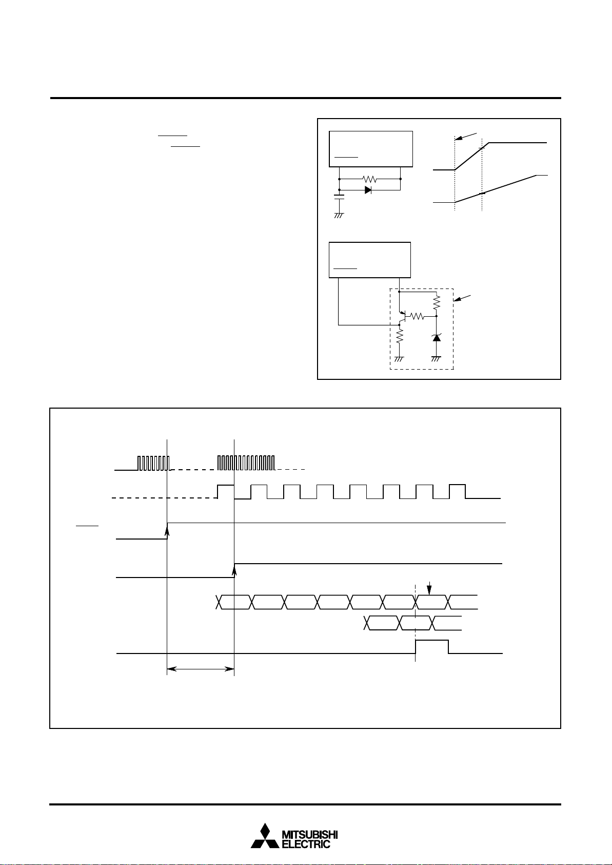
MITSUBISHI MICROCOMPUTERS
P o w e r s o u r c e v o l t a g e
d e t e c t i o n c i r c u i t
N o t e : R e s e t r e l e a s e v o l t a g e V
C C
= V
C C
( m i n . )
A D
FFFC
F F F D
A DH,???
?
X
b
N
X
d
f(XIN)
f(φ)
R
R E S E T
I
A d d
D
S Y N C
φ
X
A D
AD
7560 Group
SINGLE-CHIP 8-BIT CMOS MICROCOMPUTER
RESET CIRCUIT
To reset the microcomputer, RESET pin should be held at an “L”
level for 2 µs or more. Then the RESET pin is returned to an “H”
level (the power source voltage should be between VCC(min.) and
5.5 V, and the quartz-crystal oscillator should be stable), reset is
released. After the reset is completed, the program starts from the
address contained in address FFFD16 (high-order byte) and address FFFC16 (low-order byte). Make sure that the reset input
voltage is less than 0.2 VCC for VCC of VCC (min.).
P o w e r
s o u r c e
R E S E T
v o l t a g e
V
C C
0V
R e s e t i n p u t
v o l t a g e
0V
V
R E S E T
CC
Fig. 49 Example of reset circuit
P o w e r o n
(N o t e)
0 . 2 V
C C
IN
n t e r n a l r e s e
r e s
a t
t
s
a
Fig. 50 Reset Sequence
: a
o u t 8 2 0 0
I N
c l o c k c y c l e s
e s e t a d d r e s s f r o m
v e c t o r t a b l e
L
otes 1 :
IN an
2 : A question mark (?) indicates an undefi ned status that depends on the previous status.
φ are in the relationship :
H
= 8•
L
46
MITSUBISHI MICROCOMPUTERS
N
Regi
Add
B
D
F
A
B
D
A
B
A
B
C
D
E
F
(PS)
(PCH)
( P CL)
(10)
(11)
(12)
(13)
(14)
(15)
(16)
(17)
(18)
(19)
(20)
(21)
(22)
(23)
(24)
(25)
(26)
(27)
(28)
(29)
(30)
(31)
(32)
(33)
(34)
(1)
(2)
(3)
(4)
(5)
(6)
(7)
(8)
(9)
(35)
(36)
(37)
(38)
(39)
(40)
(41)
(42)
(43)
FF
FF
FF
F
FF
FF
(44)
FF
F
FF
7560 Group
SINGLE-CHIP 8-BIT CMOS MICROCOMPUTER
P o r t P 0 d i r e c t i o n r e g i s t e r
P o r t P 1 d i r e c t i o n r e g i s t e r
P o r t P 2 d i r e c t i o n r e g i s t e r
P o r t P 3 o u t p u t c o n t r o l r e g i s t e r
P o r t P 4 d i r e c t i o n r e g i s t e r
P o r t P 5 d i r e c t i o n r e g i s t e r
P o r t P 6 d i r e c t i o n r e g i s t e r
P o r t P 7 d i r e c t i o n r e g i s t e r
Key input control register
P U L L r e g i s t e r A
P U L L r e g i s t e r B
S e r i a l I / O 1 s t a t u s r e g i s t e r
S e r i a l I / O 1 c o n t r o l r e g i s t e r
U A R T c o n t r o l r e g i s t e r
Serial I/O2 control register
Timer X (low)
Timer X (high)
T i m e r Y ( l o w )
T i m e r Y ( h i g h )
Timer 1
Timer 2
T i m e r 3
Timer X mode register
T i m e r Y m o d e r e g i s t e r
Timer 123 mode register
T
O U T
/φ o u t p u t c o n t r o l r e g i s t e r
P W M c o n t r o l r e g i s t e r
D - A 1 c o n v e r s i o n r e g i s t e r
D-A2 conversion register
A-D contro l r egister
D-A control register
Watchdog timer control register
S e g m e n t o u t p u t e n a b l e r e g i s t e r
L C D m o d e r e g i s t e r
I n t e r r u p t e d g e s e l e c t i o n r e g i s t e r
CPU mode register
Interrupt request register 1
Interrupt request register 2
Interrupt control register 1
I n t e r r u p t c o n t r o l r e g i s t e r 2
P r o c e s s o r s t a t u s r e g i s t e r
P r o g r a m c o u n t e r
Watchdog timer (high- or der)
Watchdog timer (low-order)
ress
0 0 0 1
0 0 0 31
0 0 0 51
0 0 0 71
000916
0 0 0
0 0 0
0 0 0
0 0 1 51
0 0 1 61
001716
001916
0 0 1
001
0 0 1
002016
0 0 2 11
0 0 2 21
002316
002416
0 0 2 51
0 0 2 61
002716
0 0 2 81
002916
002
0 0 2
0 0 3 21
0 0 3 31
003416
003616
0 0 3 71
0 0 3 81
0 0 3 91
003
003
003
003
003
0 0 3
1 6
6
6
6
1 6
1 6
1 6
6
6
1 6
16
1 6
6
6
6
6
6
16
1 6
6
6
6
6
6
16
16
16
16
16
1 6
ster contents
0016
0016
0016
0016
0016
0016
0016
0016
0016
3
16
0016
100000 00
0016
111000 00
0016
16
16
16
16
16
0116
16
0016
0016
0016
0 01
6
0016
0016
0016
00010000
0016
001111 11
00
16
0016
0016
100
10
0016
0016
0016
0016
✕ 1✕✕✕✕✕✕
Contents of address FFFD
C o n t e n t s o f a d d r e s s F F F C1
3
16
16
000
16
6
o t e : T h e c o n t e n t s o f a l l o t h e r r e g i s t e r s a n d R A M a r e u n d e f i n e d a f t e r
r e s e t , s o t h e y m u s t b e i n i t i a l i z e d b y s o f t w a r e .
✕ : U n d e f i n e d
Fig. 51 Internal state of microcomputer immediately after reset
47

MITSUBISHI MICROCOMPUTERS
7560 Group
SINGLE-CHIP 8-BIT CMOS MICROCOMPUTER
CLOCK GENERATING CIRCUIT
The 7560 group has two built-in oscillation circuits. An oscillation
circuit can be formed by connecting a resonator between XIN and
XOUT (XCIN and XCOUT). Use the circuit constants in accordance
with the resonator manufacturer's recommended values. No external resistor is needed between X
resistor exists on-chip. However, an external feed-back resistor is
needed between X
To supply a clock signal externally, input it to the XIN pin and make
the XOUT pin open. The sub-clock XCIN-XCOUT oscillation circuit
cannot directly input clocks that are externally generated. Accordingly, be sure to cause an external resonator to oscillate.
Immediately after poweron, only the XIN oscillation circuit starts
oscillating, and XCIN and XCOUT pins go to high-impedance state.
CIN and XCOUT.
IN and XOUT since a feed-back
Frequency Control
(1) Middle-speed mode
The internal clock φ is the frequency of XIN divided by 8.
After reset, this mode is selected.
(2)High-speed mode
The internal clock φ is half the frequency of XIN.
(3) Low-speed mode
The internal clock φ is half the frequency of XCIN.
•
A low-power consumption operation can be realized by stopping
•
the main clock XIN in this mode. To stop the main clock, set bit 5
of the CPU mode register to “1”.
When the main clock XIN is restarted, set enough time for oscillation to stabilize by programming.
Note: If you switch the mode between middle/high-speed and low-
speed, stabilize both XIN and XCIN oscillations. The sufficient time is required for the sub-clock to stabilize, especially immediately after power-on and at returning from stop
mode. When switching the mode between middle/highspeed and low-speed, set the frequency in the condition
that f(XIN) > 3•f(XCIN).
Oscillation Control
(1) Stop mode
If the STP instruction is executed, the internal clock φ stops at an
“H” level, and XIN and XCIN oscillators stop. Timer 1 is set to
“FF16” and timer 2 is set to “0116”.
Either X
source, and the output of timer 1 is connected to timer 2.
The bits of the timer 123 mode register except bit 4 are cleared to
“0”. Set the timer 1 and timer 2 interrupt enable bits to disabled
(“0”) before executing the STP instruction.
Oscillator restarts at reset or when an external interrupt is received, but the internal clock φ is not supplied to the CPU until
timer 2 underflows. This allows time for the clock circuit oscillation
to stabilize when a ceramic resonator is used.
IN or XCIN divided by 16 is input to timer 1 as count
(2) Wait mode
If the WIT instruction is executed, the internal clock φ stops at an
“H” level. The states of XIN and XCIN are the same as the state be-
fore the executing the WIT instruction. The internal clock restarts
at reset or when an interrupt is received. Since the oscillator does
not stop, normal operation can be started immediately after the
clock is restarted.
X
C I N
C O U T
X
R f
R d
C
C I N
Fig. 52 Ceramic resonator circuit
C
C O U T
X
I N
X
O U T
C
C
I N
O U T
48
N
XI
E x t e r n a l o s c i l l a t i o n c i r c u i t
T
CC
V
I
CC
N
C I N XC O U T
X
R f
R d
O U
CC
VSS
Fig. 53 External clock input circuit
XO U T
O p e n

MITSUBISHI MICROCOMPUTERS
W I T
STP i
Timi
SRQ
STP i
SRQ
Mai
SRQ
T i
Ti
X
X
X
X
I
t
R
T i
Ti
L
M i d d l
I
Middl
High
N
X
i
M
I
I
7560 Group
SINGLE-CHIP 8-BIT CMOS MICROCOMPUTER
CIN
C O U T
I N
O U T
e - / H i g h - s p e e d m o d
n clock stop bit
n t e r n a l s y s t e m c l o c k s e l e c t i o n b i
o w - s p e e d m o d
“ 0 ”
“1”
( N o t e )
e
1 / 2
1/4
e
-speed mode
or Low-speed mode
“1”
“0”
t
1 / 2
a i n c l o c k d i v i s i o n r a t i o s e l e c t i o n b i
e-speed mode
m e r 1 c o u n
s o u r c e s e l e c t i o n
b i t
“ 1 ”
“ 0 ”
t
mer 1
mer 2 count
source selection
bit
“ 0 ”
“ 1 ”
t
ng φ
(Inter na l clock )
m e r
2
nstruction
e s e
n t e r r u p t d i s a b l e f l a g
n t e r r u p t r e q u e s
o t e : W h e n u s i n g t h e l o w - s p e e d m o d e , s e t t h e
t c h b i t t o “ 1 ”
t
Fig. 54 Clock generating circuit block diagram
i n s t r u c t i o n
C
s w
nstruction
.
49

MITSUBISHI MICROCOMPUTERS
N
S
)
CM
CPU
b7b
R
t
CM
d)
M i d d l
C M
(
)
High
C M
(
)
L
CM
d)
L
C M
(
)
L
CM
d)
L
C M
CM
CM
7560 Group
SINGLE-CHIP 8-BIT CMOS MICROCOMPUTER
e s e
e - s p e e d m o d e
(φ = 1 M H z )
7
= 0 (8 MHz selecte
CM6 = 1 (Middle-speed)
5
= 0 (XIN oscillating)
CM
”
“
0
7
M
”
C
“
1
ow-speed mode
(φ =16 kHz)
3 2 k H z s e l e c t e d
7
= 1
C M6 = 1 ( M i d d l e - s p e e d )
5
= 0 ( X
I N
7
= 1
0
5
M
C
1
o s c i l l a t i n g )
”“
“
”
C M
o w - s p e e d m o d e
(φ = 1 6 k H z )
3 2 k H z s e l e c t e d
C M6 = 1 ( M i d d l e - s p e e d )
5
= 1 ( X
I N
C M
s t o p p e d )
6
“0”“1”
-speed mode
(φ = 4 MHz)
8 M H z s e l e c t e d
7
= 0
C M6 = 0 ( H i g h - s p e e d )
5
= 0 ( X
I N
C M
6
“0”“1”
ow-speed mode
(φ =16 kHz)
CM6 = 0 (High-speed)
CM
C
0
M
”
0
“
5
M
C
”
1
“
”
0
“
6
M
C
”
1
“
“
5
”
C
1
M
“
6
”
1
“
”
0
“
”
o w - s p e e d m o d e
6
“ 0 ”“ 1 ”
(φ = 1 6 k H z )
CM6 = 0 (High-speed)
CM
o s c i l l a t i n g )
”
“
0
7
M
”
C
“
1
7
= 1 (32 kHz selecte
5
= 0 (XIN oscillating)
”“
“
0
5
M
”
C
1
7
= 1 (32 kHz selecte
5
= 1 (XIN stopped)
4
mode register
(CPUM : address 003B
4
: Xc switch bit
0: Oscillation stop
CIN
, X
1: X
CM5 : Main clock (XIN–X
COUT
OUT
0: Oscillating
1: Stopped
6
: Main clock division ratio selection bit
CM
CM
IN
0: f(X
1: f(X
0: X
)/2 (high-speed mode)
IN
)/8 (middle-speed mode )
7
: Internal system clock selection bit
IN–XOUT
selected
(middle-/high -spee d m ode)
1: X
CIN–XCOUT
selected
) stop bit
16
)
(low-speed mode)
o t e
w i t c h t h e m o d e b y t h e a r r o w s s h o w n b e t w e e n t h e m o d e b l o c k s . ( D o n o t s w i t c h b e t w e e n t h e m o d e d i r e c t l y w i t h o u t a n a r r o w .
s
1 :
2 : T h e a l l m o d e s c a n b e s w i t c h e d t o t h e s t o p m o d e o r t h e w a i t m o d e a n d r e t u r n e d t o t h e s o u r c e m o d e w h e n t h e s t o p m o d e o r t h e w a i t
m o d e i s e n d e d .
3 : T i m e r a n d L C D o p e r a t e i n t h e w a i t m o d e .
4: W h e n t h e s t o p m o d e i s e n d e d , a d e l a y t i m e c a n b e s e t b y t i m e r 1 a n d t i m e r 2 i n m i d d l e - / h i g h - s p e e d m o d e .
5 : W h e n t h e s t o p m o d e i s e n d e d , a d e l a y t i m e i n l o w - s p e e d m o d e c a n b e s e t a s w e l l .
6 : W a i t u n t i l o s c i l l a t i o n s t a b i l i z e s a f t e r o s c i l l a t i n g t h e m a i n c l o c k X
s p e e d m o d e .
7 : T h e e x a m p l e a s s u m e s t h a t 8 M H z i s b e i n g a p p l i e d t o t h e X
I N
b e f o r e t h e s w i t c h i n g f r o m t h e l o w - s p e e d m o d e t o m i d d l e - / h i g h -
I N
p i n a n d 3 2 k H z t o t h e X
C I N
p i n . φ i n d i c a t e s t h e i n t e r n a l c l o c k .
Fig. 55 State transitions of system clock
50

MITSUBISHI MICROCOMPUTERS
7560 Group
SINGLE-CHIP 8-BIT CMOS MICROCOMPUTER
NOTES ON PROGRAMMING
Processor Status Register
The contents of the processor status register (PS) after a reset are
undefined, except for the interrupt disable flag (I) which is “1”. After a reset, initialize flags which affect program execution.
In particular, it is essential to initialize the index X mode (T) and
the decimal mode (D) flags because of their effect on calculations.
Interrupt
The contents of the interrupt request bits do not change immediately after they have been written. After writing to an interrupt request register, execute at least one instruction before performing a
BBC or BBS instruction.
Decimal Calculations
To calculate in decimal notation, set the decimal mode flag (D) to
“1”, then execute an ADC or SBC instruction. Only the ADC and
SBC instructions yield proper decimal results. After executing an
ADC or SBC instruction, execute at least one instruction before
executing a SEC, CLC, or CLD instruction.
In decimal mode, the values of the negative (N), overflow (V), and
zero (Z) flags are invalid.
Timers
If a value n (between 0 and 255) is written to a timer latch, the frequency division ratio is 1/(n + 1).
Multiplication and Division Instructions
The index mode (T) and the decimal mode (D) flags do not affect
the MUL and DIV instruction.
The execution of these instructions does not change the contents
of the processor status register.
Ports
The contents of the port direction registers cannot be read.
The following cannot be used:
• The data transfer instruction (LDA, etc.)
• The operation instruction when the index X mode flag (T) is “1”
• The addressing mode which uses the value of a direction regis-
ter as an index
• The bit-test instruction (BBC or BBS, etc.) to a direction register
• The read-modify-write instruction (ROR, CLB, or SEB, etc.) to a
direction register
Use instructions such as LDM and STA, etc., to set the port direction registers.
Serial I/O
In clock synchronous serial I/O, if the receive side is using an external clock and it is to output the SRDY signal, set the transmit enable bit, the receive enable bit, and the S
“1”.
Serial I/O1 continues to output the final bit from the T
transmission is completed.
In serial I/O2, the SOUT2 pin goes to high impedance state after
transmission is completed.
RDY output enable bit to
XD pin after
A-D Converter
The comparator uses internal capacitors whose charge will be lost
if the clock frequency is too low.
Make sure that f(XIN) is at least 500kHz during an A-D conversion.
Do not execute the STP or WIT instruction during an A-D conversion.
Instruction Execution Time
The instruction execution time is obtained by multiplying the frequency of the internal clock φ by the number of cycles needed to
execute an instruction.
The number of cycles required to execute an instruction is shown
in the list of machine instructions.
The frequency of the internal clock φ is half of the XIN frequency.
DATA REQUIRED FOR MASK ORDERS
The following are necessary when ordering a mask ROM production:
1.Mask ROM Order Confirmation Form
2.Mark Specification Form
3.Data to be written to ROM, in EPROM form (three identical copies) or one floppy disk.
✽For the mask ROM confirmation and the mark specifications, re-
fer to the “Mitsubishi MCU Technical Information” Homepage
(http://www.infomicom.mesc.co.jp/indexe.htm).
✽
✽
51

MITSUBISHI MICROCOMPUTERS
7560 Group
SINGLE-CHIP 8-BIT CMOS MICROCOMPUTER
ELECTRICAL CHARACTERISTICS
ABSOLUTE MAXIMUM RATINGS
Table 12 Absolute maximum ratings
Symbol Parameter Conditions Ratings Unit
VCC
VI
VI
VI
VI
VI
VI
VI
VO
VO
VO
VO
VO
VO
Pd
Topr
Tstg
Power source voltage
Input voltage P00–P07, P10–P17, P20–P27,
P40–P47, P50–P57, P60–P67
Input voltage P70–P77
Input voltage VL1
Input voltage VL2
Input voltage VL3
Input voltage C1, C2
Input voltage RESET, XIN
Output voltage C1, C2
Output voltage P00–P07, P10–P15, P30–P37
Output voltage P16, P17, P20–P27, P40–P47,
P50–P57, P60–P67, P71–P77
Output voltage VL3
Output voltage VL2, SEG0–SEG17
Output voltage XOUT
Power dissipation
Operating temperature
Storage temperature
All voltages are based on VSS.
Output transistors are cut off.
At output port
At segment output
Ta = 25°C
–0.3 to 6.5 V
–0.3 to VCC +0.3
–0.3 to VCC +0.3
–0.3 to VL2
VL1 to VL3
VL2 to 6.5
–0.3 to 6.5
–0.3 to VCC +0.3
–0.3 to 6.5
–0.3 to VCC
–0.3 to VL3
–0.3 to VCC +0.3
–0.3 to 6.5
–0.3 to VL3
–0.3 to VCC +0.3
300
–20 to 85
–40 to 125
V
V
V
V
V
V
V
V
V
V
V
V
V
V
mW
°C
°C
RECOMMENDED OPERATING CONDITIONS
Table 13 Recommended operating conditions (1) (VCC = 2.2 to 5.5 V, Ta = –20 to 85°C, unless otherwise noted)
4.0
2.2
2.2
2.0
Limits
Typ. Max.
5.0
5.0
5.0
0
0
Symbol Parameter
High-speed mode f(XIN) = 8 MHz
VCC
VSS
VREF
AVSS
VIA
Power source voltage
Power source voltage
A-D, D-A conversion reference voltage
Analog power source voltage
Analog input voltage AN0–AN7
Middle-speed mode f(XIN) = 8 MHz
Low-speed mode
Min.
AVSS
5.5
5.5
5.5
VCC
VCC
Unit
V
V
V
V
V
52

MITSUBISHI MICROCOMPUTERS
7560 Group
SINGLE-CHIP 8-BIT CMOS MICROCOMPUTER
Table 14 Recommended operating conditions (2) (VCC = 2.5 to 5.5 V, Ta = –20 to 85°C, unless otherwise noted)
Symbol Parameter
VIH
VIH
VIH
VIH
VIL
VIL
VIL
VIL
Table 15 Recommended operating conditions (3) (VCC = 2.2 to 2.5 V, Ta = –20 to 85°C, unless otherwise noted)
Symbol Parameter
VIH
VIH
VIH
VIH
VIL
VIL
VIL
VIL
“H” input voltage P00–P07, P10–P17, P40, P43, P45, P47, P50–P5 3,
“H” input voltage P20–P27, P41, P42, P44, P46, P54, P55, P57, P60,
“H” input voltage
“H” input voltage
“L” input voltage P00–P07, P10–P17, P40, P43, P45, P47, P50–P5 3,
“L” input voltage P20–P27, P41, P42, P44, P46, P54, P55, P57, P60,
“L” input voltage
“L” input voltage
P56, P61, P64–P67, P71–P77
P62, P63, P70
RESET
XIN
P56, P61, P64–P67, P71–P77
P62, P63, P70
RESET
XIN
P56, P61, P64–P67, P71–P77
P62, P63, P70
RESET
XIN
P56, P61, P64–P67, P71–P77
P62, P63, P70
RESET
XIN
Min.
0.7 VCC
0.8 VCC
0.8 VCC
0.8 VCC
Min.
0.8 VCC
0.95 VCC
0.95 VCC
0.95 VCC
Limits
Typ. Max.
0
0
0
0
Limits
Typ. Max.
0
0
0
0
VCC
VCC
VCC
VCC
0.3 VCC
0.2 VCC
0.2 VCC
0.2 VCC
VCC
VCC
VCC
VCC
0.2 VCC
0.05 VCC
0.05 VCC
0.05 VCC
Unit
V
V
V
V
V
V
V
V
Unit
V
V
V
V
V
V
V
V
53

MITSUBISHI MICROCOMPUTERS
7560 Group
SINGLE-CHIP 8-BIT CMOS MICROCOMPUTER
Table 16 Recommended operating conditions (4) (VCC = 2.2 to 5.5 V, Ta = –20 to 85°C, unless otherwise noted)
Symbol Parameter
ΣIOH(peak)
ΣIOH(peak)
ΣIOL(peak)
ΣIOL(peak)
ΣIOL(peak)
ΣIOH(avg)
ΣIOH(avg)
ΣIOL(avg)
ΣIOL(avg)
ΣIOL(avg)
IOH(peak)
IOH(peak)
IOL(peak)
IOL(peak)
IOL(peak)
IOH(avg)
IOH(avg)
IOL(avg)
IOL(avg)
IOL(avg)
Notes1: The total output current is the sum of all the currents flowing through all the applicable ports. The total average current is an average value measured
2: The peak output current is the peak current flowing in each port.
3: The average output current is an average value measured over 100 ms.
“H” total peak output current
“H” total peak output current
“L” total peak output current
“L” total peak output current
“L” total peak output current
“H” total average output current
“H” total average output current
“L” total average output current
“L” total average output current
“L” total average output current
“H” peak output current
“H” peak output current P16, P17, P20–P27, P41–P47, P50–P57, P60–P67
“L” peak output current
“L” peak output current P16, P17, P20–P27, P41–P47, P50–P57, P60–P67
“L” peak output current
“H” average output current
“H” average output current
“L” average output current
“L” average output current P16, P17, P20–P27, P41–P47, P50–P57, P60–P67
“L” average output current
over 100 ms. The total peak current is the peak value of all the currents.
P00–P07, P10–P17, P20–P27, P30–P37 (Note 1)
P41–P47, P50–P57, P60–P67 (Note 1)
P00–P07, P10–P17, P20–P27, P30–P37 (Note 1)
P41–P47, P50–P57, P60–P67 (Note 1)
P40, P71–P77 (Note 1)
P00–P07, P10–P17, P20–P27, P30–P37 (Note 1)
P41–P47, P50–P57, P60–P67 (Note 1)
P00–P07, P10–P17, P20–P27, P30–P37 (Note 1)
P41–P47, P50–P57, P60–P67 (Note 1)
P40, P71–P77 (Note 1)
P00–P07, P10–P15, P30–P37 (Note 2)
(Note 2)
P00–P07, P10–P15, P30–P37 (Note 2)
(Note 2)
P40, P71–P77 (Note 2)
P00–P07, P10–P15, P30–P37 (Note 3)
P16, P17, P20–P27, P41–P47, P50–P57, P60–P67
P00–P07, P10–P15, P30–P37 (Note 3)
(Note 3)
P40, P71–P77 (Note 3)
Min.
Limits
Typ. Max.
–20
–20
–10
–10
–1.0
–5.0
5.0
10
20
–0.5
–2.5
2.5
5.0
10
20
20
80
10
10
40
Unit
mA
mA
mA
mA
mA
mA
mA
mA
mA
mA
mA
mA
mA
mA
mA
mA
mA
mA
mA
mA
54

MITSUBISHI MICROCOMPUTERS
7560 Group
SINGLE-CHIP 8-BIT CMOS MICROCOMPUTER
Table 17 Recommended operating conditions (5) (VCC = 2.2 to 5.5 V, Ta = –20 to 85°C, unless otherwise noted)
Symbol Parameter
f(CNTR0)
f(CNTR1)
f(XIN)
f(XCIN)
Notes1: When the oscillation frequency has a duty cycle of 50%.
2: When using the microcomputer in low-speed mode, make sure that the sub-clock input oscillation frequency on condition that f(X
Input frequency for timers X and Y
(duty cycle 50%)
Main clock input oscillation frequency
(Note 1)
Sub-clock input oscillation frequency (Notes 1, 2)
(4.0 V ≤ VCC ≤ 5.5 V)
(VCC ≤ 4.0 V)
High-speed mode
(4.0 V ≤ VCC ≤ 5.5 V)
High-speed mode
(2.2 V ≤ VCC ≤ 4.0 V)
Middle-speed mode
Test conditions
Min.
Limits
Typ. Max.
32.768
4.0
(10✕VCC
–4)/9
8.0
(20✕VCC
–8)/9
8.0
50
CIN) < f(XIN)/3.
Unit
MHz
MHz
MHz
MHz
MHz
kHz
55
MITSUBISHI MICROCOMPUTERS
SINGLE-CHIP 8-BIT CMOS MICROCOMPUTER
Table 18 Electrical characteristics (1) (VCC =4.0 to 5.5 V, Ta = –20 to 85°C, unless otherwise noted)
Symbol Parameter
VOH
VOH
VOL
VOL
VOL
VT+ – VT–
VT+ – VT–
VT+ – VT–
IIH
IIH
IIH
IIL
IIL
IIL
IIL
ILOAD
ILEAK
“H” output voltage
P00–P07, P10–P15, P30–P37
“H” output voltage
P16, P17, P20–P27, P41–P47, P50–P57,
P60–P67 (Note 1)
“L” output voltage
P00–P07, P10–P15, P30–P37
“L” output voltage
P16, P17, P20–P27, P41–P47, P50–P57,
P60–P67
“L” output voltage
P40, P71–P77
Hysteresis
INT0–INT2, ADT , CNTR0, CNTR1, P20–P27
Hysteresis SCLK, RXD, SIN2
Hysteresis RESET
“H” input current
P00–P07, P10–P17, P20–P27, P40–P47,
P50–P57, P60–P67, P70–P77
“H” input current RESET
“H” input current XIN
“L” input current
P00–P07,P10–P17, P20–P27,P41–P47,
P50–P57, P60–P67
“L” input current P40, P70–P77
“L” input current RESET
“L” input current XIN
Output load current
P30–P37
Output leak current
P30–P37
IOH = –1 mA
IOH = –0.25 mA
VCC = 2.2 V
IOH = –5 mA
IOH = –1.5 mA
IOH = –1.25 mA
VCC = 2.2 V
IOL = 5 mA
IOL = 1.5 mA
IOL = 1.25 mA
VCC = 2.2 V
IOL = 10 mA
IOL = 3.0 mA
IOL = 2.5 mA
VCC = 2.2 V
IOL = 10 mA
IOL = 5 mA
VCC = 2.2 V
VI = VCC
VI = VCC
VI = VCC
VI = VSS
Pull-ups “off”
VCC = 5 V, VI = VSS
Pull-ups “on”
VCC = 2.2 V, VI = VSS
Pull-ups “on”
VI = VSS
VI = VSS
VCC = 5.0 V, VO = VCC, Pullup ON
Output transistors “off”
VCC = 2.2 V,VO = VCC, Pullup ON
Output transistors “off”
VO = VCC, Pullup OFF
Output transistors “off”
VO = VSS, Pullup OFF
Output transistors “off”
Test conditions
Min.
VCC–0.8
VCC–2.0
VCC–0.5
VCC–0.8
–60.0
–5.0
–60.0
–5.0
7560 Group
Limits
Typ.
0.5
0.5
0.5
4.0
–120.0
–20.0
–4.0
–120.0
–20.0
Max.
2.0
0.5
2.0
0.5
0.5
0.3
5.0
5.0
–5.0
–240.0
–40.0
–5.0
–5.0
–240.0
–40.0
5.0
–5.0
Unit
VVCC–2.0
V
V
V
V
V
V
V0.8
V
V
V0.8
V
V
V
V
V
µA
µA
µA
µA
µA
µA
µA
µA
µA
µA
µA
µA
µA
56

MITSUBISHI MICROCOMPUTERS
SINGLE-CHIP 8-BIT CMOS MICROCOMPUTER
Table 19 Electrical characteristics (2) (VCC =2.2 to 5.5 V, Ta = –20 to 85°C, unless otherwise noted)
Symbol Parameter
VRAM
ICC Power source current
VL1
IL1
Note: When the voltage multiplier control bit of the LCD mode register (bit 4 at address 003916) is “1”.
RAM retention voltage
Power source voltage
Power source current
(VL1) (Note)
At clock stop mode
• High-speed mode, VCC = 5 V
IN) = 8 MHz
f(X
f(X
CIN) = 32.768 kHz
Output transistors “off”
A-D converter in operating
• High-speed mode, VCC = 5 V
f(XIN) = 8 MHz (in WIT state)
f(XCIN) = 32.768 kHz
Output transistors “off”
A-D converter stop
• Low-speed mode, VCC = 5 V, Ta ≤ 55°C
f(XIN) = stopped
f(XCIN) = 32.768 kHz
Output transistors “off”
• Low-speed mode, VCC = 5 V, Ta = 25°C
f(XIN) = stopped
f(XCIN) = 32.768 kHz (in WIT state)
Output transistors “off”
• Low-speed mode, VCC = 3 V, Ta ≤ 55°C
f(XIN) = stopped
f(XCIN) = 32.768 kHz
Output transistors “off”
• Low-speed mode, VCC = 3 V, Ta = 25°C
f(XIN) = stopped
f(XCIN) = 32.768 kHz (in WIT state)
Output transistors “off”
All oscillation stopped
(in STP state)
Output transistors “off”
When using voltage multiplier
VL1 = 1.8 V
Test conditions
Ta = 25 °C
Ta = 85 °C
Min.
2.0
1.3
7560 Group
Limits
Typ. Max.
5.5
8.0
2.5
45
23
18
8
0.1
1.8
4.0
4.0
1.0
2.1
15
67
46
36
16
10
Unit
V
mA
mA
µA
µA
µA
µA
µA
V
µA
57
MITSUBISHI MICROCOMPUTERS
7560 Group
SINGLE-CHIP 8-BIT CMOS MICROCOMPUTER
Table 20 A-D converter characteristics
(VCC = 2.7 to 5.5 V , VSS = AVSS = 0 V, Ta = –20 to 85°C, f(XIN) = 500 kHz to 8 MHz, in middle/high-speed mode unless otherwise noted)
12
50
1
Limits
Typ. Max.
12.5
(Note)
35
150
Limits
Typ. Max.
2.5
100
200
5.0
1.0
2.0
3
3.2
±2
8
Unit
Bits
8
LSB
µsf(XIN) = 8 MHzConversion time
kΩ
µA
µA
Unit
Bits
%
%
µs
kΩ
4
mA
Symbol Parameter
–
–
tCONV
RLADDER
IVREF
Note: When an internal trigger is used in middle-speed mode, it is 14 µs.
Table 21 D-A converter characteristics
(VCC = 2.7 to 5.5 V, VCC = VREF, VSS = AVSS = 0 V, Ta = –20 to 85°C, in middle/high-speed mode unless otherwise noted)
Symbol Parameter
–
–
tsu
RO
IVREF
Note: Using one D-A converter, with the value in the D-A conversion register of the other D-A converter being “0016”, and excluding currents flowing through
the A-D resistance ladder.
Resolution
Absolute accuracy
(excluding quantization error)
Ladder resistor
Reference power source input current
Analog port input currentIIA
Resolution
Absolute accuracy
Setting time
Output resistor
Reference power source input current
VCC = VREF = 5 V
VREF = 5 V
VCC = VREF = 5 V
VCC = VREF = 2.7 V
(Note)
Test conditions
Test conditions
Min.
Min.
58

MITSUBISHI MICROCOMPUTERS
SINGLE-CHIP 8-BIT CMOS MICROCOMPUTER
Table 22 Timing requirements 1 (VCC = 4.0 to 5.5 V, VSS = 0 V, Ta = –20 to 85°C, unless otherwise noted)
Symbol Parameter
tw(RESET)
tc(XIN)
twH(XIN)
twL(XIN)
tc(CNTR)
twH(CNTR)
twL(CNTR)
twH(INT)
twL(INT)
tc(SCLK1)
twH(SCLK1)
twL(SCLK1)
t
su(RXD–S
th(SCLK1–RXD)
tc(SCLK2)
twH(SCLK2)
twL(SCLK2)
t
su(S
IN2–SCLK2
th(SCLK2–SIN2)
Note: When bit 6 of address 001A16 is “1”.
Divide this value by four when bit 6 of address 001A
Reset input “L” pulse width
Main clock input cycle time (XIN input)
Main clock input “H” pulse width
Main clock input “L” pulse width
CNTR0, CNTR1 input cycle time
CNTR0, CNTR1 input “H” pulse width
CNTR0, CNTR1 input “L” pulse width
INT0 to INT2 input “H” pulse width
INT0 to INT2 input “L” pulse width
Serial I/O1 clock input cycle time (Note)
Serial I/O1 clock input “H” pulse width (Note)
Serial I/O1 clock input “L” pulse width (Note)
Serial I/O1 input set up time
CLK1
)
Serial I/O1 input hold time
Serial I/O2 clock input cycle time (Note)
Serial I/O2 clock input “H” pulse width (Note)
Serial I/O2 clock input “L” pulse width (Note)
Serial I/O2 input set up time
)
Serial I/O2 input hold time
16 is “0”.
Min.
2
125
45
40
250
105
105
80
80
800
370
370
220
100
1000
400
400
200
200
7560 Group
Limits
Typ. Max.
Unit
µs
ns
ns
ns
ns
ns
ns
ns
ns
ns
ns
ns
ns
ns
ns
ns
ns
ns
ns
Table 23 Timing requirements 2 (VCC = 2.2 to 4.0 V, VSS = 0 V, Ta = –20 to 85°C, unless otherwise noted)
Symbol Parameter
tw(RESET)
tc(XIN)
twH(XIN)
twL(XIN)
tc(CNTR)
twH(CNTR)
twL(CNTR)
twH(INT)
twL(INT)
tc(SCLK1)
twH(SCLK1)
twL(SCLK1)
t
su(RXD–S
th(SCLK1–RXD)
tc(SCLK2)
twH(SCLK2)
twL(SCLK2)
t
su(S
IN2–SCLK2
th(SCLK2–SIN2)
Note: When bit 6 of address 001A16 is “1”.
Divide this value by four when bit 6 of address 001A
Reset input “L” pulse width
Main clock input cycle time (XIN input)
Main clock input “H” pulse width
Main clock input “L” pulse width
CNTR0, CNTR1 input cycle time
CNTR0, CNTR1 input “H” pulse width
CNTR0, CNTR1 input “L” pulse width
INT0 to INT2 input “H” pulse width
INT0 to INT2 input “L” pulse width
Serial I/O1 clock input cycle time (Note)
Serial I/O1 clock input “H” pulse width (Note)
Serial I/O1 clock input “L” pulse width (Note)
CLK1
)
Serial I/O1 input set up time
Serial I/O1 input hold time
Serial I/O2 clock input cycle time (Note)
Serial I/O2 clock input “H” pulse width (Note)
Serial I/O2 clock input “L” pulse width (Note)
)
Serial I/O2 input set up time
Serial I/O2 input hold time
16 is “0”.
Min.
900/(VCC+0.4)
tc(CNTR)/2–20
tc(CNTR)/2–20
2000
2000
Limits
2
125
45
40
230
230
950
950
400
200
950
950
400
300
Typ. Max.
Unit
µs
ns
ns
ns
ns
ns
ns
ns
ns
ns
ns
ns
ns
ns
ns
ns
ns
ns
ns
59
MITSUBISHI MICROCOMPUTERS
SINGLE-CHIP 8-BIT CMOS MICROCOMPUTER
Table 24 Switching characteristics 1 (VCC = 4.0 to 5.5 V, VSS = 0 V, Ta = –20 to 85°C, unless otherwise noted)
Symbol Parameter
twH(SCLK1)
twL(SCLK1)
td(SCLK1–TXD)
tv(SCLK1–TXD)
tr(SCLK1)
tf(SCLK1)
twH(SCLK2)
twL(SCLK2)
t
d(S
CLK2–SOUT2
t
v(S
CLK2–SOUT2
tf(SCLK2)
tr(CMOS)
tf(CMOS)
Notes1: When the P45/TXD P-channel output disable bit of the UART control register (bit 4 of address 001B16) is “0”.
2: X
Serial I/O1 clock output “H” pulse width
Serial I/O1 clock output “L” pulse width
Serial I/O1 output delay time (Note 1)
Serial I/O1 output valid time (Note 1)
Serial I/O1 clock output rising time
Serial I/O1 clock output falling time
Serial I/O2 clock output “H” pulse width
Serial I/O2 clock output “L” pulse width
Serial I/O2 output delay time
)
Serial I/O2 output valid time
)
Serial I/O2 clock output falling time
CMOS output rising time (Note 2)
CMOS output falling time (Note 2)
OUT and XCOUT pins are excluded.
Min.
tC (SCLK1)/2–30
tC (SCLK1)/2–30
–30
tC (SCLK2)/2–160
tC (SCLK2)/2–160
0
Limits
Typ.
10
10
7560 Group
Max.
140
30
30
0.2 ✕ tC (SCLK2)
40
30
30
Unit
ns
ns
ns
ns
ns
ns
ns
ns
ns
ns
ns
ns
ns
Table 25 Switching characteristics 2 (VCC = 2.2 to 4.0 V, VSS = 0 V, Ta = –20 to 85°C, unless otherwise noted)
Symbol Parameter
twH(SCLK1)
twL(SCLK1)
td(SCLK1–TXD)
tv(SCLK1–TXD)
tr(SCLK1)
tf(SCLK1)
twH(SCLK2)
twL(SCLK2)
t
d(S
CLK2–SOUT2
t
v(S
CLK2–SOUT2
tf(SCLK2)
tr(CMOS)
tf(CMOS)
Notes1: When the P45/TXD P-channel output disable bit of the UART control register (bit 4 of address 001B16) is “0”.
2: X
Serial I/O1 clock output “H” pulse width
Serial I/O1 clock output “L” pulse width
Serial I/O1 output delay time (Note 1)
Serial I/O1 output valid time (Note 1)
Serial I/O1 clock output rising time
Serial I/O1 clock output falling time
Serial I/O2 clock output “H” pulse width
Serial I/O2 clock output “L” pulse width
Serial I/O2 output delay time
)
Serial I/O2 output valid time
)
Serial I/O2 clock output falling time
CMOS output rising time (Note 2)
CMOS output falling time (Note 2)
OUT and XCOUT pins are excluded.
Min.
tC (SCLK1)/2–50
tC (SCLK1)/2–50
–30
tC (S
CLK2
tC (S
CLK2
0
Limits
Typ.
)/2–240
)/2–240
20
20
Max.
350
50
50
0.2 ✕ tC (SCLK2)
50
50
50
Unit
ns
ns
ns
ns
ns
ns
ns
ns
ns
ns
ns
ns
ns
60

M
easurement output pin
F
C M O S
t
N
W h
P
P
d
N
)
k
F
M
1 0 0 p
SINGLE-CHIP 8-BIT CMOS MICROCOMPUTER
easurement output pin
MITSUBISHI MICROCOMPUTERS
7560 Group
1
Ω
1 0 0 p
o u t p u
Fig. 56 Circuit for measuring output switching characteristics
o t e :
e n P
b i t 4 o f t h e U A R T c o n t r o l
r e g i s t e r ( a d d r e s s 0 0 1 B
d r a i n o u t p u t m o d e ) .
- c h a n n e l o p e n - d r a i n o u t p u t ( N o t e
1
–
7
,
0
7
a n
7
4
1 6
) i s “ 1 ” ( N - c h a n n e l o p e n -
61

C N T R0, C N T R1
I N T
0 –
I N T
2
0.8V
0 . 8 V
t
WH(CNTR)
CC
t
WH(INT)
C C
t
C(CNTR)
MITSUBISHI MICROCOMPUTERS
7560 Group
SINGLE-CHIP 8-BIT CMOS MICROCOMPUTER
t
WL(CNTR)
0 . 2 V
C C
t
WL(INT)
0.2V
CC
RESET
X
IN
S
C L K 1
S
C L K 2
t
W ( R E S E T )
0 . 8 V
CLK1
C C
), tWH(S
CLK2
)
0 . 2 V
C C
t
C(XIN)
t
CC
)
t
WH(S
C C
C L K 1 -RX
C L K 2 -SI N
WL(XIN)
D ) ,
2 )
t
WH(X
IN)
0.8V
CC
t
C(S
CLK1
t
f
0 . 2 V
t
WL(S
C C
CLK1
), tWL(S
t
su(RXD-S
t
su(S
CLK2
)
CLK1
IN2-SCLK2
),
)
), tC(S
t
r
0.2V
CLK2
0 . 8 V
t h
( S
t
h
( S
RXD
I N 2
S
TXD
O U T 2
S
Fig. 57 Timing diagram
62
t
d(S
CLK1-TX
D),td(S
0.8V
0.2V
CLK2-SOUT2
CC
CC
)
t
v(S
CLK1-TX
t
v(S
CLK2-SOUT2
D),
)
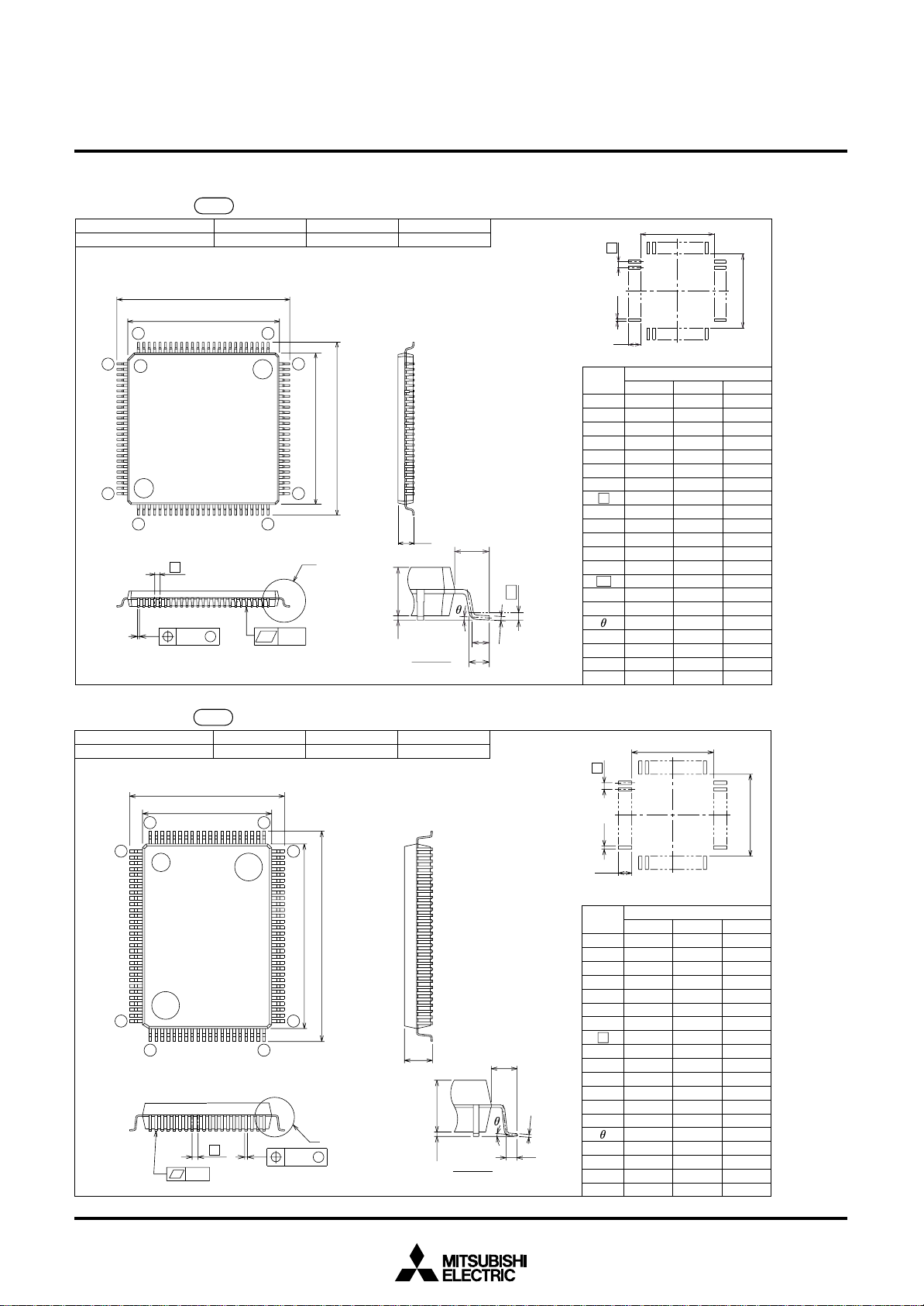
MITSUBISHI MICROCOMPUTERS
7560 Group
SINGLE-CHIP 8-BIT CMOS MICROCOMPUTER
PACKAGE OUTLINE
100P6Q-A
EIAJ Package Code
LQFP100-P-1414-0.50
100
1
25
b
MMP
JEDEC Code
H
D
D
e
x
M
Plastic 100pin 14✕14mm body LQFP
–
76
75
51
5026
0.63
E
E
H
F
y
Weight(g)
Lead Material
Cu Alloy
A
2
A
1
A
Detail F
M
D
e
E
2
b
l
2
M
Recommended Mount Pad
Symbol
L
1
A3
c
L
Lp
Dimension in Millimeters
Min Nom Max
–
A
0
A
1
––
2
A
b
c
D
E
e
–
D
H
E
H
L
L
1
––
Lp 0.45
A3
b
M
M
–
x
–
y
–
2
I
2
0.9
D
E
0.1
1.4
0.5
1.0
0.6
0.25
0.225
14.4
14.4
1.7
–
0.2
0.280.180.13
0.1750.1250.105
14.114.013.9
14.114.013.9
–
16.216.015.8
16.216.015.8
0.70.50.3
0.75
–
–
0.08
0.1
–
10°0°
–
––
––
––
––
100P6S-A
EIAJ Package Code
QFP100-P-1420-0.65 1.58
MMP
H
D
JEDEC Code
–
D
100
1
30
31
81
80
E
E
H
51
50
F
e
b
x
M
y
Weight(g)
Lead Material
Alloy 42
A
2
A
1
A
Detail F
Plastic 100pin 14✕20mm body QFP
D
M
e
E
2
b
I
2
Recommended Mount Pad
Symbol
Dimension in Millimeters
Min Nom Max
A
A
A
–
1
0
––
2
–
0.1
2.8
b
c
D
E
e
H
L
1
D
E
H
0.65
–
L
1.4
L
––
1
x ––0.13
c
y
–
–
–
b
L
2
I
2
1.3
M
D
M
E
0.35
14.6
20.6
M
3.05
0.2
0.40.30.25
0.20.150.13
14.214.013.8
20.220.019.8
–
17.116.816.5
23.122.822.5
0.80.60.4
0.1
10°0°
––
––
––
––
63

MITSUBISHI MICROCOMPUTERS
7560 Group
SINGLE-CHIP 8-BIT CMOS MICROCOMPUTER
HEAD OFFICE: 2-2-3, MARUNOUCHI, CHIYODA-KU, TOKYO 100-8310, JAPAN
Keep safety first in your circuit designs!
• Mitsubishi Electric Corporation puts the maximum effort into making semiconductor products better and more reliable, but there is always the possibility that trouble may occur with them. Trouble with semiconductors may lead to
personal injury, fire or property damage. Remember to give due consideration to safety when making your circuit designs, with appropriate measures such as (i) placement of substitutive, auxiliary circuits, (ii) use of non-flammable
material or (iii) prevention against any malfunction or mishap.
Notes regarding these materials
• These materials are intended as a reference to assist our customers in the selection of the Mitsubishi semiconductor product best suited to the customer’s application; they do not convey any license under any intellectual property
rights, or any other rights, belonging to Mitsubishi Electric Corporation or a third party.
• Mitsubishi Electric Corporation assumes no responsibility for any damage, or infringement of any third-party’s rights, originating in the use of any product data, diagrams, charts, programs, algorithms, or circuit application examples
contained in these materials.
• All information contained in these materials, including product data, diagrams, charts, programs and algorithms represents information on products at the time of publication of these materials, and are subject to change by
Mitsubishi Electric Corporation without notice due to product improvements or other reasons. It is therefore recommended that customers contact Mitsubishi Electric Corporation or an authorized Mitsubishi Semiconductor product
distributor for the latest product information before purchasing a product listed herein.
The information described here may contain technical inaccuracies or typographical errors. Mitsubishi Electric Corporation assumes no responsibility for any damage, liability, or other loss rising from these inaccuracies or errors.
Please also pay attention to information published by Mitsubishi Electric Corporation by various means, including the Mitsubishi Semiconductor home page (http://www.mitsubishichips.com).
• When using any or all of the information contained in these materials, including product data, diagrams, charts, programs, and algorithms, please be sure to evaluate all information as a total system before making a final decision
on the applicability of the information and products. Mitsubishi Electric Corporation assumes no responsibility for any damage, liability or other loss resulting from the information contained herein.
• Mitsubishi Electric Corporation semiconductors are not designed or manufactured for use in a device or system that is used under circumstances in which human life is potentially at stake. Please contact Mitsubishi Electric
Corporation or an authorized Mitsubishi Semiconductor product distributor when considering the use of a product contained herein for any specific purposes, such as apparatus or systems for transportation, vehicular, medical,
aerospace, nuclear, or undersea repeater use.
• The prior written approval of Mitsubishi Electric Corporation is necessary to reprint or reproduce in whole or in part these materials.
• If these products or technologies are subject to the Japanese export control restrictions, they must be exported under a license from the Japanese government and cannot be imported into a country other than the approved
destination.
Any diversion or reexport contrary to the export control laws and regulations of Japan and/or the country of destination is prohibited.
• Please contact Mitsubishi Electric Corporation or an authorized Mitsubishi Semiconductor product distributor for further details on these materials or the products contained therein.
© 2001 MITSUBISHI ELECTRIC CORP.
Specifications subject to change without notice.

REVISION HISTORY 7560 GROUP DATA SHEET
Rev. Date Description
Page Summary
1.0 03/28/01
1.1 06/08/01
First Edition
Table 13 VREF Min. VCC+0.3 → VCC52
(1/1)
 Loading...