

MITSUBISHI MICROCOMPUTERS
M37220M3-XXXSP
SINGLE-CHIP 8-BIT CMOS MICROCOMPUTER for VOLTAGE SYNTHESIZER
with ON-SCREEN DISPLAY CONTROLLER
DESCRIPTION
The M37220M3-XXXSP is a single-chip microcomputer designed with
CMOS silicon gate technology. It is housed in a 42-pin shrink plastic
molded DIP.
In addition to their simple instruction sets, the ROM, RAM and I/O
addresses are placed on the same memory map to enable easy programming.
The M37220M3-XXXSP has a PWM output function and a OSD display function, so it is useful for a channel selection system for TV.
FEATURES
Number of basic instructions .....................................................71
•
Memory size
•
The minimum instruction execution time
•
..........................................0.5µs (at 8 MHz oscillation frequency)
Power source voltage .................................................. 5 V ± 10 %
•
Power dissipation............................................................. 165 mW
•
(at 8 MHz oscillation frequency, V
Subroutine nesting ....................................... 96 levels (maximum)
•
Interrupts....................................................... 13 types, 13 vectors
•
8-bit timers .................................................................................. 4
•
Programmable I/O ports (Ports P0, P1, P2, P30–P32) ..............27
•
Input ports (Ports P33, P34)......................................................... 2
•
Output ports (Ports P52–P55) ......................................................4
•
12 V withstand ports ....................................................................6
•
LED drive ports ........................................................................... 4
•
Serial I/O ............................................................ 8-bit ✕ 1 channel
•
A-D comparator (6-bit resolution) ................................ 6 channels
•
D-A converter (6-bit resolution) ...................................................2
•
PWM output circuit......................................... 14-bit ✕ 1, 8-bit ✕ 6
•
ROM ........................................................12 K bytes
RAM ......................................................... 256 bytes
ROM for display......................................... 4 K bytes
RAM for display.......................................... 80 bytes
CC=5.5V, at CRT display)
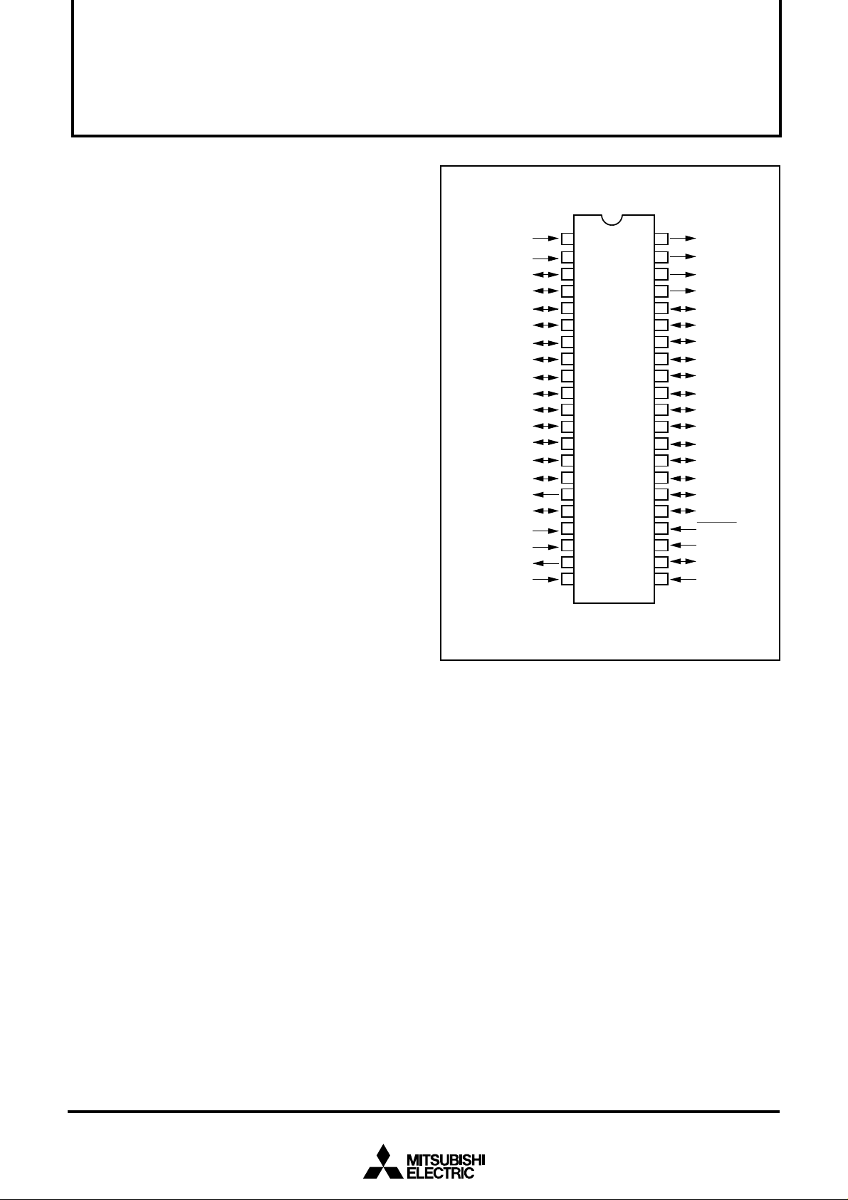
PIN CONFIGURATION (TOP VIEW)
HSYNC
VSYNC
P00/PWM0
P0
1/PWM1
P0
2/PWM2
P0
3/PWM3
P0
4/PWM4
P0
5/PWM5
P06/INT2/A-D4
P0
7/INT1
P2
3/TIM3
P2
4/TIM2
P2
P26
P27
D-A
P3
CNVSS
XIN
X
OUT
VSS
1
2
3
4
5
6
7
8
9
10
11
12
5
13
14
15
16
17
2
18
19
20
21
M37220M3-XXXSP
42
41
40
39
38
37
36
35
34
33
32
31
30
29
28
27
26
25
24
23
22
Outline 42P4B
P52/R
P5
3/G
P5
4/B
P5
5/OUT
P2
0/SCLK
P21/SOUT
P22/SIN
P10
P11
P12
P13
P14
P15/A-D1/INT3
P1
6/A-D2
P17/A-D3
0/A-D5/DA1
P3
P3
1/A-D6/DA2
RESET
OSC1/P3
3
OSC2/P34
VCC
CRT display function
•
Number of display characters ................24 characters ✕ 2 lines
(16 lines maximum)
Kinds of characters ..................................................... 128 kinds
Dot structure .......................................................... 12 ✕ 16 dots
Kinds of character sizes.................................................. 3 kinds
Kinds of character colors (It can be specified by the character)
maximum 7 kinds (R, G, B)
Kinds of raster colors (maximum 7 kinds)
Display position
Horizontal.................................................................. 64 levels
Vertical .................................................................... 128 levels
Bordering (horizontal and vertical)
APPLICATION
TV
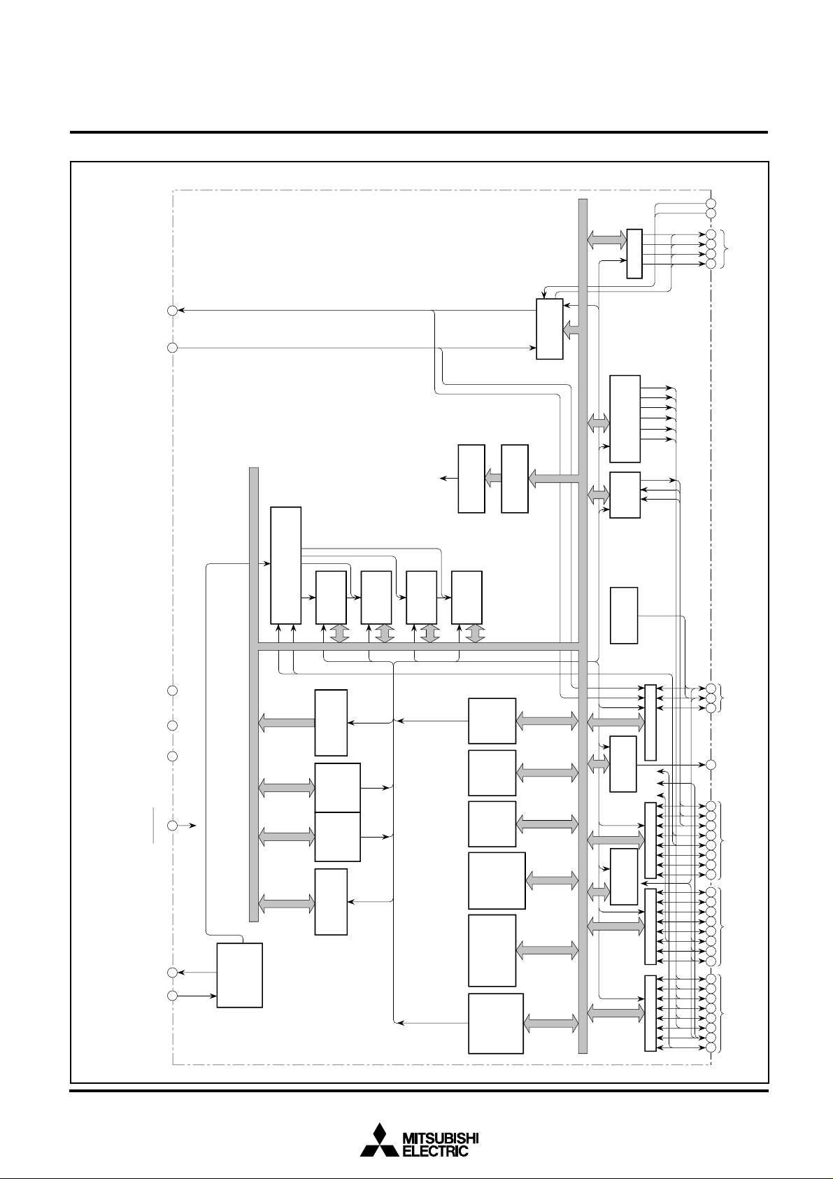
OUT
Clock input Clock output
X
IN
X
OUT
Reset input
V
CC
V
SS
CNV
SS
Clock output for display
Input ports P3
3,
P3
4
OSC1 OSC2
Clock input for display
INT2
INT1
PWM5
PWM4
PWM3
PWM2
PWM1
PWM0
P5 (4)
B
G
R
H
SYNC
V
SYNC
A-D
comparator
14-bit
PWM circuit
8-bit PWM circuit
Accumulator
A (8)
Timer 4
T4 (8)
Timer 3
T3 (8)
Timer 2
T2 (8)
Timer 1
T1 (8)
Timer count source
selection circuit
TIM2
TIM3
Instruction
register (8)
Instruction
decoder
Control signal
CRT circuit
Stack
pointer
S (8)
Index
register
Y (8)
Index
register
X (8)
Processor
status
register
PS (8)
8-bit
arithmetic
and
logical unit
ROM
12 K bytes
Program
counter
PC
L
(8)
Program
counter
PC
H
(8)
RAM
256 bytes
Data bus
Clock
generating
circuit
RESET
Output ports P5
2
–P5
5
Address bus
SI/O(8)
S
IN
S
CLK
S
OUT
INT3
10 9 8 7 6 5 4 3
I/O port P0
28 29 30 31 32 3334 35
P1 (8)
I/O port P1
15 14 13 12 11 3637 38
P2 (8)
I/O port P2
I/O ports P3
0
–P3
2
17 2627
16
P3 (3)
P0 (8)
39 40
41 42
2 1
2019
25
22
21 18
24 23
( φ ) Timing output
D-A
D-A
converter
MITSUBISHI MICROCOMPUTERS
M37220M3-XXXSP
SINGLE-CHIP 8-BIT CMOS MICROCOMPUTER for VOLTAGE SYNTHESIZER
with ON-SCREEN DISPLAY CONTROLLER
2
FUNCTIONAL BLOCK DIAGRAM of M37220M3-XXXSP
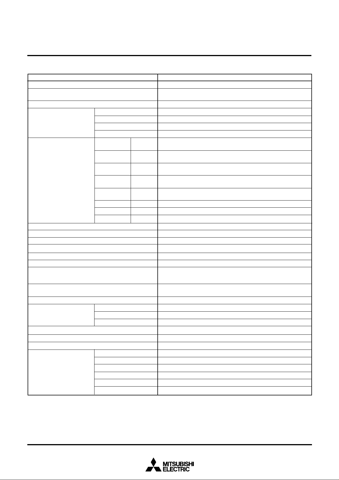
FUNCTIONS
Number of basic instructions
Instruction execution time
Clock frequency
Memory size
Input/Output ports
Serial I/O
A-D comparatpr
D-A converter
PWM output circuit
Timers
Subroutine nesting
Interrupt
Clock generating circuit
Power source voltage
Power dissipation
Operating temperature range
Device structure
Package
CRT display function
SINGLE-CHIP 8-BIT CMOS MICROCOMPUTER for VOLTAGE SYNTHESIZER
Parameter
ROM
RAM
CRT ROM
CRT RAM
P0
P10–P17
P20, P21
P22–P27
P30, P31
P32
P33, P34
P52–P55
CRT ON
CRT OFF
In stop mode
Number of display characters
Dot structure
Kinds of characters
Kinds of character sizes
Kinds of character colors
Display position (horizontal, vertical)
Input
Output
I/O
I/O
I/O
I/O
I/O
I/O
MITSUBISHI MICROCOMPUTERS
M37220M3-XXXSP
with ON-SCREEN DISPLAY CONTROLLER
Functions
71
0.5 µs (the minimum instruction execution time, at 8 MHz oscillation frequency)
8 MHz (maximum)
12K bytes
256 bytes
4K bytes
80 bytes
8-bit ✕ 1 (N-channel open-drain output structure, can be used as PWM
output pins, INT input pins, A-D input pin)
8-bit ✕ 1 (CMOS input/output structure, can be used as A-D input pins, INT
input pin)
2-bit ✕ 1 (CMOS input/output or N-channel open-drain output structure,
can be used as serial output pins)
6-bit ✕ 1 (CMOS input/output structure, can be used as serial input pin,
external clock input pins)
2-bit ✕ 1 (CMOS input/output or N-channel open-drain output structure,
can be used as A-D input pins, D-A conversion output pins)
1-bit ✕ 1 (N-channel open-drain output structure)
2-bit ✕ 1 (can be used as CRT display clock I/O pins)
4-bit ✕ 1 (CMOS output structure, can be used as CRT output pins)
8-bit ✕ 1
6 channels (6-bit resolution)
2 (6-bit resolution)
14-bit ✕ 1, 8-bit ✕ 6
8-bit timer ✕ 4
96 levels (maximum)
External interrupt ✕ 3, Internal timer interrupt ✕ 4, Serial I/O interrupt ✕ 1,
CRT interrupt ✕ 1, XIN/4096 interrupt ✕ 1, VSYNC interrupt ✕ 1,
BRK interrupt ✕ 1
2 built-in circuits (externally connected a ceramic resonator or a quartzcrystal oscillator)
5 V ± 10 %
165 mW typ. (at oscillation frequency fCPU = 8 MHz, fCRT = 8 MHz)
110 mW typ. (at oscillation frequency fCPU = 8 MHz)
1.65 mW (maximum)
–10 °C to 70 °C
CMOS silicon gate process
42-pin shrink plastic molded DIP
20 characters ✕ 2 lines (maximum 16 lines by software)
12 ✕ 16 dots
128 kinds
3 kinds
Maximum 7 kinds (R, G, B); can be specified by the character
64 levels (horizontal) ✕ 128 levels (vertical)
3
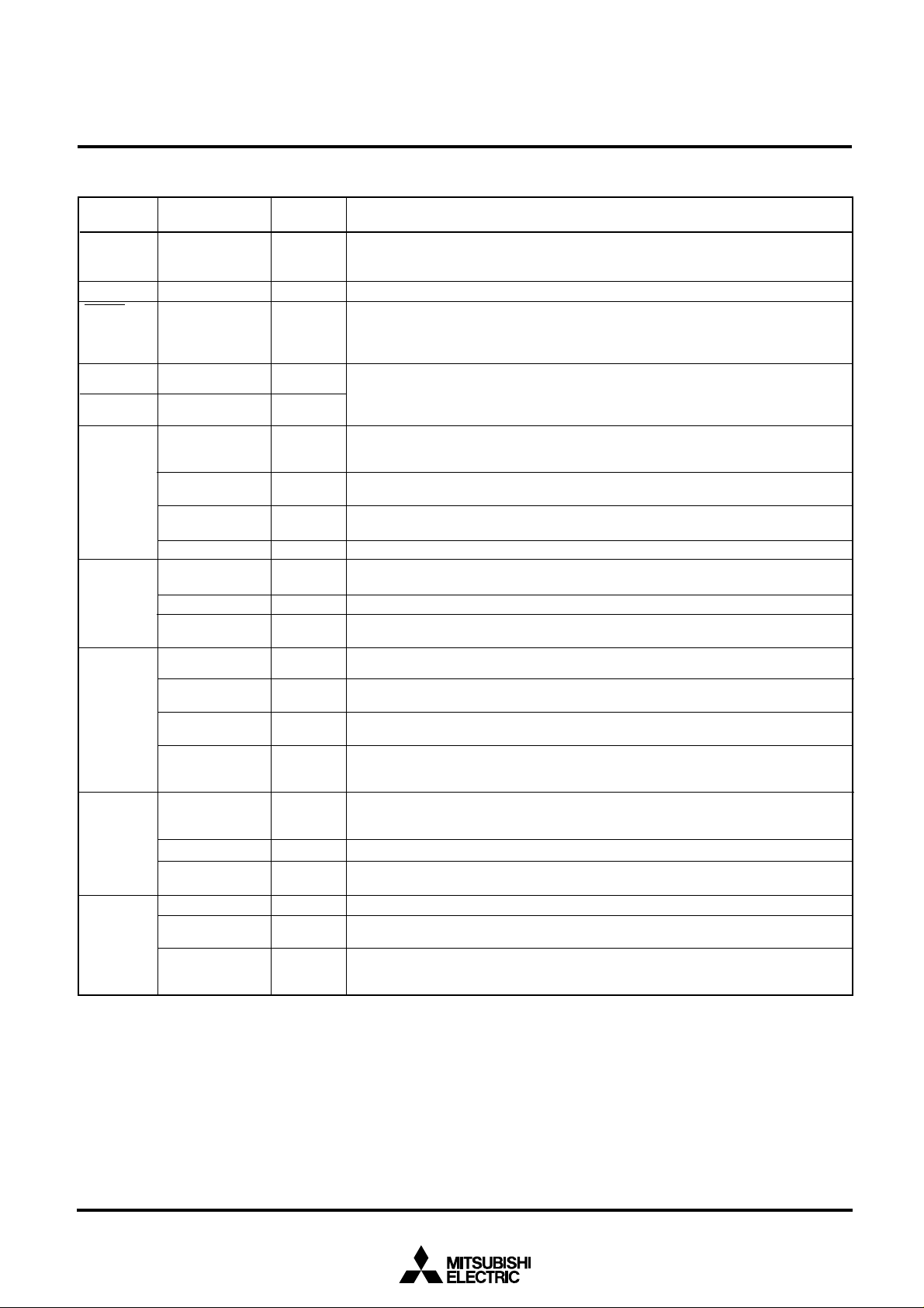
PIN DESCRIPTION
Pin
VCC, VSS
Name
Power source
Input/
Output
MITSUBISHI MICROCOMPUTERS
M37220M3-XXXSP
SINGLE-CHIP 8-BIT CMOS MICROCOMPUTER for VOLTAGE SYNTHESIZER
with ON-SCREEN DISPLAY CONTROLLER
Functions
Apply voltage of 5 V ± 10 % (typical) to VCC, and 0 V to VSS.
CNVSS
RESET
XIN
XOUT
P00/PWM0–
P05/PWM5,
P06/INT2/
A-D4,
P07/INT1
P10–P14,
P15/A-D1
INT3,
P16/A-D2,
P17/A-D3
P20/SCLK,
P2
1/SOUT,
P22/SIN,
P23/TIM3,
P24/TIM2,
P25–P27
P30/A-D5/
DA1,
P31/A-D6/
DA2,
P32
P33/OSC1,
P34/OSC2
SS
CNV
Reset input
Clock input
Clock output
I/O port P0
PWM output
External interrupt
input
Analog input
I/O port P1
Analog input
External interrupt
input
I/O port P2
External clock
input
Serial I/O data
input/output
Serial I/O synchronizing clock input/
output
I/O port P3
Analog input
D-A conversion
output
Input port P3
Clock input for
CRT display
Clock output for
CRT display
Input
Input
Output
I/O
Output
Input
Input
I/O
Input
Input
I/O
Input
I/O
I/O
I/O
Input
Output
Input
Input
Output
This is connected to VSS.
To enter the reset state, the reset input pin must be kept at a “L” for 2 µs or more (under
normal VCC conditions).
If more time is needed for the quartz-crystal oscillator to stabilize, this “L” condition should
be maintained for the required time.
This chip has an internal clock generating circuit. To control generating frequency, an
external ceramic resonator or a quartz-crystal oscillator is connected between pins XIN and
XOUT. If an external clock is used, the clock source should be connected to the XIN pin and
the XOUT pin should be left open.
Port P0 is an 8-bit I/O port with direction register allowing each I/O bit to be individually
programmed as input or output. At reset, this port is set to input mode. The output structure
is N-channel open-drain output. The note out of this Table gives a full of port P0 function.
Pins P00–P05 are also used as PWM output pins PWM0–PWM5 respectively.The output
structure is N-channel open-drain output.
Pins P06, P07 are also used as external interrupt input pins INT2, INT1 respectively.
Pins P06 is also used as an analog interrupt input pin A-D4.
Port P1 is an 8-bit I/O port and has basically the same functions as port P0. The output
structure is CMOS output.
Pins P15–P17 are also used as an analog input pins A-D1 to A-D3.
Pin P15 is also used as an external interrupt input pins INT3.
Port P2 is an 8-bit I/O port and has basically the same functions as port P0. The output
structure is CMOS output.
3, P24 is also used an external clock input pins TIM3, TIM2 respectively.
Pins P2
Pins P21, P22 are also used serial I/O data input/output pins SOUT, SIN respectively. The
output structure is N-channel open-drain output.
Pin P20 is also used serial I/O syncronizing clock input/output pin SCLK. The output structure is N-channel open-drain output.
Ports P30–P32 are a 3-bit I/O port and have basically the same functions as port P0. Either
CMOS output or N-channel open-drain output structure can be selected as the ports P30
and P31. The output structure of port P32 is N-channel open-drain output.
Pins P30, P31 are also used as analog input pins A-D5, A-D6 respectively.
Pins P30, P31 are also used as D-A conversion output pins DA1, DA2 respectively.
Ports P33, P34 are a 2-bit input port.
Pin P33 is also used as CRT display clock input pin OSC1.
4 is also used as CRT display clock output pin OSC2.The output structure is CMOS
Pin P3
output.
4
PIN DESCRIPTION (continued)
MITSUBISHI MICROCOMPUTERS
M37220M3-XXXSP
SINGLE-CHIP 8-BIT CMOS MICROCOMPUTER for VOLTAGE SYNTHESIZER
with ON-SCREEN DISPLAY CONTROLLER
P52/R,
P53/G,
P54/B,
P55/OUT
HSYNC
VSYNC
D-A
Note : As shown in the memory map (Figure 3), port P0 is accessed as a memory at address 00C016 of zero page. Port P0 has the port P0
direction register (address 00C1
programmed as “1” in the direction register are output pins. When pins are programmed as “0,” they are input pins. When pins are
programmed as output pins, the output data are written into the port latch and then output. When data is read from the output pins, the
output pin level is not read but the data of the port latch is read. This allows a previously-output value to be read correctly even if the
output “L” voltage has risen, for example, because a light emitting diode was directly driven. The input pins are in the floating state, so the
values of the pins can be read. When data is written into the input pin, it is written only into the port latch, while the pin remains in the
floating state.
Output port
P5
CRT output
SYNC input
H
VSYNC input
DA output
Output
Output
Output
Ports P52–P55 are a 4-bit output port. The output structure is CMOS output.
Pins P52–P55 are also used as CRT output pins R, G, B, OUT respectively. The output structure is
CMOS output.
This is a horizontal synchronizing signal input for CRT display.
Input
This is a vertical synchronizing signal input for CRT display.
Input
This is an output pin for 14-bit PWM.
16 of zero page) which can be used to program each bit as an input (“0”) or an output (“1”). The pins
5
MITSUBISHI MICROCOMPUTERS
M37220M3-XXXSP
SINGLE-CHIP 8-BIT CMOS MICROCOMPUTER for VOLTAGE SYNTHESIZER
with ON-SCREEN DISPLAY CONTROLLER
FUNCTIONAL DESCRIPTION
Central Processing Unit (CPU)
The M37220M3-XXXSP uses the standard 740 family instruction set.
Refer to the table of 740 family addressing modes and machine instructions or the SERIES 740 <Software> User’s Manual for details
on the instruction set.
Machine-resident 740 family instructions are as follows:
The FST, SLW instruction cannot be used.
The MUL, DIV, WIT and STP instruction can be used.
70
11111 00
CPU Mode Register
The CPU mode register contains the stack page selection bit. The
CPU mode register is allocated at address 00FB
CPU mode register
(CPUM : address 00FB16)
Fix these bits to “0.”
Stack page selection bit (Note)
0 : Zero page
1 : 1 page
16.
Fig. 1. Structure of CPU mode register
Fix these bits to “1.”
Note :
Please beware of this bit when programming because it
is set to “1” after the reset release.
6
MITSUBISHI MICROCOMPUTERS
M37220M3-XXXSP
SINGLE-CHIP 8-BIT CMOS MICROCOMPUTER for VOLTAGE SYNTHESIZER
with ON-SCREEN DISPLAY CONTROLLER
MEMORY
Special Function Register (SFR) Area
The special function register (SFR) area in the zero page contains
control registers such as I/O ports and timers.
RAM
RAM is used for data storage and for stack area of subroutine calls
and interrupts.
ROM
ROM is used for storing user programs as well as the interrupt vector
area.
RAM for Display
RAM for display is used for specifying the character codes and colors to display.
ROM for Display
ROM for display is used for storing character data.
0000
16
00C0
00FF
16
SFR area
16
RAM
(256 bytes)
Interrupt Vector Area
The interrupt vector area contains reset and interrupt vectors.
Zero Page
The 256 bytes from addresses 000016 to 00FF16 are called the zero
page area. The internal RAM and the special function registers (SFR)
are allocated to this area.
The zero page addressing mode can be used to specify memory and
register addresses in the zero page area. Access to this area with
only 2 bytes is possible in the zero page addressing mode.
Special Page
The 256 bytes from addresses FF0016 to FFFF16 are called the special page area. The special page addressing mode can be used to
specify memory addresses in the special page area. Access to this
area with only 2 bytes is possible in the special page addressing
mode.
16
10000
ROM
Zero page
for display
(4 K bytes)
10FFF
16
RAM
for display (Note)
(80 bytes)
ROM
(12 K bytes)
Fig. 2. Memory map
013F
16
Not used
0600
16
06B3
16
Not used
D000
16
FF00
16
FFDE
16
Interrupt vector area
16
FFFF
Note : Refer to Table 8. Contents of CRT display RAM.
Special page
1FFFF
Not used
16
7
SINGLE-CHIP 8-BIT CMOS MICROCOMPUTER for VOLTAGE SYNTHESIZER
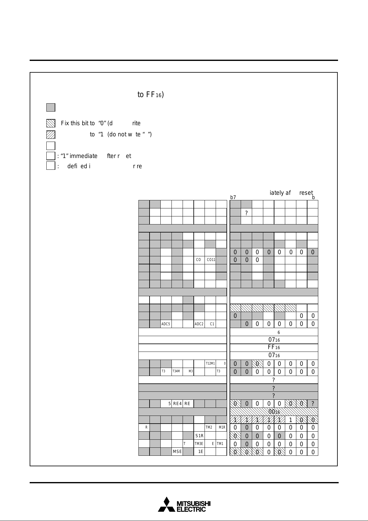
■SFR area (addresses C016 to DF16)
: Nothing is allocated
: Fix this bit to “0” (do not write “1”)
: “0” immediately after reset
0
1
: “1” immediately after reset
?
: undefined immediately after reset
MITSUBISHI MICROCOMPUTERS
M37220M3-XXXSP
with ON-SCREEN DISPLAY CONTROLLER
Address
Port P0 (P0)
C0
16
Port P0 direction register (D0)
C1
16
Port P1 (P1)
C2
16
Port P1 direction register (D1)
C3
16
Port P2 (P2)
C4
16
Port P2 direction register (D2)
C5
16
Port P3 (P3)
C6
16
Port P3 direction register (D3)
C7
16
C8
16
C9
16
Port P5 (P5)
CA
16
Port P5 direction register (D5)
CB
16
CC
16
Port P3 output mode control register (P3S)
CD
16
DA-H register (DA-H)
CE
16
DA-L register (DA-L)
CF
16
PWM0 register (PWM0)
D0
16
PWM1 register (PWM1)
D1
16
PWM2 register (PWM2)
D2
16
PWM3 register (PWM3)
D3
16
PWM4 register (PWM4)
D4
16
PWM output control register 1 (PW)
D5
16
PWM output control register 2 (PN)
D6
16
D7
16
D8
16
D9
16
DA
16
DB
16
Serial I/O mode register (SM)
DC
16
Serial I/O regsiter (SIO)
DD
16
DA1 conversion register (DA1)
DE
16
DA2 conversion register (DA2)
DF
16
Register
b7
Bit allocation
DA1SDA2S
PN2PN3PN4
State immediately after reset
b0
b7
00
00
00
000
00000000
00
00000000
P30SP31S
00000000
00
PW0PW1PW2PW3PW4PW5PW6PW7
00
00000000
SM0SM1SM2SM3SM5SM6
DA10DA11DA12DA13DA14DA15
DA20DA21DA22DA23DA24DA25
00000000
?00 ?????
?00 ?????
?
16
?
16
?
16
?????
?
?
?
?
????
?
?
??????
?
?
?
?
?
16
?
?
?
?
?
?
b0
Fig. 3. Memory map of SFR (special function register) (1)
8
SINGLE-CHIP 8-BIT CMOS MICROCOMPUTER for VOLTAGE SYNTHESIZER
A
A
AA
AA
AA
AA
AA
AA
AA
AA
AA
AA
A
AA
A
AA
A
AA
A
AA
A
AA
A
AA
A
AA
AA
AA
AAAAAAAAAAAA
AA
AA
AA
AA
AA
■SFR area (addresses E016 to FF16)
: Nothing is allocated
: Fix this bit to “0” (do not write “1”)
: Fix this bit to “1” (do not write “0”)
: “0” immediately after reset
0
1
: “1” immediately after reset
?
: undefined immediately after reset
MITSUBISHI MICROCOMPUTERS
M37220M3-XXXSP
with ON-SCREEN DISPLAY CONTROLLER
Address
Horizontal position register (HR)
E016
Vertical register 1 (CV1)
E116
Vertical register 2 (CV2)
E216
Register
E316
Character size register (CS)
E416
Border selection register (MD)
E516
Color register 0 (CO0)
E616
Color register 1 (CO1)
E716
Color register 2 (CO2)
E816
Color register 3 (CO3)
E916
CRT control register (CC)
EA16
EB16
CRT port control register (CRTP)
EC16
CRT clock selection register (CK)
ED16
A-D control register 1 (AD1)
EE16
A-D control register 2 (AD2)
EF16
Timer 1 (TM1)
F016
Timer 2 (TM2)
F116
Timer 3 (TM3)
F216
Timer 4 (TM4)
F316
Timer 12 mode register (T12M)
F416
Timer 34 mode register (T34M)
F516
PWM5 register (PWM5)
F616
F716
F816
Interrupt input polarity register (RE)
F916
Test register (TEST)
FA16
CPU mode register (CPUM)
FB16
Interrupt request register 1 (IREQ1)
FC16
Interrupt request register 2 (IREQ2)
FD16
Interrupt control register 1 (ICON1)
FE16
Interrupt control register 2 (ICON2)
FF16
b7
Bit allocation
OUTOP5OP6OP7
A
T34M5
A
CK0RE5 RE4 RE3
CK0
MSR
A
A
ADC2ADC4 ADC3ADC5
CM2
S1R
S1EMSE
State immediately after reset
b0
b7
HR0HR1HR2HR3HR4HR5
00000000
CV10CV11CV12CV13CV14CV15CV16
0
CV20CV21CV22CV23CV24CV25CV26
??????
?
?0??????
b0
?
CS10CS11CS20CS21
0000
MD10MD20
00000 0
CO01CO02CO03CO05
CO11CO12CO13CO15
CO21CO22CO23CO25
CO31CO32CO33CO35
00000 00 0
00000 00 0
00000 00 0
00000 00 0
CC0CC1CC2
00000000
????
??
?
VSYCR/G/B
HSYC
CK0CK1
ADM0ADM1ADM2ADM4
ADC0ADC1
000000 0
0
00 00000
000000 00
A
0016
?
FF
A
16
0716
FF16
0716
T12M0
T12M1T12M2T12M3T12M4
T34M0
T34M1T34M2T34M3T34M4
000000 00
000000 00
?
?
?
11
A
A
CK0
00
CK0
16
A
A
1
0
1
0?
00
A
0000
0
1
1
TM1R
TM2RTM3RTM4RCRTRVSCRIT3R
1T1R1T2R
TM1E
TM2ETM3ETM4ECRTEVSCEIT3E
1T1E1T2E
0000 0000
0000 00
00
A
0000 0000
A
0000 0000
A
A
Fig. 4. Memory map of SFR (special function register) (2)
9
MITSUBISHI MICROCOMPUTERS
M37220M3-XXXSP
SINGLE-CHIP 8-BIT CMOS MICROCOMPUTER for VOLTAGE SYNTHESIZER
with ON-SCREEN DISPLAY CONTROLLER
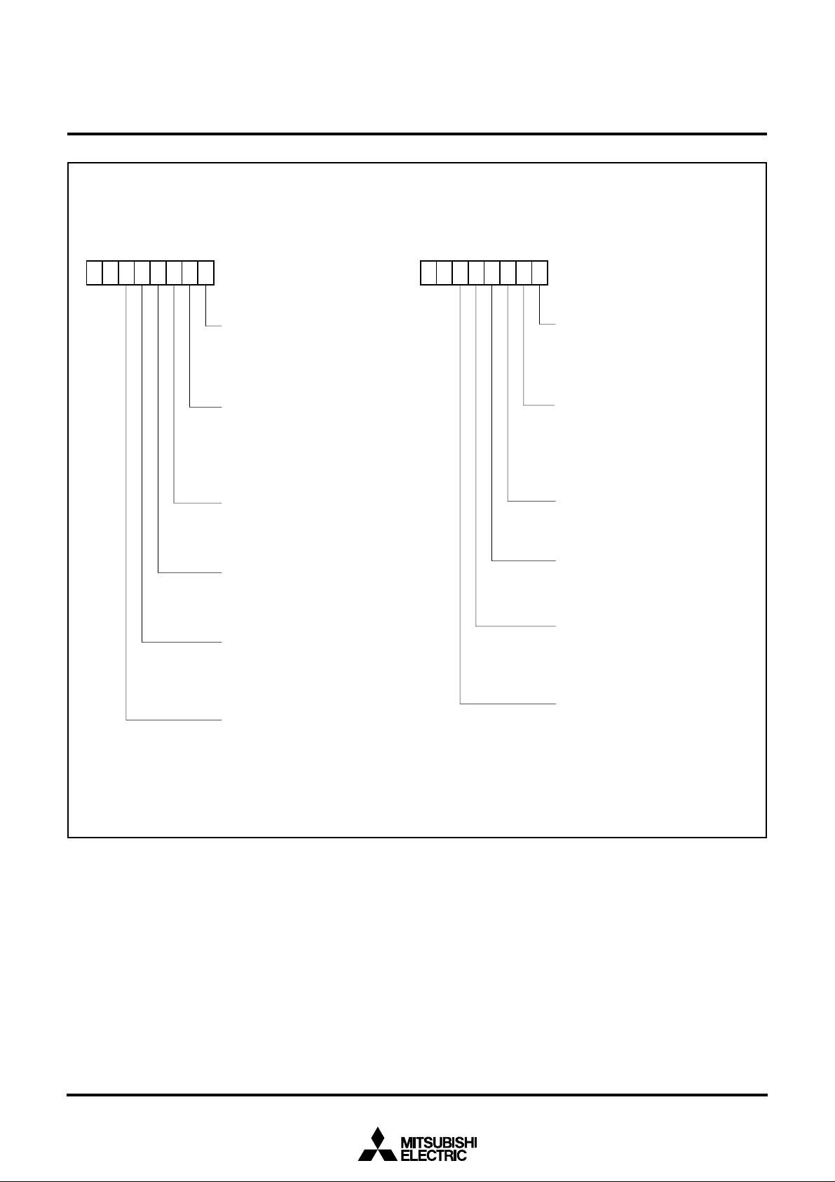
INTERRUPTS
Interrupts can be caused by 13 different sources consisting of 3 external, 9 internal, and 1 software sources. Interrupts are vectored
interrupts with priorities shown in Table 1. Reset is also included in
the table because its operation is similar to an interrupt.
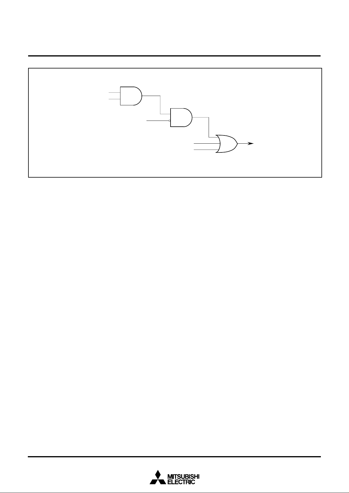
When an interrupt is accepted,
(1) The contents of the program counter and processor status
register are automatically stored into the stack.
(2) The interrupt disable flag I is set to “1” and the corresponding
interrupt request bit is set to “0.”
(3) The jump destination address stored in the vector address enters
the program counter.
Other interrupts are disabled when the interrupt disable flag is set to
“1.”
All interrupts except the BRK instruction interrupt have an interrupt
request bit and an interrupt enable bit. The interrupt request bits are
in interrupt request registers 1 and 2 and the interrupt enable bits are
in interrupt control registers 1 and 2. Figure 5 shows the structure of
the interrupt-related registers.
Interrupts other than the BRK instruction interrupt and reset are accepted when the interrupt enable bit is “1,” interrupt request bit is “1,”
and the interrupt disable flag is “0.” The interrupt request bit can be
set to “0” by a program, but not set to “1.” The interrupt enable bit can
be set to “0” and “1” by a program.
Reset is treated as a non-maskable interrupt with the highest priority.
Figure 6 shows interrupt control.
Interrupt Causes
(1) VSYNC and CRT interrupts
The V
SYNC interrupt is an interrupt request synchronized with
the vertical sync signal.
The CRT interrupt occurs after character block display to the CRT
is completed.
(2) INT1, INT2, INT3 interrupts
With an external interrupt input, the system detects that the level
of a pin changes from “L” to “H” or from “H” to “L,” and generates
an interrupt request. The input active edge can be selected by
bits 3, 4 and 5 of the interrupt input polarity register (address
00F9
16) : when this bit is “0,” a change from “L” to “H” is de-
tected; when it is “1,” a change from “H” to “L” is detected. Note
that all bits are cleared to “0” at reset.
(3) Timer 1, 2, 3 and 4 interrupts
An interrupt is generated by an overflow of timer 1, 2, 3 or 4.
(4) Serial I/O interrupt
This is an interrupt request from the clock synchronous serial
I/O function.
(5) X
IN/4096 interrupt
This interrupt occurs regularly with a f(X
of the PWM output control register 1 to “0.”
(6) BRK instruction interrupt
This software interrupt has the least significant priority. It does
not have a corresponding interrupt enable bit, and it is not affected by the interrupt disable flag I (non-maskable).
IN)/4096 period. Set bit 0
Table 1. Interrupt vector addresses and priority
Interrupt source
Reset
CRT interrupt
INT2 interrupt
INT1 interrupt
Timer 4 interrupt
XIN/4096 interrupt
VSYNC interrupt
Timer 3 interrupt
Timer 2 interrupt
Timer 1 interrupt
Serial I/O interrupt
INT3 interrupt
BRK instruction interrupt
Priority
1
2
3
4
5
6
7
8
9
10
11
12
13
Vector addresses
FFFF16, FFFE16
FFFD16, FFFC16
FFFB16, FFFA16
FFF916, FFF816
FFF516, FFF416
FFF316, FFF216
FFF116, FFF016
FFEF16, FFEE16
FFED16, FFEC16
FFEB16, FFEA16
FFE916, FFE816
FFE516, FFE416
FFDF16, FFDE16
Remarks
Non-maskable
Active edge selectable
Active edge selectable
Active edge selectable
Non-maskable (software interrupt)
10
MITSUBISHI MICROCOMPUTERS
M37220M3-XXXSP
SINGLE-CHIP 8-BIT CMOS MICROCOMPUTER for VOLTAGE SYNTHESIZER
with ON-SCREEN DISPLAY CONTROLLER
7
7
0
Interrupt request register 1
(IREQ1 : address 00FC
Timer 1 interrupt request bit
Timer 2 interrupt request bit
Timer 3 interrupt request bit
Timer 4 interrupt request bit
CRT interrupt request bit
V
SYNC
interrupt request bit
INT3 interrupt request bit
0
Interrupt control register 1
(ICON1 : address 00FE
Timer 1 interrupt enable bit
Timer 2 interrupt enable bit
Timer 3 interrupt enable bit
Timer 4 interrupt enable bit
CRT interrupt enable bit
V
SYNC
interrupt enable bit
INT3 interrupt enable bit
7
16
)
0
0 : No interrupt request issued
1 : Interrupt request issued
7
0
16
)
00 0
0
Interrupt request register 2
(IREQ2 : address 00FD
INT1 interrupt request bit
INT2 interrupt request bit
Serial I/O interrupt request bit
XIN/4096 interrupt request bit
Fix this bit to “0.”
0
Interrupt control register 2
(ICON2 : address 00FF
INT1 interrupt enable bit
INT2 interrupt enable bit
Serial I/O interrupt enable bit
Fix this bit to “0.”
XIN/4096 interrupt enable bit
Fix these bits to “0.”
16
)
16
)
7 0
00
Interrupt input polarity register
0
(RE : address 00F9
Fix these bits to “0.”
INT1 polarity switch bit
0 : Positive polarity
1 : Negative polarity
INT2 polarity switch bit
0 : Positive polarity
1 : Negative polarity
INT3 polarity switch bit
0 : Positive polarity
1 : Negative polarity
Fix this bit to “0.”
Fig. 5. Structure of interrupt-related registers
0 : Interrupt disabled
1 : Interrupt enabled
16
)
11
Interrupt request bit
Interrupt enable bit
Interrupt disable flag I
MITSUBISHI MICROCOMPUTERS
M37220M3-XXXSP
SINGLE-CHIP 8-BIT CMOS MICROCOMPUTER for VOLTAGE SYNTHESIZER
with ON-SCREEN DISPLAY CONTROLLER
Fig. 6. Interrupt control
BRK instruction
Reset
Interrupt request
12

MITSUBISHI MICROCOMPUTERS
M37220M3-XXXSP
SINGLE-CHIP 8-BIT CMOS MICROCOMPUTER for VOLTAGE SYNTHESIZER
with ON-SCREEN DISPLAY CONTROLLER
TIMERS
The M37220M3-XXXSP has 4 timers: timer 1, timer 2, timer 3, and
timer 4. All timers are 8-bit timers with the 8-bit timer latch. The timer
block diagram is shown in Figure 8.
All of the timers count down and their divide ratio is 1/(n+1), where n
is the value of timer latch. The value is set to a timer at the same time
by writing a count value to the corresponding timer latch (addresses
00F0
16 to 00F316).
The count value is decremented by 1. The timer interrupt request bit
is set to “1” by a timer overflow at the next count pulse after the count
value reaches “00
16”.
(1) Timer 1
Timer 1 can select one of the following count sources:
f(XIN)/16
•
f(XIN)/4096
•
The count source of timer 1 is selected by setting bit 0 of the timer 12
mode register (address 00F4
Timer 1 interrupt request occurs at timer 1 overflow.
16).
(2) Timer 2
Timer 2 can select one of the following count sources:
f(XIN)/16
•
Timer 1 overflow signal
•
External clock from the P24/TIM2 pin
•
The count source of timer 2 is selected by setting bits 4 and 1 of the
timer 12 mode register (address 00F4
signal is a count source for the timer 2, the timer 1 functions as an 8bit prescaler.
Timer 2 interrupt request occurs at timer 2 overflow.
16). When timer 1 overflow
At reset, timers 3 and 4 are connected by hardware and “FF
automatically set in timer 3; “07
lected as the timer 3 count source. The internal reset is released by
timer 4 overflow at these state, the internal clock is connected.
At execution of the STP instruction, timers 3 and 4 are connected by
hardware and “FF
However, the f(X
So set bit 0 of the timer 34 mode register (address 00F5
before the execution of the STP instruction (f(X
the timer 3 count source). The internal STP state is released by timer
4 overflow at these state, the internal clock is connected.
Because of this, the program starts with the stable clock.
The structure of timer-related registers is shown in Figure 7.
16” is automatically set in timer 3; “0716” in timer 4.
IN)/16 is not selected as the timer 3 count source.
16” in timer 4. The f(XIN)/16 is se-
IN)/16 is selected as
16” is
16) to “0”
(3) Timer 3
Timer 3 can select one of the following count sources:
f(XIN)/16
•
External clock from the HSYNC pin
•
External clock from the P23/TIM3 pin
•
The count source of timer 3 is selected by setting bits 5 and 0 of the
timer 34 mode register (address 00F5
Timer 3 interrupt request occurs at timer 3 overflow.
16)
(4) Timer 4
Timer 4 can select one of the following count sources:
f(XIN)/16
•
f(XIN)/2
•
Timer 3 overflow signal
•
The count source of timer 3 is selected by setting bits 4 and 1 of the
timer 34 mode register (address 00F5
signal is a count source for the timer 4, the timer 3 functions as an 8bit prescaler.
Timer 4 interrupt request occurs at timer 4 overflow.
16). When timer 3 overflow
13
MITSUBISHI MICROCOMPUTERS
M37220M3-XXXSP
SINGLE-CHIP 8-BIT CMOS MICROCOMPUTER for VOLTAGE SYNTHESIZER
with ON-SCREEN DISPLAY CONTROLLER
70
0
Timer 12 mode register
(T12M : address 00F416)
Timer 1 count source selection bit
0 : f(XIN)/16
1 : f(XIN)/4096
Timer 2 count source selection bit
0 : Internal clock
1 : External clock from P2
Timer 1 count stop bit
0 : Count start
1 : Count stop
Timer 2 count stop bit
0 : Count start
1 : Count stop
Timer 2 internal count source
selection bit
0 : f(XIN)/16
1 : Timer 1 overflow
4/TIM2 pin
70
Timer 34 mode register
(T34M : address 00F516)
Timer 3 count source selection bit
0 : f(X
1 : External clock
Timer 4 internal count source
selection bit
0 : Timer 3 overflow
1 : f(X
Timer 3 count stop bit
0 : Count start
1 : Count stop
Timer 4 count stop bit
0 : Count start
1 : Count stop
Timer 4 count source selection bit
0 : Internal clock
1 : f(X
IN)/16
IN)/16
IN)/2
Fix this bit to “0.”
Fig. 7. Structure of timer-related registers
Timer 3 external count source
selection bit
0 : External clock from P2
1 : External clock from HSYNC pin
3/TIM3 pin
14
MITSUBISHI MICROCOMPUTERS
M37220M3-XXXSP
SINGLE-CHIP 8-BIT CMOS MICROCOMPUTER for VOLTAGE SYNTHESIZER
with ON-SCREEN DISPLAY CONTROLLER
Data bus
8
X
P24/TIM2
H
SYNC
3
/TIM3
P2
1/4096
IN
1/2
1/8
T12M0
T12M4
T12M1
T34M0
T12M2
T12M3
T34M5
T34M2
Timer 1 latch (8)
8
Timer 1 (8)
Timer 2 latch (8)
8
Timer 2 (8)
Timer 3 latch (8)
8
Timer 3 (8)
Timer 1
interrupt request
8
8
Timer 2
interrupt request
8
8
FF
16
8
Reset
STP
instruction
Timer 3
interrupt request
Selection gate :
Connected to black
colored side at reset
T12M : Timer 12 mode register
T34M : Timer 34 mode register
Notes 1 : “H” pulse width of external clock inputs TIM2 and TIM3 needs 4 machine cycles or more.
2 :
When the external clock source is selected, timers 2 and 3 are counted at a rising edge
of input signal.
3 :In the stop mode or the wait mode, external clock inputs TIM2 and TIM3 cannot be used
T34M1
Timer 4 latch (8)
Timer 4 (8)
T34M4
T34M3
Fig. 8. Timer block diagram
8
07
16
8
Timer 4
interrupt request
8
15
SINGLE-CHIP 8-BIT CMOS MICROCOMPUTER for VOLTAGE SYNTHESIZER
SERIAL I/O
The M37220M3-XXXSP has a built-in serial I/O which can either transmit or receive 8-bit data in serial in the clock synchronous mode.
The serial I/O block diagram is shown in Figure 9. The synchronizing
clock I/O pin (S
port P2.
Bit 2 of the serial I/O mode register (address 00DC
the synchronizing clock is supplied internally or externally (from the
P2
0/SCLK pin). When an internal clock is selected, bits 1 and 0 select
whether f(X
port P2 is used for serial I/O or not. To use the P2
pin, set the bit 2 of the port P2 direction register (address 00C516) to
“0.”
The operation of the serial I/O function is described below. The function of the serial I/O differs depending on the clock source; external
clock or internal clock.
CLK), and data I/O pins (SOUT, SIN) also function as
16) selects whether
IN) is divided by 4, 16, 32, or 64. Bit 3 selects whether
2/SIN pin as the SIN
MITSUBISHI MICROCOMPUTERS
M37220M3-XXXSP
with ON-SCREEN DISPLAY CONTROLLER
IN
X
P2
1/2
0 latch
P20/SCLK
SM3
1 latch
P2
P21/SOUT
SM3
P22/SIN
Note: When the data is set in the serial I/O register (address 00DD
Fig. 9. Serial I/O block diagram
1/2
Synchronization circuit
SM5: LSB
SM6
Frequency
divider
SM2
S
Serial I/O counter (8)
MSB
(Note)
Serial I/O shift register (8)
(Address 00DD16)
16), the register functions as the serial I/O shift register.
1/81/4 1/16
SM1
SM0
8
Data bus
Selection gate :
Connected to black
colored side at reset.
SM : Serial I/O mode register
Serial I/O interrupt
request
16

SINGLE-CHIP 8-BIT CMOS MICROCOMPUTER for VOLTAGE SYNTHESIZER
Internal clock—the serial I/O counter is set to “7” during write cycle
into the serial I/O register (address 00DD
“H” forcibly. At each falling edge of the transfer clock after the write
cycle, serial data is output from the S
be selected by bit 5 of the serial I/O mode register. At each rising
edge of the transfer clock, data is input from the S
the serial I/O register is shifted 1 bit.
After the transfer clock has counted 8 times, the serial I/O counter
becomes “0” and the transfer clock stops at “H.” At this time the interrupt request bit is set to “1.”
External clock—when an external clock is selected as the clock
source, the interrupt request is set to “1” after the transfer clock has
counted 8 times. However, transfer operation does not stop, so control the clock externally. Use the external clock of 1MHz or less with
a duty cycle of 50%.
The serial I/O timing is shown in Figure 11. When using an external
clock for transfer, the external clock must be held at “H” for initializing
the serial I/O counter. When switching between an internal clock and
an external clock, do not switch during transfer. Also, be sure to initialize the serial I/O counter after switching.
16), and transfer clock goes
OUT pin. Transfer direction can
IN pin and data in
MITSUBISHI MICROCOMPUTERS
M37220M3-XXXSP
with ON-SCREEN DISPLAY CONTROLLER
7
0
0
Serial I/O mode register
(SM : address 00DC
Internal synchronizing clock
selection bits
b1 b0
0 0 : f(XIN)/4
0 1 : f(XIN)/16
1 0 : f(XIN)/32
1 1 : f(XIN)/64
Synchronizing clock selection bit
0 : External clock
1 : Internal clock
Serial I/O port selection bit
0 : P20, P21 functions as port
1 : SCLK, SOUT
Fix this bit to “0.”
16)
Notes 1: On programming, note that the serial I/O counter is set by
writing to the serial I/O register with the bit managing instructions as SEB and CLB instructions.
2: When an external clock is used as the synchronizing clock,
write transmit data to the serial I/O register at “H” of the
transfer clock input level.
Synchroninzing clock
Transfer clock
Serial I/O register
write signal
Serial I/O output
Serial I/O input
S
SOUT
IN
D0 D1 D2 D3 D4 D5 D6 D7
Transfer direction selection bit
0 : LSB first
1 : MSB first
Serial input pin selection bit
0 : Input signal from SIN pin
1 : Input signal from SOUT pin
Fig. 10. Structure of serial I/O mode register
(Note)
Note : When an internal clock is selected, the S
Fig. 11. Serial I/O timing (for LSB first)
Interrupt request bit is set to “1”
OUT pin is at high-impedance after transfer is completed.
17

SINGLE-CHIP 8-BIT CMOS MICROCOMPUTER for VOLTAGE SYNTHESIZER
Serial I/O Common Transmission/Reception Mode
By writing “1” to bit 6 of the serial I/O mode register, signals SIN and
S
OUT are switched internally to be able to transmit or receive the
serial data.
Figure 12 shows signals on serial I/O common transmission/reception mode.
MITSUBISHI MICROCOMPUTERS
M37220M3-XXXSP
with ON-SCREEN DISPLAY CONTROLLER
Note: When receiving the serial data after writing “FF
I/O register.
P20/SCLK
P21/SOUT
P22/SIN
SM: Serial I/O mode register
Fig. 12. Signals on serial I/O common transmission/reception mode
16” to the serial
Clock
“1”
Serial I/O shift register (8)
“0”
SM6
18

MITSUBISHI MICROCOMPUTERS
M37220M3-XXXSP
SINGLE-CHIP 8-BIT CMOS MICROCOMPUTER for VOLTAGE SYNTHESIZER
with ON-SCREEN DISPLAY CONTROLLER
PWM OUTPUT FUNCTION
The M37220M3-XXXSP is equipped with a 14-bit PWM (DA) and six
8-bit PWMs (PWM0–PWM5). DA has a 14-bit resolution with the
minimum resolution bit width of 0.25µs (for f(X
IN) = 8 MHz) and a
repeat period of 4096µs. PWM0–PWM5 have the same circuit structure and an 8-bit resolution with minimum resolution bit width of 4µs
(for f(X
IN) = 8 MHz) and repeat period of 1024µs.
Figure 13 shows the PWM block diagram. The PWM timing generating circuit applies individual control signals to PWM0–PWM5 using
f(X
IN) divided by 2 as a reference signal.
(1) Data Setting
When outputting DA, first set the high-order 8 bits to the DA-H register (address 00CE
(address 00CF
data in the PWMi register (i means 0 to 5; addresses 00D0
00D4
16, 00F616).
16), then the low-order 6 bits to the DA-L register
16). When outputting PWM0–PWM5, set 8-bit output
16 to
(2) Transmitting Data from Register to PWM circuit
Data transfer from the 8-bit PWM register to 8-bit PWM circuit is
executed at writing data to the register.
The signal output from the 8-bit PWM output pin corresponds to the
contents of this register.
Also, data transfer from the DA register (addresses 00CE
00CF
16) to the 14-bit PWM circuit is executed at writing data to the
DA-L register (address 00CF
(address 00CE
16) means reading this transferred data. Accordingly,
16). Reading from the DA-H register
it is possible to confirm the data being output from the D-A output pin
by reading the DA register.
16 and
(4) Operating of 14-bit PWM
As with 8-bit PWM, set the bit 0 of the PWM output control register 1
(address 00D5
16) to “0” (at reset, bit 0 is already set to “0” automati-
cally), so that the PWM count source is supplied. Next, select the
output polarity by bit 2 of the PWM output control register 2 (address
00D6
16). Then, the 14-bit PWM outputs from the D-A output pin by
setting bit 1 of the PWM output control register 1 to “0” (at reset, this
bit already set to “0” automatically) to select the DA output.
The output example of the 14-bit PWM is shown in Figure 15.
The 14-bit PWM divides the data of the DA latch into the low-order 6
bits and the high-order 8 bits.
The fundamental waveform is determined with the high-order 8-bit
data “D
H.” A “H” level area with a length τ ✕ DH(“H” level area of
fundamental waveform) is output every short area of “t” = 256τ =
64µs (τ is the minimum resolution bit width of 0.25µs). The “H” level
area increase interval (t
“D
L.” The “H” level are of smaller intervals “tm” shown in Table 2 is
m) is determined with the low-order 6-bit data
longer by τ than that of other smaller intervals in PWM repeat period
“T” = 64t. Thus, a rectangular waveform with the different “H” width is
output from the D-A pin. Accordingly, the PWM output changes by τ
unit pulse width by changing the contents of the DA-H and DA-L
registers. A length of entirely “H” output cannot be output, i. e. 256/
256.
(5) Output after Reset
At reset, the output of port P00–P05 is in the high-impedance state,
and the contents of the PWM register and the PWM circuit are undefined. Note that after reset, the PWM output is undefined until setting
the PWM register.
(3) Operating of 8-bit PWM
The following is the explanation about PWM operation.
At first, set the bit 0 of PWM output control register 1 (address 00D5
to “0” (at reset, bit 0 is already set to “0” automatically), so that the
PWM count source is supplied.
PWM0–PWM5 are also used as pins P0
0–P05 respectively. For
PWM0–PWM5, set the corresponding bits of the port P0 direction
register to “1” (output mode). And select each output polarity by bit 3
of the PWM output control register 2(address 00D6
16). Then, set
bits 2 to 7 of the PWM output control register 1 to “1” (PWM output).
The PWM waveform is output from the PWM output pins by setting
these registers.
Figure 14 shows the 8-bit PWM timing. One cycle (T) is composed
of 256 (2
8
) segments. The 8 kinds of pulses relative to the weight of
each bit (bits 0 to 7) are output inside the circuit during 1 cycle. Refer
to Figure 14 (a). The 8-bit PWM outputs waveform which is the logical sum (OR) of pulses corresponding to the contents of bits 0 to 7 of
the 8-bit PWM register. Several examples are shown in Figure 14
(b). 256 kinds of output (“H” level area: 0/256 to 255/256) are selected by changing the contents of the PWM register. A length of
entirely “H” output cannot be output, i.e. 256/256.
16)
19

SINGLE-CHIP 8-BIT CMOS MICROCOMPUTER for VOLTAGE SYNTHESIZER
Table 2. Relation between the low-order 6-bit data and high-level
area increase interval
Low-order 6 bits of data
0 0 0 0 0 0
0 0 0 0 0 1
0 0 0 0 1 0
0 0 0 1 0 0
0 0 1 0 0 0
0 1 0 0 0 0
1 0 0 0 0 0
Area longer by τ than that of other tm (m = 0 to 63)
LSB
Nothing
m = 32
m = 16, 48
m = 8, 24, 40, 56
m = 4, 12, 20, 28, 36, 44, 52, 60
m =
2, 6, 10, 14, 18, 22, 26, 30, 34, 38, 42, 46, 50, 54, 58, 62
m = 1, 3, 5, 7, ................................ 57, 59, 61, 63
Data bus
MITSUBISHI MICROCOMPUTERS
M37220M3-XXXSP
with ON-SCREEN DISPLAY CONTROLLER
Selection gate :
Connected to
black colored
side when reset.
Pass gate
Inside of
with the others.
is as same contents
DA-H register
16
(Address : 00CE
)
b7 b0
DA latch
(14 bits)
MSB
8
6
14-bit PWM circuit
1/2
X
IN
PW0
PWM register
(Address : 00D0
16
)
b7 b0
8
8-bit PWM circuit
PWM1 register (Address : 00D116)
PWM2 register (Address : 00D216)
PWM3 register (Address : 00D3
14
PWM timing
generating
circuit
16
)
PN3
DA-L register (Note)
16
(Address : 00CF
LSB
6
PN4
PN2
PW1
D0
0
0
P0
)
DA
D-A
PWM0
PW2
P0
D0
1
1
PWM1
PW3
P0
D0
2
2
PWM2
PW4
P0
3
D0
3
PWM3
PW5
P0
4
D0
4
PWM4
P0 : Port P0 register
D0
Port P0 direction register
:
:
PW PWM output control register 1
PN PWM output control register 2
:
Note: The DA-L register also functions as the low-order 6 bits of the DA latch.
Fig. 13. PWM block diagram
20
PWM4 register (Address : 00D4
PWM5 register (Address : 00F6
16
)
16
)
PW6
P0
PW7
5
D0
5
PWM5

MITSUBISHI MICROCOMPUTERS
(a) Pulses showing the weight of each bit
13579 20 30 40 50 60 70 80 90 100 110 120 130 140 150 160 170 180 190 200 210 220 230 240 250 255
4 12 20 28 36 44 52 60 68 76 84 92 100 108 116 124 132 140 148 156 164 172 180 188 196 204 212 220 228 236 244 252
8
16 48 80 112 144 176 208 240
24
40
56 72
88 104
120 136
152 168
184 200
216 232
248
32
96
160
224
64
192
Bit 7
2 6 10 14 18 22 26 30 34 38 42 46 50 54 58 62 66 70 74 78 82 86 90 94 98 102 106 110 114 118 122 126 130 134 138 142 146 150 154 158 162 166 170 174 178 182 186 190 194 198 202 206 210 214 218 222 226 230 234 238 242 246 250 254
Bit 6
Bit 5
Bit 4
Bit 3
Bit 2
Bit 1
128
Bit 0
PWM output
t = 4 s T = 1024 s
f(X
IN) = 8 MHz
(b) Example of 8-bit PWM
t
00
16 (0)
0116 (1)
18
16 (24)
FF16 (255)
T = 256 t
M37220M3-XXXSP
SINGLE-CHIP 8-BIT CMOS MICROCOMPUTER for VOLTAGE SYNTHESIZER
with ON-SCREEN DISPLAY CONTROLLER
Fig. 14. 8-bit PWM timing
21

Set “2C
16
” to DA-H register.
MITSUBISHI MICROCOMPUTERS
M37220M3-XXXSP
SINGLE-CHIP 8-BIT CMOS MICROCOMPUTER for VOLTAGE SYNTHESIZER
with ON-SCREEN DISPLAY CONTROLLER
Set “28
16
” to DA-L register.
b7 b0b6 b5 b4 b3 b2 b1
[DA-H
register]
0
“H” level area of
fundamental waveform
Fundamental
waveform
14-bit
PWM output
8-bit
counter
Fundamental waveform of smaller interval
“tm” which is not specified by low-order 6
bits is not changed.
b7
H
D
0010110
At writing of DA-L
b13 b6
[DA latch]
0010110
These bits decide “H” level area of
fundamental waveform.
Minimum
resolution bit
=
width 0.25
µ
✕
s
High-order 8-bit
value of DA latch
0
101000
These bits decide smaller interval “tm” in which “H” leval
area is [“H” level area of fundamental waveform + τ ].
[DA-L register]
Undefined
At writing of DA-L
b0b5
Waveform of smaller interval “tm” specified by low-order 6 bits
0.25 µs✕44
14-bit
2C 2B 2A…03 02 01 00 2C 2B 2A 03 02 01 00
FF 00D3FE FD D6 D4 02 01
……
D5
PWM output
8-bit
counter
FF 00D3FE FD D6 D4 02 01
0.25 µs✕45
…
…
D5
b0b6 b5 b4 b3 b2 b1
L
D
010100
0.25 µs
…
0.25 µs✕44
14-bit PWM output
t
0t1t2
DA latch of
Low-order 6-bit output
Fig. 15. 14-bit PWM output example (f(XIN)= 8 MHz)
τ = 0.25 µs
t
3t4t5
Repeat period
T = 4096 µs
t
59t60t61t62t63
22

MITSUBISHI MICROCOMPUTERS
M37220M3-XXXSP
SINGLE-CHIP 8-BIT CMOS MICROCOMPUTER for VOLTAGE SYNTHESIZER
with ON-SCREEN DISPLAY CONTROLLER
07
PWM output control register 1
16
(PW: address 00D5
)
DA, PWM count source selection bit
0 : Count source supply
1 : Count source stop
4
output selection bit
DA/PN
0 : DA output
1 : PN
4
output
P0
0
/PWM0 output selection bit
0
output
0 : P0
1 : PWM0 output
P0
1
/PWM1 output selection bit
1
output
0 : P0
1 : PWM1 output
P0
2
/PWM2 output selection bit
0 : P0
2
output
1 : PWM2 output
P0
3
/PWM3 output selection bit
3
output
0 : P0
1 : PWM3 output
P0
4
/PWM4 output selection bit
4
output
0 : P0
1 : PWM4 output
07
PWM output control register 2
(PN: address 00D6
DA output polarity selection bit
0 : Positive polarity
1 : Negative polarity
PWM output polarity selection bit
0 : Positive polarity
1 : Negative polarity
DA general-purpose output bit
0 : Output “L”
1 : Output “H”
16
)
P0
0 : P0
1 : PWM5 output
Fig. 16. Structure of PWM-related registers
5
/PWM5 output selection bit
5
output
23

SINGLE-CHIP 8-BIT CMOS MICROCOMPUTER for VOLTAGE SYNTHESIZER
A-D COMPARATOR
A-D comparator consists of 6-bit D-A converter and comparator. A-D
comparator block diagram is shown in Figure 19.
The reference voltage “V
the A-D control register 2 (address 00EF
The comparison result of the analog input voltage and the reference
voltage “V
00EE
ref” is stored in bit 4 of the A-D control register 1 (address
16).
For A-D comparison, set “0” to corresponding bits of the direction
register to use ports as analog input pins. Write the data for select of
analog input pins to bits 0 to 2 of the A-D control register 1 and write
the digital value corresponding to V
to 5 of the A-D control register 2. The voltage comparison starts by
writing to the A-D control register 2, and it is completed after 16 machine cycles (NOP instruction ✕ 8).
ref” for D-A conversion is set by bits 0 to 5 of
16).
ref to be compared to the bits 0
MITSUBISHI MICROCOMPUTERS
M37220M3-XXXSP
with ON-SCREEN DISPLAY CONTROLLER
7
Fig.18. Structure of A-D control register 2
0
D-A converter set bits
Refer to Table 3.
A-D control register 2
(AD2: address 00EF16)
7
0
A-D control register 1
(AD1: address 00EE
Analog input pin selection bits
b2
b1
b0
0 0 0 : A-D1
0 0 1 : A-D2
0 1 0 : A-D3
0 1 1 : A-D4
1 0 0 : A-D5
1 0 1 : A-D6
1 1 0 :
1 1 1 :
Storage bit of comparison result
0 : Input voltage < reference voltage
1 : Input voltage > reference voltage
Fig. 17. Structure of A-D control register 1
A-D control register 1
Bits 0 to 2
Comparator control
16
Do not set.
)
Data bus
Table 3. Relation between contents of A-D control register 2 and
reference voltage “V
Bit 4
Bit 5
0
0
0
0
0
0
…
1
1
1
1
1
1
A-D control register 2
Bit 3
0
0
0
…
…
1
1
1
Bit 2
0
0
0
1
1
1
ref”
Reference
Bit 1
Bit 0
0
0
0
1
1
0
…
………
0
1
1
0
1
1
voltage “Vref”
1/128 VCC
3/128 VCC
5/128 VCC
123/128 VCC
125/128 VCC
127/128 VCC
P15/A-D1/INT3
6
/A-D2
P0
6
/INT2/A-D4
0
/A-D5/DA1
P3
1
/A-D6/DA2
P3
P1
7
/A-D3
P1
Analog
signal
switch
Fig. 19. A-D comparator block diagram
24
Comparator
A-D control
register 1
Bit 4
A-D control
register 2
Bit 5 Bit 4 Bit 3 Bit 2 Bit 1 Bit 0
Switch tree
Resistor ladder

MITSUBISHI MICROCOMPUTERS
M37220M3-XXXSP
SINGLE-CHIP 8-BIT CMOS MICROCOMPUTER for VOLTAGE SYNTHESIZER
with ON-SCREEN DISPLAY CONTROLLER
D-A CONVERTER
The M37220M3-XXXSP has 2 D-A converters with 6-bit resolution.
D-A converter block diagram is shown in Figure 22.
D-A conversion is performed by setting the value in the DA conversion register. The result of D-A conversion is output from the DA pin
by setting “1” to the DA output enable bit of the port P3 output mode
control register (bits 2 and 3 at address 00CD
The output analog voltage V is determined with the value n (n: decimal number) in the DA conversion register.
V = V
CC ✕ (n = 0 to 63)
n
64
The DA output does not build in a buffer, so connect an external
buffer when driving a low-impedance load.
7
0
0
Fig. 20 Structure of D-A converter register
16).
DA1 conversion register
(DA1: address 00DE
DA2 conversion register
(DA2: address 00DF
DA conversion set bits
Refer to Table 4.
Fix this bit to “0.”
16)
16)
07
Port P3 output mode control
register
(P3S: address 00CD16)
P30 output structure selection bit
0 : CMOS output
1 : N-channel open-drain output
P3
1
output structure selection bit
0 : CMOS output
1 : N-channel open-drain output
DA1 output enable bit
0 : P3
0
input/output
1 : DA1 output
DA2 output enable bit
1
input/output
0 : P3
1 : DA2 output
Fig.21. Structure of port P3 output mode register
Table 4. Relation between contents of D-A conversion register and
output voltage
Bit 5
0
0
0
1
1
1
D-A conversion register
Bit 4
Bit 3
0
0
0
…
…
1
1
1
Bit 1
Bit 2
0
0
0
0
0
0
…
…
1
1
1
1
1
1
Bit 0
0
0
1
………
0
1
1
0
1
0
1
0
1
Output
voltage “V”
0/64 VCC
1/64 VCC
2/64 VCC
61/64 VCC
62/64 VCC
63/64VCC
Fig. 22. D-A converter block diagram
DA1 conversion register
6
(address 00DE16)
Resistor ladder
DA1 output enable bit
0/A-D5/DA1
P3
Data bus
DA2 conversion register
6
(address 00DF16)
Resistor ladder
DA2 output enable bit
P31/A-D6/DA2
25
SINGLE-CHIP 8-BIT CMOS MICROCOMPUTER for VOLTAGE SYNTHESIZER
CRT DISPLAY FUNCTIONS
(1) Outline of CRT Display Functions
Table 5 outlines the CRT display functions of the M37220M3-XXXSP.
The M37220M3-XXXSP incorporates a CRT display control circuit of
20 characters ✕ 2 lines. CRT display is controlled by the CRT control register. Up to 128 kinds of characters can be displayed. The
colors can be specified for each character and up to 4 kinds of colors
can be displayed on one screen. A combination of up to 7 colors can
be obtained by using each output signal (R, G, and B).
Characters are displayed in a 12 ✕ 16 dots configuration to obtain
smooth character patterns (refer to Figure 23).
The following shows the procedure how to display characters on the
CRT screen.
➀ Write the display character code in the display RAM.
➁ Specify the display color by using the color register.
➂ Write the color register in which the display color is set in the dis-
play RAM.
➃ Specify the vertical position by using the vertical position register.
➄ Specify the character size by using the character size register.
➅ Specify the horizontal position by using the horizontal position
register.
➆ Write the display enable bit to the designated block display flag of
the CRT control register. When this is done, the CRT display starts
according to the input of the V
The CRT display circuit has an extended display mode. This mode
allows multiple lines (3 lines or more) to be displayed on the screen
by interrupting the display each time one line is displayed and rewriting data in the block for which display is terminated by software.
Figure 24 shows the structure of the CRT display control register.
Figure 25 shows the block diagram of the CRT display control circuit.
SYNC signal.
MITSUBISHI MICROCOMPUTERS
M37220M3-XXXSP
with ON-SCREEN DISPLAY CONTROLLER
12 dots
Fig. 23. CRT display character configuration
16 do t
s
Table 5. Outline of CRT display functions
Parameter
Number of display
characters
Dot structure
Kinds of characters
Kinds of character sizes
Color
Display expansion
Raster coloring
Kinds of colors
Coloring unit
24 characters ✕ 2 lines
12 ✕ 16 dots (refer to Figure 23)
128 kinds
3 kinds
1 screen: 4 kinds, maximum 7 kinds
A character
Possible (multiline display)
Possible (maximum 7 kinds)
Functions
7
Note: Display is controlled by logical product (AND)
between the all-blocks diplay control bit and
each block display control bit.
Fig. 24. Structure of CRT control register
0
CRT control register
(CC: address 00EA
All-blocks display control bit (Note)
0 : All-blocks display off
1 : All-blocks display on
Block 1 display control bit
0 : Block 1 display off
1 : Block 1 display on
Block 2 display control bit
0 : Block 2 display off
1 : Block 2 display on
16
)
26

MITSUBISHI MICROCOMPUTERS
M37220M3-XXXSP
SINGLE-CHIP 8-BIT CMOS MICROCOMPUTER for VOLTAGE SYNTHESIZER
with ON-SCREEN DISPLAY CONTROLLER
(Address 00EA
CRT control register
(Addresses 00E1
Vertical position registers
(Address 00E4
Character size register
(Address 00E0
Horizontal position register
(Address 00E5
Border selection register
16)
16, 00E216)
16)
16)
16)
OSC1 OSC2
Display oscillation
circuit
Display position control circuit
HSYNC VSYNC
(Addresses 00E616
Data bus
RAM for display
9 bits ✕ 20 ✕ 2
to 00E916)
Color registers
(Address 00EC16)
CRT port control register
ROM for display
12 bits ✕
16 ✕ 128
Shift register
12 bits
Output circuit
R G B OUT
Display control
circuit
Shift register
12 bits
Fig. 25. Block diagram of CRT display control circuit
27

MITSUBISHI MICROCOMPUTERS
M37220M3-XXXSP
SINGLE-CHIP 8-BIT CMOS MICROCOMPUTER for VOLTAGE SYNTHESIZER
with ON-SCREEN DISPLAY CONTROLLER
(2) Display Position
The display positions of characters are specified in units called a
“block.” There are 2 blocks, block 1 and block 2. Up to 20 characters
can be displayed in each block (refer to (4) Memory for display).
The display position of each block can be set in both horizontal and
vertical directions by software.
The display position in the horizontal direction can be selected for all
blocks in common from 64-step display positions in units of 4T
(TC = oscillating cycle for display).
The display position in the vertical direction for each block can be
selected from 128-step display positions in units of 4 scanning lines.
(HR)
CV1
CV2
Block 2 is displayed after the display of block 1 is completed (refer to
Figure 26 (a)). Accordingly, if the display of block 2 starts during the
display of block 1, only block 1 is displayed. Similarly, when multiline
display, block 1 is displayed after the display of block 2 is completed
(refer to Figure 26 (b)).
The vertical position can be specified from 128-step positions (4 scanning lines per a step) for each block by setting values “00
to bits 0 to 6 in the vertical position register (addresses 00E1
C
00E2
16). Figure 28 shows the structure of the vertical position regis-
ter.
Block 1
Block 2
16” to “7F16”
16 and
Fig. 26. Display position
(a) Example when each block is separated
CV1
Block 1
CV2
Block 2
CV1
Block 1 (second)
(b) Example when block 2 overlaps with block 1
No display
No display
28

MITSUBISHI MICROCOMPUTERS
M37220M3-XXXSP
SINGLE-CHIP 8-BIT CMOS MICROCOMPUTER for VOLTAGE SYNTHESIZER
with ON-SCREEN DISPLAY CONTROLLER
The display position in the vertical direction is determined by counting the horizontal sync signal (H
the rising edge (falling edge) of H
chine cycle of rising edge (falling edge) of V
from rising edge (falling edge) of V
edge) of H
SYNC signal needs enough time (2 machine cycles or more)
for avoiding jitter. The polarity of H
lect with the CRT port control register (address 00EC
SYNC). At this time, it starts to count
SYNC signal from after about 1 ma-
SYNC signal. So interval
SYNC signal to rising edge (falling
SYNC and VSYNC signals can se-
16). For details.
refer to (8) CRT Output Pin Control.
Note: When bits 0 and 1 of the CRT port control register (address
00EC
16) are set to “1” (negative polarity), the vertical position
is determined by counting falling edge of H
rising edge of V
SYNC control signal in the microcomputer (re-
SYNC signal after
fer to Figure 27).
V
SYNC
signal input
V
SYNC
control
signal in
microcomputer
Period of counting
H
SYNC
signal
H
SYNC
signal input
When bits 0 and 1 of the CRT port control register (address
00EC16) are set to “1” (negative polarity)
Do not generate falling edge of H
Note:
edge of V
jitter.
SYNC
control signal in microcomputer to avoid
0.125 to 0.25 [µs]
IN
( at f(X
(Note)
12345
Not count
SYNC
) = 8MHz)
signal near rising
70
Vertical position registers 1, 2
(CV1 : address 00E116)
(CV2 : address 00E216)
Vertical display start positions
128 steps from “0016” to “7F16”
Fig. 28. Structure of vertical position register
The horizontal position is common to all blocks, and can be set in 64
steps (where 1 step is 4T
as values “00
16” to “3F16” in bits 0 to 5 of the horizontal position
register (address 00E0
C, TC being the display oscillation period)
16). The structure of the horizontal position
register is shown in Figure 29.
70
Horizontal position register
(HR : address 00E0
16)
Horizontal display start positions
64 steps from “00
16” to “3F16”
(1 step is 4TC)
Fig. 29. Structure of horizontal position register
Fig. 27. Supplement explanation for display position
29

MITSUBISHI MICROCOMPUTERS
M37220M3-XXXSP
SINGLE-CHIP 8-BIT CMOS MICROCOMPUTER for VOLTAGE SYNTHESIZER
with ON-SCREEN DISPLAY CONTROLLER
(3) Character Size
The size of characters to be displayed can be from 3 sizes for each
block. Use the character size register (address 00E4
acter size. The character size of block 1 can be specified by using
bits 0 and 1 of the character size register; the character size of block
2 can be specified by using bits 2 and 3. Figure 30 shows the structure of the character size register.
The character size can be selected from 3 sizes: minimum size, medium size and large size. Each character size is determined by the
number of scanning lines in the height (vertical) direction and the
oscillating cycle for display (T
The minimum size consists of [1 scanning line] ✕ [1T
size consists of [2 scanning lines] ✕ [2T
sists of [3 scanning lines] ✕ [3T
tween the set values in the character size register and the character
sizes.
C) in the width (horizontal) direction.
C]; and the large size con-
C]. Table 6 shows the relation be-
16) to set a char-
C]; the medium
07
Character size register
(CS : address 00E416)
Character size of block 1
selection bits
0 0 : Minimum size
0 1 : Medium size
1 0 : Large size
1 1 : Do not set.
Character size of block 2
selection bits
0 0 : Minimum size
0 1 : Medium size
1 0 : Large size
1 1 : Do not set
Fig. 30. Structure of character size register
Minimum
.
Medium
Large
Horizontal display start position
Fig. 31. Display start position of each character size (horizontal direction)
Table 6. Relation between set values in character size register and character sizes
Set values of character size register
CSn1
0
0
1
1
Note: The display start position in the horizontal direction is not affected by the character size. In other words, the horizontal display start
position is common to all blocks even when the character size varies with each block (refer to Figure 31).
CSn0
0
1
0
1
Character
size
Minimum
Medium
Large
Width (horizontal) direction
TC: oscillating cycle for display
1TC
2TC
3TC
This is not available
Height (vertical) direction
scanning lines
1
2
3
30

MITSUBISHI MICROCOMPUTERS
M37220M3-XXXSP
SINGLE-CHIP 8-BIT CMOS MICROCOMPUTER for VOLTAGE SYNTHESIZER
with ON-SCREEN DISPLAY CONTROLLER
(4) Memory for Display
There are 2 types of memory for display : CRT display ROM (addresses 10000
(masked) and CRT display RAM (addresses 0600
to specify the colors of characters to be displayed. The following describes each type of display memory.
➀ ROM for display (addresses 1000016 to 10FFF16)
The CRT display ROM contains dot pattern data for characters to be
displayed. For characters stored in this ROM to be actually displayed,
it is necessary to specify them by writing the character code inherent
to each character (code determined based on the addresses in the
CRT display ROM) into the CRT display RAM. The character code
list is shown in Table 7.
16 to 10FFF16) used to store character dot data
16 to 06B316) used
The CRT display ROM has a capacity of 4K bytes. Since 32 bytes
are required for 1 character data, the ROM can stores up to 128
kinds of characters.
The CRT display ROM space is broadly divided into 2 areas. The
[vertical 16 dots] ✕ [horizontal (left side) 8 dots] data of display characters are stored in addresses 10000
dots] ✕ [horizontal (right side) 4 dots] data of display characters are
stored in addresses 10800
however that the high-order 4 bits in the data to be written to addresses 10800
16 to 10FFF16 must be set to “1” (by writing data “FX16”).
16 to 10FFF16 (refer to Figure 32). Note
16 to 107FF16; the [vertical 16
b7
1 0XX0
16
0000000
0000010
0000010
0000101
0000101
0001000
0001000
0001000
0010000
0101
0100000
0100000
0100000
0000000
1 0XXF 16
Fig. 32. Display character stored data
0000000
b0
0
0
0
0
0
1
1
1
0
00000
1111001
0
0
0
0
0
1 0XX0 16
+80016
1 0XXF 16
+80016
b7 b0b3
1111
1111
1111
1111
1111
1111
1111
1111
1111
1111
1111
1111
1111
1111
1111
01111 000
0000
0000
0000
0000
0000
0000
0000
0100
0100
0100
0010
0010
0010
0000
0000
31
MITSUBISHI MICROCOMPUTERS
M37220M3-XXXSP
SINGLE-CHIP 8-BIT CMOS MICROCOMPUTER for VOLTAGE SYNTHESIZER
with ON-SCREEN DISPLAY CONTROLLER
Table 7. Character code list (partially abbreviated)
Character code
00
16
0116
0216
0316
:
7E16
7F16
Character data storage address
Left 8 dots lines
1000016
to
1000F16
1001016
to
1001F16
1002016
to
1002F16
1003016
to
1003F16
:
107E016
to
107EF16
107F016
to
107FF16
Right 4 dots lines
1080016
to
1080F16
1081016
to
1081F16
1082016
to
1082F16
1083016
to
1083F16
:
10FE016
to
10FEF16
10FF016
to
10FFF16
➁ RAM for display (addresses 060016 to 06B316)
The CRT display RAM is allocated at addresses 0600
and is divided into a display character code specification part and
display color specification part for each block. Table 8 shows the
contents of the CRT display RAM.
For example, to display 1 character position (the left edge) in block
1, write the character code in address 0600
register No. to the low-order 2 bits (bits 0 and 1) in address 0680
The color register No. to be written here is one of the 4 color registers in which the color to be displayed is set in advance. For details
on color registers, refer to (5) Color Registers. The structure of the
CRT display RAM is shown in Figure 33.
16 and write the color
16 to 06B316,
16.
Table 8. Contents of CRT display RAM
Block Character code specification
Block 1
Block 2
Display position (from left)
1st character
2nd character
3rd character
:
18nd character
19rd character
20th character
Not used
1st character
2nd character
3rd character
:
18nd character
19rd character
20th character
060016
060116
060216
:
061116
0612
061316
061416
to
061F16
062016
062116
062216
:
063116
063216
063316
16
Color specification
068016
068116
068216
:
069116
069216
069316
069416
to
069F16
06A016
06A116
06A216
:
06B116
06B216
06B316
32

Block 1
[Character specification]
1st character : 060016
to
20th character : 061316
MITSUBISHI MICROCOMPUTERS
M37220M3-XXXSP
SINGLE-CHIP 8-BIT CMOS MICROCOMPUTER for VOLTAGE SYNTHESIZER
with ON-SCREEN DISPLAY CONTROLLER
7
0
Character code
Specify 128 characters (“00
16” to “7F16”)
[Color specification]
1st character : 068016
to
20th character : 069316
Block 2
[Character specification]
1st character : 0620
to
20th character : 063316
[Color specification]
1st character : 06A0
to
20th character : 06B316
01
Color register specification
0 0 : Specifying color register 0
0 1 : Specifying color register 1
1 0 : Specifying color register 2
1 1 : Specifying color register 3
7
16
16
01
0
Character code
Specify 128 characters (“00
Color register specification
0 0 : Specifying color register 0
0 1 : Specifying color register 1
1 0 : Specifying color register 2
1 1 : Specifying color register 3
16” to “7F16”)
Fig. 33. Structure of CRT display RAM
33

SINGLE-CHIP 8-BIT CMOS MICROCOMPUTER for VOLTAGE SYNTHESIZER
(5) Color Registers
The color of a displayed character can be specified by setting the
color to one of the 4 registers (CO0 to CO3: addresses 00E6
00E9
16) and then specifying that color register with the CRT display
RAM. There are 3 color outputs; R, G and B. By using a combination
of these outputs, it is possible to set 2
ors. However, since only 4 color registers are available, up to 4 colors can be disabled at one time.
R, G and B outputs are set by using bits 1 to 3 in the color register.
Bit 5 is used to specify whether a character output or blank output.
Figure 34 shows the structure of the color register.
3
–1 (when no output) = 7 col-
16 to
MITSUBISHI MICROCOMPUTERS
M37220M3-XXXSP
with ON-SCREEN DISPLAY CONTROLLER
07
Color register 0, 1, 2, 3
(CO0 : address 00E6
(CO1 : address 00E716)
(CO2 : address 00E816)
(CO3 : address 00E916)
B signal output selection bit
0 : No character is output
1 : Character is output
G signal output selection bit
0 : No character is output
1 : Character is output
R signal output selection bit
0 : No character is output
1 : Character is output
OUT signal output control bit
0 : Character is output
1 : Blank is output
16)
Fig. 34. Structure of color registers
34

SINGLE-CHIP 8-BIT CMOS MICROCOMPUTER for VOLTAGE SYNTHESIZER
(6) Character Border Function
An border of 1 clock (1 dot) equivalent size can be added to a character to be displayed in both horizontal and vertical directions. The
border is output from the OUT pin. In this case, set bit 5 of a color
register to “0” (character is output).
Border can be specified in units of block by using the border selection register (address 00E5
border selection register. Table 9 shows the relationship between
the values set in the border selection register and the character border function.
16). Figure 35 shows the structure of the
07
Border selection register
(MD : address 00E516)
MITSUBISHI MICROCOMPUTERS
M37220M3-XXXSP
with ON-SCREEN DISPLAY CONTROLLER
Block 1 OUT output border
selection bit
0 : Same output as R, G, B
is output
1 : Border output
Block 2 OUT output border
selection bit
0 : Same output as R, G, B
is output
1 : Border output
Fig. 35. Structure of border selection register
Table 9. Relationship between set value in border selection register and character border function
Border selection register
MDn0
0
1 Border including character
Functions
Ordinary
Fig. 36. Example of border
Example of output
R, G, B output
OUT output
R, G, B output
OUT output
35
SINGLE-CHIP 8-BIT CMOS MICROCOMPUTER for VOLTAGE SYNTHESIZER
(7) Multiline Display
The M37220M3-XXXSP can ordinarily display 2 lines on the CRT
screen by displaying 2 blocks at different vertical positions. In addition, it can display up to 16 lines by using CRT interrupts.
A CRT interrupt request occurs at the point at which display of each
block has been completed. In other words, when a scanning line
reaches the point of the display position (specified by the vertical
position registers) of a certain block, the character display of that
block starts, and an interrupt occurs at the point at which the scanning line exceeds the block.
Note: A CRT interrupt does not occur at the end of display when
the block is not displayed. In other words, if a block is set to
off display with the display control bit of the CRT control register (address 00EA
occur (refer to Figure 37).
16), a CRT interrupt request does not
MITSUBISHI MICROCOMPUTERS
M37220M3-XXXSP
with ON-SCREEN DISPLAY CONTROLLER
Block 1 (on display)
Block 2 (on display)
Block 1' (on display)
Block 2' (on display)
On display (CRT interrupt request occurs at the end of block
display)
Block 1 (on display)
Block 2 (on display)
Block 1' (off display)
Block 2' (off display)
Off display (CRT interrupt request does not occur at the end of
block display)
“CRT interrupt request”
“CRT interrupt request”
“CRT interrupt request”
“CRT interrupt request”
“CRT interrupt request”
“CRT interrupt request”
No “CRT interrupt request”
No “CRT interrupt request”
Fig. 37. Timing of CRT interrupt request
36

SINGLE-CHIP 8-BIT CMOS MICROCOMPUTER for VOLTAGE SYNTHESIZER
A
A
(8) CRT Output Pin Control
The CRT output pins R, G, B, and OUT can also function as ports
P5
2, P53, P54 and P55. Set the corresponding bit of the port P5 di-
rection register (address 00CB
output pins, or set it to “1” to specify it as a general-purpose port P5
pins.
The input polarity of signals H
signals R, G, B, and OUT can be specified with the bits of the CRT
port control register (address 00EC
positive polarity; set it to “1” to specify negative polarity. The structure of the CRT port control register is shown in Figure 38.
16) to “0” to specify these pins as CRT
SYNC and VSYNC and output polarity of
16) . Set a bit to “0” to specify
(9) Raster Coloring Function
An entire screen (raster) can be colored by setting the bits 5 to 7 of
the CRT port control register. Since each of the R, G, and B pins can
be switched to raster coloring output, 7 raster colors can be obtained.
If the R, G, and B pins have been set to MUTE signal output, a raster
coloring signal is output in the part except a no-raster colored character (in Figure 39, a character “O”) during 1 horizontal scanning
period. This ensures that character colors do not mix with the raster
color. In this case, MUTE signal is output from the OUT pin.
An example in which a magenta character “I” and a red character “O”
are displayed with blue raster coloring is shown in Figure 39.
MITSUBISHI MICROCOMPUTERS
M37220M3-XXXSP
with ON-SCREEN DISPLAY CONTROLLER
7
0
CRT port control register
(CRTP : address 00EC
H
SYNC input polarity switch
bit
0 : Positive polarity
1 : Negative polarity
SYNC input polarity switch
V
bit
0 : Positive polarity
1 : Negative polarity
R, G, B output polarity switch
bit
0 : Positive polarity
1 : Negative polarity
OUT output polarity switch
bit
0 : Positive polarity
1 : Negative polarity
16)
AAA
AAA
H
SYNC
R
B
OUT
Fig. 39. Example of raster coloring
A'A
Signals
across
A – A'
“RED”
“BLUE”
R signal output switch bit
0 : R signal output
1 : MUTE signal output
G signal output switch bit
0 : G signal output
1 : MUTE signal output
B signal output switch bit
0 : B signal output
1 : MUTE signal output
Fig. 38. Structure of CRT port control register
37

SINGLE-CHIP 8-BIT CMOS MICROCOMPUTER for VOLTAGE SYNTHESIZER
(10) Clock for Display
As a clock for display to be used for CRT display, it is possible to
select one of the following 4 types.
Main clock supplied from the XIN pin
•
Main clock supplied from the XIN pin divided by 1.5
•
Clock from the LC or RC supplied from the pins OSC1 and OSC2.
•
Clock from the ceramic resonator or quartz-crystal oscillator sup-
•
plied from the pins OSC1 and OSC2.
This clock for display can be selected for each block by the CRT
clock selection register (address 00ED
When selecting the main clock, set the oscillation frequency to
8 MHz.
16).
MITSUBISHI MICROCOMPUTERS
M37220M3-XXXSP
with ON-SCREEN DISPLAY CONTROLLER
07
000 000
Fig. 40. Structure of CRT clock selection register
CRT clock selection register
(CK : address 00ED
Display clock selection bits
Refer to Table 10.
Fix these bits to “0.”
16)
Table 10. Set value of CRT clock selection register and clock for display
b0
b1
0
0
0
1
1
Note: It is necessary to connect other ceramic resonator or quartz-crystal oscillator across the pins XIN and XOUT.
The clock for display is supplied by connecting RC or LC across the pins OSC1 and OSC2.
1
Since the main clock is used as the clock for display, the oscillation frequency is limited. Because
of this, the character size in width (horizontal) direction is also limited. In this case, pins OSC1
and OSC2 are also used as input ports P33 and P34 respectively.
0
The clock for display is supplied by connecting the following across the pins OSC1 and OSC2.
1
• a ceramic resonator only for CRT display and a feedback resistor
• a quartz-crystal oscillator only for CRT display and a feedback resistor (Note)
Functions
CRT oscillation frequency =
f(XIN)
CRT oscillation frequency =
f(XIN)/1.5
38

MITSUBISHI MICROCOMPUTERS
M37220M3-XXXSP
SINGLE-CHIP 8-BIT CMOS MICROCOMPUTER for VOLTAGE SYNTHESIZER
with ON-SCREEN DISPLAY CONTROLLER
RESET CIRCUIT
The M37220M3-XXXSP is reset according to the sequence shown
in Figure 41. It starts the program from the address formed by using
the content of address FFFF
content of the address FFFE
RESET pin is held at “L” level for 2 µs or more while the power source
voltage is 5 V ± 10 % and the oscillation of a quartz-crystal oscillator
X
IN
φ
RESET
Internal RESET
SYNC
Address
Data
16 as the high-order address and the
16 as the low-order address, when the
01, S-1
? ?
01, S
? ? ? ? ?
or a ceramic resonator is stable and then returned to “H” level. The
internal state of microcomputer at reset are shown in Figure 43.
An example of the reset circuit is shown in Figure 42.
The reset input voltage must be kept 0.6 V or less until the power
source voltage surpasses 4.5 V.
01, S-2
FFFE FFFF
ADH,
ADL
Reset address from the vector table
ADL ADH
Fig. 41. Reset sequence
32768 count of XIN
clock cycle (Note 3)
Notes 1 : f(XIN) and f( φ ) are in the relation : f(XIN) = 2·f ( φ ).
2 : A question mark (?) indicates an undefined state that
depends on the previous state.
Immediately after a reset, timer 3 and timer 4 are
3:
connected in hardware. At this time, “FF16” is set
in timer 3 and “0716” is set to timer 4. Timer 3 counts down
with f(XIN)/16, and reset state is released by the timer 4
overflow signal.
Poweron
4.5 V
Power source voltage 0 V
Reset input voltage 0 V
1
M51953AL
3
5
4
0.1 µF
0.6 V
22
25
21
Vcc
RESET
Vss
Fig. 42. Example of reset circuit
M37220M3-XXXSP
39

Port P0 direction register
Port P1 direction register
Port P2 direction register
Port P3 direction register
Port P5
Port P5 direction register
Port P3 output mode control register
DA-L register
PWM output control register 1
PWM output control register 2
Serial I/O mode register
DA1 conversion register
DA2 conversion register
Horizontal register
Vertical position register 1
Vertical position register 2
Character size register
Border selection register
Color register 0
Color register 1
Color register 2
Color register 3
MITSUBISHI MICROCOMPUTERS
M37220M3-XXXSP
SINGLE-CHIP 8-BIT CMOS MICROCOMPUTER for VOLTAGE SYNTHESIZER
with ON-SCREEN DISPLAY CONTROLLER
Address Contents of register Address Contents of register
(00C1
16)
(00C3
16)
16)
(00C5
(00C7
16)
16)
(00CA
16)
(00CB
16)
(00CD
(00CF
16)
(00D5
16)
16)
(00D6
16)
(00DC
(00DE16)
(00DF16)
(00E016)
16)
(00E1
16)
(00E2
(00E4
16)
16)
(00E5
(00E616)
(00E716)
(00E816)
16)
(00E9
0016
0016
0016
000
✽
✽✽✽
000
0
0
000
✽✽✽✽✽✽
0016
000
000000
✽✽✽✽✽✽
✽✽✽✽✽✽
000000
✽✽✽✽✽✽✽
✽✽✽✽✽✽✽
✽✽✽ ✽
✽✽
0000
0000
0000
0000
CRT control register
CRT port control register
CRT clock selection register
A-D control register 1
A-D control register 2
Timer 1
Timer 2
Timer 3
Timer 4
Timer 12 mode register
Timer 34 mode register
Interrupt input polarity register
CPU mode register
Interrupt request register 1
Interrupt request register 2
Interrupt control register 1
Interrupt control register 2
Processor status register
Program counter
(00EA16)
(00EC16)
16)
(00ED
16)
(00EE
16)
(00EF
16)
(00F0
(00F116)
16)
(00F2
16)
(00F3
16)
(00F4
16)
(00F5
(00F916)
16)
(00FB
(00FC
(00FD
16)
(00FE
(00FF
16)
(PS)
(PC
(PC
00 0 000
16)
16)
✽✽✽✽✽ ✽✽
Contents of addressFFFF16
H)
Contents of addressFFFE16
L)
0
✽
FF16
0716
FF16
0716
000
1
000
00
0000000
0000
1
000
0
0
000
000000
00000
000000
0000
00
Note : The contents of all other registers and RAM are undefined at reset, so their initial values.
: Undefined
✽
: Unused bit
Fig. 43. Internal state of microcomputer at reset
40
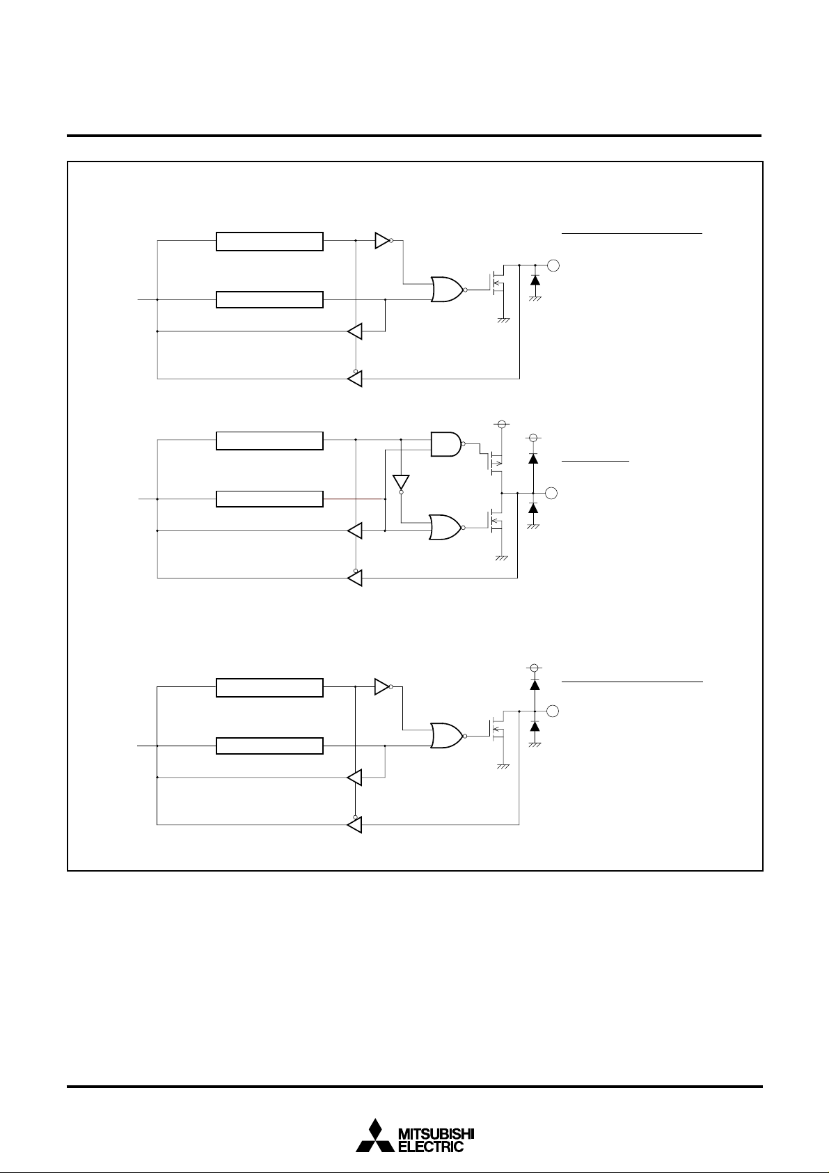
MITSUBISHI MICROCOMPUTERS
M37220M3-XXXSP
SINGLE-CHIP 8-BIT CMOS MICROCOMPUTER for VOLTAGE SYNTHESIZER
with ON-SCREEN DISPLAY CONTROLLER
Ports P0
Ports P06, P07
0–P05, P32
Data bus
Ports P1, P2, P30, P31
Data bus
Direction register
Port latch
Direction register
Port latch
N-channel open drain output
Port P00–P05, P32
Note: Each port is also used as below:
P00–P05 : PWM0–PWM5
CMOS output
Port P1, P2, P30, P31
Note: Each port is also used as below:
P15 : A-D1/INT3
P16 : A-D2
P17 : A-D3
P20 : SCLK
P21 : SOUT
P22 : SIN
P23 : TIM3
P24 : TIM2
P30 : A-D5/DA1
P31 : A-D6/DA2
Data bus
Fig. 44. I/O pin block diagram (1)
Direction register
Port latch
N-channel open-drain output
Port P06, P07
Note: Each port is also used as below:
P06 : INT2/A-D4
P07 : INT1
41

MITSUBISHI MICROCOMPUTERS
M37220M3-XXXSP
SINGLE-CHIP 8-BIT CMOS MICROCOMPUTER for VOLTAGE SYNTHESIZER
with ON-SCREEN DISPLAY CONTROLLER
D-A, R, G, B, OUT HSYNC, VSYNC
Schmidt input
Data bus
Fig. 45. I/O pin block diagram (2)
HSYNC, VSYNC
Data bus
CMOS output
D-A, R, G, B, OUT
Note: Each pin is also used
as below:
R : P52
G : P53
B : P54
OUT : P55
42

SINGLE-CHIP 8-BIT CMOS MICROCOMPUTER for VOLTAGE SYNTHESIZER
XIN
M37220M3-XXXSP
19
Vcc
Vss
External oscillation circuit
CLOCK GENERATING CIRCUIT
The built-in clock generating circuit is shown in Figure 48. When the
STP instruction is executed, the internal clock stops at “H” level.
At the same time, timers 3 and 4 are connected in hardware and
“FF16” is set in the timer 3, “0716” is set in the timer 4. Select f(XIN)/16
as the timer 3 count source (set bit 0 of the timer 34 mode register to
“0” before the execution of the STP instruction). And besides, set the
timer 3 and timer 4 interrupt enable bits to disabled (“0”) before execution of the STP instruction). The oscillator restarts when external
interrupt is accepted, however, the internal clock keeps its “H” level
until timer 4 overflows. Because this allows time for oscillation stabilizing when a ceramic resonator or a quartz-crystal oscillator is used.
When the WIT instruction is executed, the internal clock stops in
the “H” level but the oscillator continues running. This wait state is
released when an interrupt is accepted (Note). Since the oscillator
does not stop, the next instruction can be executed at once.
When returning from the stop or the wait state, to accept an interrupt,
set the corresponding interrupt enable bit to “1” before executing the
STP or the WIT instructions.
MITSUBISHI MICROCOMPUTERS
M37220M3-XXXSP
with ON-SCREEN DISPLAY CONTROLLER
M 37220M 3-XXXSP
XIN XOUT
CIN
Fig. 46. Ceramic resonator circuit example
2019
COUT
Note: In the wait mode, the following interrupts are invalid.
(1) VSYNC interrupt
(2) CRT interrupt
(3) f(XIN)/4096 interrupt
(4) Timer 1 interrupt using f(XIN)/4096 as count source
(5) Timer 2 interrupt using P24/TIM2 pin input as count source
(6) Timer 3 interrupt using P23/TIM3 pin input as count source
(7) Timer 4 interrupt using f(XIN)/2 as count source
(8) Multi-master I2C-BUS interface interrupt
The circuit example using a ceramic resonator (or a quartz-crystal
oscillator) is shown in Figure 46. Use the circuit constants in accordance with the resonator manufacture’s recommended values. The
circuit example with external clock input is shown in Figure 47. Input
the clock to the XIN pin, and open the XOUT pin.
Interrupt request
Interrupt disable
Selection gate :
Connected to black
colored side at reset.
T34M : Timer 34 mode
register
flag I
Reset
STP instruction
Fig. 47. External clock input circuit example
SQ
R
WIT
instruction
SQ
R
SQ
R
STP
instruction
Internal clock
Reset
Fig. 48. Clock generating circuit block diagram
1/2
X
X
IN
OUT
1/8
T34M0
T34M2
Timer 3
Timer 4
43

MITSUBISHI MICROCOMPUTERS
M37220M3-XXXSP
SINGLE-CHIP 8-BIT CMOS MICROCOMPUTER for VOLTAGE SYNTHESIZER
with ON-SCREEN DISPLAY CONTROLLER
DISPLAY OSCILLATION CIRCUIT
The CRT display clock oscillation circuit has a built-in clock oscillation circuits, so that a clock for display can be obtained simply by
connecting an LC, an RC, a ceramic resonator or a quartz-crystal
oscillator circuit across the pins OSC 1 and OSC 2. Select the clock
for display with bits 0 and 1 of the CRT clock selection register (address 00ED
Fig. 49. Display oscillation circuit
16).
C1
OSC2OSC1
L
C2
AUTO-CLEAR CIRCUIT
When power source is supplied, the auto-clear function can be performed by connecting the following circuit to the RESET pin.
Circuit example 1
RESET
______
Vcc
ADDRESSING MODE
The memory access is reinforced with 17 kinds of addressing modes.
Refer to the SERIES 740 <Software> User’s Manual for details.
MACHINE INSTRUCTIONS
There are 71 machine instructions. Refer to the SERIES 740 <Software> User’s Manual for details.
PROGRAMMING NOTES
(1) The divide ratio of the timer is 1/(n+1).
(2) Even though the BBC and BBS instructions are executed imme-
diately after the interrupt request bits are modified (by the program), those instructions are only valid for the contents before
the modification. At least one instruction cycle is needed (such as
an NOP) between the modification of the interrupt request bits
and the execution of the BBC and BBS instructions.
(3) After the ADC and SBC instructions are executed (in decimal
mode), one instruction cycle (such as an NOP) is needed before
the SEC, CLC, or CLD instruction is executed.
(4) An NOP instruction is needed immediately after the execution of
a PLP instruction.
(5) In order to avoid noise and latch-up, connect a bypass capacitor
(≈ 0.1 µF) directly between the V
CNV
SS pin using a thick wire.
CC pin–VSS pin and the VCC pin–
DATA REQUIRED FOR MASK ORDERS
The following are necessary when ordering a mask ROM production:
(1) Mask ROM Order Confirmation Form
(2) Mark Specification Form
(3) Data to be written to ROM, in EPROM form (32-pin DIP type
27C101, three identical copies)
Vss
Circuit example 2
RESET
Note : Make the level change from “L” to “H” at the point at
which the power source voltage exceeds the specified
voltage.
Fig. 50. Auto-clear circuit example
Vcc
Vss
44
ABSOLUTE MAXIMUM RATINGS
Symbol
VCC
VI
VI
VO
VO
IOH
IOL1
IOL2
IOL3
Pd
Topr
Tstg
Power source voltage VCC
Input voltage CNVSS
Input voltage P00–P07,P10–P17, P20–P27,
Output voltage P06, P07, P10–P17, P20–P27,
Output voltage P00–P05
Circuit current R, G, B, OUT, P10–P17,
Circuit current R, G, B, OUT, P06, P07,
Circuit current P00–P05
Circuit current P24–P27
Power dissipation
Operating temperature
Storage temperature
Parameter
P30–P34, OSC1, XIN, HSYNC,
VSYNC, RESET
P30–P32, R, G, B, OUT, D-A,
XOUT, OSC2
P20–P27, P30, P31, D-A
P10–P17, P20–P23, P30–P32,
D-A
MITSUBISHI MICROCOMPUTERS
M37220M3-XXXSP
SINGLE-CHIP 8-BIT CMOS MICROCOMPUTER for VOLTAGE SYNTHESIZER
with ON-SCREEN DISPLAY CONTROLLER
Conditions
All voltages are based
on VSS.
Output transistors are
cut off.
Ta = 25 °C
Ratings
–0.3 to 6
–0.3 to 6
–0.3 to VCC + 0.3
–0.3 to VCC + 0.3
–0.3 to 13
0 to 1 (Note 1)
0 to 2 (Note 2)
0 to 1 (Note 2)
0 to 10 (Note 3)
550
–10 to 70
–40 to 125
Unit
V
V
V
V
V
mA
mA
mA
mA
mW
°C
°C
RECOMMENDED OPERATING CONDITIONS (Ta = –10 °C to 70 °C, VCC = 5 V ± 10 %, unless otherwise noted)
Symbol Parameter Unit
VCC
VSS
VIH1
VIL1
VIL2
IOH
IOL1
IOL2
IOL3
fCPU
fCRT
fhs1
fhs2
Notes 1: The total current that flows out of the IC must be 20 mA (max.).
2: The total input current to IC (IOL1 + IOL2) must be 30 mA or less.
3: The total average input current for ports P24–P27 to IC must be 20 mA or less.
4: Connect 0.1µF or more capacitor externally across the power source pins VCC–VSS so as to reduce power source noise. Also connect
5: Use a quartz-crystal oscillator or a ceramic resonator for the CPU oscillation circuit.
Power source voltage (Note 4), During CPU, CRT operation
Power source voltage
“H” input voltage P00–P07,P10–P17, P20–P27, P30–P34,
SIN, SCLK, HSYNC, VSYNC, RESET, XIN,
OSC1, TIM2, TIM3, INT1, INT2, INT3
“L” input voltage P00–P07,P10–P17, P20–P27, P30–P34
“L” input voltage HSYNC, VSYNC, RESET,TIM2, TIM3, INT1,
INT2, INT3, XIN, OSC1, SIN, SCLK
“H” average output current (Note 1) R, G, B, OUT, D-A, P10–P17, P20–P27,
P30, P31
“L” average output current (Note 2) R, G, B, OUT, D-A, P06, P07,
P10–P17, P20–P27, P30–P32
“L” average output current (Note 2) P00–P05
“L” average output current (Note 3) P24–P27
Oscillation frequency (for CPU operation) (Note 5) XIN
Oscillation frequency (for CRT display) (Note 5) OSC1
Input frequency TIM2, TIM3
Input frequency SCLK
0.1µF or more capacitor externally across the pins VCC–CNVSS.
Min.
4.5
0
0.8VCC
0
0
7.9
5.0
Limits
Typ.
5.0
0
8.0
Max.
5.5
0
VCC
0.4 VCC
0.2 VCC
1
2
1
10
8.1
8.0
100
1
V
V
V
V
V
mA
mA
mA
mA
MHz
MHz
kHz
MHz
45
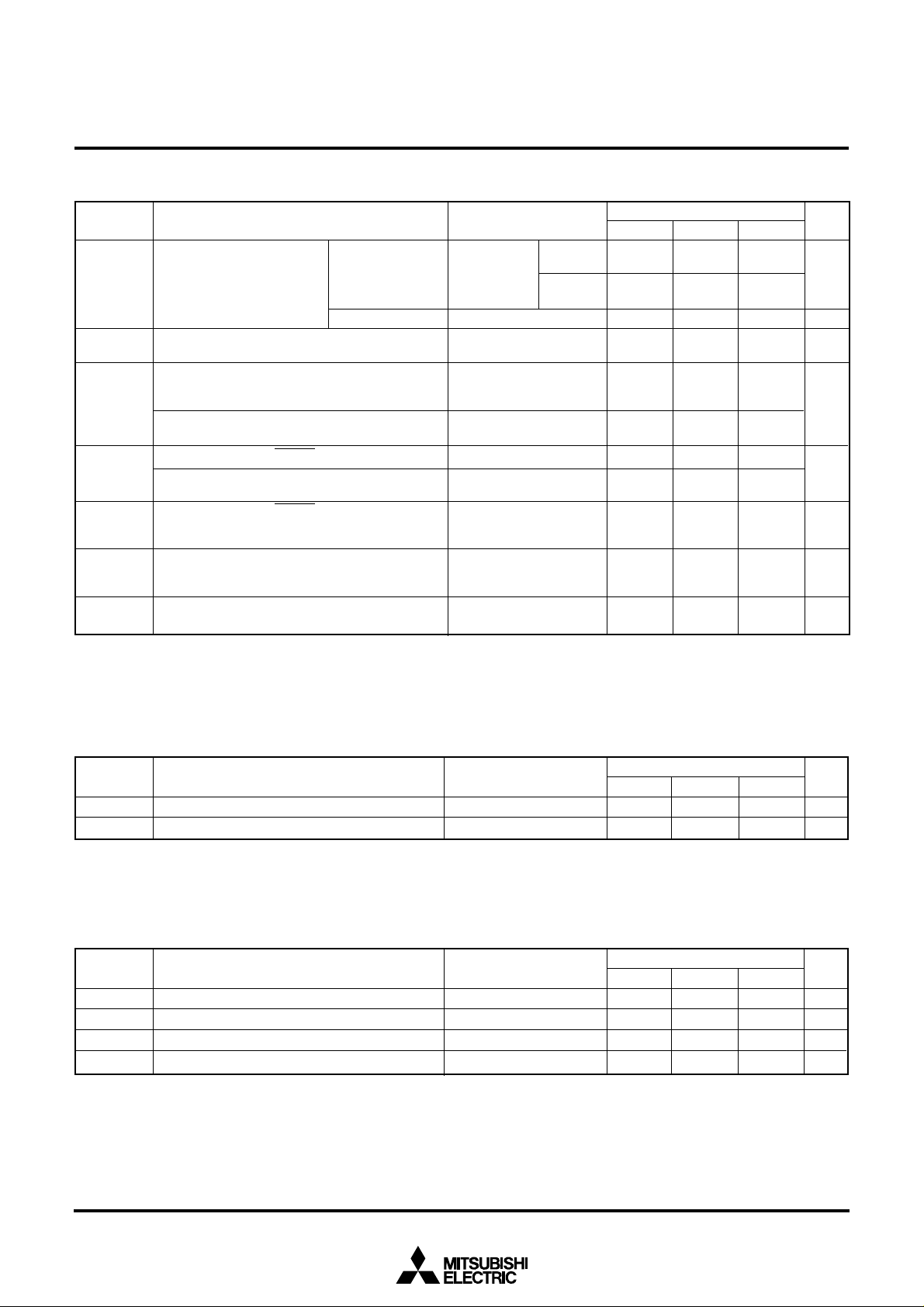
MITSUBISHI MICROCOMPUTERS
M37220M3-XXXSP
SINGLE-CHIP 8-BIT CMOS MICROCOMPUTER for VOLTAGE SYNTHESIZER
with ON-SCREEN DISPLAY CONTROLLER
ELECTRIC CHARACTERISTICS (VCC = 5 V ± 10 %, VSS = 0 V, f(XIN) = 8 MHz, Ta = –10 °C to 70 °C, unless otherwise noted)
Symbol
ICC
Power source current
Parameter Test conditions Unit
System operation
VCC = 5.5 V,
f(XIN) = 8 MHz
CRT OFF
CRT ON
Min.
Limits
Typ.
20
30
Max.
40
60
mA
Stop mode
VOH
VOL
VT+–VT–
IIZH
IIZL
IOZH
Note:P06, P07, P15, P23, P24 have the hysteresis when these pins are used as interrupt input pins or timer input pins. P20–P22 have the
hysteresis when these pins are used as serial I/O pins.
“H” output voltage R, G, B, OUT, D-A, P10–P17,
“L” output voltage R, G, B, OUT, D-A, P00–P07,
“L” output voltage P24–P27
Hysteresis RESET
Hysteresis (Note) HSYNC, VSYNC, TIM2, TIM3,
“H” input leak currentRESET, P00–P07, P10–P17,
“L” input leak current
“H” output leak current P00–P05
P20–P27, P30, P31
P10–P17, P20–P23,
P30–P32
INT1, INT2, INT3, SIN, SCLK
P20–P27, P30–P34, HSYNC,
VSYNC
______
RESET, P00–P07, P10–P17,
P20–P27, P30–P34, HSYNC,
VSYNC
VCC = 5.5 V, f(XIN) = 0
VCC = 4.5 V
IOH = –0.5 mA
VCC = 4.5 V
IOL = 0.5 mA
VCC = 4.5 V
IOL = 10.0 mA
VCC = 5.0 V
VCC = 5.0 V
VCC = 5.5 V
VI = 5.5 V
VCC = 5.5 V
VO = 0 V
VCC = 5.5 V
VI = 12 V
2.4
0.5
0.5
300
0.4
3.0
0.7
1.3
5
5
10
µA
V
V
V
µA
µA
µA
A-D COMPARATOR CHARACTERISTICS
(VCC = 5 V ± 10 %, VSS = 0 V, f(XIN) = 8 MHz, Ta = –10 °C to 70 °C, unless otherwise noted)
Symbol
—
—
Note: When V
Parameter
Resolution
Absolute accuracy
CC = 5 V, 1 LSB = 5/64 V.
Min.
0
Limits
Typ.
±1
Max.
6
±2
UnitTest conditions
bits
LSB
D-A CONVERTER CHARACTERISTICS
(VCC = 5 V ± 10 %, VSS = 0 V, f(XIN) = 8 MHz, Ta = –10 °C to 70 °C, unless otherwise noted)
46
Symbol
—
—
tsu
R
O
Resolution
Absolute accuracy
Setting time
Output resistor
Parameter
Min.
1
Limits
Typ.
2.5
Max.
6
2
3
4
UnitTest conditions
bits
%
µs
kΩ

PACKAGE OUTLINE
MITSUBISHI MICROCOMPUTERS
M37220M3-XXXSP
SINGLE-CHIP 8-BIT CMOS MICROCOMPUTER for VOLTAGE SYNTHESIZER
with ON-SCREEN DISPLAY CONTROLLER
47

GZZ–SH09–72B < 56A0 >
MITSUBISHI MICROCOMPUTERS
M37220M3-XXXSP
SINGLE-CHIP 8-BIT CMOS MICROCOMPUTER for VOLTAGE SYNTHESIZER
with ON-SCREEN DISPLAY CONTROLLER
740 FAMILY MASK ROM CONFIRMATION FORM
SINGLE-CHIP MICROCOMPUTER M37220M3-XXXSP
MITSUBISHI ELECTRIC
Company
❈
Customer
name
Date
issued
Date :
TEL
( )
Mask ROM number
Date :
Section head
signature
Receipt
Note : Please fill in all items marked ❈.
Submitted by
Issuance
signature
❈ 1. Confirmation
Specify the name of the product being ordered and the type of EPROMs submitted.
Three EPROMs are required for each pattern.
If at least two of the three sets of EPROMs submitted contain identical data, we will produce masks based on
this data. We shall assume the responsibility for errors only if the mask ROM data on the products we produce
differs from this data. Thus, extreme care must be taken to verify the data in the submitted EPROMs.
Checksum code for entire EPROM
(hexadecimal notation)
EPROM type (indicate the type used)
27C101
EPROM address
0000
000F
D000
FFFF
10000
107FF
10800
10FFF
11000
1FFFF
16
Product name
ASCII code :
‘M37220M3 –’
16
16
ROM 12K bytes
16
16
Character ROM 1
16
16
Character ROM 2
16
16
16
data
Supervisor
signature
Supervisor
48
(1)
Set “FF16” in the shaded area.
(2)
Write the ASCII codes that indicates the product name of “M37220M3–” to addresses 0000
16
to 000F16.
EPROM data check item (Refer the EPROM data and check “✓” in the appropriate box)
Do you set “FF
●
●
Do you write the ASCII codes that indicates the product
name of “M37220M3–” to addresses 0000
16
” in the shaded area ?
16
to 000F
→ Yes ■
→ Yes ■
16
?
❈ 2. Mark specification
Mark specification must be submitted using the correct form for the type package being ordered fill out the appropriate
mark specification form (42P4B for M37220M3-XXXSP) and attach to the mask ROM confirmation form.
❈ 3. Comments
(1/3)

MITSUBISHI MICROCOMPUTERS
M37220M3-XXXSP
SINGLE-CHIP 8-BIT CMOS MICROCOMPUTER for VOLTAGE SYNTHESIZER
with ON-SCREEN DISPLAY CONTROLLER
GZZ–SH09–72B <56A0 >
740 FAMILY MASK ROM CONFIRMATION FORM
SINGLE-CHIP MICROCOMPUTER M37220M3-XXXSP
MITSUBISHI ELECTRIC
Writing the product name and character ROM data onto EPROMs
16
Addresses 0000
If the name of the product contained in the EPROMs does not match the name on the mask ROM confirmation form,
the ROM processing is disabled. Write the data correctly.
to 000F16 store the product name, and addresses 1000016 to 10FFF16 store the character pattern.
1.
Inputting the name of the product with the ASCII code
ASCII codes ‘M37220M3-’ are listed on the right.
The addresses and data are in hexadecimal notation.
2.
Inputting the character ROM
Address
0000
0001
0002
0003
0004
0005
0006
0007
16
16
16
16
16
16
16
16
=
‘M’
4D
=
‘3’
33
37
‘7’
=
‘2’=32
‘2’=32
30
=
‘0’
‘M’=4D
‘3’=33
Address
=
‘–’
16
0008
16
0009
000A
000B
000C
000D
000E
000F
16
16
16
16
16
16
16
16
16
16
16
16
16
16
2
FF
FF
FF
FF
FF
FF
FF
Input the character ROM data by dividing it into character ROM1 and character ROM2. For the character ROM data,
see the next page and on.
D
16
16
16
16
16
16
16
16
(2/3)
49

SINGLE-CHIP 8-BIT CMOS MICROCOMPUTER for VOLTAGE SYNTHESIZER
GZZ–SH09–72B< 56A0 >
740 FAMILY MASK ROM CONFIRMATION FORM
SINGLE-CHIP MICROCOMPUTER M37220M3-XXXSP
MITSUBISHI ELECTRIC
The structure of character ROM (divided of 12✕16 dots font)
Example
Character code
“1A
16”
MITSUBISHI MICROCOMPUTERS
M37220M3-XXXSP
with ON-SCREEN DISPLAY CONTROLLER
Example
101A0
to
101AF
b7
b6 b5 b4 b3 b2 b1 b0
16
0
1
16
2
3
4
5
6
7
8
9
A
B
C
D
E
F
⇐
Character
ROM1
0
16
0
416
0
0416
A16
0
A16
0
116
1
116
1
116
1
016
2
016
2
F16
3
016
4
016
4
016
4
016
0
016
0
Character
ROM2
Example
109A0
to
109AF
⇐
16
16
b7
b6 b5 b4 b3 b2 b1 b0
0
1
2
3
4
5
6
7
F16
8
9
A
B
C
D
E
F
F0
F016
F016
F016
F016
F016
F016
F016
F816
F816
F816
F416
F416
F416
F016
F016
16
50
(3/3)

MITSUBISHI MICROCOMPUTERS
M37220M3-XXXSP
SINGLE-CHIP 8-BIT CMOS MICROCOMPUTER for VOLTAGE SYNTHESIZER
with ON-SCREEN DISPLAY CONTROLLER
51

MITSUBISHI DATA BOOK
SINGLE-CHIP 8-BIT MICROCOMPUTERS Vol.3
Sep. First Edition 1996 H-DF319-B
Editioned by
Committee of editing of Mitsubishi Semiconductor Data Book
Published by
Mitsubishi Electric Corp., Semiconductor Division
This book, or parts thereof, may not be reproduced in any form without permission of
Mitsubishi Electric Corporation.
©1996 MITSUBISHI ELECTRIC CORPORATION Printed in Japan

REVISION DESCRIPTION LIST
M37220M3-XXXSP DATA SHEET
Rev. Rev.
No. date
1.0 First Edition 9708
2.0 Information about copywright note, revision number, release data added (last page). 971130
2.1 Correct note (P43) 980731
Revision Description
(1/1)
 Loading...