

Mitsubishi M37212M8-XXXSP, M37212M6-XXXSP, M37212M6-XXXFP, M37212EFSP, M37212EFFP Datasheet

To all our customers
Regarding the change of names mentioned in the document, such as Mitsubishi
Electric and Mitsubishi XX, to Renesas Technology Corp.
The semiconductor operations of Hitachi and Mitsubishi Electric were transferred to Renesas
Technology Corporation on April 1st 2003. These operations include microcomputer, logic, analog
and discrete devices, and memory chips other than DRAMs (flash memory, SRAMs etc.)
Accordingly, although Mitsubishi Electric, Mitsubishi Electric Corporation, Mitsubishi
Semiconductors, and other Mitsubishi brand names are mentioned in the document, these names
have in fact all been changed to Renesas Technology Corp. Thank you for your understanding.
Except for our corporate trademark, logo and corporate statement, no changes whatsoever have been
made to the contents of the document, and these changes do not constitute any alteration to the
contents of the document itself.
Note : Mitsubishi Electric will continue the business operations of high frequency & optical devices
and power devices.
Renesas Technology Corp.
Customer Support Dept.
April 1, 2003

MITSUBISHI MICROCOMPUTERS
M37212M4/M8–XXXSP, M37212M6–XXXSP/FP
M37212EFSP/FP
SINGLE-CHIP 8-BIT CMOS MICROCOMPUTER for VOLTAGE SYNTHESIZER
with ON-SCREEN DISPLAY CONTROLLER
1. DESCRIPTION
The M37212M6-XXXSP/FP, M37212M4/M8-XXXSP are single-chip
microcomputers designed with CMOS silicon gate technology. They
have a OSD, I2C-BUS interface, and PWM, so it is useful for a channel selection system for TV.
The feature of the M37212EFSP/FP are similar to those of the
M37212M6-XXXSP/FP except that these chips have a built-in PROM
which can be written electrically. The differences between the
M37212M6-XXXSP/FP and M37212M4/M8-XXXSP are the ROM size
and the RAM size as shown below. Accordingly, the following descriptions will be for M37212M6-XXXSP/FP unless otherwise noted.
2. FEATURES
●Number of basic instructions ..................................................... 71
●Memory size
ROM............... .........16K bytes (M37212M4-XXXSP)
24K bytes (M37212M6-XXXSP/FP)
32K bytes (M37212M8-XXXSP)
62K bytes (M37212EFSP/FP)
RAM .........................320 bytes (M37212M4-XXXSP)
384 bytes (M37212M6-XXXSP/FP)
576 bytes (M37212M8-XXXSP)
1280 bytes (M37212EFSP/FP)
(*ROM correction memory included)
●The minimum instruction execution time
.........................................0.5 µs (at 8 MHz oscillation frequency)
●Power source voltage .................................................. 5 V ± 10 %
●Subroutine nesting
maximum 96 levels (M37212M4/M8-XXXSP, M37212M6-XXXSP/FP)
maximum 128 levels (M37212EFSP/FP)
●Interrupts........................................................ 14 types, 14 vectors
●8-bit timers ................................................................................... 4
●Programmable I/O ports
(Ports P0, P10–P14, P2, P30, P31, P40, P41) ............................. 25
●Input ports (Ports P15–P17, P32–P37, P42) ............................... 10
●Output ports (Ports P52–P55, P60–P63)....................................... 8
●12 V withstand ports .................................................................. 12
●LED drive ports ............................................................................ 4
●Serial I/O............................................................. 8-bit ✕ 1 channel
●Multi-master I
●A-D comparator (6-bit resolution) .................................8 channels
●PWM output circuit..........................................14-bit ✕ 1, 8-bit ✕ 8
●Power dissipation..............................................................165 mW
●ROM correction function ................................................. 2 vectors
Note: Only M37212M8-XXXSP and M37212EFSP/FP have ROM
2
C-BUS interface ............................... 1 (2 systems)
(at 8 MHz oscillation frequency, VCC=5.5V, at OSD display)
correction function.
●OSD function
Display characters ................................... 24 characters ✕ 2 lines
(It is possible to display 3lines or more by software)
Kinds of characters ........................................................256 kinds
Character display area..............................................12 ✕ 16 dots
Kinds of character sizes..................................................... 3 kinds
Kinds of character colors .................................. 8 colors (R, G, B)
Coloring unit................... character, character background, raster
Display position.............................................................................
Horizontal: 64 levels Vertical: 128 levels
Attribute ..............................................................................border
3. APPLICA TION
TV
Rev. 1.0

M37212M4/M8–XXXSP, M37212M6–XXXSP/FP
SINGLE-CHIP 8-BIT CMOS MICROCOMPUTER for VOLTAGE SYNTHESIZER
TABLE OF CONTENTS
1. DESCRIPTION ..........................................................................1
2. FEAUTURES .............................................................................1
3. APPLICATION............................................................................1
4. PIN CONFIGURATION ..............................................................3
5. FUNCTIONAL BLOCK DIAGRAM .............................................5
6. PERFORMANCE OVERVIEW...................................................6
7. PIN DESCRIPTION ...................................................................8
8. FUNCTIONAL DESCRIPTION.................................................12
8.1 CENTRAL PROCESSING UNIT (CPU) .................... 12
8.2 MEMORY ..................................................................13
8.3 INTERRUPTS ...........................................................19
8.4 TIMERS.....................................................................24
8.5 SERIAL I/O................................................................27
8.6 MULTI-MASTER I2C-BUS INTERFACE....................31
8.7 PWM OUTPUT CIRCUIT ..........................................44
8.8 A-D COMPARA TOR ..................................................49
8.9 ROM CORRECTION FUNCTION .............................51
8.10 OSD FUNCTIONS...................................................52
8.10.1 Display Position .......................................56
8.10.2 Character Size.........................................60
8.10.3 Clock for OSD..........................................62
8.10.4 Memory for OSD......................................63
8.10.5 Color Register..........................................66
8.10.6 Border......................................................68
8.10.7 Multiline Display.......................................69
8.10.8 OSD Output Pin Control ..........................70
8.10.9 Raster Coloring Function.........................71
8.11. SOFTWARE RUNAWAY DETECT FUNCTION......72
8.12. RESET CIRCUIT....................................................73
8.13. CLOCK GENERATING CIRCUIT...........................74
8.14. DISPLAY OSCILLATION CIRCUIT ........................75
8.15. AUTO-CLEAR CIRCUIT .........................................75
8.16. ADDRESSING MODE ............................................75
8.17. MACHINE INSTRUCTIONS...................................75
9. PROGRAMMING NOTES........................................................75
10. ABSOLUTE MAXIMUM RATINGS .........................................76
11. RECOMMENDED OPERATING CONDITIONS.....................76
12. ELECTRIC CHARACTERISTICS ..........................................77
13. A-D COMPARISON CHARACTERISTICS.............................79
14.
MULTI-MASTER I2C-BUS BUS LINE CHARACTERISTICS ...........
15. PROM PROGRAMMING METHOD.......................................80
16. DATA REQUIRED FOR MASK ORDERS..............................81
17. MASK CONFIRMATION FORM.............................................82
18. MARK SPECIFICATION FORM.............................................91
19.
ONE TIME PROM VERSIONS M37212EFSP/FP MARKING ....
20. APPENDIX .............................................................................94
21. PACKAGE OUTLINE ........................................................... 117
79
93
MITSUBISHI MICROCOMPUTERS
M37212EFSP/FP
with ON-SCREEN DISPLAY CONTROLLER
Rev. 1.0
2
0
2
3
4
5
6
7
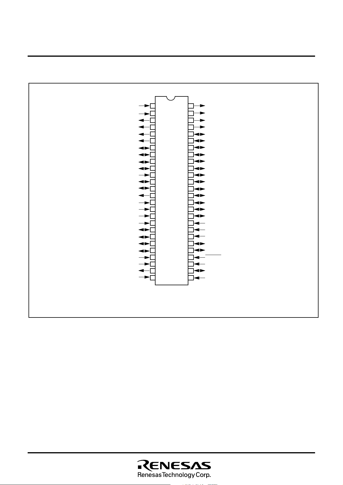
4. PIN CONFIGURATION
MITSUBISHI MICROCOMPUTERS
M37212M4/M8–XXXSP, M37212M6–XXXSP/FP
M37212EFSP/FP
SINGLE-CHIP 8-BIT CMOS MICROCOMPUTER for VOLTAGE SYNTHESIZER
with ON-SCREEN DISPLAY CONTROLLER
3 7 2 1 2 M 4 / M 6 / M 8 - X X X S P , M 3 7 2 1 2 E F S
H
P 60/ P W M
P 61/ P W M 1
P 6
P 63/ P W M
P 00/ P W M
P 01/ P W M
P 02/ P W M
P 03/ P W M
P 42/ S
P 41/ S
C L K
P 40/ S
O U T ( / I N )
P 35/ I N T 2 / A - D 4
P 3
P 33/ T I M 3
P 3
V
2
/ P W M
I N
/ A - D 5
/ A - D 6
/ A - D 7
4
/ I N T 1
2
/ T I M 2
C N V
X
S Y N C
S Y N C
D A
P 2
P 2
P 2
P 2
X
O U T
V
1
2
3
4
5
6
7
8
9
1 0
1 1
1 2
1 3
1 4
1 5
1 6
1 7
1 8
4
1 9
5
2 0
6
2 1
7
2 2
S S
2 3
I N
2 4
2 5
2 6
S S
M
P
5 2
5 1
5 0
4 9
4 8
4 7
4 6
4 5
4 4
4 3
4 2
4 1
4 0
3 9
3 8
3 7
3 6
3 5
3 4
3 3
3 2
3 1
3 0
2 9
2 8
2 7
P 52/ R
P 53/ G
P 54/ B
P 55/ O U T 1
0
P 2
P 2
1
P 2
2
P 2
3
P 0
4
P 0
5
P 0
6
P 0
7
P 10/ O U T 2 / A - D 8
1
/ S C L 1
P 1
P 12/ S C L 2
P 13/ S D A 1
4
/ S D A 2
P 1
P 15/ I N T 3 / A - D 1
P 16/ A - D 2
P 17/ A - D 3
0
P 3
P 31
R E S E T
O S C 1 / P 3
O S C 2 / P 3
V
6
7
C C
Fig. 4.1 Pin Configuration 1 (Top View)
Rev. 1.0
Outline 52P4B
3
MITSUBISHI MICROCOMPUTERS
M37212M4/M8–XXXSP, M37212M6–XXXSP/FP
M37212EFSP/FP
SINGLE-CHIP 8-BIT CMOS MICROCOMPUTER for VOLTAGE SYNTHESIZER
with ON-SCREEN DISPLAY CONTROLLER
8
/
5
1
I N T 3 / A - D 1P
A - D 2
P
/
/
6
7
C
1
C
1
A - D 3
P
N
N
CN
CN
2
2
/
S C L
/
2
1
S D A 1P
/
3
4
C
1
1
P
S D A
N
/
2
3
C
N
CN
CN
CN
4
2
2
0
P
P
P
75
5
6
0
0
0
P
P
P
/
0
1
C
1
1
O U T 2 / A - D
P
S C L 1P
P
N
P 2
N C
P 2
5
/ O U T 1
P 5
P 5
4
/ B
3
/ G
P 5
P 52/ R
N C
N C
H
S Y N C
V
S Y N C
P 60/ P W M 0
P 6
1
/ P W M 1
P 6
2
/ P W M 2
N C
P 6
3
/ P W M 3
3
1
8
9
7
4
6
6
6
1
0
6 5
6 6
6 7
6 8
6 9
7 0
7 1
7 2
7 3
7 4
7 5
7 6
7 7
7 8
7 9
8 0
1234567
C
N
C
C
N
N
5
6
6
M 3 7 2 1 2 M 6 - X X X F P , M 3 7 2 1 2 E F F P
5
4
C
N
/
/
1
0
0
0
P
P
P W M
P W M
0
1
3
2
6
4
5
6
/
2
0
P
P W M
5
5
5
5
5
0
1
8
9
7
C
N
/
3
0
P
P W M
2
1
1
1
7
5
6
/
/
/
)
K
N
I
S
C
/
2
S
/
4
1
O
P
4
S
/
P
0
4
A - D
A - D
L
P
A - D
U T ( / I N
0
2
5
3
1
A
D
9
5
5
4
4
5
6
1
1
1
1
4
3
/
/
4
3
3
3
P
P
/
5
I N T
3
T I M
P
I N T 2 / A - D
6
7
8
4
4
4
7
8
9
1
1
1
5
4
2
2
2
P
P
/
2
3
P
T I M
3
4
5
4
4
0
1
2
2
6
C
2
N
P
1
2
4
4
4
2
2
C
N
4 0
3 9
3 8
3 7
3 6
3 5
3 4
3 3
3 2
3 1
3 0
2 9
2 8
2 7
2 6
2 5
4
3
2
2
C
C
N
N
P 3
0
N C
P 31
R E S E T
O S C 1 / P 3
O S C 2 / P 3
V
C C
N C
N C
V
S S
X
O U T
X
I N
C N V
S S
P
2
7
N C
N C
6
7
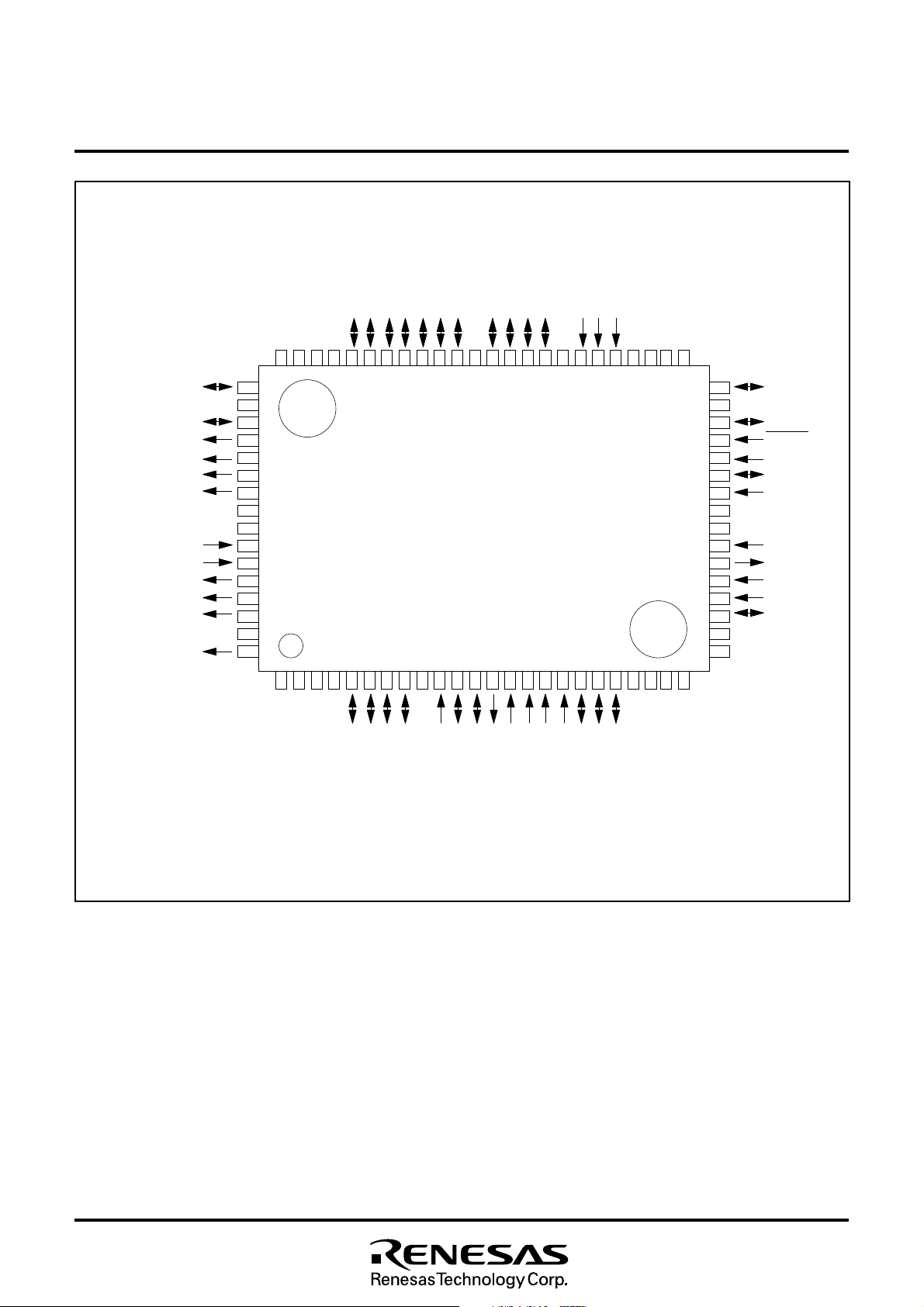
Fig. 4.2 Pin Configuration 2 (Top View)
4
Outline 80P6N-A
NC : Unconnected
Rev. 1.0
M37212M4/M8–XXXSP, M37212M6–XXXSP/FP
OUT1
Clock input Clock output
X
IN
X
OUT
Reset input
V
CC
V
SS
CNV
SS
Clock output for display
Input ports P3
6,
P3
7
OSC1 OSC2
Clock input for display
INT2
INT1
P5 (4)
B
G
R
H
SYNC
V
SYNC
A-D
comparator
14-bit
PWM circuit
8-bit PWM circuit
Accumulator
A (8)
Timer 4
T4 (8)
Timer 3
T3 (8)
Timer 2
T2 (8)
Timer 1
T1 (8)
Timer count source
selection circuit
TIM2
TIM3
Instruction
register (8)
Instruction
decoder
Control signal
CRT circuit
Stack
pointer
S (8)
Index
register
Y (8)
Index
register
X (8)
Processor
status
register
PS (8)
8-bit
arithmetic
and
logical unit
ROM
Program
counter
PC
L
(8)
Program
counter
PC
H
(8)
RAM
Data bus
Clock
generating
circuit
RESET
Output ports P5
2
–P5
5
Address bus
SI/O(8)
S
IN
S
CLK
S
OUT(/IN)
INT3
4142 434410 9 8 7
I/O port P0
3334353637383940
P1 (8)
I/O ports P1
0
–P1
4
2221 201945 464748
P2 (8)
I/O port P2
I/O ports P3
0
, P3
1
18 313214
P3 (6)
Multi-master
I C-BUS interface
P0 (8)
SDA
SCL
49 5051
52 2 1
2524
30
27 26
23
29
28
( ) Timing output
OUT2
DA
2
1516 17
P4 (3)
111213
PWM5
PWM4
PWM3
PWM2
PWM1
PWM0
PWM7
PWM6
Input ports P1
5
–P1
7
Input ports P3
2
–P3
5
P6 (4)
Output ports P6
0
–P6
3
6
5 4 3
I/O ports P4
0
, P4
1
Input port P4
2
Output for display
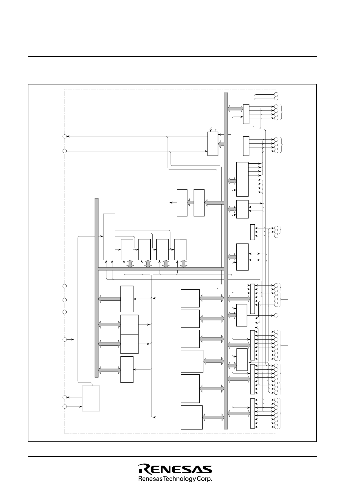
5. FUNCTIONAL BLOCK DIAGRAM
MITSUBISHI MICROCOMPUTERS
M37212EFSP/FP
SINGLE-CHIP 8-BIT CMOS MICROCOMPUTER for VOLTAGE SYNTHESIZER
with ON-SCREEN DISPLAY CONTROLLER
Fig. 5.1 Functional Block Diagram of M37212
Rev. 1.0
5
MITSUBISHI MICROCOMPUTERS
M37212M4/M8–XXXSP, M37212M6–XXXSP/FP
M37212EFSP/FP
SINGLE-CHIP 8-BIT CMOS MICROCOMPUTER for VOLTAGE SYNTHESIZER
with ON-SCREEN DISPLAY CONTROLLER
6. PERFORMANCE OVERVIEW
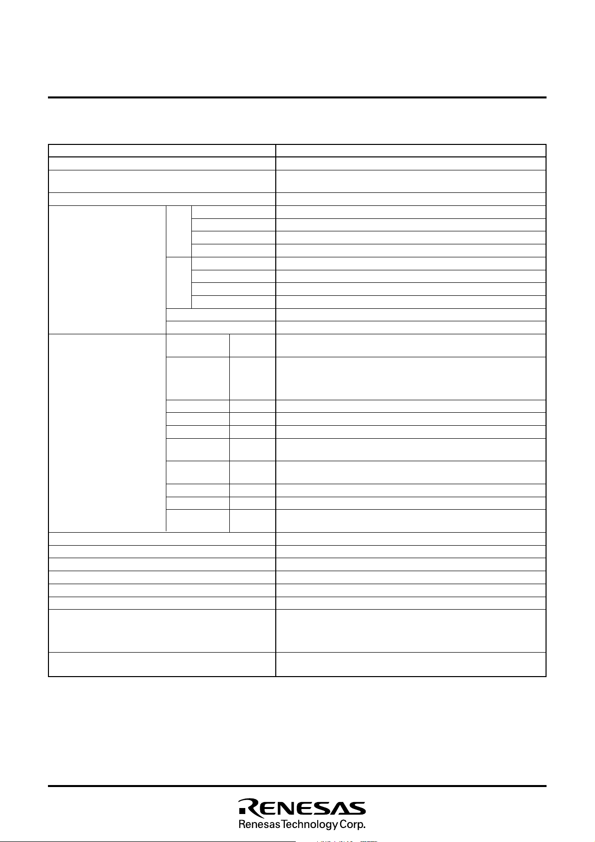
Table 6.1 Performance Overview
Parameter Functions
Number of basic instructions 71
Number of basic instructions 0.5 µs (the minimum instruction execution time, at 8 MHz oscillation fre
Instruction execution time 8 MHz (maximum)
Memory size ROM M37212M4-XXXSP 16K bytes
M37212M6-XXXSP/FP
M37212M8-XXXSP 32K bytes
M37212EFSP/FP 62K bytes
RAM M37212M4-XXXSP 320 bytes
M37212M6-XXXSP/FP
M37212M8-XXXSP 576 bytes (ROM correction memory included)
M37212EFSP/FP 1280 bytes (ROM correction memory included)
OSD ROM 8 K bytes
OSD RAM 96 bytes
Input/Output ports P0 I/O 8-bit ✕ 1 (N-channel open-drain output structure, can be used as PWM
P10–P14 I/O 5-bit ✕ 1 (CMOS input/output output structure, however, N-channel open-
P15–P17 Input 3-bit ✕ 1 (can be used as INT input pin, A-D input pins)
P20–P27 I/O 8-bit ✕ 1 (CMOS input/output structure)
P30, P31 I/O 2-bit ✕ 1 (CMOS input/output structure)
P32–P37 Input 6-bit ✕ 1 (can be used as external clock input pins, INT input pins, OSD
P40, P41 I/O 2-bit ✕ 1 (N-channel open-drain output structure, can be used as serial I/O
P42 Input 1-bit ✕ 1(can be used as serial input pin, A-D input pin)
P52–P55 Output 4-bit ✕ 1 (CMOS output structure, can be used as OSD output pins)
P60–P63 Output 4-bit ✕ 1 (N-channel open-drain output structure, can be used as PWM
Serial I/O 8-bit ✕ 1
Multi-master I2C-BUS interface 1 (2 systems)
A-D comparator 8 channels (6-bit resolution)
PWM output circuit 14-bit ✕ 1, 8-bit ✕ 8
Timers 8-bit timer ✕ 4
Subroutine nesting 96 levels (maximum)
Interrupt <14 sources>
Clock generating circuit 2 built-in circuits (externally connected a ceramic resonator or a quartz-
quency)
24K bytes
384 bytes
output pins)
drain output structure, when P11–P14 are used as multi-master I2C-BUS
interface, can be used as OSD output, A-D input, multi-master I2C-BUS
interface)
display clock I/O pins, A-D input pins)
pins, A-D input pins)
output pins)
INT external interrupt ✕ 3, Internal timer interrupt ✕ 4, Serial I/O interrupt ✕
OSD interrupt ✕ 1, Multi-master I2C-BUS interface interrupt ✕ 1, f(XIN)/
interrupt ✕ 1, VSYNC interrupt ✕ 1, BRK interrupt ✕ 1, Reset ✕ 1
crystal oscillator)
1,
4096
Rev. 1.0
6
MITSUBISHI MICROCOMPUTERS
M37212M4/M8–XXXSP, M37212M6–XXXSP/FP
M37212EFSP/FP
SINGLE-CHIP 8-BIT CMOS MICROCOMPUTER for VOLTAGE SYNTHESIZER
with ON-SCREEN DISPLAY CONTROLLER
Table 6.2 Performance Overview (continued)
Parameter Functions
OSD display Number of display characters 24 characters ✕ 2 lines
function
Power source voltage 5 V ± 10 %
Power dissipation OSD ON 165 mW typ. (at oscillation frequency f(XIN) = 8 MHz, fOSC = 8 MHz)
Operating temperature range –10 °C to 70 °C
Device structure CMOS silicon gate process
Package M37212M4/M6/M8-XXXSP, M37212EFSP 52-pin plastic molded SDIP
Dot structure 12 ✕ 16 dots
Kinds of characters 254 kinds
Kinds of character sizes 3 kinds
Character font coloring 1 screen: 8 kinds (per character unit)
Display position Horizontal: 64 levels, Vertical: 128 levels
OSD OFF 110 mW typ. (at oscillation frequency f(XIN) = 8 MHz)
In stop mode 1.65 mW (maximum)
M37212M6-XXXFP, M37212EFSP 80-pin plastic molded QFP
Rev. 1.0
7
MITSUBISHI MICROCOMPUTERS
M37212M4/M8–XXXSP, M37212M6–XXXSP/FP
M37212EFSP/FP
SINGLE-CHIP 8-BIT CMOS MICROCOMPUTER for VOLTAGE SYNTHESIZER
with ON-SCREEN DISPLAY CONTROLLER
7. PIN DESCRIPTION
Table 7.1 Pin Description
Pin Name
VCC, Power source Apply voltage of 5 V ± 10 % to (typical) VCC, and 0 V to VSS.
VSS.
CNVSS CNVSS This is connected to VSS.
______
RESET Reset input Input To enter the reset state, the reset input pin must be kept at a “L” for 2 µs or more (under
XIN Clock input Input This chip has an internal clock generating circuit. To control generating frequency, an
XOUT Clock output Output XOUT. If an external clock is used, the clock source should be connected to the XIN pin and
P00/PWM4–
P03/PWM7,
P04–P07 is N-channel open-drain output. (See note)
P10/OUT2/
A-D8,
P11/SCL1,
P12/SCL2,
P13/SDA1, I2C-BUS interface I2C-BUS interface is used. The output structure is N-channel open-drain output.
P14/SDA2, Analog input Input P10 pin is also used as analog input pin A-D8.
P15/INT3/ Input port P1 Input Port P15–P17 are a 3-bit input port and has basically the same functions as port P0.
A-D1,
P16/A-D2,
P17/A-D3 input
P20–P27 I/O port P2 I/O Port P2 is an 8-bit I/O port and has basically the same functions as port P0. The output
P30, P31 I/O port P3 I/O Ports P30, P31 are a 2-bit I/O port and has basically the same functions as port P0. The
P32/TIM2, Input port P3 Input Ports P32–P37 are a 6-bit input port and has basically the same functions as port P0.
P33/TIM3,
P34/INT1, External interrupt Input Pins P34, P35 are also used as INT external interrupt input pins INT1, INT2 respectively.
P35/INT2/
A-D4, Analog input Input P35 pin is also used as analog input pin A-D4.
P36/OSC1,
P37/OSC2
I/O port P0 I/O Port P0 is an 8-bit I/O port with direction register allowing each I/O bit to be individually
PWM output Output Pins P00–P03 are also used as PWM output pins PWM4–PWM7 respectively. The output
I/O port P1 I/O Port P10–P14 are a 5-bit I/O port and has basically the same functions as port P0. The
OSD output Output Pins P10 is also used as OSD output pin OUT2. The output structure is CMOS output.
Multi-master I/O Pins P11–P14 are used as SCL1, SCL2, SDA1 and SDA2 respectively, when multi-master
Analog input Input Pins P15–P17 are also used as analog input pins A-D1 to A-D3 respectively.
External interrupt Input P15 pin is also used as INT external interrupt input pin INT3.
External clock input
input
Clock input for Input P36 pin is also used as OSD display clock input pin OSC1.
OSD display
Clock output for Output P37 pin is also used as OSD display clock output pin OSC2. The output structure is CMOS
OSD display output.
Input/
Output
normal VCC conditions).
If more time is needed for the quartz-crystal oscillator to stabilize, this “L” condition should
be maintained for the required time.
external ceramic resonator or a quartz-crystal oscillator is connected between pins XIN and
the XOUT pin should be left open.
programmed as input or output. At reset, this port is set to input mode. The output structure
structure is N-channel open-drain output.
output structure is CMOS output.
structure is CMOS output. (See note)
output structure is CMOS output.
Input Pins P32, P33 are also used as external clock input pins TIM2, TIM3 respectively.
Functions
Rev. 1.0
8
MITSUBISHI MICROCOMPUTERS
M37212M4/M8–XXXSP, M37212M6–XXXSP/FP
M37212EFSP/FP
SINGLE-CHIP 8-BIT CMOS MICROCOMPUTER for VOLTAGE SYNTHESIZER
with ON-SCREEN DISPLAY CONTROLLER
Table 7.2 Pin Description (continued)
Pin Name
P40/SOUT(/IN)/
A-D7, output structure is N-channel open-drain output.
P41/SCLK/ Serial I/O data I/O Pin P40 is also used as serial I/O data input/output pin SOUT(/IN). The output structure is NA-D6, input/output channel open-drain output.
P42/SIN/ Input port P4 Input Port P42 is a 1-bit input port and has basically the same functions as port P0.
A-D5, Serial I/O data Input Pin P42 is also used as serial I/O data input pin SIN.
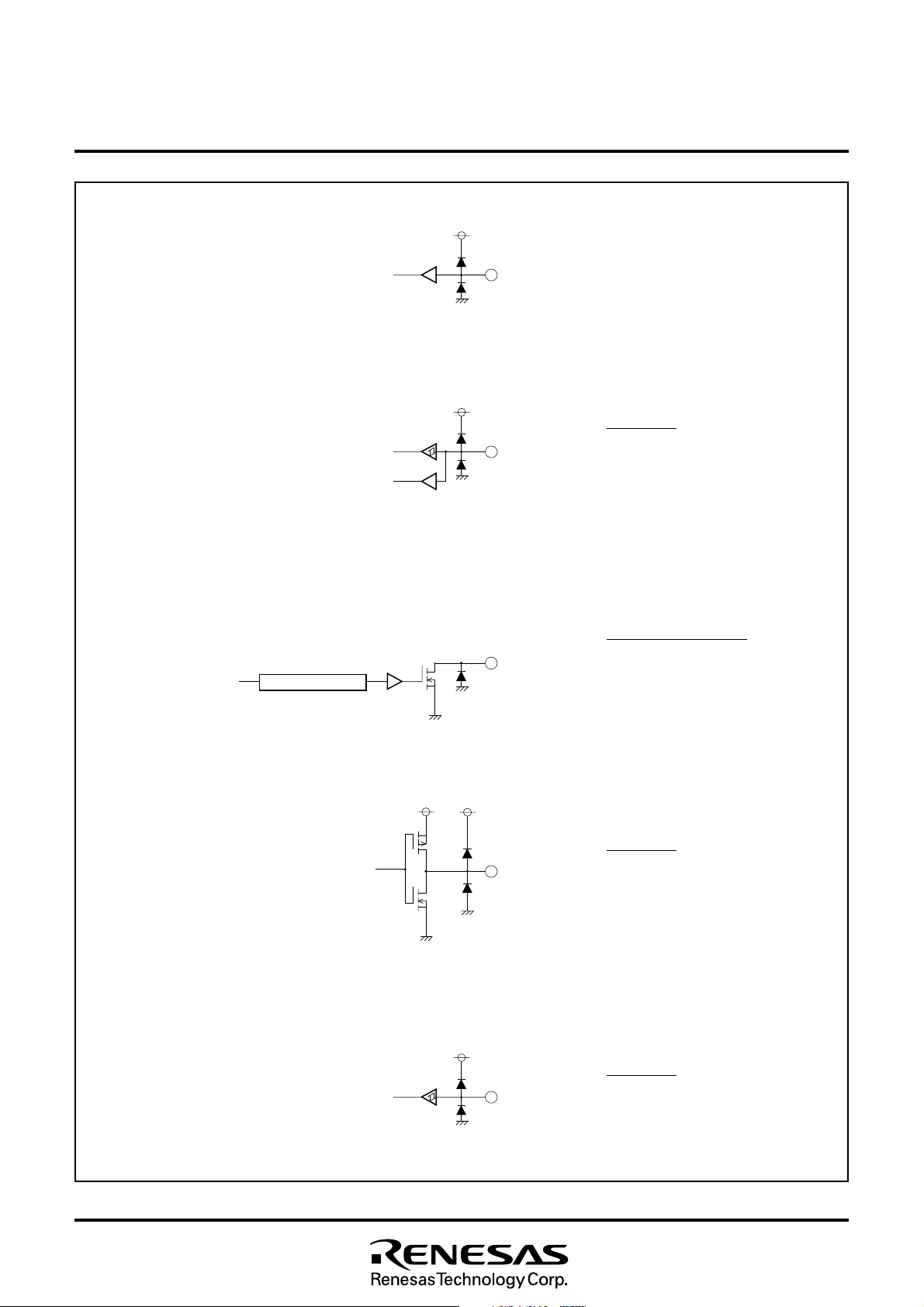
P52/R, Output port P5 Output Ports P52–P55 are a 4-bit output port and has basically the same functions as port P0. The
P53/G,
P54/B,
P55/OUT1 structure is CMOS output.
P60PWM0–
P63/PWM3
HSYNC HSYNC input Input This is a horizontal synchronizing signal input for OSD.
VSYNC VSYNC input Input This is a vertical synchronizing signal input for OSD.
DA DA output Output This is a 14-bit PWM output pin.
Note : Port Pi (i = 0 to 3) has the port Pi direction register which can be used to program each bit as an input (“0”) or an output (“1”). The pins programmed as “1” in
I/O port P4 I/O Ports P40, P41 are a 2-bit I/O port and has basically the same functions as port P0. The
Serial I/O synchronizing
clock input/output structure is N-channel open-drain output.
Analog input pin Input Pin P40, P41 are also used as analog input pins A-D7, A-D6 respectively.
input
Analog input Input Pin P42 is also used as analog input pin A-D5.
OSD output Output Pins P52–P55 are also used as OSD output pins R, G, B, OUT1 respectively. The output
Output port P6 Output Ports P60–P63 are a 4-bit I/O port and has basically the same functions as port P0. The
PWM output Output Pins P60–P63 are also used as PWM output pins PWM0–PWM3 respectively. The output
the direction register are output pins. When pins are programmed as “0,” they are input pins. When pins are programmed as output pins, the output data are
written into the port latch and then output. When data is read from the output pins, the output pin level is not read but the data of the port latch is read. This
allows a previously-output value to be read correctly even if the output “L” voltage has risen, for example, because a light emitting diode was directly driven.
The input pins are in the floating state, so the values of the pins can be read. When data is written into the input pin, it is written only into the port latch, while
the pin remains in the floating state.
Input/
Output
I/O Pin P41 is also used as serial I/O synchronizing clock input/output pin S CLK. The output
output structure is CMOS output.
output structure is N-channel open-drain output.
structure is N-channel open-drain output.
Functions
Rev. 1.0
9
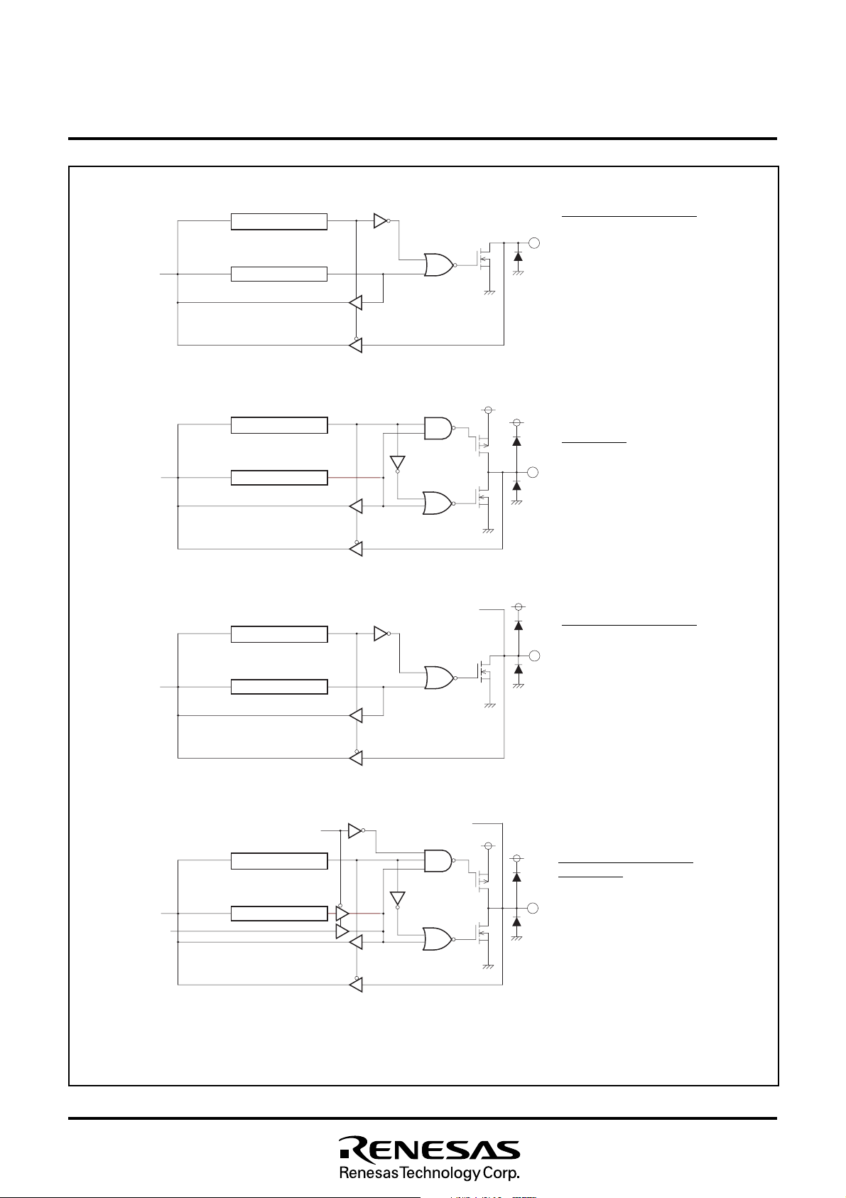
Port P0
MITSUBISHI MICROCOMPUTERS
M37212M4/M8–XXXSP, M37212M6–XXXSP/FP
M37212EFSP/FP
SINGLE-CHIP 8-BIT CMOS MICROCOMPUTER for VOLTAGE SYNTHESIZER
with ON-SCREEN DISPLAY CONTROLLER
N-channel open-drain output
Direction register
Port P0
Data bus
Ports P10, P2, P30, P3
Data bus
Ports P4
0, P41
Data bus
1
Port latch
Direction register
Port latch
Direction register
Port latch
SIN, S
CLK
Note :Each port is also used as follows :
P00–P03 : PWM4–PWM7
CMOS output
Ports P10, P2, P30, P31
Note :Port P10 is also used as OUT2/
A-D8.
N-channel open-drain output
Ports P40, P41
Note :Each port is also used as follows :
P40 : SOUT(/IN)/A-D7
P41 : SCLK/A-D6
Ports P11–P1
Data bus
I2C-BUS clock
2
I
C-BUS data
4
Fig. 7.1 I/O Pin Block Diagram (1)
10
BSEL0
BSEL1
Direction register
Port latch
SCL1, SCL2,
SDA1, SDA2
N-channel open-drain output
CMOS output
Ports P11–P14
Notes 1: Each port is also used as follows :
P11 : SCL1
P12 : SCL2
P13 : SDA1
P14 : SDA2
2: The output structure of ports P11–
P14 is N-channel open-drain output
when using as multi-master I2CBUS interface (it is the same with
ports P40 and P41).
Rev. 1.0
Ports P1
6
, P1
MITSUBISHI MICROCOMPUTERS
M37212M4/M8–XXXSP, M37212M6–XXXSP/FP
M37212EFSP/FP
SINGLE-CHIP 8-BIT CMOS MICROCOMPUTER for VOLTAGE SYNTHESIZER
with ON-SCREEN DISPLAY CONTROLLER
7
Ports P1
5
, P32–P37, P4
Ports P60–P6
Data bus
Data bus
2
TIM2, TIM3,
INT1,
IN
INT2, S
3
Port latch
, INT3
Data bus
Ports P16, P17
Note : Each port is also used as follows :
P16 : A-D2
P17 : A-D3
Schmidt input
Ports P15, P32–P37, P42
Note : Each port is also used as follows :
P15 : INT3/A-D1
P32 : TIM2
P33 : TIM3
P34 : INT1
P35 : INT2/A-D4
P36 : OSC1
P37 : OSC2
P42 : SIN/A-D5
N-chanel open drain output
Ports P60–P63
Note :Each port is also used as follows :
P60–P63 : PWM0–PWM3
D-A, R, G, B, OUT1 , OUT2
H
SYNC
, V
SYNC
Fig. 7.2 I/O Pin Block Diagram (2)
Rev. 1.0
Internal circuit
Internal circuit
CMOS output
Ports D-A, R, G, B, OUT1, OUT2
Note : Each pin is also used as follows :
R : P52
G : P53
B : P54
OUT1 : P55
OUT2 : P10/A-D8
Schmidt input
Ports HSYNC, VSYNC
11
MITSUBISHI MICROCOMPUTERS
0
0
W
W
M37212M4/M8–XXXSP, M37212M6–XXXSP/FP
M37212EFSP/FP
SINGLE-CHIP 8-BIT CMOS MICROCOMPUTER for VOLTAGE SYNTHESIZER
with ON-SCREEN DISPLAY CONTROLLER
8. FUNCTIONAL DESCRIPTION
8.1 CENTRAL PROCESSING UNIT (CPU)
This microcomputer uses the standard 740 Family instruction set.
Refer to the table of 740 Family addressing modes and machine
instructions or the SERIES 740 <Software> User’s Manual for details on the instruction set.
Machine-resident 740 Family instructions are as follows:
The FST, SLW instruction cannot be used.
The MUL, DIV, WIT and STP instructions can be used.
C P U M o d e R e g i s t e r
b 7b 6b 5b 4b 3 b 2b 1b 0
1
1
111
C P U m o d e r e g i s t e r ( C M ) [ A d d r e s s 0 0 F B
B
0 , 1
S t a c k p a g e s e l e c t i o n
2
b i t ( C M 2 ) ( S e e n o t e )
N a m eF
F i x t h e s e b i t s t o “ 0 . ”
8.1.1 CPU Mode Register
The CPU mode register contains the stack page selection bit and
internal system clock selection bit. The CPU mode register is allocated at address 00FB16.
1 6
]
u n c t i o n
0 : 0 p a g e
1 : 1 p a g e
s
A f t e r r e s e t
I n d e t e r m i n a t e
1
RW
R
RW
Fig. 8.1.1 CPU Mode Register
F i x t h e s e b i t s t o “ 1 . ”
3 t o 7
N o t e : T h i s b i t i s s e t t o “ 1 ” a f t e r t h e r e s e t r e l e a s e .
I n d e t e r m i n a t e
R
Rev. 1.0
12
M37212M4/M8–XXXSP, M37212M6–XXXSP/FP
SINGLE-CHIP 8-BIT CMOS MICROCOMPUTER for VOLTAGE SYNTHESIZER
8.2 MEMORY
8.2.1 Special Function Register (SFR) Area
The special function register (SFR) area in the zero page contains
control registers such as I/O ports and timers.
8.2.2 RAM
RAM is used for data storage and for stack area of subroutine calls
and interrupts.
MITSUBISHI MICROCOMPUTERS
M37212EFSP/FP
with ON-SCREEN DISPLAY CONTROLLER
8.2.7 Zero Page
The 256 bytes from addresses 000016 to 00FF16 are called the zero
page area. The internal RAM and the special function registers (SFR)
are allocated to this area.
The zero page addressing mode can be used to specify memory and
register addresses in the zero page area. Access to this area with
only 2 bytes is possible in the zero page addressing mode.
8.2.3 ROM
ROM is used for storing user programs as well as the interrupt vector
area.
8.2.4 OSD RAM
RAM for display is used for specifying the character codes and colors to display.
8.2.5 OSD ROM
ROM for display is used for storing character data.
8.2.6 Interrupt Vector Area
The interrupt vector area contains reset and interrupt vectors.
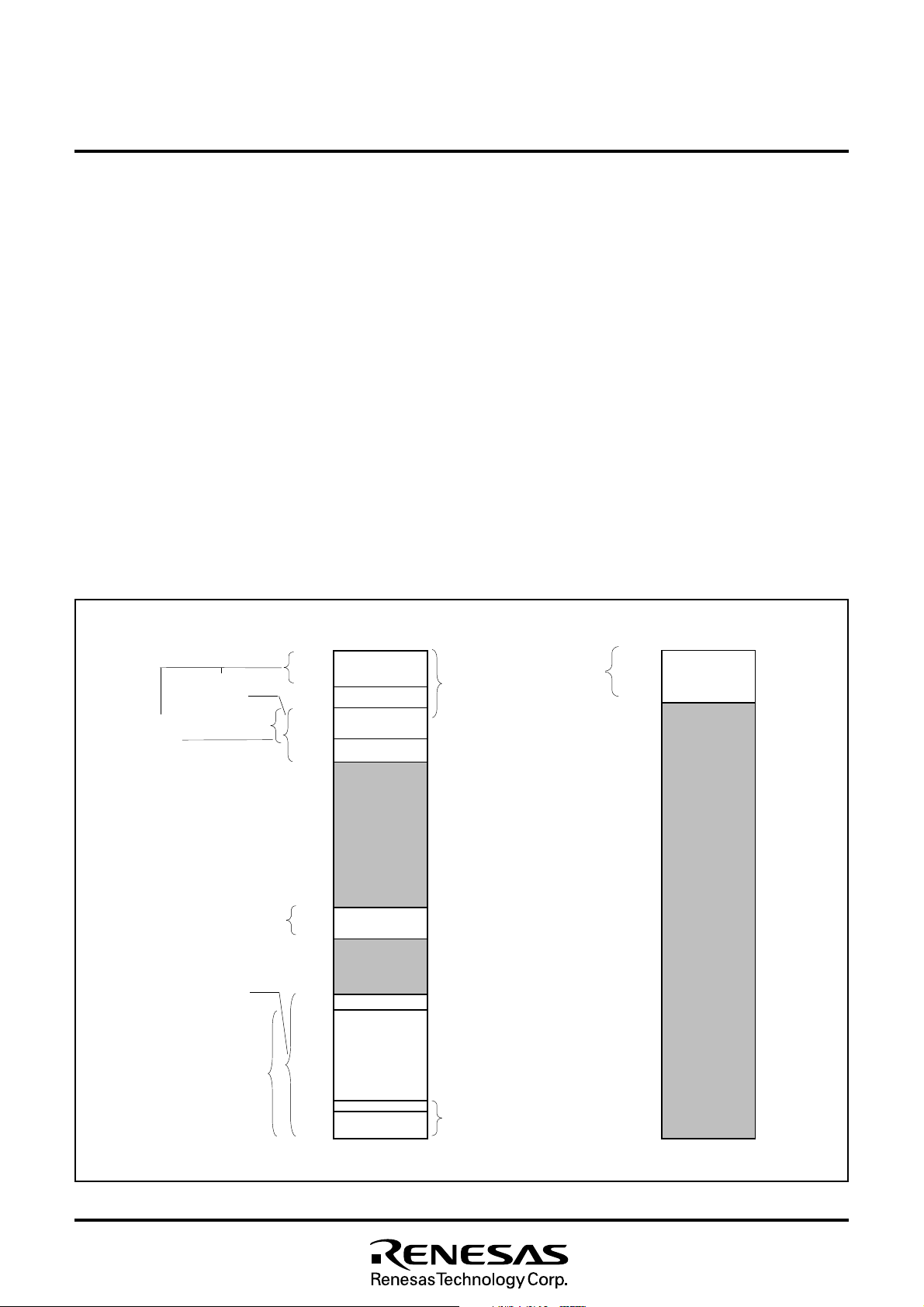
■ M 3 7 2 1 2 M 4 / M 8 - X X X S P , M 3 7 2 1 2 M 6 - X X X S P / F P
0 0 0 0
1 6
M 3 7 2 1 2 M 4 -
X X X S P
R A M
( 3 2 0 b y t e s )
M 3 7 2 1 2 M 6 -
X X X S P / F P
R A M
( 3 8 4 b y t e s )
0 0 B F
0 0 C 0
0 0 F F
0 1 0 0
0 1 7 F
0 1 B F
1 6
1 6
S F R a r e a
1 6
1 6
1 6
1 6
8.2.8 Special Page
The 256 bytes from addresses FF0016 to FFFF16 are called the special page area. The special page addressing mode can be used to
specify memory addresses in the special page area. Access to this
area with only 2 bytes is possible in the special page addressing
mode.
8.2.9 ROM Correction Memory (RAM)
This is used as the program area for ROM correction.
Note: Only M37212M8-XXXSP and M37212EFSP/FP have ROM correction
memory.
1 0 0 0 0
Z e r o p a g e
O S D R O M
( 8 K b y t e s )
1 1 F F F
1 6
1 6
N o t u s e d
M 3 7 2 1 2 M 6 -
X X X S P / F P
R O M
( 2 4 K b y t e s )
M 3 7 2 1 2 M 4 -
X X X S P
R O M
( 1 6 K b y t e s )
O S D R A M
( 9 6 b y t e s )
( S e e n o t e )
0 6 0 0
0 6 B 7
A 0 0 0
C 0 0 0
F F 0 0
F F D E
F F F F
1 6
1 6
1 6
1 6
1 6
1 6
I n t e r r u p t v e c t o r a r e a
1 6
N o t u s e d
S p e c i a l p a g e
Fig. 8.2.1 Memory Map (M37212M4/M8-XXXSP, M37212M6-XXXSP/FP)
Rev. 1.0
N o t u s e d
1 F F F F
1 6
N o t e : R e f e r t o T a b l e 8 . 1 0 . 3 O S D R A M .
13
M37212M4/M8–XXXSP, M37212M6–XXXSP/FP
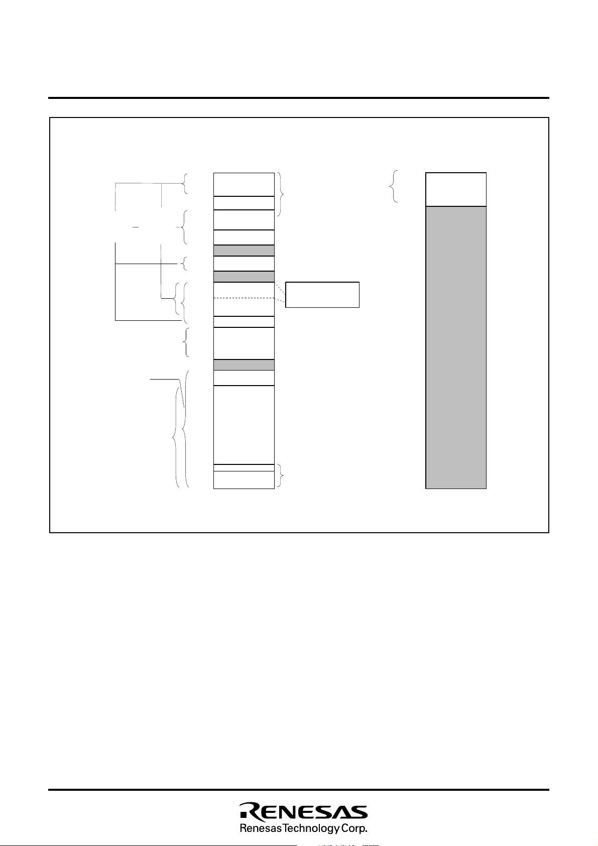
■ M 3 7 2 1 2 M 8 - X X X S P , M 3 7 2 1 2 E F S P / F P
0 0 0 0
1 6
0 0 B F
1 6
0 0 C 0
1 6
0 0 F F
M 3 7 2 1 2 E F S P
R A M
( 1 2 8 0 b y t e s )
M 3 7 2 1 2 E F S P
( 6 2 K b y t e s )
R O M
M 3 7 2 1 2 M 8 -
X X X S P
R A M
( 5 7 6 b y t e s )
O S D R A M
( 9 6 b y t e s )
( S e e n o t e )
0 1 0 0
0 1 F F
0 2 1 7
0 2 1 B
0 2 C 0
0 2 E 0
0 3 3 F
0 5 F F
0 6 0 0
0 6 B 7
0 8 0 0
8 0 0 0
1 6
1 6
1 6
1 6
1 6
1 6
1 6
1 6
1 6
1 6
1 6
1 6
1 6
MITSUBISHI MICROCOMPUTERS
M37212EFSP/FP
SINGLE-CHIP 8-BIT CMOS MICROCOMPUTER for VOLTAGE SYNTHESIZER
with ON-SCREEN DISPLAY CONTROLLER
1 0 0 0 0
S F R a r e a
N o t u s e d
2 p a g e r e g i s t e r
N o t u s e d
N o t u s e d
Z e r o p a g e
R O M c o r r e c t i o n f u n c t i o n
V e c t o r 1 : a d d r e s s 0 2 C 0
V e c t o r 2 : a d d r e s s 0 2 E 0
O S D R O M
( 8 K b y t e s )
1 6
1 6
1 1 F F F
1 6
1 6
N o t u s e d
M 3 7 2 1 2 M 8 -
X X X S P
R O M
( 3 2 K b y t e s )
F F 0 0
1 6
F F D E
1 6
I n t e r r u p t v e c t o r a r e a
F F F F
1 6
Fig. 8.2.2 Memory Map (M37212M8-XXXSP, M37212EFSP/FP)
S p e c i a l p a g e
1 F F F F
1 6
N o t e : R e f e r t o T a b l e 8 . 1 0 . 3 O S D R A M
14
Rev. 1.0
MITSUBISHI MICROCOMPUTERS
K
M37212M4/M8–XXXSP, M37212M6–XXXSP/FP
M37212EFSP/FP
SINGLE-CHIP 8-BIT CMOS MICROCOMPUTER for VOLTAGE SYNTHESIZER
with ON-SCREEN DISPLAY CONTROLLER
■ S F R a r e a ( a d d r e s s e s C 0
A d d r e s s
C 0
1 6
C 1
1 6
C 2
1 6
C 3
1 6
C 4
1 6
C 5
1 6
C 6
1 6
C 7
1 6
C 8
1 6
C 9
1 6
C A
1 6
C B
1 6
C C
1 6
C D
1 6
C E
1 6
C F
1 6
D 0
1 6
D 1
1 6
D 2
1 6
D 3
1 6
D 4
1 6
D 5
1 6
D 6
1 6
D 7
1 6
D 8
1 6
D 9
1 6
D A
1 6
D B
1 6
D C
1 6
D D
1 6
D E
1 6
D F
1 6
R e g i s t e r
P o r t P 0 ( P 0 )
P o r t P 0 d i r e c t i o n r e g i s t e r ( D 0 )
P o r t P 1 ( P 1 )
P o r t P 1 d i r e c t i o n r e g i s t e r ( D 1 )
P o r t P 2 ( P 2 )
P o r t P 2 d i r e c t i o n r e g i s t e r ( D 2 )
P o r t P 3 ( P 3 )
P o r t P 3 d i r e c t i o n r e g i s t e r ( D 3 )
P o r t P 4 ( P 4 )
P o r t P 4 d i r e c t i o n r e g i s t e r ( D 4 )
P o r t P 5 ( P 5 )
P o r t P 5 d i r e c t i o n r e g i s t e r ( D 5 )
P o r t P 6 ( P 6 )
D A - H r e g i s t e r ( D A - H )
D A - L r e g i s t e r ( D A - L )
P W M 0 r e g i s t e r ( P W M 0 )
P W M 1 r e g i s t e r ( P W M 1 )
P W M 2 r e g i s t e r ( P W M 2 )
P W M 3 r e g i s t e r ( P W M 3 )
P W M 4 r e g i s t e r ( P W M 4 )
P W M o u t p u t c o n t r o l r e g i s t e r 1 ( P W )
P W M o u t p u t c o n t r o l r e g i s t e r 2 ( P N )
2
I
C d a t a s h i f t r e g i s t e r ( S 0 )
2
C a d d r e s s r e g i s t e r ( S 0 D )
I
I2C s t a t u s r e g i s t e r ( S 1 )
I2C c o n t r o l r e g i s t e r ( S 1 D )
2
I
C c l o c k c o n t r o l r e g i s t e r ( S 2 )
S e r i a l I / O m o d e r e g i s t e r ( S M )
S e r i a l I / O r e g i s t e r ( S I O )
1 6
t o D F
1 6
)
B i t a l l o c a t i o n
:
F u n c t i o n b i t
:
N a m e
:
N o f u n c t i o n b i t
: F i x t o t h i s b i t t o “ 0 ”
0
( d o n o t w r i t e t o “ 1 ” )
: F i x t o t h i s b i t t o “ 1 ”
1
( d o n o t w r i t e t o “ 0 ” )
B i t a l l o c a t i o n S t a t e i m m e d i a t e l y a f t e r r e s e t
b 7
P 5 4
P 5 5
S E L
S E L
A
1 0 B I T
B S E L 0B S E L 1
S
A C K
B I T
F A S T
M O D E
D
A C
0
P 5 3
S E L
P 6 3
S t a t e i m m e d i a t e l y a f t e r r e s e t
: “ 0 ” i m m e d i a t e l y a f t e r r e s e t
0
: “ 1 ” i m m e d i a t e l y a f t e r r e s e t
1
: I n d e t e r m i n a t e i m m e d i a t e l y
?
a f t e r r e s e t
b 0
b 7
P 3 1 DP 3 0 D
P 5 2P 5 3P 5 4P 5 5
P 5 2
S E L
P 4 1P 4 0
P 4 1 DP 4 0 D
00
P 6 1P 6 0P 6 2
0
0
0
0
0????00
0
1111
00
P W 0P W 1P W 2P W 3P W 4P W 5P W 6P W 7
P N 2P N 3P N 4
P N 0P N 1
D 1D 2D 3D 4D 5D 6D 7D
0
S A D 0S A D 1S A D 2S A D 3S A D 4S A D 5S A D 6
R B W
L R BA D 0A A SA LP I NB BT R XM S T
B C 0B C 1B C 2E S OA L S
C C R 0C C R 1C C R 2C C R 3C C R 4
S M 0S M 1S M 2S M 3S M 5S M 6
00
b 0
?
1 6
0 0
?
1 6
0 0
?
0 0
1 6
?
0 0
1 6
00
00
0 0
0 F
0 F
1 6
1 6
1 6
?0
?0
??
??
?
??????
?
?
?
?
?
1 6
0 0
0 0
1 6
?
0 0
1 6
?00010
0 0
1 6
0 0
1 6
0 0
1 6
?
?
?
Fig. 8.2.3 Memory Map of Special Function Register (SFR) (1)
Rev. 1.0
15
MITSUBISHI MICROCOMPUTERS
6
M37212M4/M8–XXXSP, M37212M6–XXXSP/FP
M37212EFSP/FP
SINGLE-CHIP 8-BIT CMOS MICROCOMPUTER for VOLTAGE SYNTHESIZER
with ON-SCREEN DISPLAY CONTROLLER
■ S F R a r e a ( a d d r e s s e s E 0
A d d r e s s
E 0
1 6
E 1
1 6
E 2
1 6
E 3
1 6
E 4
1 6
E 5
1 6
E 6
1 6
E 7
1
E 8
1 6
E 9
1 6
E A
1 6
E B
1 6
E C
1 6
E D
1 6
E E
1 6
E F
1 6
F 0
1 6
F 1
1 6
F 2
1 6
F 3
1 6
F 4
1 6
F 5
1 6
F 6
1 6
F 7
1 6
F 8
1 6
F 9
1 6
F A
1 6
F B
1 6
F C
1 6
F D
1 6
F E
1 6
F F
1 6
R e g i s t e r
H o r i z o n t a l p o s i t i o n r e g i s t e r ( H R )
V e r t i c a l p o s i t i o n r e g i s t e r 1 ( C V 1 )
V e r t i c a l p o s i t i o n r e g i s t e r 2 ( C V 2 )
C h a r a c t e r s i z e r e g i s t e r ( C S )
B o r d e r s e l e c t i o n r e g i s t e r ( M D )
C o l o r r e g i s t e r 0 ( C O 0 )
C o l o r r e g i s t e r 1 ( C O 1 )
C o l o r r e g i s t e r 2 ( C O 2 )
C o l o r r e g i s t e r 3 ( C O 3 )
C R T c o n t r o l r e g i s t e r ( C C )
C R T p o r t c o n t r o l r e g i s t e r ( C R T P )
C R T c l o c k s e l e c t i o n r e g i s t e r ( C K )
A - D m o d e r e g i s t e r ( A D M )
A - D c o n t r o l r e g i s t e r ( A D C )
T i m e r 1 ( T 1 )
T i m e r 2 ( T 2 )
T i m e r 3 ( T 3 )
T i m e r 4 ( T 4 )
T i m e r 1 2 m o d e r e g i s t e r ( T 1 2 M )
T i m e r 3 4 m o d e r e g i s t e r ( T 3 4 M )
P W M 5 r e g i s t e r ( P W M 5 )
P W M 6 r e g i s t e r ( P W M 6 )
P W M 7 r e g i s t e r ( P W M 7 )
I n t e r r u p t i n p u t p o l a r i t y r e g i s t e r ( R E )
C P U m o d e r e g i s t e r ( C M )
I n t e r r u p t r e q u e s t r e g i s t e r 1 ( I R E Q 1 )
n t e r r u p t r e q u e s t r e g i s t e r 2 ( I R E Q 2
I
I n t e r r u p t c o n t r o l r e g i s t e r 1 ( I C O N 1 )
n t e r r u p t c o n t r o l r e g i s t e r 2 ( I C O N 2
I
1 6
t o F F
1 6
)
B i t a l l o c a t i o n
:
F u n c t i o n b i t
:
N a m e
:
N o f u n c t i o n b i t
: F i x t o t h i s b i t t o “ 0 ”
0
( d o n o t w r i t e t o “ 1 ” )
: F i x t o t h i s b i t t o “ 1 ”
1
( d o n o t w r i t e t o “ 0 ” )
B i t a l l o c a t i o nS
b 7
C C 7
O P 7
00
0000
0
R E5
1111
O S D R
V S C RI T 3 R
I I C R
)
0
I I C E
)
00
C K 0M S R
O S D E
V S C EI T 3 E
0
S t a t e i m m e d i a t e l y a f t e r r e s e t
: “ 0 ” i m m e d i a t e l y a f t e r r e s e t
0
: “ 1 ” i m m e d i a t e l y a f t e r r e s e t
1
: I n d e t e r m i n a t e i m m e d i a t e l y
?
a f t e r r e s e t
t a t e i m m e d i a t e l y a f t e r r e s e
b 0
b 7
H R 0H R 1H R 2H R 3H R 4H R 5
C V 1 1C V 1 2C V 1 3C V 1 4C V 1 5C V 1 6
C V 1 0
C V 2 0C V 2 1C V 2 2C V 2 3C V 2 4C V 2 5C V 2 6
0 0
??? ????0
??? ????0
0 0
C S 1 0C S 1 1C S 2 0C S 2 1
M D 1 0M D 2 0
C O 0 1C O 0 2C O 0 3C O 0 5C O 0 4C O 0 6C O 0 7
C O 1 1C O 1 2C O 1 3C O 1 5C O 1 4C O 1 6C O 1 7
C O 2 1C O 2 2C O 2 3C O 2 5C O 2 4C O 2 6C O 2 7
C O 3 1C O 3 2C O 3 3C O 3 5C O 3 4C O 3 6C O 3 7
C C 0C C 1C C 2
S Y
V S Y CR / G / BO U T 2O P 5 O U T 1O P 6H
A D M1A D M2A D M4
A D C1A D C2A D C3A D C4A D C5
C
C K0C K1
A D M0
A D C0
000 ????0
000 0?0?0
0 0
0 0
0 0
0 0
0 0
0 0
0 0
0 0
?00 00000
0 0
F F
0 7
F F
0 7
T 1 2 M 0T 1 2 M 1T 1 2 M 2T 1 2 M 3T 1 2 M 4
T 3 4 M 0
T 3 4 M 1T 3 4 M 2T 3 4 M 3T 3 4 M 4T 3 4 M 5
0 0
0 0
1 6
1 6
1 6
1 6
1 6
1 6
1 6
1 6
1 6
1 6
1 6
1 6
1 6
1 6
1 6
1 6
1 6
t
b 0
?
?
?
R E3R E4
00
0 0
1 6
?
C M 2
S 1 R
S 1 EM S E
001
T M 1 RT M 2 RT M 3 RT M 4 R
I T 1 RI T 2 R
T M 1 ET M 2 ET M 3 ET M 4 E
I T 1 EI T 2 E
?00 00000
FC
0 0
0 0
0 0
1 6
1 6
1 6
1 6
Fig. 8.2.4 Memory Map of Special Function Register (SFR) (2)
Rev. 1.0
16
M37212M4/M8–XXXSP, M37212M6–XXXSP/FP
SINGLE-CHIP 8-BIT CMOS MICROCOMPUTER for VOLTAGE SYNTHESIZER
t o 2 1
■ 2 p a g e r e g i s t e r a r e a ( a d d r e s s e s 2 1 71
< B i t a l l o c a t i o n ><
:
F u n c t i o n b i t
:
N a m e
o f u n c t i o n b i
: N
: F i x t o t h i s b i t t o “ 0 ”
0
( d o n o t w r i t e t o “ 1 ” )
: F i x t o t h i s b i t t o “ 1 ”
1
( d o n o t w r i t e t o “ 0 ” )
A d d r e s s
2 1 71
6
2 1 81
6
2 1 91
6
2 1 A1
6
2 1 B1
6
R e g i s t e r
R O M c o r r e c t i o n a d d r e s s 1 ( h i g h - o r d e r )
O M c o r r e c t i o n a d d r e s s 1 ( l o w - o r d e r
R
R O M c o r r e c t i o n a d d r e s s 2 ( h i g h - o r d e r )
O M c o r r e c t i o n a d d r e s s 2 ( l o w - o r d e r
R
R O M c o r r e c t i o n e n a b l e r e g i s t e r ( R C R )
b 7b
)
)
B i t a l l o c a t i o nS
6
MITSUBISHI MICROCOMPUTERS
with ON-SCREEN DISPLAY CONTROLLER
B1
6)
S t a t e i m m e d i a t e l y a f t e r r e s e t
0
1
t
?
t a t e i m m e d i a t e l y a f t e r r e s e
0b
7b
R C R 1R C R 0
00 0 01
M37212EFSP/FP
: “ 0 ” i m m e d i a t e l y a f t e r r e s e t
: “ 1 ” i m m e d i a t e l y a f t e r r e s e t
: I n d e t e r m i n a t e i m m e d i a t e l y
a f t e r r e s e t
0 01
6
0 01
6
0 01
6
0 01
6
6
>
t
0
N o t e : O n l y M 3 7 2 1 2 M 8 - X X X S P a n d M 3 7 2 1 2 E F S P / F P h a v e 2 p a g e r e g i s t e r .
Fig. 8.2.5 Memory Map of 2 Page Register Area
Rev. 1.0
17
MITSUBISHI MICROCOMPUTERS
M37212M4/M8–XXXSP, M37212M6–XXXSP/FP
M37212EFSP/FP
SINGLE-CHIP 8-BIT CMOS MICROCOMPUTER for VOLTAGE SYNTHESIZER
with ON-SCREEN DISPLAY CONTROLLER
< B i t a l l o c a t i o n ><
:
F u n c t i o n b i t
:
N a m e
:
N o f u n c t i o n b i t
: F i x t o t h i s b i t t o “ 0 ”
0
( d o n o t w r i t e t o “ 1 ” )
: F i x t o t h i s b i t t o “ 1 ”
1
( d o n o t w r i t e t o “ 0 ” )
R e g i s t e r
b 7
P r o c e s s o r s t a t u s r e g i s t e r ( P S )
P r o g r a m c o u n t e r ( P CH)
P r o g r a m c o u n t e r ( P CL)
Fig. 8.2.6 Internal State of Processor Status Register and Program Counter at Reset
B i t a l l o c a t i o nS
b 0
I Z CDBTVN???????
S t a t e i m m e d i a t e l y a f t e r r e s e t
: “ 0 ” i m m e d i a t e l y a f t e r r e s e t
0
: “ 1 ” i m m e d i a t e l y a f t e r r e s e t
1
: I n d e t e r m i n a t e i m m e d i a t e l y
?
a f t e r r e s e t
t a t e i m m e d i a t e l y a f t e r r e s e
b 7
1
C o n t e n t s o f a d d r e s s F F F F
C o n t e n t s o f a d d r e s s F F F E
>
t
b 0
1 6
1 6
18
Rev. 1.0
MITSUBISHI MICROCOMPUTERS
M37212M4/M8–XXXSP, M37212M6–XXXSP/FP
M37212EFSP/FP
SINGLE-CHIP 8-BIT CMOS MICROCOMPUTER for VOLTAGE SYNTHESIZER
with ON-SCREEN DISPLAY CONTROLLER
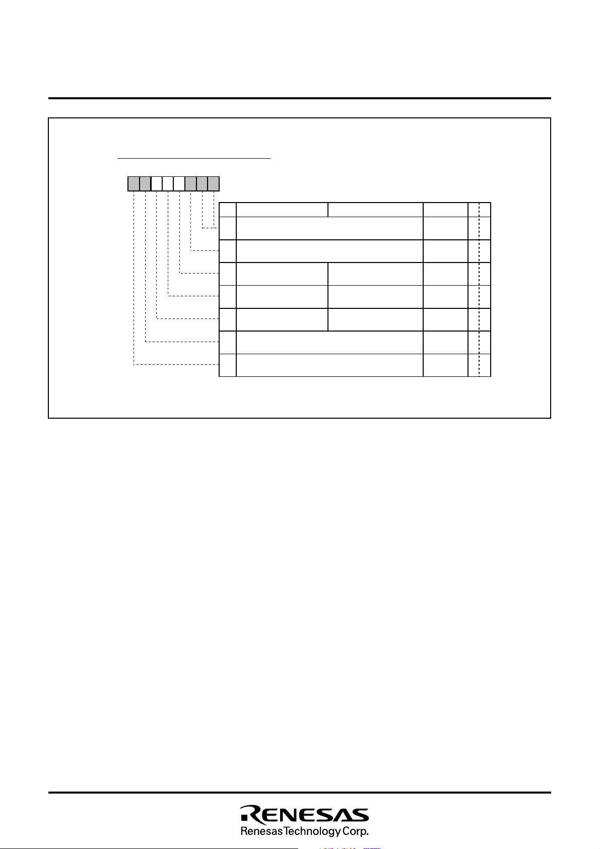
8.3 INTERRUPTS
Interrupts can be caused by 14 different sources consisting of 4 external, 8 internal, 1 software, and reset. Interrupts are vectored interrupts with priorities as shown in Table 8.3.1. Reset is also included in
the table because its operation is similar to an interrupt.
When an interrupt is accepted,
① The contents of the program counter and processor status regis-
ter are automatically stored into the stack.
➁ The interrupt disable flag I is set to “1” and the corresponding
interrupt request bit is set to “0.”
➂ The jump destination address stored in the vector address enters
the program counter.
Other interrupts are disabled when the interrupt disable flag is set to
“1.”
All interrupts except the BRK instruction interrupt have an interrupt
request bit and an interrupt enable bit. The interrupt request bits are
in interrupt request registers 1 and 2 and the interrupt enable bits are
in interrupt control registers 1 and 2. Figures 8.3.2 to 8.3.6 show the
interrupt-related registers.
Interrupts other than the BRK instruction interrupt and reset are accepted when the interrupt enable bit is “1,” interrupt request bit is “1,”
and the interrupt disable flag is “0.” The interrupt request bit can be
set to “0” by a program, but not set to “1.” The interrupt enable bit can
be set to “0” and “1” by a program.
Reset is treated as a non-maskable interrupt with the highest priority.
Figure 8.3.1 shows interrupt control.
8.3.1 Interrupt Causes
SYNC, OSD interrupts
(1) V
The VSYNC interrupt is an interrupt request synchronized with
the vertical sync signal.
The OSD interrupt occurs after character block display to the
CRT is completed.
(2) INT1 to INT3 external interrupts
The INT1 to INT3 interrupts are external interrupt inputs, the system detects that the level of a pin changes from LOW to HIGH or
from HIGH to LOW, and generates an interrupt request. The input active edge can be selected by bits 3 to 5 of the interrupt
input polarity register (address 00F916) : when this bit is “0,” a
change from LOW to HIGH is detected; when it is “1,” a change
from HIGH to LOW is detected. Note that both bits are cleared to
“0” at reset.
(3) Timers 1 to 4 interrupts
An interrupt is generated by an overflow of timers 1 to 4.
Table 8.3.1 Interrupt Vector Addresses and Priority
Priority
1
2
3
4
5
6
7
8
9
10
11
12
13
14
Reset
OSD interrupt
INT2 external interrupt
INT1 external interrupt
Timer 4 interrupt
f(XIN)/4096 interrupt
VSYNC interrupt
Timer 3 interrupt
Timer 2 interrupt
Timer 1 interrupt
Serial I/O interrupt
Multi-master I2C-BUS interface interrupt
INT3 external interrupt
BRK instruction interrupt
Interrupt Source
Vector Addresses
FFFF16, FFFE16
FFFD16, FFFC16
FFFB16, FFFA16
FFF916, FFF816
FFF516, FFF416
FFF316, FFF216
FFF116, FFF016
FFEF16, FFEE16
FFED16, FFEC16
FFEB16, FFEA16
FFE916, FFE816
FFE716, FFE616
FFE516, FFE416
FFDF16, FFDE16
Remarks
Non-maskable
Active edge selectable
Active edge selectable
Active edge selectable
Non-maskable
Rev. 1.0
19
M37212M4/M8–XXXSP, M37212M6–XXXSP/FP
t
SINGLE-CHIP 8-BIT CMOS MICROCOMPUTER for VOLTAGE SYNTHESIZER
(4) Serial I/O interrupt
This is an interrupt request from the clock synchronous serial I/O
function.
MITSUBISHI MICROCOMPUTERS
M37212EFSP/FP
with ON-SCREEN DISPLAY CONTROLLER
(5) f(XIN)/4096 interrupt
The f (XIN)/4096 interrupt occurs regularly with a f(XIN)/4096 period. Set bit 0 of PWM output control register 1 to “0.”
(6) Multi-master I2C-BUS interface interrupt
This is an interrupt request related to the multi-master I2C-BUS
interface.
(7) BRK instruction interrupt
This software interrupt has the least significant priority. It does
not have a corresponding interrupt enable bit, and it is not affected by the interrupt disable flag I (non-maskable).
Interrupt request bi
Interrupt enable bit
Interrupt disable flag I
Fig. 8.3.1 Interrupt Control
BRK instruction
Reset
Interrupt
request
20
Rev. 1.0
M37212M4/M8–XXXSP, M37212M6–XXXSP/FP
e
6
e
W
I n t e r r u p t R e q u e s t R e g i s t e r 1
b 7b 6 b 5b 4b 3 b 2b 1b 0
I n t e r r u p t r e q u e s t r e g i s t e r 1 ( I R E Q 1 ) [ A d d r e s s 0 0 F C
MITSUBISHI MICROCOMPUTERS
M37212EFSP/FP
SINGLE-CHIP 8-BIT CMOS MICROCOMPUTER for VOLTAGE SYNTHESIZER
with ON-SCREEN DISPLAY CONTROLLER
1 6
]
Fig. 8.3.2 Interrupt Request Register 1
BN
0
T i m e r 1 i n t e r r u p t
r e q u e s t b i t ( T M 1 R )
1
2
3T i m e r 4 i n t e r r u p t
4
5
6
7
a m
T i m e r 2 i n t e r r u p t
r e q u e s t b i t ( T M 2 R )
T i m e r 3 i n t e r r u p t
r e q u e s t b i t ( T M 3 R )
r e q u e s t b i t ( T M 4 R )
O S D i n t e r r u p t r e q u e s t
b i t ( O S D R )
S Y N C
i n t e r r u p t
V
r e q u e s t b i t ( V S C R )
M u l t i - m a s t e r I2C - B U S i n t e r f a c e
i n t e r r u p t r e q u e s t b i t ( I I C R )
I N T 3 e x t e r n a l i n t e r r u p t
r e q u e s t b i t ( I T 3 R )
F u n c t i o n s
N o i n t e r r u p t r e q u e s t i s s u e d
0 :
1 :
I n t e r r u p t r e q u e s t i s s u e d
N o i n t e r r u p t r e q u e s t i s s u e d
0 :
1 :
I n t e r r u p t r e q u e s t i s s u e d
0 :
N o i n t e r r u p t r e q u e s t i s s u e d
1 :
I n t e r r u p t r e q u e s t i s s u e d
0 :
N o i n t e r r u p t r e q u e s t i s s u e d
1 :
I n t e r r u p t r e q u e s t i s s u e d
0 :
N o i n t e r r u p t r e q u e s t i s s u e d
1 :
I n t e r r u p t r e q u e s t i s s u e d
0 :
N o i n t e r r u p t r e q u e s t i s s u e d
1 :
I n t e r r u p t r e q u e s t i s s u e d
0 :
N o i n t e r r u p t r e q u e s t i s s u e d
1 :
I n t e r r u p t r e q u e s t i s s u e d
0 :
N o i n t e r r u p t r e q u e s t i s s u e d
1 :
I n t e r r u p t r e q u e s t i s s u e d
✽: “ 0 ” c a n b e s e t b y s o f t w a r e , b u t “ 1 ” c a n n o t b e s e t .
A f t e r r e s e t
0
0
0
0 ✽
0
0
0
0
RW
R
✽
R
✽
R
✽
R
✽
R
✽
R
✽
R
✽
R
I n t e r r u p t R e q u e s t R e g i s t e r 2
b 7b
b 5b 4b 3 b 2b 1b 0
0
Fig. 8.3.3 Interrupt Request Register 2
I n t e r r u p t r e q u e s t r e g i s t e r 2 ( I R E Q 2 ) [ A d d r e s s 0 0 F D
BN
0
1
2
3
a m
I N T 1 e x t e r n a l i n t e r r u p t
r e q u e s t b i t ( I T 1 R )
I N T 2 e x t e r n a l i n t e r r u p t
r e q u e s t b i t ( I T 2 R )
S e r i a l I / O i n t e r r u p t
r e q u e s t b i t ( S 1 R )
0 :
1 :
0 :
1 :
0 :
1 :
F u n c t i o n s
N o i n t e r r u p t r e q u e s t i s s u e d
I n t e r r u p t r e q u e s t i s s u e d
N o i n t e r r u p t r e q u e s t i s s u e d
I n t e r r u p t r e q u e s t i s s u e d
N o i n t e r r u p t r e q u e s t i s s u e d
I n t e r r u p t r e q u e s t i s s u e d
N o t h i n g i s a s s i g n e d . T h i s b i t i s a w r i t e d i s a b l e b i t .
W h e n t h i s b i t i s r e a d o u t , t h e v a l u e i s “ 0 . ”
f ( X
I N
4
5 , 6
) / 4 0 9 6 i n t e r r u p t
r e q u e s t b i t ( M S R )
0 :
N o i n t e r r u p t r e q u e s t i s s u e d
1 :
I n t e r r u p t r e q u e s t i s s u e d
N o t h i n g i s a s s i g n e d . T h e s e b i t s a r e w r i t e d i s a b l e b i t s .
W h e n t h e s e b i t s a r e r e a d o u t , t h e v a l u e s a r e “ 0 . ”
F i x t h i s b i t t o “ 0 . ”
7
✽: “ 0 ” c a n b e s e t b y s o f t w a r e , b u t “ 1 ” c a n n o t b e s e t .
1 6
]
A f t e r r e s e t
RW
0
R
✽
0
0
0R
0
0
0
✽
R
✽
R
—
✽
R
—
R
R
Rev. 1.0
21
M37212M4/M8–XXXSP, M37212M6–XXXSP/FP
7
I n t e r r u p t C o n t r o l R e g i s t e r 1
b 7b 6 b 5b 4b 3 b 2b 1b 0
I n t e r r u p t c o n t r o l r e g i s t e r 1 ( I C O N 1 ) [ A d d r e s s 0 0 F E
BN
0
1
2
3
4
5
6
MITSUBISHI MICROCOMPUTERS
M37212EFSP/FP
SINGLE-CHIP 8-BIT CMOS MICROCOMPUTER for VOLTAGE SYNTHESIZER
with ON-SCREEN DISPLAY CONTROLLER
1 6
]
a m
eF
T i m e r 1 i n t e r r u p t
e n a b l e b i t ( T M 1 E )
T i m e r 2 i n t e r r u p t
e n a b l e b i t ( T M 2 E )
T i m e r 3 i n t e r r u p t
e n a b l e b i t ( T M 3 E )
T i m e r 4 i n t e r r u p t
e n a b l e b i t ( T M 4 E )
O S D i n t e r r u p t e n a b l e b i t
( O S D E )
V
S Y N C
i n t e r r u p t e n a b l e
b i t ( V S C E )
n t e r r u p t e n a b l e b i t ( I I C E
M u l t i - m a s t e r I2C - B U S i n t e r f a c e
i
)
I N T 3 e x t e r n a l i n t e r r u p t
e n a b l e b i t ( I T 3 E )
u n c t i o n
s RW
0 : I n t e r r u p t d i s a b l e d
1 : I n t e r r u p t e n a b l e d
0 : I n t e r r u p t d i s a b l e d
1 : I n t e r r u p t e n a b l e d
0 : I n t e r r u p t d i s a b l e d
1 : I n t e r r u p t e n a b l e d
0 : I n t e r r u p t d i s a b l e d
1 : I n t e r r u p t e n a b l e d
0 : I n t e r r u p t d i s a b l e d
1 : I n t e r r u p t e n a b l e d
0 : I n t e r r u p t d i s a b l e d
1 : I n t e r r u p t e n a b l e d
0 : I n t e r r u p t d i s a b l e d
1 : I n t e r r u p t e n a b l e d
0 : I n t e r r u p t d i s a b l e d
1 : I n t e r r u p t e n a b l e d
A f t e r r e s e t
0
0
0
0
0
0
0
0
RW
RW
RW
RW
RW
RW
RW
R
W
Fig. 8.3.4 Interrupt Control Register 1
I n t e r r u p t C o n t r o l R e g i s t e r 2
b 7b 6 b 5b 4b 3 b 2b 1b 0
00
0
I n t e r r u p t c o n t r o l r e g i s t e r 2 ( I C O N 2 ) [ A d d r e s s 0 0 F F
BN
0
a m
eF
I N T 1 e x t e r n a l i n t e r r u p t
e n a b l e b i t ( I T 1 E )
I N T 2 e x t e r n a l i n t e r r u p t
1
e n a b l e b i t ( I T 2 E )
S e r i a l I / O i n t e r r u p t
2
e n a b l e b i t ( S 1 E )
F i x t h i s b i t t o “ 0 . ”
3
f ( X
I N
4
) / 4 0 9 6 i n t e r r u p t
e n a b l e b i t ( M S E )
F i x t h e s e b i t s t o “ 0 . ”
5 , 6
N o t h i n g i s a s s i g n e d . T h e s e b i t s a r e w r i t e d i s a b l e b i t s . W h e n
7
t h e s e b i t s a r e r e a d o u t , t h e v a l u e s a r e “ i n d e t e r m i n a t e . ”
u n c t i o n
s
0 : I n t e r r u p t d i s a b l e d
1 : I n t e r r u p t e n a b l e d
0 : I n t e r r u p t d i s a b l e d
1 : I n t e r r u p t e n a b l e d
0 : I n t e r r u p t d i s a b l e d
1 : I n t e r r u p t e n a b l e d
0 : I n t e r r u p t d i s a b l e d
1 : I n t e r r u p t e n a b l e d
1 6
]
A f t e r r e s e t
0
0
0
0
0
0
i n d e t e r m i n a t e
RW
RW
RW
RW
R
RW
RWW
–
R
Fig. 8.3.5 Interrupt Control Register 2
Rev. 1.0
22
M37212M4/M8–XXXSP, M37212M6–XXXSP/FP
(
s
f
t
W
“
“
WRWRWRW
W
SINGLE-CHIP 8-BIT CMOS MICROCOMPUTER for VOLTAGE SYNTHESIZER
I n t e r r u p t I n p u t P o l a r i t y R e g i s t e r
b 7b 6b 5b 4b 3b 2b 1b 0
00
R E ) [ A d d r e s s 0 0 F
I n t e r r u p t i n p u t p o l a r i t y r e g i s t e r
MITSUBISHI MICROCOMPUTERS
M37212EFSP/FP
with ON-SCREEN DISPLAY CONTROLLER
1 6
]
9
Fig. 8.3.6 Interrupt Input Polarity Register
BN
0 , 1
N o t h i n g i s a s s i g n e d . T h e s e b i t s a r e w r i t e d i s a b l e b i t s .
W h e n t h e s e b i t s a r e r e a d o u t , t h e v a l u e s a r e “ 0 . ”
0 .
20
F i x t h i s b i t t o
I N T 1 p o l a r i t y s w i t c h b i t
3
( R E 3 )
4
I N T 2 p o l a r i t y s w i t c h b i t
( R E 4 )
5
I N T 3 p o l a r i t y s w i t c h b i t
( R E 5 )
6
N o t h i n g i s a s s i g n e d . T h i s b i t i s a w r i t e d i s a b l e b i t .
W h e n t h i s b i t i s r e a d o u t , t h e v a l u e i s “ 0 . ”
0 .
7
F i x t h i s b i t t o
a m
eF
”
0 : P o s i t i v e p o l a r i t y
1 : N e g a t i v e p o l a r i t y
0 : P o s i t i v e p o l a r i t y
1 : N e g a t i v e p o l a r i t y
0 : P o s i t i v e p o l a r i t y
1 : N e g a t i v e p o l a r i t y
”
u n c t i o n
t e r r e s e
A
R
R—
0
R
0
0
0
0
R—
R
0
Rev. 1.0
23

MITSUBISHI MICROCOMPUTERS
M37212M4/M8–XXXSP, M37212M6–XXXSP/FP
M37212EFSP/FP
SINGLE-CHIP 8-BIT CMOS MICROCOMPUTER for VOLTAGE SYNTHESIZER
with ON-SCREEN DISPLAY CONTROLLER
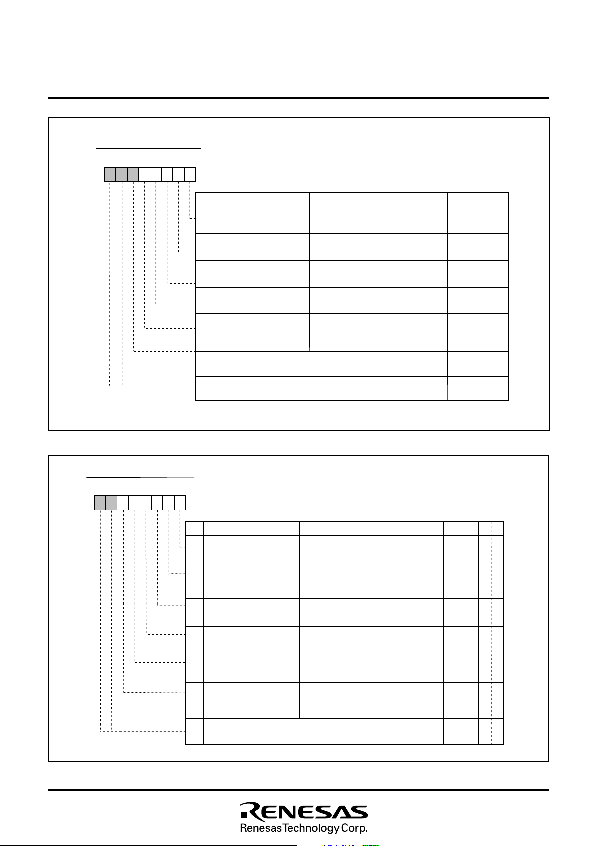
8.4 TIMERS
This microcomputer has 4 timers: timers 1 to 4. All timers are 8-bit
timers with the 8-bit timer latch. The timer block diagram is shown in
Figure 8.4.3.
All of the timers count down and their divide ratio is 1/(n+1), where n
is the value of timer latch. By writing a count value to the corresponding timer latch (addresses 00F016 to 00F316 : timers 1 to 4), the value
is also set to a timer, simultaneously.
The count value is decremented by 1. The timer interrupt request bit
is set to “1” by a timer overflow at the next count pulse, after the
count value reaches “0016.”
8.4.1 Timer 1
Timer 1 can select one of the following count sources:
• f(XIN)/16
• f(XIN)/4096
The count source of timer 1 is selected by setting bit 0 of timer 12
mode register 1 (address 00F416).
Timer interrupt request occurs at timer 1 overflow.
8.4.2 Timer 2
Timer 2 can select one of the following count sources:
• f(XIN)/16
• Timer 1 overflow signal
• External clock from the TIM2 pin
The count source of timer 2 is selected by setting bits 4 and 1 of
timer 12 mode register (address 00F416). When timer 1 overflow
signal is a count source for the timer 2, the timer 1 functions as an 8bit prescaler.
Timer 2 interrupt request occurs at timer 2 overflow.
At reset, timers 3 and 4 are connected by hardware and “FF16” is
automatically set in timer 3; “0716” in timer 4. The f(XIN)/16 is selected as the timer 3 count source. The internal reset is released by
timer 4 overflow in this state and the internal clock is connected.
At execution of the STP instruction, timers 3 and 4 are connected by
hardware and “FF16” is automatically set in timer 3; “0716” in timer 4.
However, the f(XIN)/16 is not selected as the timer 3 count source.
So set both bit 0 of timer 34 mode register (address 00F516) and bit
6 at address 00C716 to “0” before execution of the STP instruction
(f(XIN)/16 is selected as the timer 3 count source). The internal STP
state is released by timer 4 overflow in this state and the internal
clock is connected.
As a result of the above procedure, the program can start under a
stable clock.
The timer-related registers is shown in Figures 8.4.1 and 8.4.2.
8.4.3 Timer 3
Timer 3 can select one of the following count sources:
• f(XIN)/16
• External clock from the HSYNC pin
• External clock from the TIM3 pin
The count source of timer 3 is selected by setting bits 5 and 0 of
timer 34 mode register (address 00F516).
Timer 3 interrupt request occurs at timer 3 overflow.
8.4.4 Timer 4
Timer 4 can select one of the following count sources:
• f(XIN)/16
• f(XIN)/2
• Timer 3 overflow signal
The count source of timer 3 is selected by setting bits 1 and 4 of
timer 34 mode register (address 00F516). When timer 3 overflow
signal is a count source for the timer 4, the timer 3 functions as an 8bit prescaler.
Timer 4 interrupt request occurs at timer 4 overflow.
24
Rev. 1.0
e
2
3
T i m e r 1 2 M o d e R e g i s t e r
234
e
5
b 7b 6 b 5b 4b 3 b 2b 1b 0
0
MITSUBISHI MICROCOMPUTERS
M37212M4/M8–XXXSP, M37212M6–XXXSP/FP
M37212EFSP/FP
SINGLE-CHIP 8-BIT CMOS MICROCOMPUTER for VOLTAGE SYNTHESIZER
with ON-SCREEN DISPLAY CONTROLLER
T i m e r m o d e r e g i s t e r ( T 1 2 M ) [ A d d r e s s 0 0 F 4
1 6
]
Fig. 8.4.1 Timer 12 Mode Register
T i m e r 3 4 M o d e R e g i s t e r
b 7b 6 b 5b 4b 3 b 2b 1b 0
B
0
N a m
T i m e r 1 c o u n t s o u r c e
s e l e c t i o n b i t 1 ( T 1 2 M 0 )
1
T i m e r 2 c o u n t s o u r c e
s e l e c t i o n b i t ( T 1 2 M 1 )
T i m e r 1 c o u n t
s t o p b i t ( T 1 2 M 2 )
T i m e r 2 c o u n t s t o p b i t
( T 1 2 M 3 )
T i m e r 2 i n t e r n a l c o u n t
s o u r c e s e l e c t i o n b i t 2
0 : f ( X
1 : f ( X
0 : I n t e r r u p t c l o c k s o u r c e
1 : E x t e r n a l c l o c k f r o m T I M 2 p i n
0 : C o u n t s t a r t
1 : C o u n t s t o p
0 : C o u n t s t a r t
1 : C o u n t s t o p
0 : f ( X
1 : T i m e r 1 o v e r f l o w
I N
) / 1 6
I N
) / 4 0 9 6
I N
) / 1 6
F u n c t i o n s
( T 1 2 M 4 )
F i x t h i s b i t t o “ 0 . ”
6 , 7N o t h i n g i s a s s i g n e d . T h e s e b i t s a r e w r i t e d i s a b l e b i t s .
W h e n t h e s e b i t s a r e r e a d o u t , t h e v a l u e s a r e “ 0 . ”
1 6
T i m e r 3 4 m o d e r e g i s t e r ( T 3 4 M ) [ A d d r e s s 0 0 F 5
]
A f t e r r e s e t
0
0
0
0
0
0
0—R
R
W
WR
WR
WR
WR
WR
WR
Fig. 8.4.2 Timer 34 Mode Register
Rev. 1.0
B
0
1
N a m
T i m e r 3 c o u n t s o u r c e
s e l e c t i o n b i t ( T 3 4 M 0 )
T i m e r 4 i n t e r n a l
i n t e r r u p t c o u n t s o u r c e
F u n c t i o n s
I N
0 : f ( X
) / 1 6
1 : E x t e r n a l c l o c k s o u r c e
0 : T i m e r 3 o v e r f l o w s i g n a l
1 : f ( X
I N
) / 1 6
s e l e c t i o n b i t ( T 3 4 M 1 )
T i m e r 3 c o u n t s t o p b i t
( T 3 4 M 2 )
T i m e r 4 c o u n t s t o p b i t
( T 3 4 M 3 )
T i m e r 4 c o u n t s o u r c e
4
s e l e c t i o n b i t ( T 3 4 M 4 )
5
T i m e r 3 e x t e r n a l c o u n t
s o u r c e s e l e c t i o n b i t
0 : C o u n t s t a r t
1 : C o u n t s t o p
0 : C o u n t s t a r t
1 : C o u n t s t o p
0 : I n t e r n a l c l o c k s o u r c e
1 : f ( X
I N
) / 2
0 : T I M 3 p i n i n p u t
1 : H
S Y N C
p i n i n p u t
( T 3 4 M 5 )
6 , 7N o t h i n g i s a s s i g n e d . T h e s e b i t s a r e w r i t e d i s a b l e b i t s .
W h e n t h e s e b i t s a r e r e a d o u t , t h e v a l u e s a r e “ 0 . ”
A f t e r r e s e t
RW
0 RW
0RW
0
RW
0
RW
RW
0
RW
0
0—R
25
MITSUBISHI MICROCOMPUTERS
M37212M4/M8–XXXSP, M37212M6–XXXSP/FP
M37212EFSP/FP
SINGLE-CHIP 8-BIT CMOS MICROCOMPUTER for VOLTAGE SYNTHESIZER
with ON-SCREEN DISPLAY CONTROLLER
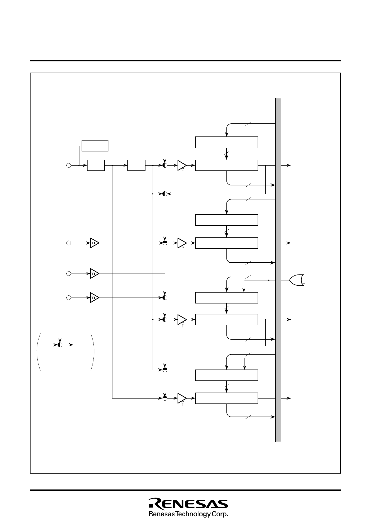
Data bus
8
TIM2
H
TIM3
X
SYNC
1/4096
IN
1/2
1/8
T12M0
T12M4
T12M1
T12M2
T12M3
T34M5
Timer 1 latch (8)
8
Timer 1 (8)
Timer 2 latch (8)
8
Timer 2 (8)
Timer 3 latch (8)
Timer 1
interrupt request
8
8
Timer 2
interrupt request
8
8
FF
16
Reset
STP
instruction
8
Timer 3
interrupt request
T34M0
T34M2
Timer 3 (8)
8
Selection gate :
Connected to black
colored side at reset
T34M1
T12M : Timer 12 mode register
T34M : Timer 34 mode register
T34M4
T34M3
Notes 1: “H” pulse width of external clock inputs TIM2 and TIM3 needs 4 machine cycles or more.
2: When the external clock source is selected, timers 2 and 3 are counted at a rising edge of input signal.
3: In the stop mode or the wait mode, external clock inputs TIM2 and TIM3 cannot be used.
Timer 4 latch (8)
8
Timer 4 (8)
Fig. 8.4.3 Timer Block Diagram
26
8
07
16
Timer 4
interrupt request
8
Rev. 1.0
MITSUBISHI MICROCOMPUTERS
M37212M4/M8–XXXSP, M37212M6–XXXSP/FP
M37212EFSP/FP
SINGLE-CHIP 8-BIT CMOS MICROCOMPUTER for VOLTAGE SYNTHESIZER
with ON-SCREEN DISPLAY CONTROLLER
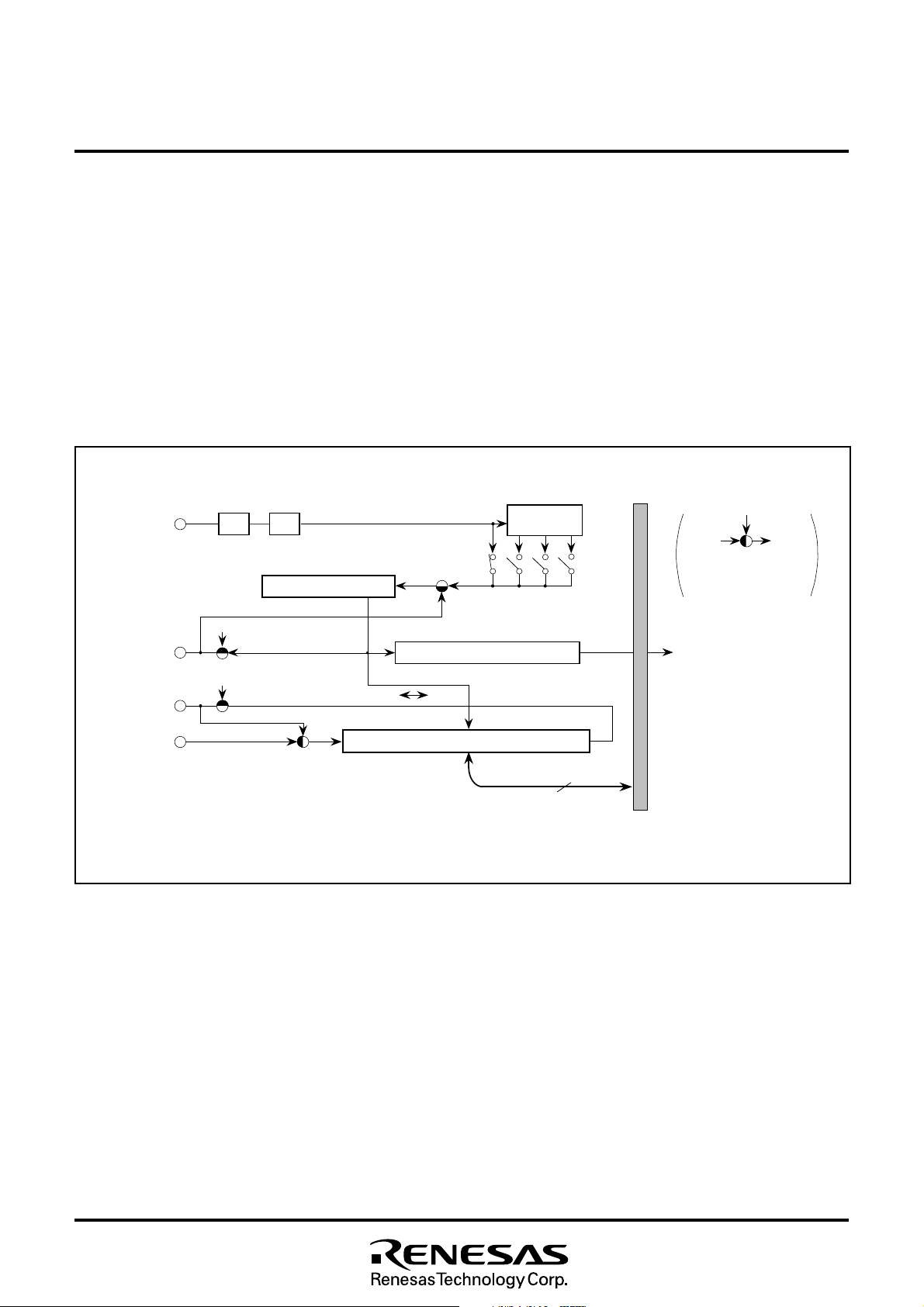
8.5 SERIAL I/O
This microcomputer has a built-in serial I/O which can either transmit
or receive 8-bit data serially in the clock synchronous mode.
The serial I/O block diagram is shown in Figure 8.5.1. The synchronous clock I/O pin (SCLK), data output pin (SOUT), and data input pin
(SIN) also functions as port P4.
Bit 3 of the serial I/O mode register (address 00DC16) selects whether
the synchronous clock is supplied internally or externally (from the
SCLK pin). When an internal clock is selected, bits 1 and 0 select
whether f(XIN) or f(XCIN) is divided by 4, 16, 32, or 64. To use SIN pin
for serial I/O, set the corresponding bit of the port P2 direction register (address 00C516) to “0.”
IN
S
OUT(/IN)
X
S
CLK
S
IN
P4
P4
1/2
1
latch
SM3
0
latch
SM3
1/2
Synchronization circuit
SM5
SM6
SM2
Serial I/O counter (8)
: LSB
MSB
Serial I/O shift register (8)
The operation of the serial I/O is described below. The operation of
the serial I/O differs depending on the clock source; external clock or
internal clock.
Data bus
Frequency
divider
1/81/4 1/16
SM1
S
(See note)
(Address 00DD16)
SM0
8
Selection gate :
Connected to black
colored side at reset.
SM : Serial I/O mode register
Serial I/O interrupt
request
Note : When the data is set in the serial I/O register (address 00DD
Fig. 8.5.1 Serial I/O Block Diagram
Rev. 1.0
16
), the register functions as the serial I/O shift register.
27
MITSUBISHI MICROCOMPUTERS
k
M37212M4/M8–XXXSP, M37212M6–XXXSP/FP
M37212EFSP/FP
SINGLE-CHIP 8-BIT CMOS MICROCOMPUTER for VOLTAGE SYNTHESIZER
with ON-SCREEN DISPLAY CONTROLLER
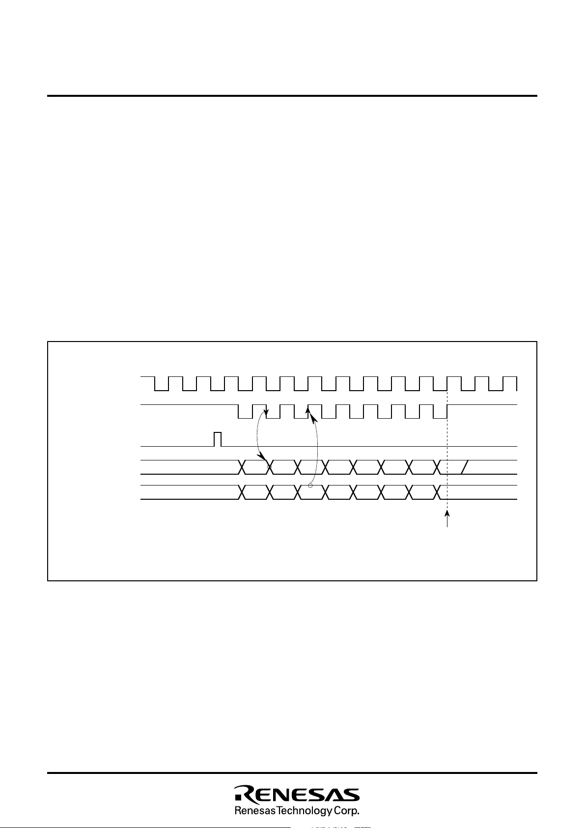
Internal clock : The serial I/O counter is set to “7” during the write
cycle into the serial I/O register (address 00DD16), and the transfer
clock goes HIGH forcibly. At each falling edge of the transfer clock
after the write cycle, serial data is output from the SOUT pin. Transfer
direction can be selected by bit 5 of the serial I/O mode register. At
each rising edge of the transfer clock, data is input from the SIN pin
and data in the serial I/O register is shifted 1 bit.
After the transfer clock has counted 8 times, the serial I/O counter
becomes “0” and the transfer clock stops at HIGH. At this time the
interrupt request bit is set to “1.”
S y n c h r o n o u s c l o c
External clock : The an external clock is selected as the clock source,
the interrupt request is set to “1” after the transfer clock has been
counted 8 counts. However, transfer operation does not stop, so the
clock should be controlled externally. Use the external clock of 1 MHz
or less with a duty cycle of 50%.
The serial I/O timing is shown in Figure 8.5.2. When using an external clock for transfer, the external clock must be held at HIGH for
initializing the serial I/O counter. When switching between an internal clock and an external clock, do not switch during transfer. Also,
be sure to initialize the serial I/O counter after switching.
Notes 1: On programming, note that the serial I/O counter is set by writing to
the serial I/O register with the bit managing instructions, such as SEB
and CLB.
2:When an external clock is used as the synchronous clock, write trans-
mit data to the serial I/O register when the transfer clock input level is
HIGH.
T r a n s f e r c l o c k
S e r i a l I / O r e g i s t e r
w r i t e s i g n a l
S e r i a l I / O o u t p u t
S
O U T
S e r i a l I / O i n p u t
S
I N
N o t e : W h e n a n i n t e r n a l c l o c k i s s e l e c t e d , t h e S
Fig. 8.5.2 Serial I/O Timing (for LSB first)
D
0
D
1
D
2
D
3
D
4
D
O U T
p i n i s a t h i g h - i m p e d a n c e a f t e r t r a n s f e r i s c o m p l e t e d .
( S e e n o t e )
5
D
6
D
7
I n t e r r u p t r e q u e s t b i t i s s e t t o “ 1 ”
28
Rev. 1.0
r
4
W
S e r i a l I / O M o d e R e g i s t e
b 7b 6 b 5b 4b 3 b 2b 1b 0
0
MITSUBISHI MICROCOMPUTERS
M37212M4/M8–XXXSP, M37212M6–XXXSP/FP
M37212EFSP/FP
SINGLE-CHIP 8-BIT CMOS MICROCOMPUTER for VOLTAGE SYNTHESIZER
with ON-SCREEN DISPLAY CONTROLLER
1 6
S e r i a l I / O m o d e r e g i s t e r ( S M ) [ A d d r e s s 0 0 D C
BN
a m
eF
0 , 1I n t e r n a l s y n c h r o n o u s
c l o c k s e l e c t i o n b i t s
( S M 0 , S M 1 )
2
S y n c h r o n o u s c l o c k
s e l e c t i o n b i t ( S M 2 )
b 1 b 0
0 0 : f ( X
0 1 : f ( X
1 0 : f ( X
1 1 : f ( X
0 : E x t e r n a l c l o c k
1 : I n t e r n a l c l o c k
I N
I N
I N
I N
u n c t i o n
) / 4
) / 1 6
) / 3 2
) / 6 4
]
s
A f t e r r e s e t
RW
0RW
0
RW
Fig. 8.5.3 Serial I/O Mode Register
S e r i a l I / O p o r t
3
s e l e c t i o n b i t ( S M 3 )
0 : P 4
1 : S
0
, P 4
O U T ( / I N )
1
, S
C L K
F i x t h i s b i t t o “ 0 . ”
T r a n s f e r d i r e c t i o n
5
s e l e c t i o n b i t ( S M 5 )
S e r i a l i n p u t p i n
6
s e l e c t i o n b i t ( S M 6 )
N o t h i n g i s a s s i g n e d . T h i s b i t i s a w r i t e d i s a b l e b i t .
7
0 : L S B f i r s t
1 : M S B f i r s t
0 : I n p u t s i g n a l f r o m S
1 : I n p u t s i g n a l f r o m S
W h e n t h i s b i t i s r e a d o u t , t h e v a l u e i s “ 0 . ”
I N
O U T
p i n .
p i n .
0
RW
0
R
0
RW
0
RW
0R
—
Rev. 1.0
29

M37212M4/M8–XXXSP, M37212M6–XXXSP/FP
N
SINGLE-CHIP 8-BIT CMOS MICROCOMPUTER for VOLTAGE SYNTHESIZER
8.5.1 Serial I/O Common Transmission/Reception mode
By writing “1” to bit 6 of the serial I/O mode register, signals SIN and
SOUT are switched internally to be able to transmit or receive the
serial data.
Figure 8.5.4 shows signals on serial I/O common transmission/reception mode.
Note: When receiving the serial data after writing “FF16” to the serial I/O regis-
ter.
S
C L K
S
O U T ( / I N )
S
I
MITSUBISHI MICROCOMPUTERS
M37212EFSP/FP
with ON-SCREEN DISPLAY CONTROLLER
C l o c k
“ 1 ”
S e r i a l I / O s h i f t r e g i s t e r ( 8 )
“ 0 ”
S M 6
S M : S e r i a l I / O m o d e r e g i s t e r
Fig. 8.5.4 Signals on Serial I/O Common Transmission/Reception Mode
Rev. 1.0
30

MITSUBISHI MICROCOMPUTERS
M37212M4/M8–XXXSP, M37212M6–XXXSP/FP
M37212EFSP/FP
SINGLE-CHIP 8-BIT CMOS MICROCOMPUTER for VOLTAGE SYNTHESIZER
with ON-SCREEN DISPLAY CONTROLLER
8.6 MULTI-MASTER I2C-BUS INTERFACE
The multi-master I2C-BUS interface is a serial communications circuit, conforming to the Philips I2C-BUS data transfer format. This
interface, offering both arbitration lost detection and a synchronous
functions, is useful for the multi-master serial communications.
Figure 8.6.1 shows a block diagram of the multi-master I2C-BUS interface and Table 8.6.1 shows multi-master I2C-BUS interface functions.
This multi-master I2C-BUS interface consists of the I2C address register, the I2C data shift register, the I2C clock control register, the I2C
control register, the I2C status register and other control circuits.
I2C address register (S0D)
b7 b0
SAD6 SAD5 SAD4 SAD3 SAD2 SAD1 SAD0 RBW
Table 8.6.1 Multi-master I2C-BUS Interface Functions
Item
Function
In conformity with Philips I2C-BUS
standard:
10-bit addressing format
Format
7-bit addressing format
High-speed clock mode
Standard clock mode
In conformity with Philips I2C-BUS
standard:
Master transmission
Communication mode
Master reception
Slave transmission
Slave reception
SCL clock frequency
16.1 kHz to 400 kHz (at φ = 4 MHz)
φ : System clock = f(XIN)/2
Note : We are not responsible for any third party’s infringement of patent rights
or other rights attributable to the use of the control function (bits 6 and 7
2
of the I
C control register at address 00DA16) for connections between
2
the I
C-BUS interface and ports (SCL1, SCL2, SDA1, SDA2).
Interrupt
generating
circuit
Interrupt
request signal
(IICIRQ)
Serial
data
(SDA)
Serial
clock
(SCL)
Noise
elimination
circuit
Noise
elimination
circuit
Data
control
circuit
AL
circuit
BB
circuit
Clock
control
circuit
Address comparator
b7
S0
b7 b0
ACK
I2C clock control register (S2)
2
I C data shift register
FAST
ACK
BIT
CCR4 CCR3 CCR2 CCR1 CCR0
MODE
Clock division
b0
Internal data bus
System clock
b7
MST TRX BB PIN
AL AAS AD0 LRB
2
I C status
(S1)
register
b7 b0
BSEL1 BSEL0
10BIT
ALS
SAD
I2C control register (S1D)
ESO
(φ)
BC2 BC1 BC0
Bit counter
b0
Fig. 8.6.1 Block Diagram of Multi-master I2C-BUS Interface
Rev. 1.0
31

M37212M4/M8–XXXSP, M37212M6–XXXSP/FP
B
f
C
f
C
e
SINGLE-CHIP 8-BIT CMOS MICROCOMPUTER for VOLTAGE SYNTHESIZER
8.6.1 I2C Data Shift Register
The I2C data shift register (S0 : address 00D716) is an 8-bit shift
register to store receive data and write transmit data.
When transmit data is written into this register, it is transferred to the
outside from bit 7 in synchronization with the SCL clock, and each
time one-bit data is output, the data of this register are shifted one bit
to the left. When data is received, it is input to this register from bit 0
in synchronization with the SCL clock, and each time one-bit data is
input, the data of this register are shifted one bit to the left.
The I2C data shift register is in a write enable status only when the
ESO bit of the I2C control register (address 00DA16) is “1.” The bit
counter is reset by a write instruction to the I2C data shift register.
When both the ESO bit and the MST bit of the I2C status register
(address 00D916) are “1,” the SCL is output by a write instruction to
the I2C data shift register. Reading data from the I2C data shift register is always enabled regardless of the ESO bit value.
MITSUBISHI MICROCOMPUTERS
M37212EFSP/FP
with ON-SCREEN DISPLAY CONTROLLER
Note: To write data into the I2C data shift register after setting the MST bit to
“0” (slave mode), keep an interval of 8 machine cycles or more.
D a t a S h i f t R e g i s t e
2
I
b 7b 6b 5b 4b 3b 2b 1b 0
r
2
C d a t a s h i f t r e g i s t e r ( S 0 ) [ A d d r e s s 0 0 D 7
I
N a m
0
D 0 t o D 7
t o
7
d a t a s h i f t r e g i s t e r a f t e r s e t t i n g t h e M S T b i t t
N o t e :
T o w r i t e d a t a i n t o t h e I
“ 0 ” ( s l a v e m o d e ) , k e e p a n i n t e r v a l o f 8 m a c h i n e c y c l e s o r m o r e .
t r e g i s t e r t o s t o r e
T h i s i s a n 8 - b i t s h i
r e c e i v e d a t a a n d w r i t e t r a n s m i t d a t a .
Fig. 8.6.2 Data Shift Register
1 6
]
t e r r e s e
I n d e t e r m i n a t e
F u n c t i o n sA
2
tRW
RW
o
Rev. 1.0
32

M37212M4/M8–XXXSP, M37212M6–XXXSP/FP
/
S
O
B
e
s
W
W
SINGLE-CHIP 8-BIT CMOS MICROCOMPUTER for VOLTAGE SYNTHESIZER
8.6.2 I2C Address Register
The I2C address register (address 00D816) consists of a 7-bit slave
address and a read/write bit. In the addressing mode, the slave address written in this register is compared with the address data to be
received immediately after the START condition are detected.
(1) Bit 0: read/write bit (RBW)
Not used when comparing addresses, in the 7-bit addressing mode.
In the 10-bit addressing mode, the first address data to be received
is compared with the contents (SAD6 to SAD0 + RBW) of the I2C
address register.
The RBW bit is cleared to “0” automatically when the stop condition
is detected.
(2) Bits 1 to 7: slave address (SAD0–SAD6)
These bits store slave addresses. Regardless of the 7-bit addressing mode and the 10-bit addressing mode, the address data transmitted from the master is compared with the contents of these bits.
MITSUBISHI MICROCOMPUTERS
M37212EFSP/FP
with ON-SCREEN DISPLAY CONTROLLER
I2C A d d r e s s R e g i s t e r
b 7b 6b 5b 4b 3b 2b 1b 0
Fig. 8.6.3 I2C Address Register
I2C a d d r e s s r e g i s t e r ( S 0 D ) [ A d d r e s s 0 0 D 8
w r i t e b i
0
R e a d
( R B W )
l a v e a d d r e s
1
( S A D 0 t o S A D 6 )
t o
7
N a m
t
s
n l y i n 1 0 - b i t a d d r e s s i n g ( i n s l a v e ) m o d e
<
T h e l a s t s i g n i f i c a n t b i t o f a d d r e s s d a t a i s
c o m p a r e d .
0 : W a i t t h e f i r s t b y t e o f s l a v e a d d r e s s a f t e r
S T A R T c o n d i t i o n
1 : W a i t t h e f i r s t b y t e o f s l a v e a d d r e s s a f t e r
R E S T A R T c o n d i t i o n
< I n b o t h m o d e s >
T h e a d d r e s s d a t a i s c o m p a r e d .
F u n c t i o n
1 6
]
A f t e r r e s e t
>
( r e a d s t a t e )
( w r i t e s t a t e )
R
0
R—
0
R
Rev. 1.0
33

MITSUBISHI MICROCOMPUTERS
r
S C
S C
S
S
B
e
s
W
C
C
C
C
S
S
S
S
)
(
)
S
f
W
WRW
W
M37212M4/M8–XXXSP, M37212M6–XXXSP/FP
M37212EFSP/FP
SINGLE-CHIP 8-BIT CMOS MICROCOMPUTER for VOLTAGE SYNTHESIZER
with ON-SCREEN DISPLAY CONTROLLER
8.6.3 I2C Clock Control Register
The I2C clock control register (address 00DB16) is used to set ACK
control, SCL mode and SCL frequency.
(4) Bit 7: ACK clock bit (ACK)
This bit specifies a mode of acknowledgment which is an acknowledgment response of data transmission. When this bit is set to “0,”
the no ACK clock mode is set. In this case, no ACK clock occurs
(1) Bits 0 to 4: SCL frequency control bits (CCR0–CCR4)
These bits control the SCL frequency.
after data transmission. When the bit is set to “1,” the ACK clock
mode is set and the master generates an ACK clock upon completion of each 1-byte data transmission.The device for transmitting
(2) Bit 5: SCL mode specification bit (FAST MODE)
This bit specifies the SCL mode. When this bit is set to “0,” the standard clock mode is set. When the bit is set to “1,” the high-speed
address data and control data releases the SDA at the occurrence of
an ACK clock (make SDA HIGH) and receives the ACK bit generated
by the data receiving device.
clock mode is set.
Note: Do not write data into the I2C clock control register during transmission.
(3) Bit 6: ACK bit (ACK BIT)
This bit sets the SDA status when an ACK clock✽ is generated. When
this bit is set to “0,” the ACK return mode is set and SDA goes to
LOW at the occurrence of an ACK clock. When the bit is set to “1,”
the ACK non-return mode is set. The SDA is held in the HIGH status
at the occurrence of an ACK clock.
However, when the slave address matches the address data in the
reception of address data at ACK BIT = “0,” the SDA is automatically
made LOW (ACK is returned). If there is a mismatch between the
slave address and the address data, the SDA is automatically made
HIGH (ACK is not returned).
✽ACK clock: Clock for acknowledgement
If data is written during transmission, the I
that data cannot be transmitted normally.
2
C clock generator is reset, so
I2C C l o c k C o n t r o l R e g i s t e
b 7b 6b 5b 4b 3b 2b 1b 0
2
I
C c l o c k c o n t r o l r e g i s t e r ( S 2 ) [ A d d r e s s 0 0 D B
L f r e q u e n c y c o n t r o l b i t
0
( C C R 0 t o C C R 4 )
t o
4
L m o d
5
s p e c i f i c a t i o n b i t
( F A S T M O D E )
K b i
A
6
( A C K B I T )
K c l o c k b i
A
7
( A C K )
N o t e : A t 4 0 0 k H z i n t h e h i g h - s p e e d c l o c k m o d e , t h e d u t y i s a s b e l o w .
“ 0 ” p e r i o d : “ 1 ” p e r i o d = 3 : 2
I n t h e o t h e r c a s e s , t h e d u t y i s a s b e l o w .
“ 0 ” p e r i o d : “ 1 ” p e r i o d = 1 : 1
1 6
]
N a m
e t u p v a l u e o
C R 4 – C C R
s
C
0 0 t o 0 2
0 5
.
.
1 D
1 E
1 F
t a n d a r d c l o c k m o d
e
t
t
0 :
1 : H i g h - s p e e d c l o c k m o d e
K i s r e t u r n e d
0 : A
1 : A C K i s n o t r e t u r n e d .
K c l o c
0 : N o A
1 : A C K c l o c k
F u n c t i o n
t a n d a r d c l o c
o d
0
m
e t u p d i s a b l e
e t u p d i s a b l e
e t u p d i s a b l e
1 0 0
8 3 . 31
.
5 0 0 / C C R v a l u e
1 7 . 2 3 4 . 5
1 6 . 63
1 6 . 1
a t
= 4 M H z , u n i t : k H z
φ
.
k
k
e
e t u p d i s a b l e
d
d
d
( S e e n o t e
1 0 0 0 / C C R v a l u e
e
H i g h s p e e d
c l o c k m o d e
3 3 30 3
2 5 00 4
4 0 0
6
60 6
3 .
3
3 2 . 3
A f t e r r e s e t
d
R
0
R
0
R
0
0
R
Fig. 8.6.4 I2C Address Register
Rev. 1.0
34

MITSUBISHI MICROCOMPUTERS
M37212M4/M8–XXXSP, M37212M6–XXXSP/FP
M37212EFSP/FP
SINGLE-CHIP 8-BIT CMOS MICROCOMPUTER for VOLTAGE SYNTHESIZER
with ON-SCREEN DISPLAY CONTROLLER
8.6.4 I2C Control Register
The I2C control register (address 00DA16) controls the data communication format.
(1) Bits 0 to 2: bit counter (BC0–BC2)
These bits decide the number of bits for the next 1-byte data to be
transmitted. An interrupt request signal occurs immediately after the
number of bits specified with these bits are transmitted.
When a START condition is received, these bits become “0002” and
the address data is always transmitted and received in 8 bits.
(2) Bit 3: I2C interface use enable bit (ESO)
This bit enables usage of the multimaster I2C BUS interface. When
this bit is set to “0,” the use disable status is provided, so the SDA
and the SCL become high-impedance. When the bit is set to “1,” use
of the interface is enabled.
When ESO = “0,” the following is performed.
• PIN = “1,” BB = “0” and AL = “0” are set (they are bits of the I2C
status register at address 00D916 ).
• Writing data to the I2C data shift register (address 00D716) is dis-
abled.
S C L
M u l t i - m a s t e r
I2C - B U S
i n t e r f a c e
S D A
(3) Bit 4: data format selection bit (ALS)
This bit decides whether or not to recognize slave addresses. When
this bit is set to “0,” the addressing format is selected, so that address data is recognized. When a match is found between a slave
address and address data as a result of comparison or when a general call (refer to “8.6.5 I2C Status Register,” bit 1) is received, transmission processing can be performed. When this bit is set to “1,” the
free data format is selected, so that slave addresses are not recognized.
(4) Bit 5: addressing format selection bit (10BIT SAD)
This bit selects a slave address specification format. When this bit is
set to “0,” the 7-bit addressing format is selected. In this case, only
the high-order 7 bits (slave address) of the I2C address register (address 00D816) are compared with address data. When this bit is set
to “1,” the 10-bit addressing format is selected, all the bits of the I2C
address register are compared with address data.
(5) Bits 6 and 7: connection control bits between
2
C-BUS interface and ports
I
(BSEL0, BSEL1)
These bits controls the connection between SCL and ports or SDA
and ports (refer to Figure 8.6.5).
“ 0 ”
“ 1 ” B S E L 0
“ 0 ”
S C L 1 / P 1
“ 1 ” B S E L 1
S C L 2 / P 1
“ 0 ”
“ 1 ” B S E L 0
S D A 1 / P 1
“ 0 ”
“ 1 ” B S E L 1
S D A 2 / P 1
1
2
3
4
Note: Set the corresponding direction register to “1” to use the
port as multi-master I2C-BUS interface.
Fig. 8.6.5 Connection Port Control by BSEL0 and BSEL1
Rev. 1.0
35

f
f
7
C
C
)
I2C C o n t r o l R e g i s t e r
B
e
s
W
WRWRWRWRW
MITSUBISHI MICROCOMPUTERS
M37212M4/M8–XXXSP, M37212M6–XXXSP/FP
M37212EFSP/FP
SINGLE-CHIP 8-BIT CMOS MICROCOMPUTER for VOLTAGE SYNTHESIZER
with ON-SCREEN DISPLAY CONTROLLER
b 7b 6b 5b 4b 3b 2b 1b 0
2
C c o n t r o l r e g i s t e r ( S 1 D ) [ A d d r e s s 0 0 D A1
I
N a m
0
B i t c o u n t e r
t o
( N u m b e r o f t r a n s m i t / r e c i e v e
2
b i t s )
( B C 0 t o B C 2 )
2
3
C - B U S i n t e r f a c e u s e
I
e n a b l e b i t ( E S O )
o r m a t s e l e c t i o n
4D a t a
b i t ( A L S )
o r m a t s e l e c t i o n
5A d d r e s s i n g
b i t ( 1 0 B I T S A D )
o n n e c t i o n c o n t r o l b i t s
6 ,
2
b e t w e e n I C - B U S i n t e r f a c e
a n d p o r t s
( B S E L 0 , B S E L 1 )
6]
F u n c t i o n
b 2 b 1 b 0
0 0 0 : 8
0 0 1 : 7
0 1 0 : 6
0 1 1 : 5
1 0 0 : 4
1 0 1 : 3
1 1 0 : 2
1 1 1 : 1
0 : D i s a b l e d
1 : E n a b l e d
f o r m a
0 : A d d r e s s i n g
1 : F r e e d a t a f o r m a t
f o r m a
0 : 7 - b i t a d d r e s s i n g
1 : 1 0 - b i t a d d r e s s i n g f o r m a t
o n n e c t i o n p o r t ( S e e n o t e
b 7 b 6
0 0 : N o n e
0 1 : S C L 1 , S D A 1
1 0 : S C L 2 , S D A 2
1 1 : S C L 1 , S D A 1 , S C L 2 , S D A 2
t
t
A f t e r r e s e t
0
0
0
0
0
R
R
Fig. 8.6.6 I2C Control Register
Rev. 1.0
36

MITSUBISHI MICROCOMPUTERS
M37212M4/M8–XXXSP, M37212M6–XXXSP/FP
M37212EFSP/FP
SINGLE-CHIP 8-BIT CMOS MICROCOMPUTER for VOLTAGE SYNTHESIZER
with ON-SCREEN DISPLAY CONTROLLER
8.6.5 I2C Status Register
The I2C status register (address 00D916) controls the I2C-BUS interface status. The low-order 4 bits are read-only bits and the highorder 4 bits can be read out and written to.
(1) Bit 0: last receive bit (LRB)
This bit stores the last bit value of received data and can also be
used for ACK receive confirmation. If ACK is returned when an ACK
clock occurs, the LRB bit is set to “0.” If ACK is not returned, this bit is
set to “1.” Except in the ACK mode, the last bit value of received data
is input. The state of this bit is changed from “1” to “0” by executing a
write instruction to the I2C data shift register (address 00D716).
(2) Bit 1: general call detecting flag (AD0)
This bit is set to “1” when a general call✽ whose address data is all
“0” is received in the slave mode. By a general call of the master
device, every slave device receives control data after the general
call. The AD0 bit is set to “0” by detecting the STOP condition or
START condition.
✽General call: The master transmits the general call address “0016”
to all slaves.
(3) Bit 2: slave address comparison flag (AAS)
This flag indicates a comparison result of address data.
■ In the slave receive mode, when the 7-bit addressing format is
selected, this bit is set to “1” in one of the following conditions.
• The address data immediately after occurrence of a START con-
dition matches the slave address stored in the high-order 7 bits
of the I2C address register (address 00D816).
• A general call is received.
■ In the slave reception mode, when the 10-bit addressing format is
selected, this bit is set to “1” with the following condition.
• When the address data is compared with the I2C address regis-
ter (8 bits consists of slave address and RBW), the first bytes
match.
■ The state of this bit is changed from “1” to “0” by executing a write
instruction to the I2C data shift register (address 00D716).
(4) Bit 3: arbitration lost✽ detecting flag (AL)
n the master transmission mode, when a device other than the microcomputer sets the SDA to “L,”, arbitration is judged to have been
lost, so that this bit is set to “1.” At the same time, the TRX bit is set to
“0,” so that immediately after transmission of the byte whose arbitration was lost is completed, the MST bit is set to “0.” When arbitration
is lost during slave address transmission, the TRX bit is set to “0” and
the reception mode is set. Consequently, it becomes possible to receive and recognize its own slave address transmitted by another
master device.
✽Arbitration lost: The status in which communication as a master is
disabled.
(5) Bit 4: I2C-BUS interface interrupt request bit (PIN)
This bit generates an interrupt request signal. Each time 1-byte data
is transmitted, the state of the PIN bit changes from “1” to “0.” At the
same time, an interrupt request signal is sent to the CPU. The PIN bit
is set to “0” in synchronization with a falling edge of the last clock
(including the ACK clock) of an internal clock and an interrupt request signal occurs in synchronization with a falling edge of the PIN
bit. When the PIN bit is “0,” the SCL is kept in the “0” state and clock
generation is disabled. Figure 8.6.8 shows an interrupt request signal generating timing chart.
The PIN bit is set to “1” in any one of the following conditions.
• Executing a write instruction to the I2C data shift register (address
00D716).
• When the ESO bit is “0”
• At reset
The conditions in which the PIN bit is set to “0” are shown below:
• Immediately after completion of 1-byte data transmission (including when arbitration lost is detected)
• Immediately after completion of 1-byte data reception
• In the slave reception mode, with ALS = “0” and immediately after
completion of slave address or general call address reception
• In the slave reception mode, with ALS = “1” and immediately after
completion of address data reception
(6) Bit 5: bus busy flag (BB)
This bit indicates the status of use of the bus system. When this bit is
set to “0,” this bus system is not busy and a STAR T condition can be
generated. When this bit is set to “1,” this bus system is busy and the
occurrence of a STAR T condition is disabled by the START condition
duplication prevention function (See note).
This flag can be written by software only in the master transmission
mode. In the other modes, this bit is set to “1” by detecting a START
condition and set to “0” by detecting a STOP condition. When the
ESO bit of the I2C control register (address 00DA16) is “0” and at
reset, the BB flag is kept in the “0” state.
(7) Bit 6: communication mode specification bit
(transfer direction specification bit: TRX)
This bit decides the direction of transfer for data communication. When
this bit is “0,” the reception mode is selected and the data of a transmitting device is received. When the bit is “1,” the transmission mode
is selected and address data and control data are output into the
SDA in synchronization with the clock generated on the SCL.
When the ALS bit of the I2C control register (address 00DA16) is “0”
in the slave reception mode is selected, the TRX bit is set to “1”
(transmit) if the least significant bit (R/W bit) of the address data transmitted by the master is “1.” When the ALS bit is “0” and the R/W bit is
“0,” the TRX bit is cleared to “0” (receive).
The TRX bit is cleared to “0” in one of the following conditions.
• When arbitration lost is detected.
• When a STOP condition is detected.
• When occurence of a START condition is disabled by the START
condition duplication prevention function (Note).
• With MST = “0” and when a START condition is detected.
• With MST = “0” and when ACK non-return is detected.
• At reset
___
___
Rev. 1.0
37

MITSUBISHI MICROCOMPUTERS
7
B
e
s
W
C
f
)
f
S
G
“
)
W
W
( S
)
( S
)
( S
)
( S
)
Q
M37212M4/M8–XXXSP, M37212M6–XXXSP/FP
M37212EFSP/FP
SINGLE-CHIP 8-BIT CMOS MICROCOMPUTER for VOLTAGE SYNTHESIZER
with ON-SCREEN DISPLAY CONTROLLER
(8) Bit 7: Communication mode specification bit
(master/slave specification bit: MST)
This bit is used for master/slave specification for data communication. When this bit is “0,” the slave is specified, so that a START
condition and a STOP condition generated by the master are received,
and data communication is performed in synchronization with the
clock generated by the master. When this bit is “1,” the master is
specified and a START condition and a STOP condition are generated, and also the clocks required for data communication are generated on the SCL.
The MST bit is cleared to “0” in one of the following conditions.
• Immediately after completion of 1-byte data transmission when
arbitration lost is detected
• When a STOP condition is detected.
• When occurence of a START condition is disabled by the START
condition duplication preventing function (Note).
• At reset
I2C S t a t u s R e g i s t e r
b 7b 6b 5b 4b 3b 2b 1b 0
I2C s t a t u s r e g i s t e r ( S 1 ) [ A d d r e s s 0 0 D 9
N a m
( L R B
0
L a s t r e c e i v e b i t
( S e e n o t e )
e n e r a l c a l l d e t e c t i n g f l a g
1
( A D 0 ) ( S e e n o t e )
l a v e a d d r e s s c o m p a r i s o n
2
f l a g ( A A S ) ( S e e n o t e )
l a g
3
A r b i t r a t i o n l o s t d e t e c t i n g
( A L ) ( S e e n o t e )
2
4
C - B U S i n t e r f a c e i n t e r r u p t
I
r e q u e s t b i t ( P I N )
f l a g ( B B
5
B u s b u s y
o m m u n i c a t i o n m o d e
6 ,
s p e c i f i c a t i o n b i t s
( T R X , M S T )
f l a g s c a n b e r e a d o u t , b u t c a n n n o t b e w r i t t e n
N o t e : T h e s e b i t s a n d
Note:The START condition duplication prevention function disables the ST AR T
condition generation, reset of bit counter reset, and SCL output, when
the following condition is satisfied:
a START condition is set by another master device.
1 6
]
0
0 : L a s t b i t =
1 : L a s t b i t = “ 1 ”
0 : N o g e n e r a l c a l l d e t e c t e d
1 : G e n e r a l c a l l d e t e c t e d
0 : A d d r e s s m i s m a t c h
1 : A d d r e s s m a t c h
0 : N o t d e t e c t e d
1 : D e t e c t e d
0 : I n t e r r u p t r e q u e s t i s s u e d
1 : N o i n t e r r u p t r e q u e s t i s s u e d
r e
0 : B u s
1 : B u s b u s y
b 7 b 6
0 0 : S l a v e r e c i e v e m o d e
0 1 : S l a v e t r a n s m i t m o d e
1 0 : M a s t e r r e c i e v e m o d e
1 1 : M a s t e r t r a n s m i t m o d e
F u n c t i o n
”
e
e e n o t e
e e n o t e
e e n o t e
e e n o t e
.
A f t e r r e s e t
I n d e t e r m i n a t e
0
0
0
1
0
0
R
R—
R—
R—
R—
RW
R
R
Fig. 8.6.7 I2C Status Register
S C L
P I N
I I C I R
Fig. 8.6.8 Interrupt Request Signal Generation Timing
Rev. 1.0
38

MITSUBISHI MICROCOMPUTERS
M37212M4/M8–XXXSP, M37212M6–XXXSP/FP
M37212EFSP/FP
SINGLE-CHIP 8-BIT CMOS MICROCOMPUTER for VOLTAGE SYNTHESIZER
with ON-SCREEN DISPLAY CONTROLLER
8.6.6 START Condition Generation Method
When the ESO bit of the I2C control register (address 00DA16) is “1,”
execute a write instruction to the I2C status register (address 00D916)
to set the MST, TRX and BB bits to “1.” A START condition will then
be generated. After that, the bit counter becomes “0002” and an SCL
for 1 byte is output. The START condition generation timing and BB
bit set timing are different in the standard clock mode and the highspeed clock mode. Refer to Figure 8.6.9 for the START condition
generation timing diagram, and Table 8.6.2 for the START condition/
STOP condition generation timing table.
8.6.7 STOP Condition Generation Method
When the ESO bit of the I2C control register (address 00DA16) is “1,”
execute a write instruction to the I2C status register (address 00D916)
for setting the MST bit and the TRX bit to “1” and the BB bit to “0”. A
STOP condition will then be generated. The STOP condition generation timing and the BB flag reset timing are different in the standard
clock mode and the high-speed clock mode. Refer to Figure 8.6.10
for the STOP condition generation timing diagram, and Table 8.6.2
for the START condition/STOP condition generation timing table.
I2C status register
write signal
SCL
SDA
BB flag
Fig. 8.6.9 START Condition Generation Timing Diagram
I2C s t a t u s r e g i s t e r
w r i t e s i g n a l
S C L
S D A
B B f l a g
Setup
time
Setup
time
S e t u p
t i m e
Hold time
Set time for
BB flag
H o l d t i m e
R e s e t t i m e f o r
B B f l a g
Fig. 8.6.10 STOP Condition Generation Timing Diagram
Table 8.6.2 START Condition/STOP Condition Generation Tim-
ing Table
Item
Setup time
(START condition)
Setup time
(STOP condition)
Hold time
Set/reset time
for BB flag
Note: Absolute time at φ = 4 MHz. The value in parentheses denotes the
number of φ cycles.
Standard Clock Mode
5.0 µs (20 cycles)
4.25 µs (17 cycles)
5.0 µs (20 cycles)
3.0 µs (12 cycles)
High-speed Clock Mode
2.5 µs (10 cycles)
1.75 µs (7 cycles)
2.5 µs (10 cycles)
1.5 µs (6 cycles)
Rev. 1.0
39

MITSUBISHI MICROCOMPUTERS
M37212M4/M8–XXXSP, M37212M6–XXXSP/FP
M37212EFSP/FP
SINGLE-CHIP 8-BIT CMOS MICROCOMPUTER for VOLTAGE SYNTHESIZER
with ON-SCREEN DISPLAY CONTROLLER
8.6.8 ST ART/STOP Condition Detect Conditions
The START/STOP condition detect conditions are shown in
Figure 8.6.11 and Table 8.6.3. Only when the 3 conditions of Table
8.6.3 are satisfied, a START/STOP condition can be detected.
Note: When a STOP condition is detected in the slave mode
(MST = 0), an interrupt request signal “IICIRQ” is generated to the
CPU.
S C L r e l e a s e t i m e
S C L
S D A
( S T A R T c o n d i t i o n )
S D A
( S T O P c o n d i t i o n )
Fig. 8.6.11 START Condition/STOP Condition Detect Timing Dia-
gram
Table 8.6.3 START Condition/STOP Condition Detect Conditions
Standard Clock Mode
6.5 µs (26 cycles) < SCL
3.25 µs (13 cycles) < Setup time
3.25 µs (13 cycles) < Hold time
Note:Absolute time at φ = 4 MHz. The value in parentheses denotes the num-
ber of φ cycles.
release time
S e t u p
t i m e
S e t u p
t i m e
H o l d t i m e
H o l d t i m e
High-speed Clock Mode
1.0 µs (4 cycles) < SCL
0.5 µs (2 cycles) < Setup time
0.5 µs (2 cycles) < Hold time
release time
8.6.9 Address Data Communication
There are two address data communication formats, namely, 7-bit
addressing format and 10-bit addressing format. The respective address communication formats is described below.
(1) 7-bit addressing format
To meet the 7-bit addressing format, set the 10BIT SAD bit of the I2C
control register (address 00DA16) to “0.” The first 7-bit address data
transmitted from the master is compared with the high-order 7-bit
slave address stored in the I2C address register (address 00D816).
At the time of this comparison, address comparison of the RBW bit of
the I2C address register (address 00D816) is not made. For the data
transmission format when the 7-bit addressing format is selected,
refer to Figure 8.6.12, (1) and (2).
(2) 10-bit addressing format
To meet the 10-bit addressing format, set the 10BIT SAD bit of the
I2C control register (address 00DA16) to “1.” An address comparison
is made between the first-byte address data transmitted from the
master and the 7-bit slave address stored in the I2C address register
(address 00D816). At the time of this comparison, an address comparison between the RBW bit of the I2C address register (address
00D816) and the R/W bit which is the last bit of the address data
transmitted from the master is made. In the 10-bit addressing mode,
the R/W bit which is the last bit of the address data not only specifies
the direction of communication for control data but also is processed
as an address data bit.
When the first-byte address data matches the slave address, the
AAS bit of the I2C status register (address 00D916) is set to “1.” After
the second-byte address data is stored into the I2C data shift register
(address 00D716), make an address comparison between the second-byte data and the slave address by software. When the address
data of the 2nd bytes matches the slave address, set the RBW bit of
the I2C address register (address 00D816) to “1” by software. This
processing can match the 7-bit slave address and R/W data, which
are received after a RESTART condition is detected, with the value
of the I2C address register (address 00D816). For the data transmission format when the 10-bit addressing format is selected, refer to
Figure 8.6.12, (3) and (4).
40
Rev. 1.0

MITSUBISHI MICROCOMPUTERS
M37212M4/M8–XXXSP, M37212M6–XXXSP/FP
M37212EFSP/FP
SINGLE-CHIP 8-BIT CMOS MICROCOMPUTER for VOLTAGE SYNTHESIZER
with ON-SCREEN DISPLAY CONTROLLER
8.6.10 Example of Master Transmission
An example of master transmission in the standard clock mode, at
the SCL frequency of 100 kHz and in the ACK return mode is shown
below.
➀ Set a slave address in the high-order 7 bits of the I2C address
register (address 00D816) and “0” in the RBW bit.
➁ Set the ACK return mode and SCL = 100 kHz by setting “8516” in
the I2C clock control register (address 00DB16).
➂ Set “1016” in the I2C status register (address 00D916) and hold the
SCL at the HIGH.
④ Set a communication enable status by setting “4816” in the I2C
control register (address 00DA16).
➄ Set the address data of the destination of transmission in the high-
order 7 bits of the I2C data shift register (address 00D716) and set
“0” in the least significant bit.
⑥ Set “F016” in the I2C status register (address 00D916) to generate
a START condition. At this time, an SCL for 1 byte and an ACK
clock automatically occurs.
⑦ Set transmit data in the I2C data shift register (address 00D716). At
this time, an SCL and an ACK clock automatically occurs.
➇ When transmitting control data of more than 1 byte, repeat step ➆.
➈ Set “D016” in the I2C status register (address 00D916). After this, if
ACK is not returned or transmission ends, a STOP condition will
be generated.
8.6.11 Example of Slave Reception
An example of slave reception in the high-speed clock mode, at the
SCL frequency of 400 kHz, in the ACK non-return mode, using the
addressing format, is shown below.
➀ Set a slave address in the high-order 7 bits of the I2C address
register (address 00D816) and “0” in the RBW bit.
➁ Set the no ACK clock mode and SCL = 400 kHz by setting “2516” in
the I2C clock control register (address 00DB16).
➂ Set “1016” in the I2C status register (address 00D916) and hold the
SCL at the HIGH.
④ Set a communication enable status by setting “4816” in the I2C
control register (address 00DA16).
➄ When a START condition is received, an address comparison is
made.
⑥ •When all transmitted address are“0” (general call):
AD0 of the I2C status register (address 00D916) is set to “1”and
an interrupt request signal occurs.
•When the transmitted addresses match the address set in ➀:
ASS of the I2C status register (address 00D916) is set to “1” and
an interrupt request signal occurs.
•In the cases other than the above:
AD0 and AAS of the I2C status register (address 00D916) are set
to “0” and no interrupt request signal occurs.
⑦ Set dummy data in the I2C data shift register (address 00D716).
➇ When receiving control data of more than 1 byte, repeat step ➆.
➈ When a STOP condition is detected, the communication ends.
Rev. 1.0
41

MITSUBISHI MICROCOMPUTERS
A
A
A
A
r
A
A
A
s
A
A
M37212M4/M8–XXXSP, M37212M6–XXXSP/FP
M37212EFSP/FP
SINGLE-CHIP 8-BIT CMOS MICROCOMPUTER for VOLTAGE SYNTHESIZER
with ON-SCREEN DISPLAY CONTROLLER
SS l a v e a d d r e s s
( 1 ) A m a s t e r - t r a n s m i t t e r t r a n s m i t s d a t a t o a s l a v e - r e c e i v e r
( 2 ) A m a s t e r - r e c e i v e r r e c e i v e s d a t a f r o m a s l a v e - t r a n s m i t t e
( 3 ) A m a s t e r - t r a n s m i t t e r t r a n s m i t s d a t a t o a s l a v e - r e c e i v e r w i t h a 1 0 - b i t a d d r e s s
: S T O P c o n d i t i o
/ W : R e a d / W r i t e b i
( 4 ) A m a s t e r - r e c e i v e r r e c e i v e s d a t a f r o m a s l a v e - t r a n s m i t t e r w i t h a 1 0 - b i t a d d r e s s
S:S T A R T c o n d i t i o nP
A:A C K b i tR
S r:R e s t a r t c o n d i t i o n
7 b i t s“
SS l a v e a d d r e s s
7 b i t s“
S l a v e a d d r e s s
S
1 s t 7 b i t s
7 b i t s“
S l a v e a d d r e s s
S
1 s t 7 b i t s
7 b i t s“
0
”1
R / W
1
”1
R / W
0
”8
R / W R / W
0
”8
D a t aAD a t aA / A PR / W
t o 8 b i t
s1 t o 8 b i t s
D a t a AD a t a AP
t o 8 b i t
s1 t o 8 b i t s
S l a v e a d d r e s s
2 n d b y t e
b i t
s1
S l a v e a d d r e s s
2 n d b y t e
b i t
s7
n
t
Fig. 8.6.12 Address Data Communication Format
8.6.12 Precautions when using multi-master
2
C-BUS interface
I
(1) Read-modify-write instruction
The precautions when the raead-modify-write instruction such as SEB,
CLB etc. is executed for each register of the multi-master I2C-BUS
interface are described below.
•I2C data shift register (S0)
When executing the read-modify-write instruction for this register
during transfer, data may become a value not intended.
•I2C address register (S0D)
When the read-modify-write instruction is executed for this register
at detecting the STOP condition, data may become a value not
intended. It is because hardware changes the read/write bit (RBW)
at the above timing.
•I2C status register (S1)
Do not execute the read-modify-write instruction for this register
because all bits of this register are changed by hardware.
•I2C control register (S1D)
When the read-modify-write instruction is executed for this register
at detecting the STAR T condition or at completing the byte transfer ,
data may become a value not intended. Because hardware changes
the bit counter (BC0–BC2) at the above timing.
•I2C clock control register (S2)
The read-modify-write instruction can be executed for this register.
______
D a t a
t o 8 b i t
S l a v e a d d r e s s
S r
1 s t 7 b i t s
F r o m m a s t e r t o s l a v e
F r o m s l a v e t o m a s t e r
s
b i t
D a t aA / A P
1 t o 8 b i t s
1 t o 8 b i t s
D a t a
D a t a
1 t o 8 b i t s“ 1 ”
P
(2) START condition generating procedure us-
ing multi-master
➀Procedure example (The necessary conditions of the generating
procedure are described as the following ➁ to ➄).
•
•
LDA — (Taking out of slave address value)
SEI (Interrupt disabled)
BBS 5,S1,BUSBUSY
BUSFREE:
STA S0 (Writing of slave address value)
LDM #$F0, S1
CLI (Interrupt enabled)
•
•
BUSBUSY:
CLI (Interrupt enabled)
•
•
➁Use “STA,” “STX” or “STY” of the zero page addressing instruction
for writing the slave address value to the I2C data shift register.
➂Use “LDM” instruction for setting trigger of START condition gener-
ating.
④Write the slave address value of above ➁ and set trigger of START
condition generating of above ➂ continuously shown the above
procedure example.
➄Disable interrupts during the following three process steps:
• BB flag confirming
• Writing of slave address value
• Trigger of START condition generating
When the condition of the BB flag is bus busy, enable interrupts
immediately.
(BB flag confirming and branch process)
(Trigger of ST ART condition generating)
Rev. 1.0
42

MITSUBISHI MICROCOMPUTERS
M37212M4/M8–XXXSP, M37212M6–XXXSP/FP
M37212EFSP/FP
SINGLE-CHIP 8-BIT CMOS MICROCOMPUTER for VOLTAGE SYNTHESIZER
with ON-SCREEN DISPLAY CONTROLLER
(3) RESTART condition generating procedure
➀Procedure example (The necessary conditions of the generating
procedure are described as the following ➁ to ➅.)
Execute the following procedure when the PIN bit is “0.”
•
•
LDM #$00, S1 (Select slave receive mode)
LDA — (Taking out of slave address value)
SEI (Interrupt disabled)
STA S0 (Writing of slave address value)
LDM #$F0, S1 (Trigger of RESTART condition generating)
CLI (Interrupt enabled)
•
•
➁Select the slave receive mode when the PIN bit is “0.” Do not write
“1” to the PIN bit. Neither “0” nor “1” is specified for the writing to
the BB bit.
The TRX bit becomes “0” and the SDA pin is released.
➂The SCL pin is released by writing the slave address value to the
I2C data shift register. Use “STA,” “STX” or “STY” of the zero page
addressing instruction for writing.
④Use “LDM” instruction for setting trigger of RESTAR T condition gen-
erating.
➄Write the slave address value of above ➂ and set trigger of RE-
START condition generating of above ➃ continuously shown the
above procedure example.
⑥Disable interrupts during the following two process steps:
• Writing of slave address value
• Trigger of RESTART condition generating
(4) STOP condition generating procedure
➀Procedure example (The necessary conditions of the generating
procedure are described as the following ➁ to ➃.)
•
•
SEI (Interrupt disabled)
LDM #$C0, S1 (Select master transmit mode)
NOP (Set NOP)
LDM #$D0, S1 (Trigger of STOP condition generating)
CLI (Interrupt enabled)
•
•
➁Write “0” to the PIN bit when master transmit mode is select.
➂Execute “NOP” instruction after setting of master transmit mode.
Also, set trigger of STOP condition generating within 10 cycles after selecting of master trasmit mode.
④Disable interrupts during the following two process steps:
• Select of master transmit mode
• Trigger of STOP condition generating
(5) Writing to I2C status register
Do not execute an instruction to set the PIN bit to “1” from “0” and an
instruction to set the MST and TRX bits to “0” from “1” simultaneously .
It is because it may enter the state that the SCL pin is released and
the SDA pin is released after about one machine cycle. Do not execute an instruction to set the MST and TRX bits to “0” from “1” simultaneously when the PIN bit is “1.” It is because it may become the
same as above.
(6) Process of after STOP condition generating
Do not write data in the I2C data shift register S0 and the I2C status
register S1 until the bus busy flag BB becomes “0” after generating
the STOP condition in the master mode. It is because the STOP
condition waveform might not be normally generated. Reading to the
above registers do not have the problem.
Rev. 1.0
43

MITSUBISHI MICROCOMPUTERS
M37212M4/M8–XXXSP, M37212M6–XXXSP/FP
M37212EFSP/FP
SINGLE-CHIP 8-BIT CMOS MICROCOMPUTER for VOLTAGE SYNTHESIZER
with ON-SCREEN DISPLAY CONTROLLER
8.7 PWM OUTPUT FUNCTION
This microcomputer is equipped with two 14-bit PWM (DA) and eight
8-bit PWMs (PWM0–PWM7). DA1 and DA2 have a 14-bit resolution
with the minimum resolution bit width of 0.25 µs and a repeat period
of 4096 µs (for f(XIN) = 8 MHz). PWM0–PWM7 have the same circuit
structure and an 8-bit resolution with minimum resolution bit width of
4 µs and repeat period of 1024 µs (for f(XIN) = 8 MHz).
Figure 8.7.1 shows the PWM block diagram. The PWM timing generating circuit applies individual control signals to DA and PWM0–
PWM7 using f(XIN) divided by 2 as a reference signal.
8.7.1 Data Setting
When outputting DA, first set the high-order 8 bits to the DA-H register (address 00CE16), then the low-order 6 bits to the DA-L register
(address 00CF16). When outputting PWM0–PWM7, set 8-bit output
data to the PWMi register (i means 0 to 7; addresses 00D016 to
00D416, 00F616 to 00F816).
8.7.2 Transferring Data from Registers to PWM
Circuit
Data transfer from the 8-bit PWM register to the 8-bit PWM circuit is
executed at writing data to the register.
The signal output from the 8-bit PWM output pin corresponds to the
contents of this register.
Also, data transfer from the DA register (addresses 00CE16 and
00CF16) to the 14-bit PWM circuit is executed at writing data to the
DA-L register (address 00CF16). Reading from the DA-H register
(address 00CE16) means reading this transferred data. Accordingly,
it is possible to confirm the data being output from the DA output pin
by reading the DA register.
8.7.4 Operating of 14-bit PWM
As with 8-bit PWM, set the bit 0 of PWM output control register 1
(address 00D516) to “0” (at reset, bit 0 is already set to “0” automatically), so that the PWM count source is supplied. Next, select the
output polarity by bit 2 of PWM output control register 2 (address
00D616). Then, the 14-bit PWM outputs from the DA output pin by
setting bit 1 of PWM output control register 1 to “0” (at reset, this bit
already set to “0” automatically) to select the DA output.
The output example of the 14-bit PWM is shown in Figure 8.7.3.
The 14-bit PWM divides the data of the DA latch into the low-order 6
bits and the high-order 8 bits.
The fundamental waveform is determined with the high-order 8-bit
data “DH.” A HIGH area with a length t ✕ DH (HIGH area of fundamental waveform) is output every short area of “t” = 256τ =
64 µs (τ is the minimum resolution bit width of 250 ns). The HIGH
level area increase interval (tm) is determined with the low-order 6-bit
data “DL.” The HIGH are of smaller intervals “tm” shown in Table 5 is
longer by t than that of other smaller intervals in PWM repeat period
“T” = 64t. Thus, a rectangular waveform with the different HIGH width
is output from the DA pins. Accordingly, the PWM output changes by
τ unit pulse width by changing the contents of the DA-H and DA-L
registers. A length of entirely HIGH cannot be output, i. e. 256/256.
8.7.5 Output after Reset
At reset, the output of ports P60–P63 and P00–P03 are in the highimpedance state, and the contents of the PWM register and the
PWM circuit are undefined. Note that after reset, the PWM output is
undefined until setting the PWM register.
8.7.3 Operating of 8-bit PWM
The following explains PWM operation.
First, set the bit 0 of PWM output control register 1 (address 00D516)
to “0” (at reset, bit 0 is already set to “0” automatically), so that the
PWM count source is supplied.
PWM0–PWM3 are also used as pins P60–P63, PWM4–PWM7 are
also used as ports P00–P03, respectively. For PWM0–PWM3, set
the corresponding bits of the ports P6 direction register to “1” (output
mode). For PWM4–PWM7, set those of the port P0 direction register to “1.” And select each output polarity by bit 3 of PWM output
control register 2 (address 00D616). Then, for PWM0–PWM5, set
bits 2 to 7 of PWM output control register 1 to “1” (PWM output). For
PWM6 and PWM7, set bits 0 and 1 of PWM output control register 2
to “1.”
The PWM waveform is output from the PWM output pins by setting
these registers.
Figure 8.7.2 shows the 8-bit PWM timing. One cycle (T) is composed of 256 (28) segments. The 8 kinds of pulses, relative to the
weight of each bit (bits 0 to 7), are output inside the circuit during 1
cycle. Refer to Figure 8.7.2 (a). The 8-bit PWM outputs waveform
which is the logical sum (OR) of pulses corresponding to the contents of bits 0 to 7 of the 8-bit PWM register. Several examples are
shown in Figure 8.7.2 (b). 256 kinds of output (HIGH area: 0/256 to
255/256) are selected by changing the contents of the PWM register. A length of entirely HIGH output cannot be output, i.e. 256/256.
Table 8.7.1 Relation Between the Low-order 6-bit Data and High-
level Area Increase Interval
Low-order 6 bits of Data
0 0 0 0 0 0
0 0 0 0 0 1
0 0 0 0 1 0
0 0 0 1 0 0
0 0 1 0 0 0
0 1 0 0 0 0
1 0 0 0 0 0
Area Longer by τ than That of Other tm (m = 0 to 63)
LSB
Nothing
m = 32
m = 16, 48
m = 8, 24, 40, 56
m = 4, 12, 20, 28, 36, 44, 52, 60
m =
2, 6, 10, 14, 18, 22, 26, 30, 34, 38, 42, 46, 50, 54, 58, 62
m = 1, 3, 5, 7,................................. 57, 59, 61, 63
44
Rev. 1.0

MITSUBISHI MICROCOMPUTERS
M37212M4/M8–XXXSP, M37212M6–XXXSP/FP
M37212EFSP/FP
SINGLE-CHIP 8-BIT CMOS MICROCOMPUTER for VOLTAGE SYNTHESIZER
with ON-SCREEN DISPLAY CONTROLLER
Data bus
DA-H register
(Address : 00CE16)
b7 b0
DA latch
(14 bits)
MSB
8
6
14-bit PWM circuit
1/2XIN
PW0
PWM register
(Address : 00D0 16)
b7 b0
14
PWM timing
generating
circuit
6
DA-L register (See note)
(Address : 00CF16)
LSB
PN2
PN4
PW1
DA
DA
Selection gate :
Connected to
black colored
side when reset.
Pass gate
Inside of
with the others.
is as same contents
PW FPWM output control register 1
PN FPWM output control register 2
D0 FPort P0 direction register
D6 FPort P6 direction register
8
8-bit PWM circuit
PWM1 register (Address : 00D1 16)
PWM2 register (Address : 00D2 16)
PWM3 register (Address : 00D3 16)
PWM4 register (Address : 00D4 16)
PWM5 register (Address : 00F6 16)
PWM6 register (Address : 00D7 16)
PWM7 register (Address : 00F8 16)
PN3
P60
PW2
P61
PW3
P62
PW4
P63
PW5
P00
PW6
P02
PW7
P02
PN0
P03
PN1
D60
D61
D62
D63
D00
D02
D02
D03
PWM0
PWM1
PWM2
PWM3
PWM4
PWM5
PWM6
PWM7
Note: The DA-L register also functions as the low-order 6 bits of the DA latch.
Fig. 8.7.1 PWM Block Diagram
Rev. 1.0
45

MITSUBISHI MICROCOMPUTERS
(
a
)
P
u
l
s
e
s
s
h
o
w
i
n
g
t
h
e
w
e
i
g
h
t
o
f
e
a
c
h
b
i
t
1
3
579
2
0
3
0
4
0
5
0
6
0
7
0
8
0
9
0
1
0
0
1
1
0
1
2
0
1
3
0
1
4
0
1
5
0
1
6
0
1
7
0
1
8
0
1
9
0
2
0
0
2
1
0
2
2
0
2
3
0
2
4
0
2
5
0
2
5
5
4
1
2
2
0
2
8
3
6
4
4
5
2
6
0
6
8
7
6
8
4
9
2
1
0
0
1
0
8
1
1
6
1
2
4
1
3
2
1
4
0
1
4
8
1
5
6
1
6
4
1
7
2
1
8
0
1
8
8
1
9
6
2
0
4
2
1
2
2
2
0
2
2
8
2
3
6
2
4
4
2
5
2
8
1648801
1
2
1
4
4
1
7
6
2
0
8
2
4
0
24405672881
0
4
1
2
0
1
3
6
1
5
2
1
6
8
1
8
4
2
0
0
2
1
6
2
3
2
2
4
8
329
6
1
6
0
2
2
4
6
4
1
9
2
B
i t
7
2
6
1
0
1
4
1
8
2
2
2
6
3
0
3
4
3
8
4
2
4
6
5
0
5
4
5
8
6
2
6
6
7
0
7
4
7
8
8
2
8
6
9
0
9
4
9
8
1
0
2
1
0
6
1
1
0
1
1
4
1
1
8
1
2
2
1
2
6
1
3
0
1
3
4
1
3
8
1
4
2
1
4
6
1
5
0
1
5
4
1
5
8
1
6
2
1
6
6
1
7
0
1
7
4
1
7
8
1
8
2
1
8
6
1
9
0
1
9
4
1
9
8
2
0
2
2
0
6
2
1
0
2
1
4
2
1
8
2
2
2
2
2
6
2
3
0
2
3
4
2
3
8
2
4
2
2
4
6
2
5
0
2
5
4
B
i t
6
B
i
t
5
B
i t
4
B
i t
3
B
i t
2
B
i
t
1
1
2
8
B
i t
0
P
W
M
o
u
t
p
u
t
t
=
4
µs
T
=
1
0
2
4
µs
f
(
X
I
N
)
=
8
M
H
z
(
b
)
E
x
a
m
p
l
e
o
f
8
-
b
i
t
P
W
M
t
0
0
1
6
( 0
)
0
1
1
6
(
1
)
1
8
1
6
(
2
4
)
F
F
1
6
( 2 5 5
)
T
= 2 5 6
t
M37212M4/M8–XXXSP, M37212M6–XXXSP/FP
M37212EFSP/FP
SINGLE-CHIP 8-BIT CMOS MICROCOMPUTER for VOLTAGE SYNTHESIZER
with ON-SCREEN DISPLAY CONTROLLER
Fig. 8.7.2 PWM Timing
Rev. 1.0
46

S e t “ 2 C
G
6
@
1 6
” t o D A - H r e g i s t e r .
MITSUBISHI MICROCOMPUTERS
M37212M4/M8–XXXSP, M37212M6–XXXSP/FP
M37212EFSP/FP
SINGLE-CHIP 8-BIT CMOS MICROCOMPUTER for VOLTAGE SYNTHESIZER
with ON-SCREEN DISPLAY CONTROLLER
1 6
S e t “ 2 8
” t o D A - L r e g i s t e r .
b 7b
[ D A - H
r e g i s t e r ]
0
H l e v e l a r e a o f
H I
f u n d a m e n t a l w a v e f o r m
F u n d a m e n t a l
w a v e f o r m
1 4 - b i t
P W M o u t p u t
8 - b i t
c o u n t e r
F u n d a m e n t a l w a v e f o r m o f s m a l l e r i n t e r v a l
“ t m ” w h i c h i s n o t s p e c i f i e d b y l o w - o r d e r
b i t s i s n o t c h a n g e d .
0b 6b 5b 4b 3b 2b 1
D
H
0010110
A t w r i t i n g o f D A - L
b 1 3b
[ D A l a t c h ]
T h e s e b i t s d e c i d e H I G H l e v e l a r e a
o f f u n d a m e n t a l w a v e f o r m .
0 . 2 5 µs✕4 4
2 C 2 B 2 A 0 3 0 2 0 10 02
F F0
00010110
M i n i m u m
r e s o l u t i o n b i t
w i d t h 0 . 2 5
…
µ
s
H i g h - o r d e r 8 - b i t
✕
v a l u e o f D A l a t c h
………
20
6
101000
T h e s e b i t s d e c i d e s m a l l e r i n t e r v a l “ t m ” i n w h i c h H I G H l e v a l
a r e a i s [ H I G H l e v e l a r e a o f f u n d a m e n t a l w a v e f o r m + τ ] .
0D 3F EF D…D 6D 40
1D 5
[ D A - L r e g i s t e r ]
A t w r i t i n g o f D A - L
W a v e f o r m o f s m a l l e r i n t e r v a l “ t m ” s p e c i f i e d b y l o w - o r d e r 6 b i t s
1 4 - b i t
P W M o u t p u t
8 - b i t
c o u n t e r
C 2 B 2 A 0 3 0 2 0 10 0
F F0
b 7
b 0b 5
0 . 2 5 µs✕4 5
0 . 2 5 µs
…
20
b 0b 6b 5b 4b 3b 2b 1
D
L
010100
0D 3F EF DD 6D 40
1D 5
1 4 - b i t P W M o u t p u t
t0t1t2t3t4t
L o w - o r d e r 6 - b i t o u t p u t o f
D A l a t c h
Fig. 8.7.3 14-bit PWM Timing (f(XIN) = 8 MHz)
Rev. 1.0
0 . 2 5 µs✕4 4 τ = 0 . 2 5 µs
5
R e p e a t p e r i o d
T = 4 0 9 6 µs
t
5 9t6 0t6 1t6 2t6 3
47

M37212M4/M8–XXXSP, M37212M6–XXXSP/FP
2
340
0000000
P W M O u t p u t C o n t r o l R e g i s t e r 1
b 7b 6 b 5b 4b 3 b 2b 1b 0
P W M o u t p u t c o n t r o l r e g i s t e r 1 ( P W ) [ A d d r e s s 0 0 D 5
MITSUBISHI MICROCOMPUTERS
M37212EFSP/FP
SINGLE-CHIP 8-BIT CMOS MICROCOMPUTER for VOLTAGE SYNTHESIZER
with ON-SCREEN DISPLAY CONTROLLER
1 6
]
Fig. 8.7.4 PWM Output Control Register 1
B
D A , P W M c o u n t s o u r c e
0
N a m eF
s e l e c t i o n b i t ( P W 0 )
1
D A / P N 4 s e l e c t i o n b i t
( P W 1 )
P 60/ P W M 0 o u t p u t
s e l e c t i o n b i t ( P W 2 )
1
/ P W M 1 o u t p u t
P 6
s e l e c t i o n b i t ( P W 3 )
2
/ P W M 2 o u t p u t
P 6
s e l e c t i o n b i t ( P W 4 )
P 6
3
/ P W M 3 o u t p u t
5
s e l e c t i o n b i t ( P W 5 )
P 0
0
/ P W M 4 o u t p u t
6
s e l e c t i o n b i t ( P W 6 )
P 0
1
/ P W M 5 o u t p u t
7
s e l e c t i o n b i t ( P W 7 )
u n c t i o n
s
0 : C o u n t s o u r c e s u p p l y
1 : C o u n t s o u r c e s t o p
0 : D A o u t p u t
1 : P N 4
0 : P 6
o u t p u t
0
o u t p u t
1 : P W M 0 o u t p u t
0 : P 6
1
o u t p u t
1 : P W M 1 o u t p u t
0 : P 6
2
o u t p u t
1 : P W M 2 o u t p u t
0 : P 6
3
o u t p u t
1 : P W M 3 o u t p u t
0 : P 0
0
o u t p u t
1 : P W M 4 o u t p u t
0 : P 0
1
o u t p u t
1 : P W M 5 o u t p u t
A f t e r r e s e t
RW
RW
RW
RW
RW
RW
RW
RW
RW
PWM Output Control Register 2
b7b6 b5b4b3 b2b1b0
Fig. 8.7.5 PWM Output Control Register 2
PWM output control register 2 (PN) [Address 00D6
B
P0
0
selection bit (PN0)
1
P03/PWM7 output
selection bit (PN1)
DA output polarity
2
selection bit (PN2)
PWM output polarity
3
selection bit (PN3)
DA general-purpose
4
output bit (PN4)
5
Nothing is assigned. These bits are write disable bits.
to
When these bits are read out, the values are “0.”
7
Name Functions
2
/PWM6 output
0 : P0
2
1 : PWM6 output
0 : P0
3
1 : PWM7 output
0 : Positive polarity
1 : Negative polarity
0 : Positive polarity
1 : Negative polarity
0 : Output LOW
1 : Output HIGH
16
]
After reset
RW
RW
0
0RW
RW
0
RW
0
RW
0
R—
0
Rev. 1.0
48

M37212M4/M8–XXXSP, M37212M6–XXXSP/FP
SINGLE-CHIP 8-BIT CMOS MICROCOMPUTER for VOLTAGE SYNTHESIZER
8.8 A-D COMPARATOR
A-D comparator consists of 6-bit D-A converter and comparator. A-D
comparator block diagram is shown in Figure 8.8.1.
The reference voltage “Vref” for D-A conversion is set by bits 0 to 5 of
the A-D control register (address 00EF16).
The comparison result of the analog input voltage and the reference
voltage “Vref” is stored in bit 4 of the A-D mode register (address
00EE16).
For A-D comparison, set “0” to corresponding bits of the direction
register to use ports as analog input pins. Write the data for select of
analog input pins to bits 0 to 2 of the A-D control register 1 and write
the digital value corresponding to Vref to be compared to the bits 0
to 5 of the A-D control register. The voltage comparison starts by
writing to the A-D control register 2, and it is completed after 16 machine cycles (NOP instruction ✕ 8).
MITSUBISHI MICROCOMPUTERS
M37212EFSP/FP
with ON-SCREEN DISPLAY CONTROLLER
A - D m o d e r e g i s t e r
B i t s 0 t o 2
A - D 1
A - D 2
A - D 3
A - D 4
A - D 5
A - D 6
A - D 7
A - D 8
Fig. 8.8.1 A-D Comparator Block Diagram
A n a l o g
s i g n a l
s w i t c h
C o m p a r a t o r c o n t r o l
C o m p a r a t o r
D a t a b u s
A - D m o d e
r e g i s t e r
B i t 4
B i t 5B
i t
4B
A - D c o n t r o l
r e g i s t e r
i t
R e s i s t o r l a d d e r
i t
3B
S w i t c h t r e e
i t
2B
1 B i t 0
Rev. 1.0
49

B
A - D M o d e R e g i s t e r
S
(
B
W
7
/
/
/
/
/
/
W
b 7b 6b 5b 4b 3b 2b 1b 0
MITSUBISHI MICROCOMPUTERS
M37212M4/M8–XXXSP, M37212M6–XXXSP/FP
M37212EFSP/FP
SINGLE-CHIP 8-BIT CMOS MICROCOMPUTER for VOLTAGE SYNTHESIZER
with ON-SCREEN DISPLAY CONTROLLER
A - D m o d e r e g i s t e r ( A D M ) [ A d d r e s s 0 0 E E
N a m eF
0
A n a l o g i n p u t p i n s e l e c t i o n
t o
b i t s
2
( A D M 0 t o A D M 2 )
b 2 b 1 b 0
0 0 0 : A - D 1
0 0 1 : A - D 2
0 1 0 : A - D 3
0 1 1 : A - D 4
1 0 0 : A - D 5
1 0 1 : A - D 6
1 1 0 : A - D 7
1 1 1 : A - D 8
1 6
]
u n c t i o n
s
A f t e r r e s e t
0
RW
RW
Fig. 8.8.2 A-D Mode Register
A - D C o n t r o l R e g i s t e r
b 7b 6b 5b 4b 3b 2b 1b 0
3T h i s b i t i s a w r i t e d i s a b l e b i t .
W h e n t h i s b i t i s r e a d o u t , t h e v a l u e i s “ 0 . ”
t o r a g e b i t o f c o m p a r i s o
4
r e s u l t ( A D M 4 )
5
N o t h i n g i s a s s i g n e d . T h i s b i t s a r e w r i t e d i s a b l e b i t s .
t o
W h e n t h e s e b i t s a r e r e a d o u t , t h e v a l u e s a r e “ 0 . ”
7
A D C ) [ A d d r e s s 0 0 E
A - D c o n t r o l r e g i s t e r
N a m eF
D - A c o n v e r t e r s e t b i t s
0
( A D C 0 t o A D C 5 )
t o
5
N o t h i n g i s a s s i g n e d . T h e s e b i t s a r e w r i t e d i s a b l e b i t s .
6 ,
W h e n t h e s e b i t s a r e r e e d o u t , t h e v a l u e s a r e “ 0 . ”
f e r e n c e v o l t a g
: I n p u t v o l t a g e > r e f e r e n c e v o l t a g
0 : I n p u t v o l t a g e < r e
n
1
F
1 6
000000
00000
000000
1
11111
11111
111111
0
e
I n d e t e r m i n a t e
e
0
]
u n c t i o n
s
b 0b 1b 2 b 3 b 4 b 5
1 2 8 V c
: 1
1 2 8 V c
: 3
1 2 8 V c
: 5
1
1 2 8 V c
: 1 2 3
0
1 2 8 V c
: 1 2 5
1 2 8 V c
: 1 2 7
A f t e r r e s e t
c
c
c
c
c
c
—
R
—
R
—
R
R
0
R
0
R—
Fig. 8.8.3 A-D Control Register
Rev. 1.0
50

M37212M4/M8–XXXSP, M37212M6–XXXSP/FP
O
(
)
)
“
SINGLE-CHIP 8-BIT CMOS MICROCOMPUTER for VOLTAGE SYNTHESIZER
8.9 ROM CORRECTION FUNCTION
This can correct program data in ROM. Up to 2 addresses can be
corrected, a program for correction is stored in the ROM correction
memory in RAM as the top address. The ROM correction vectors are
2 vectors.
Vector 1 : address 02C016
Vector 2 : address 02E016
Set the address of the ROM data to be corrected into the ROM correction address register. When the value of the counter matches the
ROM data address in the ROM correction vector as the top address,
the main program branches to the correction program stored in the
ROM memory for correction. To return from the correction program
to the main program, the op code and operand of the JMP instruction
(total of 3 bytes) are necessary at the end of the correction program.
The ROM correction function is controlled by the ROM correction
enable register.
MITSUBISHI MICROCOMPUTERS
M37212EFSP/FP
with ON-SCREEN DISPLAY CONTROLLER
R O M c o r r e c t i o n a d d r e s s 1 ( h i g h - o r d e r )
R O M c o r r e c t i o n a d d r e s s 1 ( l o w - o r d e r )
R O M c o r r e c t i o n a d d r e s s 2 ( h i g h - o r d e r )
R O M c o r r e c t i o n a d d r e s s 2 ( l o w - o r d e r )
Fig. 8.9.1 ROM Correction Address Registers
0 2 1 7
0 2 1 8
0 2 1 9
0 2 1 A
1 6
1 6
1 6
1 6
Notes 1:Specify the first address (op code address) of each instruction as the
ROM correction address.
2:Use the JMP instruction (total of 3 bytes) to return from the correction
program to the main program.
3:Do not set the same ROM correction address to vectors 1 and 2.
4:Only M37212M8-XXXSP and M37212EFSP/FP have ROM correc-
tion function.
M C o r r e c t i o n E n a b l e R e g i s t e
R
b 7b 6b 5b 4b 3b 2b 1b 0
00
R O M c o r r e c t i o n e n a b l e r e g i s t e r ( R C R ) [ A d d r e s s 0 2 1 B
BA
R C 0
0
V e c t o r 1 e n a b l e b i t
( R C 1
1
V e c t o r 2 e n a b l e b i t
0 .
2 , 3
F i x t h e s e b i t s t o
r
N a m eF
”
0 : D i s a b l e d
1 : E n a b l e d
0 : D i s a b l e d
1 : E n a b l e d
1 6
]
u n c t i o n
s
f t e r r e s e
t
RW
0
RW
0
RW
0
RW
Fig. 8.9.2 ROM Correction Enable Register
Rev. 1.0
4
N o t h i n g i s a s s i g n e d . T h e s e b i t s a r e w r i t e d i s a b l e b i t s . W h e n
t o
t h e s e b i t s a r e r e a d o u t , t h e v a l u e s a r e “ 0 . ”
7
0
R—
51

M37212M4/M8–XXXSP, M37212M6–XXXSP/FP
SINGLE-CHIP 8-BIT CMOS MICROCOMPUTER for VOLTAGE SYNTHESIZER
8.10 OSD FUNCTIONS
Table 8.10.1 outlines the OSD functions. This microcomputer incorporates an OSD control circuit of 24 characters ✕ 2 lines. OSD is
controlled by the CRT control register. Up to 256 kinds of characters
can be displayed. The colors can be specified for each character and
up to 4 kinds of colors can be displayed on one screen. A combination of up to 8 colors can be obtained by using each output signal (R,
G, and B).
Characters are displayed in a 12 ✕ 16 dots configuration to obtain
smooth character patterns (refer to Figure 8.10.1).
The following shows the procedure how to display characters on the
CRT screen.
➀ Write the display character code in OSD RAM.
➁ Specify the display color by using the color register.
➂ Write the color register in which the display color is set in OSD
RAM.
④ Specify the vertical position by using the vertical position register.
➄ Specify the character size by using the character size register.
⑥ Specify the horizontal position by using the horizontal position
register.
⑦ Write the display enable bit to the designated block display flag of
the CRT control register. When this is done, the OSD starts according to the input of the VSYNC signal.
MITSUBISHI MICROCOMPUTERS
M37212EFSP/FP
with ON-SCREEN DISPLAY CONTROLLER
Table 8.10.1 Features of Each Display Mode
Parameter Functions
Number of display characters 24 characters ✕ 2 lines
Dot structure 12 ✕ 16 dots
Kinds of characters 256 kinds
Kinds of character sizes 3 kinds
Attribute Border (black)
Character font coloring 1 screen : 8 kinds (per character unit)
Character background coloring 1 screen : 8 kinds (per character unit)
OSD output R, G, B
Display position Horizontal: 64 levels, Vertical: 128 levels
Display expansion (multiline display) Possible
52
Rev. 1.0

M37212M4/M8–XXXSP, M37212M6–XXXSP/FP
s
SINGLE-CHIP 8-BIT CMOS MICROCOMPUTER for VOLTAGE SYNTHESIZER
The OSD circuit has an extended display mode. This mode allows
multiple lines (3 lines or more) to be displayed on the screen by interrupting the display each time one line is displayed and rewriting data
in the block for which display is terminated by software.
Figure 8.10.1 shows the configuration of OSD character. Figure 8.10.2
shows the block diagram of the OSD circuit. Figure 8.10.3 shows the
CRT control register.
MITSUBISHI MICROCOMPUTERS
M37212EFSP/FP
with ON-SCREEN DISPLAY CONTROLLER
Fig. 8.10.1 Configuration of OSD Character Display Area
12 dots
16 dot
Rev. 1.0
53

C l o c k f o r O S D
O S C 1 O S C 2
D i s p l a y
o s c i l l a t i o n
c i r c u i t
O S D C o n t r o l c i r c u i t
MITSUBISHI MICROCOMPUTERS
M37212M4/M8–XXXSP, M37212M6–XXXSP/FP
M37212EFSP/FP
SINGLE-CHIP 8-BIT CMOS MICROCOMPUTER for VOLTAGE SYNTHESIZER
with ON-SCREEN DISPLAY CONTROLLER
H
S Y N CVS Y N C
C o n t r o l r e g i s t e r s f o r O S D
H o r i z o n t a l p o s i t i o n r e g i s t e r
V e r t i c a l p o s i t i o n r e g i s t e r
C h a r a c t e r s i z e r e g i s t e r
C o l o r r e g i s t e r
C R T c o n t r o l r e g i s t e r
C R T p o r t c o n t r o l r e g i s t e r
( a d d r e s s 0 0 E 0
( a d d r e s s e s 0 0 E 1
( a d d r e s s e s 0 0 E 4
( a d d r e s s e s 0 0 E 6
( a d d r e s s 0 0 E A
( a d d r e s s 0 0 E C
1 6
1 6
1 6
)
1 6
, 0 0 E 2
1 6
)
1 6
t o 0 0 E 9
)
)
1 6
)
1 6
)
O S D R A M
1 0 b i ts ~2 4 c h a r a c t e r s ~2 l i n e s
O S D R O M
1 2 d o t s ~1 6 d o t s ~2 5 6 c h a r a c t e r s
S h i f t r e g i s t e r
S h i f t r e g i s t e r
D a t a b u s
Fig. 8.10.2 Block Diagram of OSD Circuit
1 2 - b i t
1 2 - b i t
O u t p u t c i r c u i t
R G B
O U T 1 O U T 2
54
Rev. 1.0

M37212M4/M8–XXXSP, M37212M6–XXXSP/FP
CRT Control Register
b7 b6 b5 b4 b3 b2 b1 b0
MITSUBISHI MICROCOMPUTERS
M37212EFSP/FP
SINGLE-CHIP 8-BIT CMOS MICROCOMPUTER for VOLTAGE SYNTHESIZER
with ON-SCREEN DISPLAY CONTROLLER
CRT control register (CC) [Address 00EA
16
]
Fig. 8.10.3 CRT Control Register
B Name
0
All-blocks display control
bit (CC0) (See note)
1 Block 1 display control bit
(CC1)
Block 2 display control bit
2
(CC2)
3
Nothing is assigned. These bits are write disable bits.
to
When these bits are read out, the values are “0.”
6
0
/OUT2 pin switch bit
P1
7
(CC7)
Note: Display is controlled by logical product (AND) between the all-blocks display
control bit and each block control bit.
0 : All-blocks display off
1 : All-blocks display on
0 : Block 1 display off
1 : Block 1 display on
0 : Block 2 display off
1 : Block 2 display on
0 : P1
1 : OUT2
Functions After reset R
0
0
RW
0
RW
0
RW
0
R—
RW
0
W
Rev. 1.0
55

MITSUBISHI MICROCOMPUTERS
(
(
C
C
(
C
C
C
C
(
)
M37212M4/M8–XXXSP, M37212M6–XXXSP/FP
M37212EFSP/FP
SINGLE-CHIP 8-BIT CMOS MICROCOMPUTER for VOLTAGE SYNTHESIZER
with ON-SCREEN DISPLAY CONTROLLER
8.10.1 Display Position
The display positions of characters are specified in units called a
“block.” There are 2 blocks, blocks 1 and 2. Up to 24 characters can
be displayed in each block (refer to “8.10.3 Memory for OSD”).
The display position of each block can be set in both horizontal and
vertical directions by software.
The display start position in the horizontal direction can be selected
for all blocks in common from 64-step display positions in units of
4TC (TC = OSD oscillation cycle).
The display start position in the vertical direction for each block can
be selected from 128-step display positions in units of 4 scanning
lines.
H R
V1
C V2
a ) E x a m p l e w h e n e a c h b l o c k i s s e p a r a t e
d
Blocks are displayed in conformance with the following rules:
• Block 2 is displayed after the display of block 1 is completed (Figure
8.10.4 (a)).
• When the display position of block 1 is overlapped with that of block
2 (Figure 8.10.4 (b)), the block 1 is displayed on the front.
• When another block display position appears while one block is
displayed (Figure 8.10.4 (c)),only block 1 is displayed. Similarly,
when multiline display, block 1 is displayed after the display of block
2 is completed.
B l o c k 1
B l o c k 2
b ) E x a m p l e w h e n b l o c k 2 o v e r l a p s w i t h b l o c k
c ) E x a m p l e w h e n b l o c k 2 o v e r l a p s i n p r o c e s s o f b l o c k
V 1 o r C V 2 i n d i c a t e s t h e v e r t i c a l d i s p l a y s t a r t p o s i t i o n o f d i s p l a y b l o c k 1 o r 2
N o t e s 1 :
Fig. 8.10.4 Display Position
H R
V 1 = C V
2 : H R i n d i c a t e s t h e h o r i z o n t a l d i s p l a y s t a r t p o s i t i o n o f d i s p l a y b l o c k 1 o r 2 .
H R
2
1
V1
V2
V1
B l o c k 1
( B l o c k 2 i s n o t d i s p l a y e d )
B l o c k 1
B l o c k 2
s e c o n d
B l o c k 1
1
← N o t d i s p l a y e d
← N o t d i s p l a y e d
.
Rev. 1.0
56

M37212M4/M8–XXXSP, M37212M6–XXXSP/FP
SINGLE-CHIP 8-BIT CMOS MICROCOMPUTER for VOLTAGE SYNTHESIZER
The vertical display start position is determined by counting the horizontal sync signal (HSYNC). At this time, when VSYNC and HSYNC are
positive polarity (negative polarity), it starts to count the rising edge
(falling edge) of HSYNC signal from after fixed cycle of rising edge
(falling edge) of VSYNC signal. So interval from rising edge (falling
edge) of VSYNC signal to rising edge (falling edge) of HSYNC signal
needs enough time (2 machine cycles or more) for avoiding jitter.
The polarity of HSYNC and VSYNC signals can select with the CRT
port control register (address 00EC16).
8 m a c h i n e c y c l e s
o r m o r e
Y N
s i g n a l i n p u
VS
C
c o n t r o l
V
S Y N C
s i g n a l i n
m i c r o c o m p u t e r
s i g n a
P e r i o d o f c o u n t i n g
H
S Y N C
Y N
g n a l i n p u
HS
C
s i
8 m a c h i n e c y c l e s
o r m o r e
a r e s e t t o “ 1 ” ( n e g a t i v e p o l a r i t y
W h e n b i t s 0 a n d 1 o f t h e C R T p o r t c o n t r o l r e g i s t e r
( a d d r e s s 0 0 E C1
Y N
Y N
c o n t r o l s i g n a l i n t h e m i c r o c o m p u t e r .
Y N
s i g n a l n e a r r i s i n g e d g e o f
Y N
c o n t r o l s i g n a l i n m i c r o c o m p u t e r t o a v o i d j i t t e r .
Y N
a n d
Y N
n e e d s 8 m a c h i n e c y c l e s o r
N o t e s 1 : T h e v e r t i c a l p o s i t i o n i s d e t e r m i n e d b y c o u n t i n g f a l l i n g e d g e o f HS
2 : D o n o t g e n e r a t e f a l l i n g e d g e o f HS
3 : T h e p u l s e w i d t h o f VS
t
= 8 M H z
l
( S e e n o t e 2 )
t
12345
N o t c o u n t
6)
s i g n a l a f t e r r i s i n g e d g e o f VS
VS
C
C
m o r e .
0 . 2 5 t o 0 . 5 0 [
( a t f ( XI
N)
C
HS
MITSUBISHI MICROCOMPUTERS
M37212EFSP/FP
with ON-SCREEN DISPLAY CONTROLLER
µ
s ]
)
)
C
C
C
Fig. 8.10.5 Supplement Explanation for Display Position
Rev. 1.0
57

M37212M4/M8–XXXSP, M37212M6–XXXSP/FP
SINGLE-CHIP 8-BIT CMOS MICROCOMPUTER for VOLTAGE SYNTHESIZER
The vertical display start position for each block can be set in 512
steps (where each step is 1TH (TH: HSYNC cycle)) as values “0016” to
“7F16” in vertical position register i (i = 1 and 2) (addresses 00E116
and 00E216) The vertical position register i is shown in Figure 8.10.6.
Vertical Position Register i
b7 b6 b5 b4 b3 b2 b1 b0
Vertical position register i (CVi) (i = 1 and 2) [Addresses 00E1
MITSUBISHI MICROCOMPUTERS
M37212EFSP/FP
with ON-SCREEN DISPLAY CONTROLLER
16,
00E216]
Fig. 8.10.6 Vertical Position Register i
B Name Functions After reset R
0
Vertical display start positions
to
(CVi : CVi0 to CVi6)
6
7
Nothing is assigned. This bit is a write disable bit.
When this bit is read out, the value is “0.”
128 steps (00
16
to 7F16) Indeterminate
0
W
RW
R—
58
Rev. 1.0

M37212M4/M8–XXXSP, M37212M6–XXXSP/FP
SINGLE-CHIP 8-BIT CMOS MICROCOMPUTER for VOLTAGE SYNTHESIZER
The horizontal display start position is common to all blocks, and can
be set in 64 steps (where 1 step is 4TC, TC being the OSD oscillation
cycle) as values “0016” to “3F16” in bits 0 to 5 of the horizontal position register (address 00D116). The horizontal position register is
shown in Figure 8.10.7.
Horizontal Position Register
b7 b6 b5 b4 b3 b2 b1 b0
Horizontal position register (HR) [Address 00E0
B Name Functions After reset RW
0
Horizontal display start
to
positions (HR0 to HR5)
5
6, 7
When thses bits are read out, the values are “0.”
MITSUBISHI MICROCOMPUTERS
with ON-SCREEN DISPLAY CONTROLLER
16
]
64 steps (0016 to 3F16)
M37212EFSP/FP
0
RW
0Nothing is assigned. These bits are write disable bits.
R—
Fig. 8.10.7 Horizontal Position Register
Rev. 1.0
59

M37212M4/M8–XXXSP, M37212M6–XXXSP/FP
SINGLE-CHIP 8-BIT CMOS MICROCOMPUTER for VOLTAGE SYNTHESIZER
8.10.2 Character Size
The size of characters to be displayed can be from 3 sizes for each
block. Use the character size register (address 00E416) to set a character size. The character size of block 1 can be specified by using
bits 0 and 1 of the character size register; the character size of block
2 can be specified by using bits 2 and 3. Figure 8.10.8 shows the
character size register.
The character size can be selected from 3 sizes: minimum size, medium size and large size. Each character size is determined by the
number of scanning lines in the height (vertical) direction and the
oscillating cycle for display (TC) in the width (horizontal) direction.
The minimum size consists of [1 scanning line] ✕ [1TC]; the medium
size consists of [2 scanning lines] ✕ [2TC]; and the large size consists of [3 scanning lines] ✕ [3TC]. Table 8.10.2 shows the relation
between the set values in the character size register and the character sizes.
MITSUBISHI MICROCOMPUTERS
M37212EFSP/FP
with ON-SCREEN DISPLAY CONTROLLER
Character Size Register
b7 b6 b5 b4 b3 b2 b1 b0
Fig. 8.10.8 Character Size Register
16
Character size register (CS) [Address 00E4
B Name Functions After reset R
0, 1 Character size of block 1
selection bits
(CS10, CS11)
Character size of block 2
2,3
selection bits
(CS20,CS21)
4
Nothing is assigned. These bits are write disable bits.
to
When these bits are read out, the values are “0.”
7
00 : Minimum size
01 : Medium size
10 : Large size
11 : Do not set.
00 : Minimum size
01 : Medium size
10 : Large size
11 : Do not set.
]
Indeterminate
Indeterminate
0
W
RW
RW
R—
60
Rev. 1.0

MITSUBISHI MICROCOMPUTERS
M37212M4/M8–XXXSP, M37212M6–XXXSP/FP
M37212EFSP/FP
SINGLE-CHIP 8-BIT CMOS MICROCOMPUTER for VOLTAGE SYNTHESIZER
with ON-SCREEN DISPLAY CONTROLLER
Minimum
Medium
Large
Horizontal display start position
Fig. 8.10.9 Display Start Position of Each Character Size (Horizontal Direction)
Table. 8.10.2 Relation between Set Values in Character Size Register and Character Sizes
Set values of character size register
CSn1
0
0
1
1
CSn0
0
1
0
1
Character
size
Width (horizontal) direction
T
C
: oscillating cycle for display
Minimum
Medium
Large
This is not available
1 T
2 T
3 T
C
C
C
Height (vertical) direction
scanning lines
1
2
3
Note: The display start position in the horizontal direction is not affected by the character size. In other words, the horizontal
display start position is common to all blocks even when the character size varies with each block (refer to Figure 8.10.9).
Rev. 1.0
61

M37212M4/M8–XXXSP, M37212M6–XXXSP/FP
C
f
t
R
C
C
S
f
f
C
O S
O S
“
RWR
SINGLE-CHIP 8-BIT CMOS MICROCOMPUTER for VOLTAGE SYNTHESIZER
8.10.3 Clock for OSD
As a clock for display to be used for OSD, it is possible to select one
of the following 4 types.
• Main clock supplied from XIN pin
• Main clock supplied from XIN pin divided by I.5
• Clock from the ceramic resonator or the LC or oscillator from the
pins OSC1 and OSC2
• Clock from the ceramic resonator or the quartz-crystal oscillator
supplied from the pins OSC1 and OSC2.
This OSD clock for each block can be selected by the CRT clock
selection register (address 00ED16).
When selecting the main clock, set the oscillation frequency to
8 MHz.
MITSUBISHI MICROCOMPUTERS
M37212EFSP/FP
with ON-SCREEN DISPLAY CONTROLLER
R T C l o c k S e l e c t i o n R e g i s t e
b 7b 6b 5b 4b 3b 2b 1b 0
N o t e : I t i s n e c e s s a r y t o c o n n e c t o t h e r c e r a m i c r e s o n a t o r o r q u a r t z - c r y s t a l o s c i l l a t o r a c r o s s t h e p i n s X
r
000000
R T c l o c k s e l e c t i o n r e g i s t e r ( C K ) [ A d d r e s s 0 0 E
BN a m eF
R T c l o c
0 , 1
2 t o 7
k
s e l e c t i o n b i t s
( C K 0 , C K 1 )
0 .
F i x t h e s e b i t s t o
b 0
b 1
o r d i s p l a y i s s u p p l i e d b y c o n n e c t i n g R
T h e c l o c k
00
o r L C a c r o s s t h e p i n s O S C 1 a n d O S C 2 .
i n c e t h e m a i n c l o c k i s u s e d a s t h e
l o c k f o r d i s p l a y , t h e o s c i l l a t i o n
r e q u e n c y i s l i m i t e d . B e c a u s e o f t h i s ,
h e c h a r a c t e r s i z e i n w i d t h ( h o r i z o n t a l )
i r e c t i o n i s a l s o l i m i t e d . I n t h i s c a s e ,
i n s O S C 1 a n d O S C 2 a r e a l s o u s e d
s i n p u t p o r t s P
0
1
c
f
t
1
0
d
p
a
o r O S D i s s u p p l i e d b y c o n n e c t i n g t h e
11
T h e c l o c k
f o l l o w i n g a c r o s s t h e p i n s O S C 1 a n d O S C 2 .
• a c e r a m i c r e s o n a t o r o n l y f o r O S D a n d a f e e d b a c k
r e s i s t o r
• a q u a r t z - c r y s t a l o s c i l l a t o r o n l y f o r O S D a n d a
f e e d b a c k r e s i s t o r ( S e e n o t e
”
1 6
]
D
u n c t i o n
sA
F u n c t i o n s
36 a n d P 37 r e s p e c t i v e l y .
)
D o s c i l l a t i o n
f r e q u e n c y
= f ( X
D o s c i l l a t i o n
f r e q u e n c y
= f ( X
I N
I N
)
) / 1 . 5
t e r r e s e
0
0
I N
a n d X
O U T
W
W
.
Fig. 8.10.10 Block Diagram of OSD Selection Circuit
Rev. 1.0
62

MITSUBISHI MICROCOMPUTERS
M37212M4/M8–XXXSP, M37212M6–XXXSP/FP
M37212EFSP/FP
SINGLE-CHIP 8-BIT CMOS MICROCOMPUTER for VOLTAGE SYNTHESIZER
with ON-SCREEN DISPLAY CONTROLLER
8.10.4 Memory for OSD
There are 2 types of memory for OSD : OSD ROM (addresses
1000016 to 11FFF16) used to store character dot data and OSD RAM
(addresses 060016 to 06B716) used to specify the characters and
colors to be displayed.
(1) OSD ROM (addresses 1000016 to 11FFF16)
The dot pattern data for OSD characters is stored in OSD ROM. To
specify the kinds of the character font, it is necessary to write the
character code (Table 8.10.3) into the OSD RAM.
The OSD ROM has a capacity of 8K bytes. Since 32 bytes are required for 1 character data, the ROM can stores up to 256 kinds of
characters.
The OSD ROM space is broadly divided into 2 areas. The [vertical
16 dots] ✕ [horizontal (left side) 8 dots] data of display characters are
stored in addresses 1000016 to 107FF16 and 1100016 to 117FF16 ;
the [vertical 16 dots] ✕ [horizontal (right side) 4 dots] data of display
characters are stored in addresses 1080016 to 10FFF16 and 1180016
to 11FFF16 (refer to Figure 8.10.11). Note however that the high-
order 4 bits in the data to be written to addresses 1080016 to 10FFF16
and 1180016 to 11FFF16 must be set to “1” (by writing data “FX16”).
Data of the character font is specified shown in Figure 8.10.11.
b7 b0
10XX0
or
11XX0
10XXF
or
11XXF
00000000
16
00000010
16
00000010
00000101
00000101
01001000
01001000
01001000
00010000
0101
00100000
00100000
00100000
00000000
00000000
16
16
1111001
Fig. 8.10.11 Character Font Data Storing Address
Rev. 1.0
b7 b0b3
10XX0
16
+800
16
1111
or
1111
16
11XX0
+800
00000
10XXF
+800
11XXF
+800
16
16
16
or
16
16
1111
1111
1111
1111
1111
1111
1111
1111
1111
1111
1111
1111
1111
01111 000
0000
0000
0000
0000
0000
0000
0000
0100
0100
0100
0010
0010
0010
0000
0000
63

MITSUBISHI MICROCOMPUTERS
M37212M4/M8–XXXSP, M37212M6–XXXSP/FP
M37212EFSP/FP
SINGLE-CHIP 8-BIT CMOS MICROCOMPUTER for VOLTAGE SYNTHESIZER
with ON-SCREEN DISPLAY CONTROLLER
Table 8.10.3 Character Code List (Partially Abbreviated)
Character code
00
16
01
16
02
16
03
16
7E
16
7F
16
80
16
81
16
FD
16
FE
16
FF
16
Character data storage address
Left 8 dots lines Right 4 dots lines
10000
16
to to
1000F
16
10010
16
to
1001F
16
10020
16
to
1002F
16
10030
16
to
1003F
16
:::
107E0
16
to to
107EF
16
107F0
16
to
107FF
16
11000
16
to
1100F
16
11010
16
to
1101F
16
:::
117D0
16
to
117DF
16
117E0
16
to
117EF
16
117F0
16
to
117FF
16
10800
1080F
10810
to
1081F
10820
to
1082F
10830
to
1083F
10FE0
10FEF
10FF0
to
10FFF
11800
to
1180F
11810
to
1181F
11FD0
to
11FDF
11FE0
to
11FEF
11FF0
to
11FFF
(2) OSD RAM (addresses 060016 to 06B716)
The OSD RAM is allocated at addresses 060016 to 06B716, and is
divided into a display character code specification part, and color
16
16
16
16
16
16
16
16
16
16
16
16
16
16
16
16
16
16
16
16
16
16
code specification part for each block. Table 8.10.4 shows the contents of the OSD RAM.
For example, to display 1 character position (the left edge) in block
1, write the character code in address 060016, write the color code at
068016.
The structure of the OSD RAM is shown in Figure 8.10.12.
Table 8.10.4 Contents of OSD RAM
Block
Display Position (from left)
2nd character
Block 1
22nd character
23rd character
24th character
2nd character
Block 2
22nd character
23rd character
24th character
64
1st character
3rd character
:
Not used
1st character
3rd character
:
Character Code Specification
0600
16
0601
16
0602
16
:
16
0615
0616
16
0617
16
0618
16
:
16
061F
0620
16
0621
16
0622
16
:
0635
16
0636
16
0637
16
Color Specification
0680
16
0681
16
0682
16
:
16
0695
0696
16
0697
16
0698
16
:
16
069F
06A0
16
06A1
16
06A2
16
:
06B5
16
06B6
16
06B7
16
Rev. 1.0

Block 1
[Character specification]
1st character : 0600
to
24th character : 0617
MITSUBISHI MICROCOMPUTERS
M37212M4/M8–XXXSP, M37212M6–XXXSP/FP
M37212EFSP/FP
SINGLE-CHIP 8-BIT CMOS MICROCOMPUTER for VOLTAGE SYNTHESIZER
with ON-SCREEN DISPLAY CONTROLLER
16
16
70
Character code
Specify 256 characters (“00
16
” to “FF16”)
[Color specification]
1st character : 0680
to
24th character : 0697
Block 2
[Character specification]
1st character : 0620
to
24th character : 0637
[Color specification]
1st character : 06A0
to
24th character : 06B7
16
16
16
16
16
16
01
Color register specification
0 0 : Specifying color register 0
0 1 : Specifying color register 1
1 0 : Specifying color register 2
1 1 : Specifying color register 3
70
Character code
Specify 256 characters (“00
01
Color register specification
0 0 : Specifying color register 0
0 1 : Specifying color register 1
1 0 : Specifying color register 2
1 1 : Specifying color register 3
16
” to “FF16”)
Fig. 8.10.12 Bit structure of OSD RAM
Rev. 1.0
65

M37212M4/M8–XXXSP, M37212M6–XXXSP/FP
C
( C O
f
R
W
C
R
G
R
W
R
W
(
R
W
O
C
R
W
G
R
W
(
R
W7R
@
“
SINGLE-CHIP 8-BIT CMOS MICROCOMPUTER for VOLTAGE SYNTHESIZER
8.10.5 Color Register
The color of a displayed character can be specified by setting the
color to one of the 4 registers (CO0 to CO3: addresses 00E616 to
00E916) and then specifying that color register with the OSD RAM.
There are 3 color outputs; R, G and B. By using a combination of
these outputs, it is possible to set 8 colors. However, since only 4
color registers are available, up to 4 colors can be disabled at one
time.
R, G and B outputs are set by using bits 1 to 3 in the color register. Bit
5 is used to specify whether a character output or blank output. Bits
4, 6 and 7 are used to specify character background color. Figure
8.10.12 shows the color register.
MITSUBISHI MICROCOMPUTERS
M37212EFSP/FP
with ON-SCREEN DISPLAY CONTROLLER
o l o r R e g i s t e r
i
b 7b 6b 5b 4b 3b 2b 1b 0
t o 0 0 E
o l o r r e g i s t e r i
i ) ( i = 0 t o 3 ) [ A d d r e s s e s 0 0 E
BN
0 0
N o t h i n g i s a s s i g n e d . T h i s b i t i s a w r i t e d i s a b l e b i t .
W h e n t h i s b i t i s r e a d o u t , t h e v a l u e i s “ 0 . ”
1
B s i g n a l o u t p u t s e l e c t i o n
b i t ( C O i 1 )
s i g n a l o u t p u t s e l e c t i o n
2
b i t ( C O i 2 )
R s i g n a l o u t p u t s e l e c t i o n
3
b i t ( C O i 3 )
b a c k g r o u n d )
B s i g n a l o u t p u t
4
s e l e c t i o n b i t ( C O i 4 ) ( S e e n o t e 1 )
U T 1 s i g n a l o u t p u t c o n t r o l b i t
5
( C O i 5 ) ( S e e n o t e s 1 , 2 )
s i g n a l o u t p u t ( b a c k g r o u n d )
6
s e l e c t i o n b i t ( C O i 6 ) ( S e e n o t e 1 )
b a c k g r o u n d )
R s i g n a l o u t p u t
s e l e c t i o n b i t ( C O i 7 ) ( S e e n o t e 2 )
0 ” a n d b i t 4 = “ 1 , ” t h e r e i s o u t p u t s a m e a s a c h a r a c t e r o r
N o t e s 1 : W h e n b i t 5 =
2 : W h e n o n l y b i t 7 = “ 1 ” a n d b i t 5 “ 0 , ” t h e r e i s o u t p u t f r o m p i n O U T 2 .
a m
eF
0 : N o c h a r a c t e r i s o u t p u t
1 : C h a r a c t e r i s o u t p u t
b o r d e r o u t p u t f r o m p i n O U T 1 .
D o n o t s e t b i t 5 = “ 0 ” a n d b i t 4 = “ 0 . ”
0 : N o c h a r a c t e r i s o u t p u t
1 : C h a r a c t e r i s o u t p u t
0 : N o c h a r a c t e r i s o u t p u t
1 : C h a r a c t e r i s o u t p u t
0 : N o b a c k g r o u n d c o l o r i s o u t p u t
1 : B a c k g r o u n d c o l o r i s o u t p u t
h a r a c t e r i s o u t p u t
0 :
1 : B l a n k i s o u t p u t
0 : N o b a c k g r o u n d c o l o r i s o u t p u t
1 : B a c k g r o u n d c o l o r i s o u t p u t
0 : N o b a c k g r o u n d c o l o r i s o u t p u t
1 : B a c k g r o u n d c o l o r i s o u t p u t
1 6
91
6
u n c t i o n
6]
sA
t e r r e s e
I n d e t e r m i n a t e
I n d e t e r m i n a t e
I n d e t e r m i n a t e
n d e t e r m i n a t
I
I n d e t e r m i n a t e
n d e t e r m i n a t
I
n d e t e r m i n a t
I
t
—
e
e
W
e
Fig. 8.10.13 Color Register i
Rev. 1.0
66

MITSUBISHI MICROCOMPUTERS
M37212M4/M8–XXXSP, M37212M6–XXXSP/FP
M37212EFSP/FP
SINGLE-CHIP 8-BIT CMOS MICROCOMPUTER for VOLTAGE SYNTHESIZER
with ON-SCREEN DISPLAY CONTROLLER
Table 8.10.5 Display Example of Character Background Coloring (When Green Is Set for a Character and Blue Is Set for Background
Color)
Border selection register
COi7 COi6 COi5 COi4 COi3 COi2 COi1MD
0
✕
0
0
1
0
01001000
0101000
✕
1
0 0 1 0 No output
✕
0 0 1 0 No output
✕
0 1 0 1 0 No output
1
(Note 1)
1
1
Color register i
G output B output OUT1 output Character output OUT2 output
Green
No output
(See note 2)
No output
Background
color
Same output as
character A
Same output as
character A
Blank output
Blank output
Border output
(Black)
Video signal and character
color (green) are not mixed.
Green
Video signal and character
color (green) are not mixed.
Green
TV image of character
background is not displayed.
Green
Blue
TV image of character
background is not displayed.
Border
output
(Black)
Video signal and character
color (green) are not mixed.
Green
Blank output
No output
(See note 2)
No output
(See note 2)
No output
(See note 2)
Green
10
00
00
11
Notes1 : When COi5 = “0” and COi4 = “1,” there is output same as a character or border output from the OUT1 pin.
Do not set COi5 = “0” and COi4 = “0.”
2 : When only COi7 = “1” and COi5 = “0,” there is output from pin OUT2.
3 : The portion “A” in which character dots are displayed is not mixed with any TV video signal.
4 : The wavy-lined arrows in the Table denote video signals.
5 : n : 0 to 3, ✕ : 0 or 1
1 010
1 010
No output
Background
color – border
Blank output
Blank output
Black
TV image of character
background is not displayed.
Border
output
(Black)
TV image of character
background is not displayed.
Green
Rev. 1.0
Blue
No output
(See note 2)
No output
(See note 2)
67

M37212M4/M8–XXXSP, M37212M6–XXXSP/FP
SINGLE-CHIP 8-BIT CMOS MICROCOMPUTER for VOLTAGE SYNTHESIZER
8.10.6 Border
An border of 1 clock (1 dot) equivalent size can be added to a character to be displayed in both horizontal and vertical directions. The
border is output from the OUT pin. In this case, set bit 5 of a color
register to “0” (character is output).
Border can be specified in units of block by using the border selection register (address 00E516). Figure 8.10.14 shows the border selection register. Table 8.10.6 shows the relationship between the values set in the border selection register and the character border function.
MITSUBISHI MICROCOMPUTERS
M37212EFSP/FP
with ON-SCREEN DISPLAY CONTROLLER
Fig. 8.10.15 Example of Border
Border Selection Register
b7 b6 b5 b4 b3 b2 b1 b0
Border selection register (MD) [Address 00E5
B Name Functions After reset R
0 Block 1 OUT1 output
border selection bit (MD10)
1
Nothing is assigned. This bit is a write disable bit.
When this bit is read out, the value is “0.”
2 Block 2 OUT1 output
border selection bit (MD20)
3
Nothing is assigned. These bits are write disable bits.
to
When these bits are read out, the values are “0.”
7
Fig. 8.10.14 Border Selection Register
Table 8.10.6 Relationship between Set Value in Border Selection Register and Character Border Function
0 : Same output as R, G, B is output
1 : Border output
0 : Same output as R, G, B is output
1 : Border output
16
]
Indeterminate
0
Indeterminate
0
W
RW
R—
RW
R—
Border selection register
MDn0
68
Functions
0
1
Border including character
Ordinary
R, G, B output
OUT1 output
R, G, B output
OUT1 output
Example of output
Rev. 1.0

MITSUBISHI MICROCOMPUTERS
M37212M4/M8–XXXSP, M37212M6–XXXSP/FP
M37212EFSP/FP
SINGLE-CHIP 8-BIT CMOS MICROCOMPUTER for VOLTAGE SYNTHESIZER
with ON-SCREEN DISPLAY CONTROLLER
8.10.7 Multiline Display
This microcomputer can ordinarily display 2 lines on the CRT screen
by displaying 2 blocks at different vertical positions. In addition, it can
display up to 16 lines by using OSD interrupts.
An OSD interrupt request occurs at the point at which display of each
block has been completed. In other words, when a scanning line
reaches the point of the display position (specified by the vertical
position registers) of a certain block, the character display of that
block starts, and an interrupt occurs at the point at which the scanning line exceeds the block.
B l o c k 1 ( o n d i s p l a y )
B l o c k 2 ( o n d i s p l a y )
B l o c k 1 ’ ( o n d i s p l a y )
B l o c k 2 ’ ( o n d i s p l a y )
“ O S D i n t e r r u p t r e q u e s t ”
“ O S D i n t e r r u p t r e q u e s t ”
“ O S D i n t e r r u p t r e q u e s t ”
“ O S D i n t e r r u p t r e q u e s t ”
Note: An OSD interrupt does not occur at the end of display when the block is
not displayed. In other words, if a block is set to off display by the display
control bit of the CRT control register (address 00EA
rupt request does not occur (refer to Figure 8.10.16).
B l o c k 1 ( o n d i s p l a y )
B l o c k 2 ( o n d i s p l a y )
B l o c k 1 ’ ( o f f d i s p l a y )
B l o c k 2 ’ ( o f f d i s p l a y )
“ O S D i n t e r r u p t r e q u e s t ”
“ O S D i n t e r r u p t r e q u e s t ”
N o
“ O S D i n t e r r u p t r e q u e s t ”
N o
“ O S D i n t e r r u p t r e q u e s t ”
16), an OSD inter-
O n d i s p l a y ( O S D i n t e r r u p t r e q u e s t o c c u r s
a t t h e e n d o f b l o c k d i s p l a y )
Fig. 8.10.16 Note on Occurence of OSD Interrupt
O f f d i s p l a y ( O S D i n t e r r u p t r e q u e s t d o e s
n o t o c c u r a t t h e e n d o f b l o c k d i s p l a y )
Rev. 1.0
69

M37212M4/M8–XXXSP, M37212M6–XXXSP/FP
C
C
B
f
R
W
C
r
/ G /
O
G
RWRWRWRWRWRWRWR
W
O
SINGLE-CHIP 8-BIT CMOS MICROCOMPUTER for VOLTAGE SYNTHESIZER
8.10.8 OSD Output Pin Control
The OSD output pins R, G, B and OUT1 can also function as ports
P52–P55. Set corresponding bit of the port P5 direction register (address 00CB16) to “0” to specify these pins as OSD output pins, or set
it to “1” to specify it as a general-purpose port P5.
The OUT2 can also function as port P10. Set bit 0 of the CRT port
control register (address 00EC16) to “1” (output mode). After that, set
bit 7 of the CRT port control register to “1” to specify the pin as OSD
output pin, or set it to “0” to specify as port P10.
The input polarity of the HSYNC, VSYNC and output polarity of signals
R, G, B, OUT1 and OUT2 can be specified with the CRT port control
register (address 00EC) . Set a bit to “0” to specify positive polarity;
set it to “1” to specify negative polarity (refer to Figure 8.11.13).
The CRT port control register is shown in Figure 8.10.17.
MITSUBISHI MICROCOMPUTERS
M37212EFSP/FP
with ON-SCREEN DISPLAY CONTROLLER
R T P o r t C o n t r o l R e g i s t e
b 7b 6b 5b 4b 3b 2b 1b 0
Fig. 8.10.17 CRT Port Control Register
R T p o r t c o n t r o l r e g i s t e r ( C R T P ) [ A d d r e s s 0 0 E
N a m eF
0
H
S Y N C
i n p u t p o l a r i t y
s w i t c h b i t ( H S Y C )
10
V
S Y N C
i n p u t p o l a r i t y
s w i t c h b i t ( V S Y C )
B o u t p u t p o l a r i t y s w i t c h
2R
b i t ( R / G / B )
U T 2 o u t p u t p o l a r i t y
30
s w i t c h b i t ( O U T 2 )
U T 1 o u t p u t p o l a r i t y
4
s w i t c h b i t ( O U T 1 )
5R s i g n a l o u t p u t s w i t c h b i t
( O P 5 )
s i g n a l o u t p u t s w i t c h
6
b i t ( O P 6 )
7B s i g n a l o u t p u t s w i t c h
b i t ( O P 7 )
0 : P o s i t i v e p o l a r i t y i n p u t
1 : N e g a t i v e p o l a r i t y i n p u t
: P o s i t i v e p o l a r i t y i n p u
1 : N e g a t i v e p o l a r i t y i n p u t
0 : P o s i t i v e p o l a r i t y o u t p u t
1 : N e g a t i v e p o l a r i t y o u t p u t
0 : P o s i t i v e p o l a r i t y o u t p u t
1 : N e g a t i v e p o l a r i t y o u t p u t
0 : P o s i t i v e p o l a r i t y o u t p u t
1 : N e g a t i v e p o l a r i t y o u t p u t
0 : R s i g n a l o u t p u t
1 : M U T E s i g n a l o u t p u t
G s i g n a l o u t p u
0 :
1 : M U T E s i g n a l o u t p u t
0 : B s i g n a l o u t p u t
1 : M U T E s i g n a l o u t p u t
1 6
]
u n c t i o n
sA
t
t e r r e s e
t
t
0
0
0
0
0
0
0
Rev. 1.0
70

M37212M4/M8–XXXSP, M37212M6–XXXSP/FP
SINGLE-CHIP 8-BIT CMOS MICROCOMPUTER for VOLTAGE SYNTHESIZER
8.10.9 Raster Coloring Function
An entire screen (raster) can be colored by setting the CRT port control register. Since each of the R, G, B, OUT1, and OUT2 pins can be
switched to raster coloring output, 8 raster colors can be obtained.
When the character color/the character background color overlaps
with the raster color, the color (R, G, B, OUT1, OUT2), specified for
the character color/the character background color, takes priority of
the raster color. This ensures that character color/character background color is not mixed with the raster color.
The example of raster coloring is shown in Figure 8.10.18.
MITSUBISHI MICROCOMPUTERS
M37212EFSP/FP
with ON-SCREEN DISPLAY CONTROLLER
A
Y N
HS
C
O U T 1
O U T 2
R
G
B
Fig. 8.10.18 Example of Raster Coloring
: C h a r a c t e r c o l o r “ R E D ” ( R + O U T 1 + O U T 2 )
: B o r d e r c o l o r “ B L A C K ” ( O U T 1 + O U T 2 )
: B a c k g r o u n d c o l o r “ M A G E N T A ” ( R + B + O U T 1 + O U T 2 )
: R a s t e r c o l o r “ B L U E ” ( B + O U T 1 + O U T 2 )
A '
S i g n a l s
a c r o s s
A - A '
Rev. 1.0
71

M37212M4/M8–XXXSP, M37212M6–XXXSP/FP
L
r
SINGLE-CHIP 8-BIT CMOS MICROCOMPUTER for VOLTAGE SYNTHESIZER
8.11 SOFTWARE RUNA WAY DETECT FUNCTION
This microcomputer has a function to decode undefined instructions
to detect a software runaway.
When an undefined op-code is input to the CPU as an instruction
code during operation, the following processing is done.
➀ The CPU generates an undefined instruction decoding signal.
➁ The device is internally reset because of occurrence of the unde-
fined instruction decoding signal.
➂ As a result of internal reset, the same reset processing as in the
case of ordinary reset operation is done, and the program restarts
from the reset vector.
Note, however, that the software runaway detecting function cannot
be invalid.
MITSUBISHI MICROCOMPUTERS
M37212EFSP/FP
with ON-SCREEN DISPLAY CONTROLLER
φ
S Y N C
A d d r e s s
D a t a
Fig. 8.11.1 Sequence at Detecting Software Runaway Detection
P C ?
0 1 , SF
?
P C
H
U n d e f i n e d i n s t r u c t i o n d e c o d i n g s i g n a l
o c c u r s . I n t e r n a l r e s e t s i g n a l o c c u r s .
0 1 , S – 20 1 , S – 1
P C
L
R e s e t s e q u e n c e
A D
F F
1 6
E
P SA
F F F F
A D
A DH,
1 6
A D
L
D
H
: U n d e f i n e d i n s t r u c t i o n d e c o d e
?
: I n v a l i d
: P r o g r a m c o u n t e
P C
S : S t a c k p o i n t e r
L
, A DH : J u m p d e s t i n a t i o n a d d r e s s o f r e s e t
Rev. 1.0
72

MITSUBISHI MICROCOMPUTERS
V
V
S
M37212M4/M8–XXXSP, M37212M6–XXXSP/FP
M37212EFSP/FP
SINGLE-CHIP 8-BIT CMOS MICROCOMPUTER for VOLTAGE SYNTHESIZER
with ON-SCREEN DISPLAY CONTROLLER
8.12. RESET CIRCUIT
When the oscillation of a quartz-crystal oscillator or a ceramic resonator is stable and the power source voltage is 5 V ± 10 %, hold the
RESET pin at LOW for 2 µs or more, then return is to HIGH. Then, as
shown in Figure 8.12.2, reset is released and the program starts form
the address formed by using the content of address FFFF16 as the
high-order address and the content of the address FFFE16 as the
low-order address. The internal state of microcomputer at reset are
shown in Figures 8.2.3 to 8.2.6.
An example of the reset circuit is shown in Figure 8.12.1.
The reset input voltage must be kept 0.6 V or less until the power
source voltage surpasses 4.5 V .
P o w e r s o u r c e v o l t a g e 0
R e s e t i n p u t v o l t a g e 0
1
5
M 5 1 9 5 3 A L
4
0 . 1 µF
3
Fig. 8.12.1 Example of Reset Circuit
P o w e r o n
4 . 5 V
0 . 6 V
V c c
R E S E T
V s s
M i c r o c o m p u t e r
X
I N
φ
R E S E T
I n t e r n a l R E S E T
S Y N C
A d d r e s s
D a t a
Fig. 8.12.2 Reset Sequence
? ?
3 2 7 6 8 c o u n t o f X
c l o c k c y c l e ( S e e n o t e 3 )
I N
0 1 , S - 1
0 1 ,
? ? ? ? ?
0 1 , S - 2
N o t e s 1 : f ( X
2 : A q u e s t i o n m a r k ( ? ) i n d i c a t e s a n u n d e f i n e d s t a t e t h a t
3 : I m m e d i a t e l y a f t e r a r e s e t , t i m e r 3 a n d t i m e r 4 a r e
F F F E F F F F
A DLA D
I N
) a n d f (φ) a r e i n t h e r e l a t i o n : f ( X
d e p e n d s o n t h e p r e v i o u s s t a t e .
c o n n e c t e d b y h a r d w a r e . A t t h i s t i m e , “ F F
i n t i m e r 3 a n d “ 0 7
w i t h f ( X
o v e r f l o w s i g n a l .
A DH,
A D
L
R e s e t a d d r e s s f r o m t h e v e c t o r t a b l e
H
I N
) = 2 · f (φ) .
1 6
I N
) / 1 6 , a n d r e s e t s t a t e i s r e l e a s e d b y t h e t i m e r 4
” i s s e t t o t i m e r 4 . T i m e r 3 c o u n t s d o w n
1 6
” i s s e t
Rev. 1.0
73

M37212M4/M8–XXXSP, M37212M6–XXXSP/FP
SINGLE-CHIP 8-BIT CMOS MICROCOMPUTER for VOLTAGE SYNTHESIZER
8.13 CLOCK GENERATING CIRCUIT
The built-in clock generating circuit is shown in Figure 8.13.3. When
the STP instruction is executed, the internal clock φ stops at HIGH.
At the same time, timers 3 and 4 are connected by hardware and
“FF16” is set in timer 3 and “0716” is set in the timer 4. Select f(XIN)/16
as the timer 3 count source (set bit 0 of the timer mode register 2 to
“0” before the execution of the STP instruction). Moreover, set the
timer 3 and timer 4 interrupt enable bits to disabled (“0”) before execution of the STP instruction). The oscillator restarts when external
interrupt is accepted. However, the internal clock φ keeps its HIGH
until timer 4 overflows, allowing time for oscillation stabilization when
a ceramic resonator or a quartz-crystal oscillator is used.
When the WIT instruction is executed, the internal clock φ stops in
the HIGH but the oscillator continues running. This wait state is released when an interrupt is accepted (See note). Since the oscillator
does not stop, the next instruction can be executed at once.
When returning from the stop or the wait state, to accept an interrupt,
set the corresponding interrupt enable bit to “1” before executing the
STP or the WIT instructions.
Note: In the wait mode, the following interrupts are invalid.
• V
SYNC interrupt
• OSD interrupt
• All timers interrupts using TIM2 and TIM3 pins input as count source
• All timers interrupts using f(X
• All timers interrupts using f(X
• f(X
IN)/4096 interrupt
• Multi-master I
2
C-BUS interface interrupt
IN)/2 as count source
IN)/4092 as count source
MITSUBISHI MICROCOMPUTERS
M37212EFSP/FP
with ON-SCREEN DISPLAY CONTROLLER
Microcomputer
X
IN
C
IN
Fig. 8.13.1 Ceramic Resonator Circuit Example
Microcomputer
X
IN
External oscillation circuit
Vcc
Vss
X
OUT
C
OUT
A circuit example using a ceramic resonator (or a quartz-crystal oscillator) is shown in Figure 8.13.1. Use the circuit constants in accordance with the resonator manufacture’s recommended values. A circuit example with external clock input is shown in Figure 8.13.2. Input the clock to the XIN pin, and open the XOUT pin.
I n t e r r u p t r e q u e s t
I n t e r r u p t d i s a b l e
S e l e c t i o n g a t e :
C o n n e c t e d t o b l a c k
s i d e a t r e s e t .
T 3 4 M :
T i m e r 3 4 m o d e r e g i s t e r
f l a g I
X
I N
R e s e t
S T P i n s t r u c t i o n
X
O U T
1 / 2
1 / 8
Fig. 8.13.2 External Clock Input Circuit Example
S Q
R
T 3 4 M 0
W I T
i n s t r u c t i o n
T 3 4 M 2
S Q
R
T i m e r 3
SQ
R
S T P
i n s t r u c t i o n
I n t e r n a l c l o c k φ
T i m e r 4
R e s e t
Fig. 8.13.3 Clock Generating Circuit Block Diagram
74
Rev. 1.0

MITSUBISHI MICROCOMPUTERS
M37212M4/M8–XXXSP, M37212M6–XXXSP/FP
M37212EFSP/FP
SINGLE-CHIP 8-BIT CMOS MICROCOMPUTER for VOLTAGE SYNTHESIZER
with ON-SCREEN DISPLAY CONTROLLER
8.14 DISPLAY OSCILLATION CIRCUIT
The OSD oscillation circuit has a built-in clock oscillation circuits, so
that a clock for OSD can be obtained simply by connecting an LC, an
RC, a ceramic resonator, or a quartz-crystal oscillator across the pins
OSC1 and OSC2. Which of the sub-clock or the OSD oscillation circuit is selected by setting bits 0 and 1 of the CRT clock selection
register (address 00ED16).
OSC2OSC1
L
C1 C2
Fig. 8.14.1 Display Oscillation Circuit
8.15 AUTO-CLEAR CIRCUIT
When a power source is supplied, the auto-clear function will operate by connecting the following circuit to the RESET pin.
8.16 ADDRESSING MODE
The memory access is reinforced with 17 kinds of addressing modes.
Refer to SERIES 740 <Software> User’s Manual for details.
8.17 MACHINE INSTRUCTIONS
There are 71 machine instructions. Refer to SERIES 740 <Soft- ware>
User’s Manual for details.
9. PROGRAMMING NOTES
• The divide ratio of the timer is 1/(n+1).
• Even though the BBC and BBS instructions are executed immediately after the interrupt request bits are modified (by the program), those instructions are only valid for the contents before
the modification. At least one instruction cycle is needed (such as
an NOP) between the modification of the interrupt request bits
and the execution of the BBC and BBS instructions.
• After the ADC and SBC instructions are executed (in the decimal
mode), one instruction cycle (such as an NOP) is needed before
the SEC, CLC, or CLD instruction is executed.
• An NOP instruction is needed immediately after the execution of
a PLP instruction.
• In order to avoid noise and latch-up, connect a bypass capacitor
(≈ 0.1µF) directly between the VCC pin–VSS pin and the VCC pin–
CNVSS pin, using a thick wire.
Circuit example 1
RESET
Circuit example 2
RESET
Note : Make the level change from “L” to “H” at the point at
which the power source voltage exceeds the specified
voltage.
Fig. 8.15.1 Auto-clear Circuit Example
Vcc
Vss
Vcc
Vss
Rev. 1.0
75

M37212M4/M8–XXXSP, M37212M6–XXXSP/FP
10. ABSOLUTE MAXIMUM RATINGS
Symbol
VCC, AVCC
VI
VI
VO
VO
IOH
IOL1
IOL2
IOL3
IOL4
Pd
Topr
Tstg
Power source voltageVCC
Input voltage CNVSS
Input voltage P00–P07, P10–P17, P20–P27,
Output voltage P10–P14, P20–P17, P30, P31,
Output voltage P00–P07, P60–P63
Circuit current R, G, B, OUT1, P10–P14,
Circuit current R, G, B, OUT1, P06, P07, P10,
Circuit current P11–P14
Circuit current P00–P07, P60–P63
Circuit current P24–P27
Power dissipation
Operating temperature
Storage temperature
Parametear
P30–P37, P40–P42, OSC1, XIN,
HSYNC, VSYNC, RESET
P40, P41, R, G, B, OUT1, DA
XOUT, OSC2
P20–P27, P30, P31, DA
P20–P23, P30, P31, P40, P41, DA
MITSUBISHI MICROCOMPUTERS
M37212EFSP/FP
SINGLE-CHIP 8-BIT CMOS MICROCOMPUTER for VOLTAGE SYNTHESIZER
with ON-SCREEN DISPLAY CONTROLLER
______
Conditions
All voltages are
based on VSS.
Output transistors
are cut off.
Ta = 25 °C
Ratings
–0.3 to 6
–0.3 to 6
–0.3 to VCC + 0.3
–0.3 to VCC + 0.3
–0.3 to 13
0 to 1 (See note 1)
0 to 2 (See note 2)
0 to 6 (See note 2)
0 to 1 (See note 2)
0 to 10 (See note 3)
550
–10 to 70
–40 to 125
Unit
V
V
V
V
V
mA
mA
mA
mA
mA
mW
°C
°C
11. RECOMMENDED OPERATING CONDITIONS (Ta = –10 °C to 70 °C, VCC = 5 V ± 10 %, unless otherwise noted)
4.5
7.9
5.0
Limits
Typ.
0
0
0
0
5.0
8.0
0
Max.
5.5
0
VCC
VCC
0.4 VCC
0.3 VCC
0.2 VCC
1
2
6
1
10
8.1
8.0
100
1
400
Symbol Parameter Unit
VCC
VSS
VIH1
VIH2
VIL1
VIL2
VIL3
IOH
IOL1
IOL2
IOL3
IOL4
f(XIN)
fosc
fhs1
fhs2
fhs3
Power source voltage (See note 4), During CPU, OSD operation
Power source voltage
HIGH input voltage P00–P07, P10–P17, P20–P27, P30–P37,
HIGH input voltage
LOW input voltage
LOW input voltage
LOW input voltage (See note 6)
HIGH average output current (See note 1) R, G, B, OUT1, DA, P10–P14,
LOW average output current (See note 2) R, G, B, OUT1, DA, P10,
LOW average output current (See note 2) P11–P14
LOW average output current (See note 2) P00–P07, P60–P63
LOW average output current (See note 3) P24–P27
Oscillation frequency (for CPU operation) (See note 5) XIN
Oscillation frequency (for OSD) OSC1
Input frequency TIM2, TIM3
Input frequency SCLK
Input frequency SCL1, SCL2
SIN, SCLK, HSYNC, VSYNC, RESET, XIN,
OSC1, TIM2, TIM3, INT1–INT3
SCL1, SCL2, SDA1, SDA2 (When using I2C-BUS)
P00–P07, P10–P17, P20–P27, P30–P37, P40–P4
SCL1, SCL2, SDA1, SDA2 (When using I2C-BUS)
HSYNC, VSYNC, RESET, TIM2, TIM3,
INT1–INT3, XIN, OSC1,
______
P20–P27, P30, P31
P20–P23, P30, P31, P40, P41
______
SIN, S
CLK
Min.
0.8VCC
0.7VCC
2
V
V
V
V
V
V
V
mA
mA
mA
mA
mA
MHz
MHz
kHz
MHz
kHz
76
Rev. 1.0

MITSUBISHI MICROCOMPUTERS
M37212M4/M8–XXXSP, M37212M6–XXXSP/FP
M37212EFSP/FP
SINGLE-CHIP 8-BIT CMOS MICROCOMPUTER for VOLTAGE SYNTHESIZER
with ON-SCREEN DISPLAY CONTROLLER
12. ELECTRIC CHARACTERISTICS (VCC = 5 V ± 10 %, VSS = 0 V, f(XIN) = 8 MHz, Ta = –10 °C to 70 °C, unless otherwise noted)
Symbol Parameter Test conditions Unit
ICC
VOH
VOL
Power source current
System operation
Stop mode
HIGH output voltage
R, G, B, OUT1, DA, P10–P14,
P20–P27, P30, P31
LOW output voltage R, G, B, OUT1, DA, P10,
P20–P23, P30, P31, P40,
VCC = 5.5 V,
f(XIN) = 4 MHz
VCC = 5.5 V,
f(XIN) = 8 MHz
OSD OFF
OSD ON
OSD OFF
OSD ON
VCC = 5.5 V, f(XIN) = 0
VCC = 4.5 V
IOH = –0.5 mA
VCC = 4.5 V
IOL = 0.5 mA
Min.
2.4
Limits
Typ.
10
20
20
30
Max.
20
40
40
60
300
0.4
P41
LOW output voltage P24–P27
VCC = 4.5 V
3.0
IOL = 10.0 mA
LOW output voltage P11–P14
LOW output voltage P00–P07, P60–P63
VCC = 4.5 V
VCC = 4.5 V
IOL = 3 mA
IOL = 6 mA
0.4
0.6
0.4
IOL = 0.5 mA
– V
Hysteresis
T–
V
T+
Hysteresis (See note 6)
______
RESET
HSYNC, VSYNC, TIM2, TIM3,
VCC = 5.0 V
VCC = 5.0 V
0.5
0.5
0.7
1.3
INT1–INT3, SCL1, SCL2,
SDA1, SDA2, SIN, SCLK
IIZH
IIZL
HIGH input leak current
LOW input leak current
______
RESET, P10–P17, P20–P27,
P30–P37, P40–P42, H
______
RESET, P00–P07, P10–P17,
SYNC
, V
SYNC
P20–P27, P30–P37, P40–P42,
VCC = 5.5 V
VI = 5.5 V
VCC = 5.5 V
VI = 0 V
5
5
P60–P63, HSYNC, VSYNC
IOZH
RBS
HIGH input leak current
I2C-BUS·BUS switch connection resistor
(between SCL1 and SCL2, SDA1 and SDA2)
P00–P07, P60–P63
VCC = 5.5 V
VI = 12 V
VCC = 4.5 V
10
130
mA
µA
V
V
V
µA
µA
µA
Ω
Test
circuit
1
2
3
4
5
6
Notes 1:The total current that flows out of the IC must be 20 mA or less.
2:The total input current to IC (I
3:The total average input current for ports P2
4:Connect 0.1 µF or more capacitor externally between the power source pins V
Also connect 0.1 µF or more capacitor externally between the pins V
5:Use a quartz-crystal oscillator or a ceramic resonator for the CPU oscillation circuit. When using the data slicer, use 8 MHz.
6:P1
5, P32–P35 have the hysteresis when these pins are used as interrupt input pins or timer input pins. P11–P14 have the hysteresis when these pins are
used as multi-master I
7:Pin names in each parameter is described as below.
(1) Dedicated pins: dedicated pin names.
(2) Duble-/triple-function ports
• When the same limits: I/O port name.
• When the limits of functins except ports are different from I/O port limits: function pin name.
OL1 + IOL2 + IOL3) must be 30 mA or less.
2
C-BUS interface ports. P40–P42 have the hysteresis when these pins are used as serial I/O pins.
4–P27 to IC must be 20 mA or less.
CC–VSS so as to reduce power source noise.
CC–CNVSS.
Rev. 1.0
77

MITSUBISHI MICROCOMPUTERS
c
S C
S C
S
f
O S C
O S C
M37212M4/M8–XXXSP, M37212M6–XXXSP/FP
M37212EFSP/FP
SINGLE-CHIP 8-BIT CMOS MICROCOMPUTER for VOLTAGE SYNTHESIZER
with ON-SCREEN DISPLAY CONTROLLER
+ P o w e r s o u r c e v o l t a g e
1
2
4 . 5 V
A
8 . 0 0 M H z
I c c
V c c
X
I N
X
O U T
1
V c
E a c h o u t p u t p i n
2
V s s
P i n V
C C
i s m a d e t h e o p e r a t i o n s t a t e a n d i s
m e a s u r e d t h e c u r r e n t , w i t h a c e r a m i c
r e s o n a t o r .
3
5 . 0 V
A f t e r s e t t i n g e a c h o u t p u t p i n t o H I G H l e v e l w h e n m e a s u r i n g V
a n d t o L O W l e v e l w h e n m e a s u r i n g V
4
V c c
V s s
5 . 5 V
V c c
O H
V
V
o r
O L
V
O L
, e a c h p i n i s m e a s u r e d .
I Z H
I
O H
I
o r
O L
I
O H
o r
I Z L
I
E a c h i n p u t p i n
E a c h i n p u t p i n
A
5 . 5 V
5
V c c
E a c h o u t p u t p i n
V s s
t e r s e t t i n g e a c h o u t p u t p i n O F F s t a t e , e a c h
A
p i n i s m e a s u r e d
Fig.12.1 Measure Circuits
V s s
OZ H
I
V s s
6
4 . 5 V
1 2 V
V c c
L 1 o r S D A
1
B S
I
A
A
B S
R
L 2 o r
D A
2
B S
V
V s s
B S
B S
= V
B S
/ I
R
Rev. 1.0
78

M37212M4/M8–XXXSP, M37212M6–XXXSP/FP
SINGLE-CHIP 8-BIT CMOS MICROCOMPUTER for VOLTAGE SYNTHESIZER
13. A-D COMPARISON CHARACTERISTICS
(VCC = 5 V ± 10 %, VSS = 0 V , f(XIN ) = 8 MHz, Ta = 25 °C, unless otherwise noted)
—
—
14. MULTI-MASTER I2C-BUS BUS LINE CHARACTERISTICS
tBUF
tHD; STA
tLOW
tR
tHD; DAT
tHIGH
tF
tSU; DAT
tSU; STA
tSU; STO
Note: Cb = total capacitance of 1 bus line
Resolution
Absolute accuracy
ParameterSymbol
Bus free time
Hold time for START condition
LOW period of SCL clock
Rising time of both SCL and SDA signals
Data hold time
HIGH period of SCL clock
Falling time of both SCL and SDA signals
Data set-up time
Set-up time for repeated START condition
Set-up time for STOP condition
MITSUBISHI MICROCOMPUTERS
M37212EFSP/FP
with ON-SCREEN DISPLAY CONTROLLER
Limits
Min.
0
Standard clock mode High-speed clock mode
Min.
4.7
4.0
4.7
0
4.0
250
4.7
4.0
Max.
1000
300
Typ.
±1
Min.
1.3
0.6
1.3
20+0.1Cb
0
0.6
20+0.1Cb
100
0.6
0.6
Max.
6
±2
Max.
300
0.9
300
UnitTest conditionsParameterSymbol
bits
LSB
Unit
µs
µs
µs
ns
µs
µs
ns
ns
µs
µs
SDA
tBUF
tLOW
P
SCL
Fig.14.1 Definition Diagram of Timing on Multi-master I2C-BUS
Rev. 1.0
S
tHD;STA
tR
tHD;DAT tHIGH
tF
tSU;DAT tSU;STA
tHD;STA
Sr
S
: Start condition
Sr
: Restart condition
P
: Stop condition
tSU;STO
P
79

M37212M4/M8–XXXSP, M37212M6–XXXSP/FP
SINGLE-CHIP 8-BIT CMOS MICROCOMPUTER for VOLTAGE SYNTHESIZER
15. PROM PROGRAMMING METHOD
The built-in PROM of the One Time PROM version (blank) and the
built-in EPROM version can be read or programmed with a generalpurpose PROM programmer using a special programming adapter.
MITSUBISHI MICROCOMPUTERS
M37212EFSP/FP
with ON-SCREEN DISPLAY CONTROLLER
Product
M37212EFSP
M37212EFFP
The PROM of the One Time PROM version (blank) is not tested or
screened in the assembly process nor any following processes. To
ensure proper operation after programming, the procedure shown in
Figure 15.1 is recommended to verify programming.
PROM programmer
Screening (Caution)
(150°C for 40 hours)
PROM programmer
Name of Programming Adapter
PCA7406
PCA7420
Programming with
Verification with
Functional check in target device
Caution : The screening temperature is far higher
than the storage temperature. Never
expose to 150°C exceeding 100 hours.
Fig. 15.1 Programming and Testing of One Time PROM Version
80
Rev. 1.0

M37212M4/M8–XXXSP, M37212M6–XXXSP/FP
SINGLE-CHIP 8-BIT CMOS MICROCOMPUTER for VOLTAGE SYNTHESIZER
16. DATA REQUIRED FOR MASK ORDERS
The following are necessary when ordering a mask ROM production:
• Mask ROM Order Confirmation Form
• Mark Specification Form
• Data to be written to ROM, in EPROM form (32-pin DIP T ype 27C101,
three identical copies) or FDK
MITSUBISHI MICROCOMPUTERS
M37212EFSP/FP
with ON-SCREEN DISPLAY CONTROLLER
Rev. 1.0
81

MITSUBISHI MICROCOMPUTERS
6
6
6
6
6
M37212M4/M8–XXXSP, M37212M6–XXXSP/FP
M37212EFSP/FP
SINGLE-CHIP 8-BIT CMOS MICROCOMPUTER for VOLTAGE SYNTHESIZER
with ON-SCREEN DISPLAY CONTROLLER
17. MASK CONFIRMATION FORM
GZZ–SH55–23B < 91A0 >
740 FAMILY MASK ROM CONFIRMATION FORM
SINGLE-CHIP MICROCOMPUTER M37212M4-XXXSP
MITSUBISHI ELECTRIC
Note : Please fill in all items marked ✽.
Company
name
✽ Customer
Date
issued
Date :
✽1. Confirmation
Three EPROMs are required for each pattern if this order is performed by EPROMs.
One floppy disk is required for each pattern if this order is performed by a floppy disk.
TEL
( )
Mask ROM number
Date:
Section head
signature
Receipt
Submitted by Supervisor
Issuance
signature
Supervisor
signature
Ordering by EPROMs
If at least two of the three sets of EPROMs submitted contain identical data, we will produce masks based on this data.
We shall assume the responsibility for errors only if the mask ROM data on the products we produce differs from this
data. Thus, extreme care must be taken to verify the data in the submitted EPROMs.
Checksum code for entire EPROM (hexadecimal notation)
EPROM type (indicate the type used)
2 7 C 1 0 1
EPROM address
000016
000F16
C00016
FFFF16
1000016
107FF16
1080016
10FFF16
1100016
117FF16
1180016
11FFF16
1200016
1FFFF16
Product nameASCII code:
'M37212M4-'
23456789012345
23456789012345
Data ROM(16K)
Character ROM1-a
Character ROM2-a
Character ROM1-b
Character ROM2-b
23456789012345
23456789012345
23456789012345
(1) Set “FF16” in the shaded area.
82
(1/3)
Rev. 1.0

MITSUBISHI MICROCOMPUTERS
M37212M4/M8–XXXSP, M37212M6–XXXSP/FP
M37212EFSP/FP
SINGLE-CHIP 8-BIT CMOS MICROCOMPUTER for VOLTAGE SYNTHESIZER
with ON-SCREEN DISPLAY CONTROLLER
GZZ–SH55–23B < 91A0 >
740 FAMILY MASK ROM CONFIRMATION FORM
SINGLE-CHIP MICROCOMPUTER M37212M4-XXXSP
MITSUBISHI ELECTRIC
(2) Write the ASCII codes that indicate the product name of “M37212M4–” to addresses 000016 to 000F16.
Addresses 000016 to 000F16 store the product name.
ASCII codes ‘M37212M4-’ are listed on the right.
The addresses and data are in hexadecimal notation.
Note: If the name of the product contained in the EPROMs does
not match the name on the mask ROM confirmation form,
the ROM processing is disabled. Please make sure the
data is written correctly.
Address
0000
16 ‘M’ = 4D16
000116 ‘3’ = 3316
000216 ‘7’ = 3716
000316 ‘2’ = 3216
000416 ‘1’ = 3116
000516 ‘2’ = 3216
000616 ‘M’ = 4D16
000716 ‘4’ = 3416
Address
0008
16 ‘–’ = 2D16
000916 FF16
000A16 FF16
000B16 FF16
000C16 FF16
000D16 FF16
000E16 FF16
000F16 FF16
Ordering by floppy disk
We will produce masks based on the mask files generated by the mask file generating utility. We shall assume the
responsibility for errors only if the mask ROM data on the products we produce differs from this mask file. Thus,
extreme
care must be taken to verify the mask file in the submitted floppy disk.
The submitted floppy disk must be 3.5-inch 2HD type and DOS/V format. And the number of the mask files must be
one floppy disk.
File code (hexadecimal notation)
Mask file name .MSK (equal or less than eight characters)
1 in
✽2. Mark specification
Mark specification must be submitted using the correct form for the type of package being ordered. Fill the appropriate
mark specification form (52P4B for M37212M4-XXXSP) and attach to the mask ROM confirmation form.
✽3. Comments
(2/3)
Rev. 1.0
83

M37212M4/M8–XXXSP, M37212M6–XXXSP/FP
SINGLE-CHIP 8-BIT CMOS MICROCOMPUTER for VOLTAGE SYNTHESIZER
with ON-SCREEN DISPLAY CONTROLLER
GZZ–SH55–23B < 91A0 >
740 FAMILY MASK ROM CONFIRMATION FORM
SINGLE-CHIP MICROCOMPUTER M37212M4-XXXSP
MITSUBISHI ELECTRIC
Inputting the character ROM
Input the character ROM data by dividing it into character ROM1 and character ROM2.
The structure of character ROM ( divided into 12 516 dots font)
Example
(Note)
Character code
16
Ó
Ò1A
Write the character code "00
to Addresses 10000
Write the character code "8016" to "FF16"
to Addresses 11000
MITSUBISHI MICROCOMPUTERS
M37212EFSP/FP
16
" to "7F16"
16
to 10FFF
16
to 11FFF
16.
16.
Character
ROM1
b
7
b6b5b4b3b2b1b
0
1
2
3
4
5
6
7
8
9
A
B
C
D
E
F
Example Example
101A0
16
0
0
0
16
4
16
0
04
16
A
16
0
A
16
0
1
16
1
1
16
1
1
16
1
0
16
2
0
16
2
F
16
3
0
16
4
0
16
4
0
16
4
0
16
0
0
16
0
Character
ROM2
to
101AF
16
b
7
b6b5b4b3b2b1b
0
1
2
3
4
5
6
7
F
8
16
9
A
B
C
D
E
F
109A0
16
to
109AF
16
0
F0
16
F0
16
F0
16
F0
16
F0
16
F0
16
F0
16
F0
16
F8
16
F8
16
F8
16
F4
16
F4
16
F4
16
F0
16
F0
16
84
(3/3)
Rev. 1.0

MITSUBISHI MICROCOMPUTERS
7
7
7
7
7
M37212M4/M8–XXXSP, M37212M6–XXXSP/FP
M37212EFSP/FP
SINGLE-CHIP 8-BIT CMOS MICROCOMPUTER for VOLTAGE SYNTHESIZER
with ON-SCREEN DISPLAY CONTROLLER
GZZ–SH55–24B < 91A0 >
740 FAMILY MASK ROM CONFIRMATION FORM
SINGLE-CHIP MICROCOMPUTER M37212M6-XXXSP/FP
MITSUBISHI ELECTRIC
Note : Please fill in all items marked ✽.
Company
name
✽ Customer
Date
issued
Date :
✽1. Confirmation
Specify the name of the product being ordered.
Three EPROMs are required for each pattern if this order is performed by EPROMs.
One floppy disk is required for each pattern if this order is performed by a floppy disk.
Microcomputer name : M37212M6-XXXSP M37212M6-XXXFP
TEL
( )
Mask ROM number
Date:
Section head
signature
Receipt
Submitted by Supervisor
Issuance
signature
Supervisor
signature
Ordering by EPROMs
If at least two of the three sets of EPROMs submitted contain identical data, we will produce masks based on this data.
We shall assume the responsibility for errors only if the mask ROM data on the products we produce differs from this
data. Thus, extreme care must be taken to verify the data in the submitted EPROMs.
Checksum code for entire EPROM (hexadecimal notation)
EPROM type (indicate the type used)
2 7 C 1 0 1
EPROM address
000016
000F16
A00016
FFFF16
1000016
107FF16
1080016
10FFF16
1100016
117FF16
1180016
11FFF16
1200016
1FFFF16
Product nameASCII code:
'M37212M6-'
234567890123456
234567890123456
Data ROM(24K)
Character ROM1-a
Character ROM2-a
Character ROM1-b
Character ROM2-b
234567890123456
234567890123456
234567890123456
(1) Set “FF16” in the shaded area.
Rev. 1.0
(1/3)
85

MITSUBISHI MICROCOMPUTERS
M37212M4/M8–XXXSP, M37212M6–XXXSP/FP
M37212EFSP/FP
SINGLE-CHIP 8-BIT CMOS MICROCOMPUTER for VOLTAGE SYNTHESIZER
with ON-SCREEN DISPLAY CONTROLLER
GZZ–SH55–24B < 91A0 >
740 FAMILY MASK ROM CONFIRMATION FORM
SINGLE-CHIP MICROCOMPUTER M37212M6-XXXSP/FP
MITSUBISHI ELECTRIC
(2) Write the ASCII codes that indicate the product name of “M37212M6–” to addresses 000016 to 000F16.
Addresses 000016 to 000F16 store the product name.
ASCII codes ‘M37212M6-’ are listed on the right.
The addresses and data are in hexadecimal notation.
Note: If the name of the product contained in the EPROMs does
not match the name on the mask ROM confirmation form,
the ROM processing is disabled. Please make sure the
data is written correctly.
Address
16 ‘M’ = 4D16
0000
000116 ‘3’ = 3316
000216 ‘7’ = 3716
000316 ‘2’ = 3216
000416 ‘1’ = 3116
000516 ‘2’ = 3216
000616 ‘M’ = 4D16
000716 ‘6’ = 3616
Address
16 ‘–’ = 2D16
0008
000916 FF16
000A16 FF16
000B16 FF16
000C16 FF16
000D16 FF16
000E16 FF16
000F16 FF16
Ordering by floppy disk
We will produce masks based on the mask files generated by the mask file generating utility. We shall assume the
responsibility for errors only if the mask ROM data on the products we produce differs from this mask file. Thus,
extreme
care must be taken to verify the mask file in the submitted floppy disk.
The submitted floppy disk must be 3.5-inch 2HD type and DOS/V format. And the number of the mask files must be
one floppy disk.
File code (hexadecimal notation)
1 in
Mask file name .MSK (equal or less than eight characters)
✽2. Mark specification
Mark specification must be submitted using the correct form for the type of package being ordered. Fill the appropriate
mark specification form (52P4B for M37212M6-XXXSP , 80P6N for M37212M6-XXXFP) and attach to the mask ROM
confirmation form.
✽3. Comments
(2/3)
Rev. 1.0
86

M37212M4/M8–XXXSP, M37212M6–XXXSP/FP
SINGLE-CHIP 8-BIT CMOS MICROCOMPUTER for VOLTAGE SYNTHESIZER
with ON-SCREEN DISPLAY CONTROLLER
GZZ–SH55–24B < 91A0 >
740 FAMILY MASK ROM CONFIRMATION FORM
SINGLE-CHIP MICROCOMPUTER M37212M6-XXXSP/FP
MITSUBISHI ELECTRIC
Inputting the character ROM
Input the character ROM data by dividing it into character ROM1 and character ROM2.
The structure of character ROM(divided into 12 516 dots font)
Example
(Note)
Character code
16
Ò1A
Ó
Write the character code "00
to Addresses 10000
Write the character code "80
to Addresses 11000
MITSUBISHI MICROCOMPUTERS
M37212EFSP/FP
16
" to "7F16"
16
to 10FFF
16
to 11FFF
16.
16
"
16
to "FF16"
.
Character
ROM1
b
7
b6b5b4b3b2b1b
0
1
2
3
4
5
6
7
8
9
A
B
C
D
E
F
Example Example
101A0
16
0
0
0
16
0
4
16
04
16
A
16
0
A
16
0
1
16
1
1
16
1
1
16
1
0
16
2
0
16
2
F
16
3
0
16
4
0
16
4
0
16
4
0
16
0
0
16
0
Character
ROM2
to
101AF
16
(3/3)
b
7
b6b5b4b3b2b1b
0
1
2
3
4
5
6
7
F
8
16
9
A
B
C
D
E
F
109A0
16
to
109AF
16
0
F0
16
F0
16
F0
16
F0
16
F0
16
F0
16
F0
16
F0
16
F8
16
F8
16
F8
16
F4
16
F4
16
F4
16
F0
16
F0
16
Rev. 1.0
87

MITSUBISHI MICROCOMPUTERS
7
7
7
7
7
M37212M4/M8–XXXSP, M37212M6–XXXSP/FP
M37212EFSP/FP
SINGLE-CHIP 8-BIT CMOS MICROCOMPUTER for VOLTAGE SYNTHESIZER
with ON-SCREEN DISPLAY CONTROLLER
GZZ–SH55–42B < 91A0 >
740 FAMILY MASK ROM CONFIRMATION FORM
SINGLE-CHIP MICROCOMPUTER M37212M8-XXXSP
MITSUBISHI ELECTRIC
Note : Please fill in all items marked ✽.
Company
name
✽ Customer
Date
issued
Date :
✽1. Confirmation
Three EPROMs are required for each pattern if this order is performed by EPROMs.
One floppy disk is required for each pattern if this order is performed by a floppy disk.
TEL
( )
Mask ROM number
Date:
Section head
signature
Receipt
Submitted by Supervisor
Issuance
signature
Supervisor
signature
Ordering by EPROMs
If at least two of the three sets of EPROMs submitted contain identical data, we will produce masks based on this data.
We shall assume the responsibility for errors only if the mask ROM data on the products we produce differs from this
data. Thus, extreme care must be taken to verify the data in the submitted EPROMs.
Checksum code for entire EPROM (hexadecimal notation)
EPROM type (indicate the type used)
2 7 C 1 0 1
EPROM address
000016
Product nameASCII code:
'M37212M8-'
000F16
234567890123456
234567890123456
800016
FFFF16
1000016
107FF16
1080016
10FFF16
1100016
117FF16
1180016
11FFF16
1200016
1FFFF16
Data ROM(32K)
Character ROM1-a
Character ROM2-a
Character ROM1-b
Character ROM2-b
234567890123456
234567890123456
234567890123456
(1) Set “FF16” in the shaded area.
88
(1/3)
Rev. 1.0

MITSUBISHI MICROCOMPUTERS
M37212M4/M8–XXXSP, M37212M6–XXXSP/FP
M37212EFSP/FP
SINGLE-CHIP 8-BIT CMOS MICROCOMPUTER for VOLTAGE SYNTHESIZER
with ON-SCREEN DISPLAY CONTROLLER
GZZ–SH55–42B < 91A0 >
740 FAMILY MASK ROM CONFIRMATION FORM
SINGLE-CHIP MICROCOMPUTER M37212M8-XXXSP
(2) Write the ASCII codes that indicate the product name of “M37212M8–” to addresses 000016 to 000F16.
Addresses 000016 to 000F16 store the product name.
ASCII codes ‘M37212M8-’ are listed on the right.
The addresses and data are in hexadecimal notation.
Note: If the name of the product contained in the EPROMs does
not match the name on the mask ROM confirmation form,
the ROM processing is disabled. Please make sure the
data is written correctly.
Address
16 ‘M’ = 4D16
0000
000116 ‘3’ = 3316
000216 ‘7’ = 3716
000316 ‘2’ = 3216
000416 ‘1’ = 3116
000516 ‘2’ = 3216
000616 ‘M’ = 4D16
000716 ‘8’ = 3816
Address
0008
16 ‘–’ = 2D16
000916 FF16
000A16 FF16
000B16 FF16
000C16 FF16
000D16 FF16
000E16 FF16
000F16 FF16
Ordering by floppy disk
We will produce masks based on the mask files generated by the mask file generating utility. We shall assume the
responsibility for errors only if the mask ROM data on the products we produce differs from this mask file. Thus,
extreme
care must be taken to verify the mask file in the submitted floppy disk.
The submitted floppy disk must be 3.5-inch 2HD type and DOS/V format. And the number of the mask files must be
one floppy disk.
File code (hexadecimal notation)
Mask file name .MSK (equal or less than eight characters)
1 in
✽2. Mark specification
Mark specification must be submitted using the correct form for the type of package being ordered. Fill the appropriate
mark specification form (52P4B for M37212M8-XXXSP) and attach to the mask ROM confirmation form.
✽3. Comments
(2/3)
Rev. 1.0
89

M37212M4/M8–XXXSP, M37212M6–XXXSP/FP
SINGLE-CHIP 8-BIT CMOS MICROCOMPUTER for VOLTAGE SYNTHESIZER
with ON-SCREEN DISPLAY CONTROLLER
GZZ–SH55–42B < 91A0 >
740 FAMILY MASK ROM CONFIRMATION FORM
SINGLE-CHIP MICROCOMPUTER M37212M8-XXXSP
MITSUBISHI ELECTRIC
Inputting the character ROM
Input the character ROM data by dividing it into character ROM1 and character ROM2.
The structure of character ROM (divided into 12 516 dots font)
Example
(Note)
Character code
16Ó
Ò1A
Write the character
to addresses
Write the character code "8016" to "FF16"
to addresses 11000
MITSUBISHI MICROCOMPUTERS
M37212EFSP/FP
code "0016" to "7F16"
10000
16
to 10FFF
16
to 11FFF
16.
16.
Character
ROM1
b7
b6 b5 b4 b3 b2 b1 b0
0
0
1
2
3
4
5
6
7
8
9
A
B
C
D
E
F
Example Example
101A016
to
101AF16
016
0
416
0416
A16
0
A16
0
116
1
116
1
116
1
016
2
016
2
F16
3
016
4
016
4
016
4
016
0
016
0
Character
ROM2
(3/3)
b7
b6 b5 b4 b3 b2 b1 b0
0
1
2
3
4
5
6
7
F16
8
9
A
B
C
D
E
F
109A016
to
109AF16
F016
F016
F016
F016
F016
F016
F016
F016
F816
F816
F816
F416
F416
F416
F016
F016
90
Rev. 1.0

M37212M4/M8–XXXSP, M37212M6–XXXSP/FP
18. MARK SPECIFICATION FORM
MITSUBISHI MICROCOMPUTERS
M37212EFSP/FP
SINGLE-CHIP 8-BIT CMOS MICROCOMPUTER for VOLTAGE SYNTHESIZER
with ON-SCREEN DISPLAY CONTROLLER
Rev. 1.0
91

MITSUBISHI MICROCOMPUTERS
M37212M4/M8–XXXSP, M37212M6–XXXSP/FP
M37212EFSP/FP
SINGLE-CHIP 8-BIT CMOS MICROCOMPUTER for VOLTAGE SYNTHESIZER
with ON-SCREEN DISPLAY CONTROLLER
80P6N (80-PIN QFP) MARK SPECIFICATION FORM
Mitsubishi IC catalog name
Please choose one of the marking types below (A, B, C), and enter the Mitsubishi IC catalog name and the special mark (if needed).
A. Standard Mitsubishi Mark
64
65
Mitsubishi product number
(6-digit, or 7-digit)
80
1
41
40
25
24
B. Customer’s Parts Number + Mitsubishi IC Catalog Name
64
65
80
1
41
40
25
24
Mitsubishi IC catalog name
Customer’s Parts Number
Note : The fonts and size of characters are standard Mitsubishi type.
Mitsubishi IC catalog name
Notes 1 : The mark field should be written right aligned.
2 : The fonts and size of characters are standard Mitsubishi type.
3 : Customer’s parts number can be up to 14 alphanumeric char-
acters for capital letters, hyphens, commas, periods and so on.
C. Special Mark Required
64
65
80
1
92
Notes1 :If special mark is to be printed, indicate the desired lay-
41
out of the mark in the left figure. The layout will be
duplicated technically as close as possible.
40
Mitsubishi product number (6-digit, or 7-digit) and Mask
ROM number (3-digit) are always marked for sorting the
products.
2 : If special character fonts (e,g., customer ’s trade mark
logo) must be used in Special Mark, check the box below.
25
24
For the new special character fonts, a clean font original
(ideally logo drawing) must be submitted.
Special character fonts required
Rev. 1.0

M37212M4/M8–XXXSP, M37212M6–XXXSP/FP
SINGLE-CHIP 8-BIT CMOS MICROCOMPUTER for VOLTAGE SYNTHESIZER
19. ONE TIME PROM VERSION M37212EFSP/FP MARKING
M37212EFSP
XXXXXXX
XXXXXXX is mitsubishi lot number
MITSUBISHI MICROCOMPUTERS
M37212EFSP/FP
with ON-SCREEN DISPLAY CONTROLLER
M37212EFFP
XXXXXXX
XXXXXXX is mitsubishi lot number
Rev. 1.0
93

20. APPENDIX
0
2
3
4
5
6
7
Pin Configuration (TOP VIEW)
A - D
P 42/ SI
L
A - D
P 41/ SC
U T ( / I N
A - D
P 40/ SO
I N T 2 / A - D
5/
P 3
MITSUBISHI MICROCOMPUTERS
M37212M4/M8–XXXSP, M37212M6–XXXSP/FP
M37212EFSP/FP
SINGLE-CHIP 8-BIT CMOS MICROCOMPUTER for VOLTAGE SYNTHESIZER
with ON-SCREEN DISPLAY CONTROLLER
3 7 2 1 2 M 4 / M 6 / M 8 - X X X S P , M 3 7 2 1 2 E F S
Y N
HS
Y N
VS
P 60/ P W M
P 61/ P W M 1
P W M
2/
P 6
P 63/ P W M
P 00/ P W M
P 01/ P W M
P 02/ P W M
P 03/ P W M
N/
K/
)/
D A
I N T
4/
P 3
T I M
3/
P 3
T I M
P 3
2/
P 2
P 25
P 2
P 27
C N VS
XI
O U T
X
VS
C
1
C
2
3
4
5
6
7
8
9
1 0
5
1 1
6
1 2
7
1 3
1 4
1 5
4
1
1 6
3
1 7
2
1 8
4
1 9
2 0
6
2 1
2 2
S
2 3
N
2 4
2 5
S
2 6
M
P
5 2
5 1
5 0
4 9
4 8
4 7
4 6
4 5
4 4
4 3
4 2
4 1
4 0
3 9
3 8
3 7
3 6
3 5
3 4
3 3
3 2
3 1
3 0
2 9
2 8
2 7
P 52/ R
P 5
3/
G
4/
B
P 5
O U T
P 5
5/
1
0
P 2
P 21
P 22
P 23
P 04
P 05
P 06
P 07
P 10/ O U T 2 / A - D 8
S C L
1/
P 1
S C L
P 1
S D A
P 1
S D A
P 1
I N T 3 / A - D
P 1
A - D 2
P 1
1
2/
2
3/
1
4/
2
5/
6/
1
P 17/ A - D 3
0
P 3
P 31
R E S E T
O S C 1 / P 3
O S C 2 / P 37
VC
6
C
Outline 52P4B
Rev. 1.0
94

MITSUBISHI MICROCOMPUTERS
M37212M4/M8–XXXSP, M37212M6–XXXSP/FP
M37212EFSP/FP
SINGLE-CHIP 8-BIT CMOS MICROCOMPUTER for VOLTAGE SYNTHESIZER
with ON-SCREEN DISPLAY CONTROLLER
8
/
5
1
I N T 3 / A - D 1P
A - D 2
P
/
/
6
7
C
C
1
1
P
N
A - D 3
N
CN
CN
1
2
2
/
/
2
3
C
N
CN
CN
CN
4
2
2
0
P
P
P
75
5
6
0
0
0
P
P
P
/
0
1
C
1
1
P
N
O U T 2 / A - D
P
S C L 1P
/
/
3
4
2
1
S C L
C
1
1
P
P
S D A
S D A
N
P 2
N C
P 2
5
/ O U T 1
P 5
P 5
4
3
P 5
P 52/ R
N C
N C
H
S Y N C
V
S Y N C
P 60/ P W M 0
1
/ P W M 1
P 6
2
/ P W M 2
P 6
N C
P 6
3
/ P W M 3
/ B
/ G
1
8
9
7
4
6
6
6
1
0
6 5
6 6
6 7
6 8
6 9
7 0
7 1
7 2
7 3
7 4
7 5
7 6
7 7
7 8
7 9
8 0
123
C
C
C
N
N
N
5
6
6
M 3 7 2 1 2 M 6 - X X X F P , M 3 7 2 1 2 E F F P
456
5
4
C
N
/
/
1
0
0
0
P
P
P W M
P W M
0
1
3
2
6
4
5
7
6
/
2
0
P
P W M
5
5
5
5
0
8
7
/
3
0
P
P W M
1
9
1
1
6
5
C
N
/
/
K
N
I
S
C
/
2
S
/
4
1
P
4
P
A - D
A - D
L
Outline 80P6N-A
3
5
2
1
7
/
)
O
S
/
0
4
P
A - D
U T ( / I N
0
2
5
3
1
A
D
9
5
5
4
4
5
6
1
1
1
1
4
3
/
/
4
3
3
3
P
P
/
5
I N T
3
T I M
P
I N T 2 / A - D
6
7
8
4
4
4
7
8
9
1
1
1
5
4
2
2
2
P
P
/
2
3
P
T I M
3
4
5
4
4
0
1
2
2
6
C
2
N
P
1
2
4
4
4
2
2
C
N
4 0
3 9
3 8
3 7
3 6
3 5
3 4
3 3
3 2
3 1
3 0
2 9
2 8
2 7
2 6
2 5
4
3
2
2
C
C
N
N
P 3
0
N C
P 31
R E S E T
O S C 1 / P 3
O S C 2 / P 3
V
C C
N C
N C
V
S S
X
O U T
X
I N
C N V
S S
P
2
7
N C
N C
6
7
Rev. 1.0
95

Memory Map
■ M 3 7 2 1 2 M 4 / M 8 - X X X S P , M 3 7 2 1 2 M 6 - X X X S P / F P
M 3 7 2 1 2 M 6 -
X X X S P / F P
R A M
M 3 7 2 1 2 M 4 -
X X X S P
R A M
( 3 2 0 b y t e s )
( 3 8 4 b y t e s )
MITSUBISHI MICROCOMPUTERS
M37212M4/M8–XXXSP, M37212M6–XXXSP/FP
M37212EFSP/FP
SINGLE-CHIP 8-BIT CMOS MICROCOMPUTER for VOLTAGE SYNTHESIZER
with ON-SCREEN DISPLAY CONTROLLER
0 0 0 01
0 0 B F1
0 0 C 01
0 0 F F1
0 1 0 0
0 1 7 F1
0 1 B F1
6
6
6
S F R a r e a
6
1 6
6
6
Z e r o p a g e
O S D R O M
( 8 K b y t e s )
1 0 0 0 01
1 1 F F F1
6
6
M 3 7 2 1 2 M 6 -
X X X S P / F P
R O M
( 2 4 K b y t e s )
M 3 7 2 1 2 M 4 -
X X X S P
R O M
( 1 6 K b y t e s )
O S D R A M
( 9 6 b y t e s )
( S e e n o t e )
0 6 0 01
0 6 B 71
A 0 0 01
C 0 0 01
F F 0 01
F F D E1
F F F F1
N o t u s e d
6
6
N o t u s e d
6
6
6
6
I n t e r r u p t v e c t o r a r e a
6
S p e c i a l p a g e
N o t u s e d
1 F F F F1
6
N o t e : R e f e r t o T a b l e 8 . 1 0 . 3 O S D R A M .
96
Rev. 1.0

■ M 3 7 2 1 2 M 8 - X X X S P , M 3 7 2 1 2 E F S P / F P
MITSUBISHI MICROCOMPUTERS
M37212M4/M8–XXXSP, M37212M6–XXXSP/FP
M37212EFSP/FP
SINGLE-CHIP 8-BIT CMOS MICROCOMPUTER for VOLTAGE SYNTHESIZER
with ON-SCREEN DISPLAY CONTROLLER
M 3 7 2 1 2 E F S P
R A M
( 1 2 8 0 b y t e s )
M 3 7 2 1 2 E F S P
( 6 2 K b y t e s )
M 3 7 2 1 2 M 8 -
X X X S P
( 5 7 6 b y t e s )
O S D R A M
( 9 6 b y t e s )
( S e e n o t e )
R O M
M 3 7 2 1 2 M 8 -
X X X S P
R O M
( 3 2 K b y t e s )
R A M
0 0 0 01
0 0 B F1
0 0 C 01
0 0 F F1
0 1 0 01
0 1 F F1
0 2 1 7
0 2 1 B1
0 2 C 01
0 2 E 01
0 3 3 F1
0 5 F F1
0 6 0 01
0 6 B 71
0 8 0 01
8 0 0 0
6
6
6
6
6
6
1 6
6
6
6
6
6
6
6
6
1 6
S F R a r e a
N o t u s e d
2 p a g e r e g i s t e r
N o t u s e d
N o t u s e d
Z e r o p a g e
6
R O M c o r r e c t i o n f u n c t i o n
V e c t o r 1 : a d d r e s s 0 2 C 01
V e c t o r 2 : a d d r e s s 0 2 E 01
O S D R O M
( 8 K b y t e s )
6
1 0 0 0 01
1 1 F F F1
6
6
N o t u s e d
F F 0 01
F F D E1
F F F F1
6
6
I n t e r r u p t v e c t o r a r e a
6
S p e c i a l p a g e
1 F F F F1
6
N o t e : R e f e r t o T a b l e 8 . 1 0 . 3 O S D R A M
Rev. 1.0
97

M37212M4/M8–XXXSP, M37212M6–XXXSP/FP
K
Memory Map of Special Function
Register (SFR)
MITSUBISHI MICROCOMPUTERS
M37212EFSP/FP
SINGLE-CHIP 8-BIT CMOS MICROCOMPUTER for VOLTAGE SYNTHESIZER
with ON-SCREEN DISPLAY CONTROLLER
■ S F R a r e a ( a d d r e s s e s C 0
A d d r e s s
C 0
1 6
C 1
1 6
C 2
1 6
C 3
1 6
C 4
1 6
C 5
1 6
C 6
1 6
C 7
1 6
C 8
1 6
C 9
1 6
C A
1 6
C B
1 6
C C
1 6
C D
1 6
C E
1 6
C F
1 6
D 0
1 6
D 1
1 6
D 2
1 6
D 3
1 6
D 4
1 6
D 5
1 6
D 6
1 6
D 7
1 6
D 8
1 6
D 9
1 6
D A
1 6
D B
1 6
D C
1 6
D D
1 6
D E
1 6
D F
1 6
R e g i s t e r
P o r t P 0 ( P 0 )
P o r t P 0 d i r e c t i o n r e g i s t e r ( D 0 )
P o r t P 1 ( P 1 )
P o r t P 1 d i r e c t i o n r e g i s t e r ( D 1 )
P o r t P 2 ( P 2 )
P o r t P 2 d i r e c t i o n r e g i s t e r ( D 2 )
P o r t P 3 ( P 3 )
P o r t P 3 d i r e c t i o n r e g i s t e r ( D 3 )
P o r t P 4 ( P 4 )
P o r t P 4 d i r e c t i o n r e g i s t e r ( D 4 )
P o r t P 5 ( P 5 )
P o r t P 5 d i r e c t i o n r e g i s t e r ( D 5 )
P o r t P 6 ( P 6 )
D A - H r e g i s t e r ( D A - H )
D A - L r e g i s t e r ( D A - L )
P W M 0 r e g i s t e r ( P W M 0 )
P W M 1 r e g i s t e r ( P W M 1 )
P W M 2 r e g i s t e r ( P W M 2 )
P W M 3 r e g i s t e r ( P W M 3 )
P W M 4 r e g i s t e r ( P W M 4 )
P W M o u t p u t c o n t r o l r e g i s t e r 1 ( P W )
P W M o u t p u t c o n t r o l r e g i s t e r 2 ( P N )
2
I
C d a t a s h i f t r e g i s t e r ( S 0 )
2
C a d d r e s s r e g i s t e r ( S 0 D )
I
I2C s t a t u s r e g i s t e r ( S 1 )
I2C c o n t r o l r e g i s t e r ( S 1 D )
2
I
C c l o c k c o n t r o l r e g i s t e r ( S 2 )
S e r i a l I / O m o d e r e g i s t e r ( S M )
S e r i a l I / O r e g i s t e r ( S I O )
1 6
t o D F
1 6
)
B i t a l l o c a t i o n
:
F u n c t i o n b i t
:
N a m e
:
N o f u n c t i o n b i t
: F i x t o t h i s b i t t o “ 0 ”
0
( d o n o t w r i t e t o “ 1 ” )
: F i x t o t h i s b i t t o “ 1 ”
1
( d o n o t w r i t e t o “ 0 ” )
B i t a l l o c a t i o n S t a t e i m m e d i a t e l y a f t e r r e s e t
b 7
P 5 4
P 5 5
S E L
S E L
A
1 0 B I T
B S E L 0B S E L 1
S
A C K
B I T
F A S T
M O D E
D
A C
0
P 5 3
S E L
P 6 3
S t a t e i m m e d i a t e l y a f t e r r e s e t
: “ 0 ” i m m e d i a t e l y a f t e r r e s e t
0
: “ 1 ” i m m e d i a t e l y a f t e r r e s e t
1
: I n d e t e r m i n a t e i m m e d i a t e l y
?
a f t e r r e s e t
b 0
b 7
P 3 1 DP 3 0 D
P 5 2P 5 3P 5 4P 5 5
P 5 2
S E L
P 4 1P 4 0
P 4 1 DP 4 0 D
00
P 6 1P 6 0P 6 2
0
0
0
0
0????00
0
1111
00
P W 0P W 1P W 2P W 3P W 4P W 5P W 6P W 7
P N 2P N 3P N 4
P N 0P N 1
D 1D 2D 3D 4D 5D 6D 7D
0
S A D 0S A D 1S A D 2S A D 3S A D 4S A D 5S A D 6
R B W
L R BA D 0A A SA LP I NB BT R XM S T
B C 0B C 1B C 2E S OA L S
C C R 0C C R 1C C R 2C C R 3C C R 4
S M 0S M 1S M 2S M 3S M 5S M 6
00
00
00
0 0
0 0
0 0
0 0
0 0
0 F
0 F
0 0
0 0
0 0
0 0
0 0
0 0
b 0
?
1 6
?
1 6
?
1 6
?
1 6
?0
??
?0
??
1 6
1 6
1 6
?
??????
?
?
?
?
?
1 6
1 6
?
1 6
?00010
1 6
1 6
1 6
?
?
?
Rev. 1.0
98

MITSUBISHI MICROCOMPUTERS
6
M37212M4/M8–XXXSP, M37212M6–XXXSP/FP
M37212EFSP/FP
SINGLE-CHIP 8-BIT CMOS MICROCOMPUTER for VOLTAGE SYNTHESIZER
with ON-SCREEN DISPLAY CONTROLLER
■ S F R a r e a ( a d d r e s s e s E 0
A d d r e s s
E 0
1 6
E 1
1 6
E 2
1 6
E 3
1 6
E 4
1 6
E 5
1 6
E 6
1 6
E 7
1
E 8
1 6
E 9
1 6
E A
1 6
E B
1 6
E C
1 6
E D
1 6
E E
1 6
E F
1 6
F 0
1 6
F 1
1 6
F 2
1 6
F 3
1 6
F 4
1 6
F 5
1 6
F 6
1 6
F 7
1 6
F 8
1 6
F 9
1 6
F A
1 6
F B
1 6
F C
1 6
F D
1 6
F E
1 6
F F
1 6
H o r i z o n t a l p o s i t i o n r e g i s t e r ( H R )
V e r t i c a l p o s i t i o n r e g i s t e r 1 ( C V 1 )
V e r t i c a l p o s i t i o n r e g i s t e r 2 ( C V 2 )
C h a r a c t e r s i z e r e g i s t e r ( C S )
B o r d e r s e l e c t i o n r e g i s t e r ( M D )
C o l o r r e g i s t e r 0 ( C O 0 )
C o l o r r e g i s t e r 1 ( C O 1 )
C o l o r r e g i s t e r 2 ( C O 2 )
C o l o r r e g i s t e r 3 ( C O 3 )
C R T c o n t r o l r e g i s t e r ( C C )
C R T p o r t c o n t r o l r e g i s t e r ( C R T P )
C R T c l o c k s e l e c t i o n r e g i s t e r ( C K )
A - D m o d e r e g i s t e r ( A D M )
A - D c o n t r o l r e g i s t e r ( A D C )
T i m e r 1 ( T 1 )
T i m e r 2 ( T 2 )
T i m e r 3 ( T 3 )
T i m e r 4 ( T 4 )
T i m e r 1 2 m o d e r e g i s t e r ( T 1 2 M )
T i m e r 3 4 m o d e r e g i s t e r ( T 3 4 M )
P W M 5 r e g i s t e r ( P W M 5 )
P W M 6 r e g i s t e r ( P W M 6 )
P W M 7 r e g i s t e r ( P W M 7 )
I n t e r r u p t i n p u t p o l a r i t y r e g i s t e r ( R E )
C P U m o d e r e g i s t e r ( C M )
I n t e r r u p t r e q u e s t r e g i s t e r 1 ( I R E Q 1 )
n t e r r u p t r e q u e s t r e g i s t e r 2 ( I R E Q 2
I
I n t e r r u p t c o n t r o l r e g i s t e r 1 ( I C O N 1 )
n t e r r u p t c o n t r o l r e g i s t e r 2 ( I C O N 2
I
R e g i s t e r
1 6
t o F F
1 6
)
B i t a l l o c a t i o n
:
F u n c t i o n b i t
:
N a m e
:
N o f u n c t i o n b i t
: F i x t o t h i s b i t t o “ 0 ”
0
( d o n o t w r i t e t o “ 1 ” )
: F i x t o t h i s b i t t o “ 1 ”
1
( d o n o t w r i t e t o “ 0 ” )
B i t a l l o c a t i o nS
b 7
C C 7
O P 7
00
0000
0
R E5
1111
O S D R
V S C RI T 3 R
I I C R
)
0
I I C E
)
00
C K 0M S R
O S D E
V S C EI T 3 E
0
S t a t e i m m e d i a t e l y a f t e r r e s e t
: “ 0 ” i m m e d i a t e l y a f t e r r e s e t
0
: “ 1 ” i m m e d i a t e l y a f t e r r e s e t
1
: I n d e t e r m i n a t e i m m e d i a t e l y
?
a f t e r r e s e t
t a t e i m m e d i a t e l y a f t e r r e s e
b 0
b 7
H R 0H R 1H R 2H R 3H R 4H R 5
C V 1 1C V 1 2C V 1 3C V 1 4C V 1 5C V 1 6
C V 1 0
C V 2 0C V 2 1C V 2 2C V 2 3C V 2 4C V 2 5C V 2 6
0 0
??? ????0
??? ????0
0 0
C S 1 0C S 1 1C S 2 0C S 2 1
M D 1 0M D 2 0
C O 0 1C O 0 2C O 0 3C O 0 5C O 0 4C O 0 6C O 0 7
C O 1 1C O 1 2C O 1 3C O 1 5C O 1 4C O 1 6C O 1 7
C O 2 1C O 2 2C O 2 3C O 2 5C O 2 4C O 2 6C O 2 7
C O 3 1C O 3 2C O 3 3C O 3 5C O 3 4C O 3 6C O 3 7
C C 0C C 1C C 2
S Y
V S Y CR / G / BO U T 2O P 5 O U T 1O P 6H
A D M1A D M2A D M4
A D C1A D C2A D C3A D C4A D C5
C
C K0C K1
A D M0
A D C0
000 ????0
000 0?0?0
0 0
0 0
0 0
0 0
0 0
0 0
0 0
0 0
?00 00000
0 0
F F
0 7
F F
0 7
T 1 2 M 0T 1 2 M 1T 1 2 M 2T 1 2 M 3T 1 2 M 4
T 3 4 M 0
T 3 4 M 1T 3 4 M 2T 3 4 M 3T 3 4 M 4T 3 4 M 5
0 0
0 0
1 6
1 6
1 6
1 6
1 6
1 6
1 6
1 6
1 6
1 6
1 6
1 6
1 6
1 6
1 6
1 6
1 6
t
b 0
?
?
?
R E3R E4
00
0 0
1 6
?
C M 2
S 1 R
S 1 EM S E
001
T M 1 RT M 2 RT M 3 RT M 4 R
I T 1 RI T 2 R
T M 1 ET M 2 ET M 3 ET M 4 E
I T 1 EI T 2 E
?00 00000
FC
0 0
0 0
0 0
1 6
1 6
1 6
1 6
Rev. 1.0
99
 Loading...