MITSUBISHI LINEAR IC’s
M35502AFP
FLD CONTROLLER
DESCRIPTION/FEATURES
High-breakdown-voltage output port ......................................... 25
•
• Segment output............................................ 8 to 20
• Digit output................................................... 5 to 16
(Ports P0 to P2 are also used as normal output ports)
• Output breakdown..................................Vcc – 45 V
• Output current ............... –18 mA (at DIG selecting),
–7 mA (at SEG selecting)
• Pull-down resistor .........................................built-in
• Dimmer switch ............................................ 4 levels
A-D converter ................................................... 8-bit ✕ 4 channels
•
• Absolute accuracy....................................... ±3 LSB
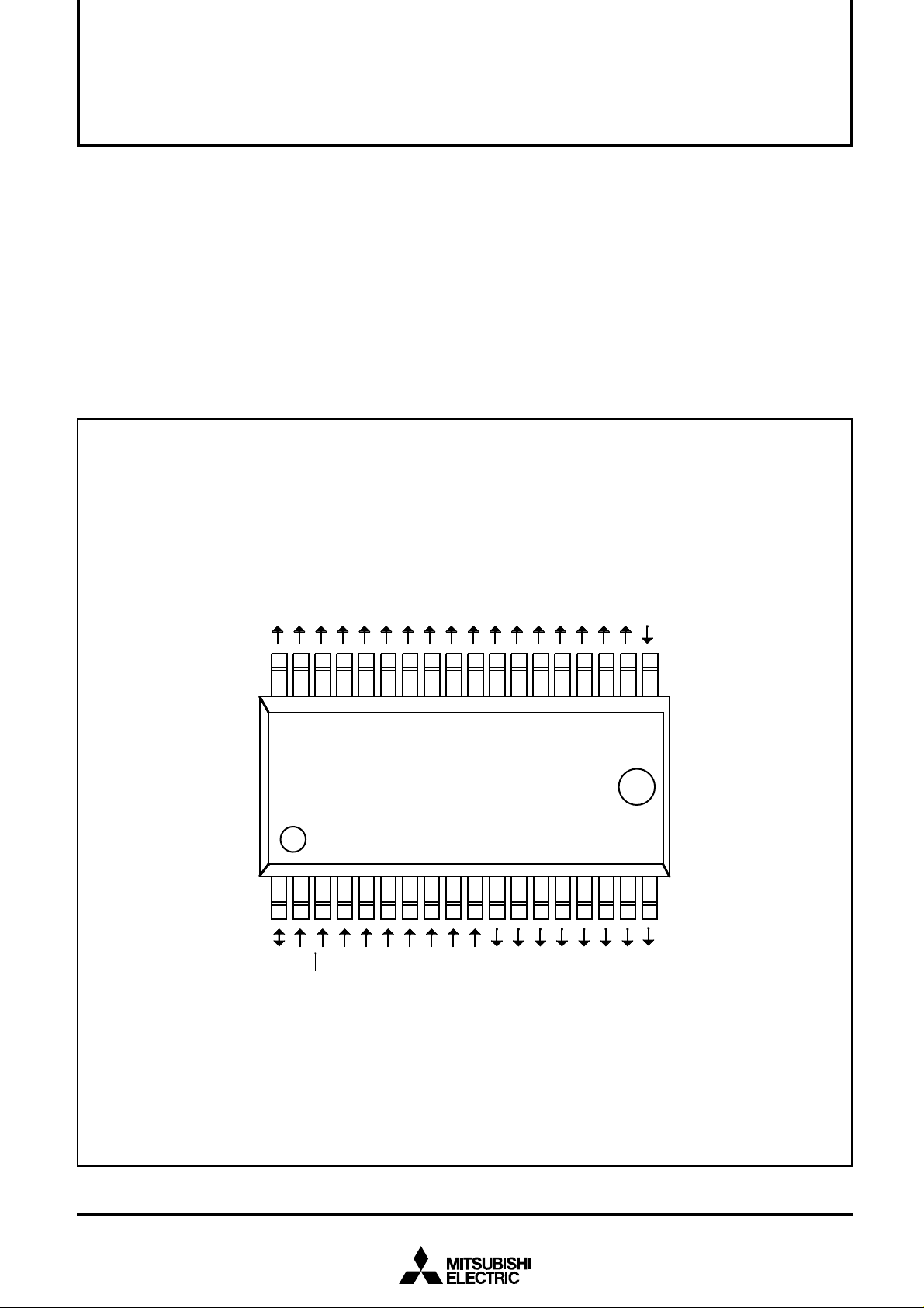
PIN CONFIGURATION (TOP VIEW)
FLD0
FLD1
FLD2
FLD3
FLD4
FLD5
Serial I/O ..................................... 3 (CS controller, external clock)
•
• Noise filter.....................................................built-in
(in serial input pin and clock pin, 2 MHz sampling)
• FLD display data ............................................. input
• A-D conversion data ..................................... output
• Command ....................................................... input
Package ......................................................................... 36P2R-G
•
Oscillation circuit ........... CR oscillation cirucit (external capacitor)
•
• Oscillation frequency.....................................2 MHz
Power source voltage.................................................. 4.0 to 5.5 V
•
FLD6
FLD7
FLD8
FLD9
FLD10
FLD11
FLD12
FLD13
FLD14
FLD15
FLD16
VEE
3635343332313029282726252423222120
M35502AFP
1
2
3
4
5
6
7
8
9
101112131415161718
SDATA
SCLK
CS
3
AN
CC
VSS
AN2
AN1
AN0
OSC
V
FLD24/P0
23/P1
FLD
22/P2
FLD
21
FLD
FLD20
FLD19
FLD18
19
FLD17
Fig.1 Pin configuration of M35502AFP
Package type: 36P2R-G
FUNCTIONAL BLOCK
/
MITSUBISHI LINEAR IC’s
M35502AFP
FLD CONTROLLER
V
EE
FLD
16
FLD
17
FLD
18
FLD
19
FLD
20
FLD
21
FLD22/P2
23
/P1
FLD
24
/P0
FLD
19
20
18
17
16
15
14
13
12
11
21
FLD15–FLD
25242322
Memory
address
8
Mode
register
Transfer
counter
FLD7–FLD
282726
0
3635343332313029
Display control circuit
Display RAM
DATA
S
CLK
CS
V
CC
V
SS
1
2
3
10
8
S
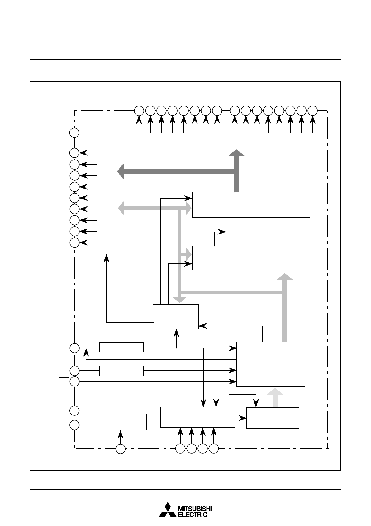
Fig.2 Functional block diagram
Noise filter
Noise filter
Clock generating
circuit
9
OSC
Command
analytic circuit
Selector
A-D control circuit
4
567
AN3–AN
Byte end
Serial I/O
Trigger
A-D
0
2
h
h
MITSUBISHI LINEAR IC’s
M35502AFP
FLD CONTROLLER
PIN DESCRIPTION
Table 1 Pin description
Pin
VCC, VSS
VEE
OSC
____
CS
SCLK
SDAT A
FLD24/P0 –
FLD22/P2
FLD21–
FLD0
Name
Power source
Pull-down
power source
Clock input
Chip select
Serial clock
Serial input/
output
Digit/Port
Segment/Digit
Input
Input
CMOS input
CMOS input
Noise filter
CMOS input
Noise filter
Output
N-channel
open-drain
P-channel
open-drain
P-channel
open-drain
• Apply voltage of 5 V to VCC, and 0 V to VSS.
• Applies voltage supplied to pull-down resistors.
• Connect an external capacitor to this pin.
• Serial transfer is possible by inputting “L” signal.
• Pull-up resistor is built in.
• Clock for serial transfer is input.
•
Read a clock twice with 2 MHz sampling clock and judge if it is a noise or not.
• Serial data is input/output.
•
In input mode, read a clock twice with 2 MHz sampling clock and judge if it is a
noise or not.
• Pin for ordinary output or digit output.
• At reset this port is set to VEE level through a pull-down resistor.
• Pin for digit output or segment output.
• At reset this port is set to VEE level through a pull-down resistor.
Function
PORT BLOCK
(1) Digit/Port pin
(2) Segmen/Digit pin
Segment/Digit data
✽ High-breakdown-voltage P-channel transistor
Note: Dimmer signal is for setting the Toff time.
Data bus
Digit data
Dimmer signal
(Note)
Latc
Dimmer signal
(Note)
Latc
(3) S
DATA
pin
Serial output
✽
V
EE
Serial input
(4) CS pin
Noise filter
CS input
(5) S
CLK
pin
✽
V
EE
Serial clock input
Noise filter
(6) A-D input
A-D conversion input
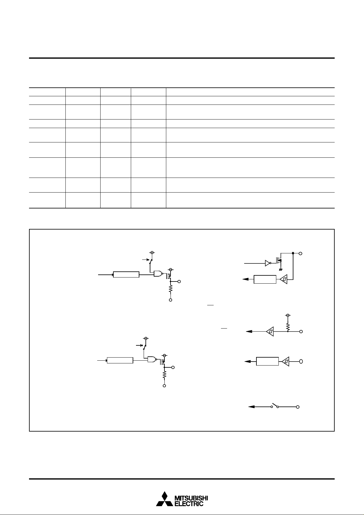
Fig.3 Port block diagram
3
COMMAND STYLE
b0b1b2b3b4b5b6
b7
MITSUBISHI LINEAR IC’s
M35502AFP
FLD CONTROLLER
Display data setting
(Command 0)
Display state setting
(Command 1)
111
a4
1 1 0 M1 M0M2M3M4
a1
a0a2a3
Digit start pin setting
0 0 0 0 : FLD
0 0 0 1 : FLD
0 0 1 0 : FLD
0 0 1 1 : FLD
0 1 0 0 : FLD
0 1 0 1 : FLD
0 1 1 0 : FLD
0 1 1 1 : FLD
1 0 0 0 : FLD
1 0 0 1 : FLD
1 0 1 0 : FLD
Serial data transfer setting
1 : 3-byte transfer
0 : 4-byte transfer
Display ON or OFF setting
1 : ON
0 : OFF
Display duty setting
1 1 : 15/16
1 0 : 6/16
0 1 : 4/16
0 0 : 3/16
18
17
16
15
14
13
12
11
10
9
8
Number of timing
selecting
(Command 2)
Port data setting
(Command 3)
Note:
DIG/PORT switch setting becomes valid when command 3 (port data setting) is accepted. When command 3
is not used, set “11
1 0 T3 T2 T1 T0
1–
100––p2p1p0
2
” to these bits.
DIG/PORT switch setting (Note )
0 0 : P0 output of command 3 valid
0 1 : P0, P1 output of command 3 valid
1 0 : P0, P1, P2 output of command 3
valid
1 1 : All port is set as DIG.
Number of timing setting
0 0 0 0 : T16
0 0 0 1 : T15
0 0 1 0 : T14
0 0 1 1 : T13
0 1 0 0 : T12
0 1 0 1 : T11
0 1 1 0 : T10
0 1 1 1 : T9
1 0 0 0 : T8
1 0 0 1 : T7
1 0 1 0 : T6
1 0 1 1 : T5
P2–P0 output data
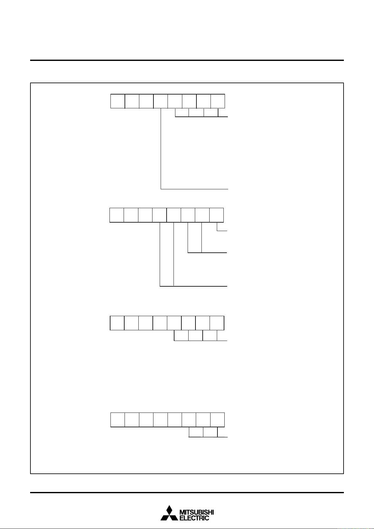
Fig.4 Command style
4
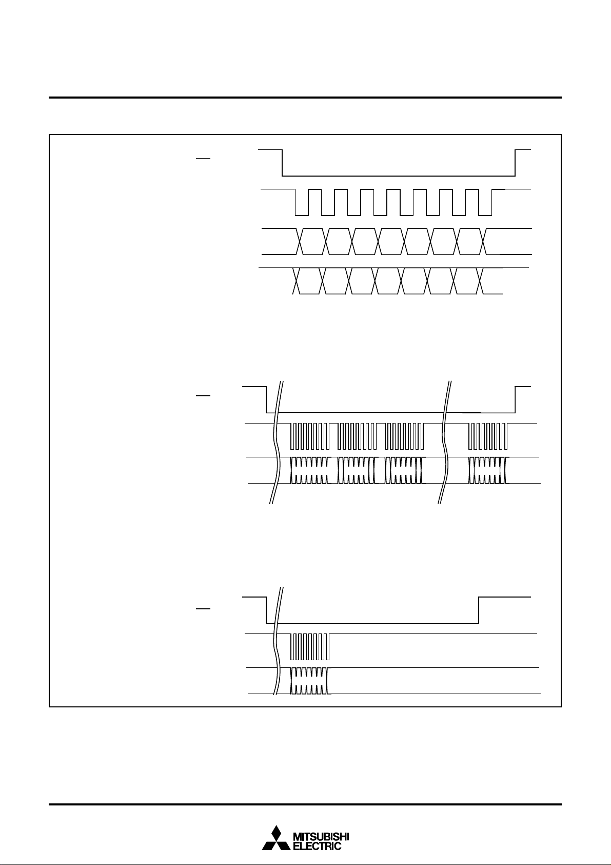
SERIAL I/O PROTOCOL
Byte protocol
MITSUBISHI LINEAR IC’s
M35502AFP
FLD CONTROLLER
CS
CLK
Command protocol
Display data setting
(Command 0)
Other setting except
display data setting
(Command 1 to 3)
S
DATA
DATA
S
CS
CLK
S
DATA
(input)
(output)
Note: S
(input)
Notes 1: The serial data which is transmitted after executing command
2: Set the CS signal to “H” level after transferring a display data.
b0 b1 b2 b3 b4 b5 b6 b7
b0 b1 b2 b3 b4 b5 b6 b7
DATA
is in high-impedance state during CS signal is “H”.
Command 0 Data 1 Data 2
0 is recognized as a display data.
Data i
Fig.5 Serial I/O protocol
CS
CLK
S
DATA
(input)
Command
5
 Loading...