Mitsubishi M35047-XXXSP, M35047-XXXFP Datasheet
MITSUBISHI MICROCOMPUTERS
M35047-XXXSP/FP
SCREEN CHARACTER and PATTERN DISPLAY CONTROLLERS
DESCRIPTION
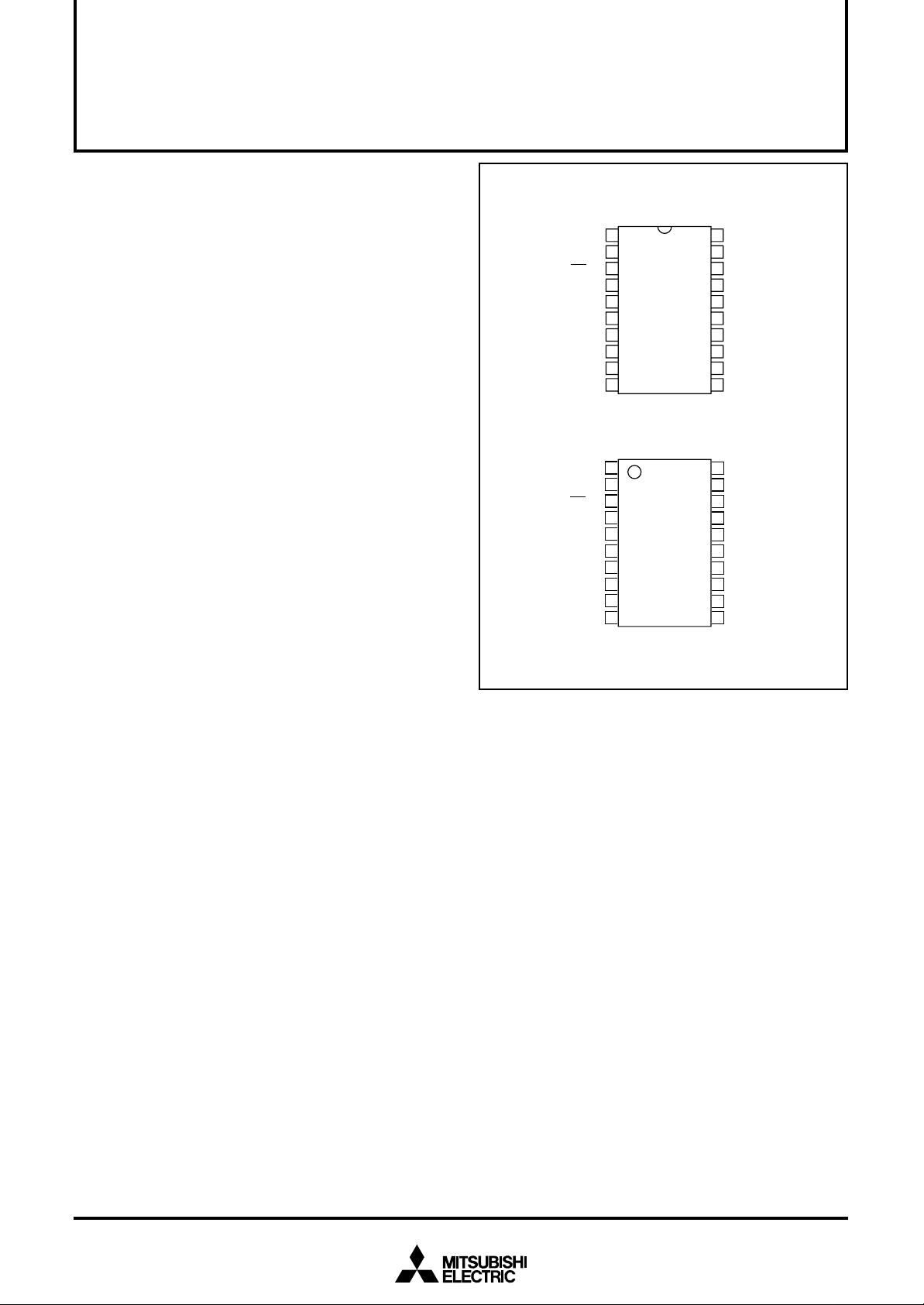
The M35047-XXXSP/FP is a character pattern display control IC
can display on the CRT display the liquid crystal display and the
plasma display. It uses a silicon gate CMOS process and it
housed in a 20-pin shrink DIP package (M35047-XXXSP) or a 20pin shrink SOP package (M35047-XXXFP).
For M35047-002SP/FP that is a standard ROM version of
M35047-XXXSP/FP respectively, the character pattern is also
mentioned.
FEATURES
Screen composition................................ 24 characters ✕ 12 lines
•
Number of characters displayed...................................288 (Max.)
•
Character composition .....................................12 ✕ 18 dot matrix
•
Characters available.....................ROM character:255 characters
•
Character sizes available ....................4 (vertical) ✕ 4 (horizontal)
•
Display locations available
•
Horizontal direction .............................................. 2007 locations
Vertical direction .................................................. 2047 locations
Blinking..................................................................Character units
•
Cycle : division of vertical synchronization signal into 32 or 64
Duty : 25%, 50%, or 75%
Data input ............................. By the I2C-BUS serial input function
•
Coloring for ROM character
•
Character color .....................................8 colors (Character unit)
Background coloring .............................8 colors (Character unit)
Border (shadow) coloring .....................8 colors (unit of screen /
Raster coloring.......................................8 colors (unit of screen)
Blanking for ROM character
•
Character size blanking
RAM character:8 characters
character unit)
Border size blanking
Matrix-outline blanking
All blanking (all raster area)
PIN CONFIGURATION (TOP VIEW)
CPOUT
V
SS2
AC
TEST
SCL
SDA
TCK
VDD1
P6
P7
1
←
2
→
3
→
4
→
5
↔
6
→
7
8
9
←
10
←
M35047-XXXSP
20
19
18
17
16
15
14
13
12
11
DD2
V
←
VERT
←
HOR
→
P5/B
→
P4
→
P3/G
→
P2
→
P1/R
→
P0/BLNK0
V
SS1
Outline 20P4B
CPOUT
SS2
V
AC
TEST
SCL
SDA
TCK
VDD1
P6
P7
←
2
→
3
→
4
→
5
↔
6
→
7
8
←
9
10
←
M35047-XXXFP
20
19
18
17
16
15
14
13
12
11
DD2
V
←
VERT
←
HOR
→
P5/B
→
P4
→
P3/G
→
P2
→
P1/R
→
P0/BLNK0
V
SS1
1
Outline 20P2Q-A
Coloring for RAM character................................8 colors (dot by dot)
•
Blanking for RAM character
•
Character size blanking
Matrix-outline blanking
All blanking (all raster area)
Output ports
•
4 shared output ports (toggled between RGB output)
4 dedicated output ports
Display RAM erase function
•
Display input frequency range....... FOSC = 20.0MHz to 100.0MHz
•
Horizontal synchronous input frequency
•
........................................................H.sync = 15 kHz to 130 kHz
Display oscillation stop function
•
APPLICATION
CRT display, Liquid crystal display, Plasma display
Rev.1.2

PIN DESCRIPTION
Pin
Number
1
Symbol
CPOUT
Pin name
Filter output
Input/
Output
Output
MITSUBISHI MICROCOMPUTERS
M35047-XXXSP/FP
SCREEN CHARACTER and PATTERN DISPLAY CONTROLLERS
Function
Filter output. Connect loop filter to this pin.
2
3
4
5
6
7
8
9
10
11
12
13
14
15
16
17
VSS2
__
AC
TEST
SCL
SDA
TCK
VDD1
P6
P7
VSS1
P0/BLNK0
P1/R
P2
P3/G
P4
P5/B
Earthing pin
Auto-clear input
Test input
Clock input
Data I/O
External clock
Power pin
Port P6 output
Port P7 output
Earthing pin
Port P0 output
Port P1 output
Port P2 output
Port P3 output
Port P4 output
Port P5 output
–
Input
Input
Input
I/O
Input
–
Output
Output
–
Output
Output
Output
Output
Output
Output
Connect to GND.
When “L”, this pin resets the internal IC circuit. Hysteresis input. Built-in pull-up resistor.
Test pin. Connect to +5V.
SDA pin serial data is taken in when SCL rises. Hysteresis input.
This is the pin for serial input of display control register and display RAM data. Also, this
pin output acknowledge signal. Hysteresis input. Nch opendrain output.
This is the pin for external clock input.
Please connect to +5V with the power pin.
This is the output port.
This is the output port.
Please connect to GND using circuit earthing pin.
This pin can be toggled between port pin output and BLNK0 signal output.
This pin can be toggled between port pin output and R signal output.
This is the output port.
This pin can be toggled between port pin output and G signal output.
This is the output port.
This pin can be toggled between port pin output and B signal output.
18
19
20
HOR
VERT
VDD2
Horizontal synchronous signal input
Vertical synchronous signal input
Power pin
Input
Input
–
This pin inputs the horizontal synchronous signal. Hysteresis input.
This pin inputs the vertical synchronous signal. Hysteresis input.
Please connect to +5V with the power pin.
2
5
7
6
8
20
4
SCL
SDA
V
DD1
V
DD2
3AC
11V
SS12VSS2
TEST
Clock oscillation
circuit display
Timing generator
Polarity switching circuit
Address control
circuit
Data control
circuit
Display control
register
Display RAM
Shift register
Blinking circuit
Reading address
control circuit
Display location
detection circuit
H counter
TCK
1
CPOUT
18
HOR
19
12
VERT
Synchronous signal
switching circuit
Display control
circuit
Port output
control circuit
P0/BLNK0
13 P1/R
15 P3/G
17 P5/B
14 P2
16 P4
9P6
10 P7
Input control circuit
Polarity switching circuit
Display character
RAM
Display character
ROM
MITSUBISHI MICROCOMPUTERS
M35047-XXXSP/FP
SCREEN CHARACTER and PATTERN DISPLAY CONTROLLERS
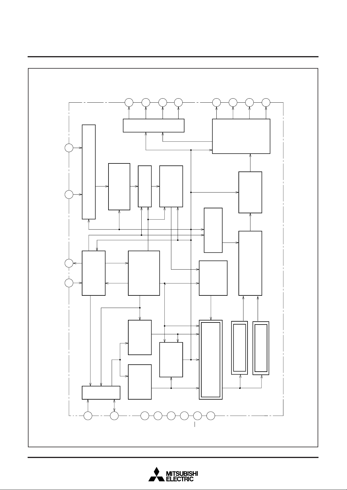
BLOCK DIAGRAM
3
MITSUBISHI MICROCOMPUTERS
M35047-XXXSP/FP
SCREEN CHARACTER and PATTERN DISPLAY CONTROLLERS
MEMORY CONSTITUTION
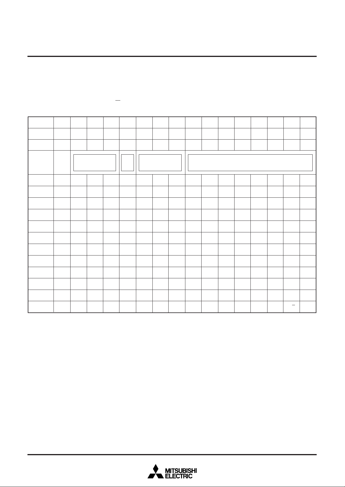
Address 00016 to 11F16 are assigned to the display RAM, address
12016 to 12916 are assigned to the display control registers and
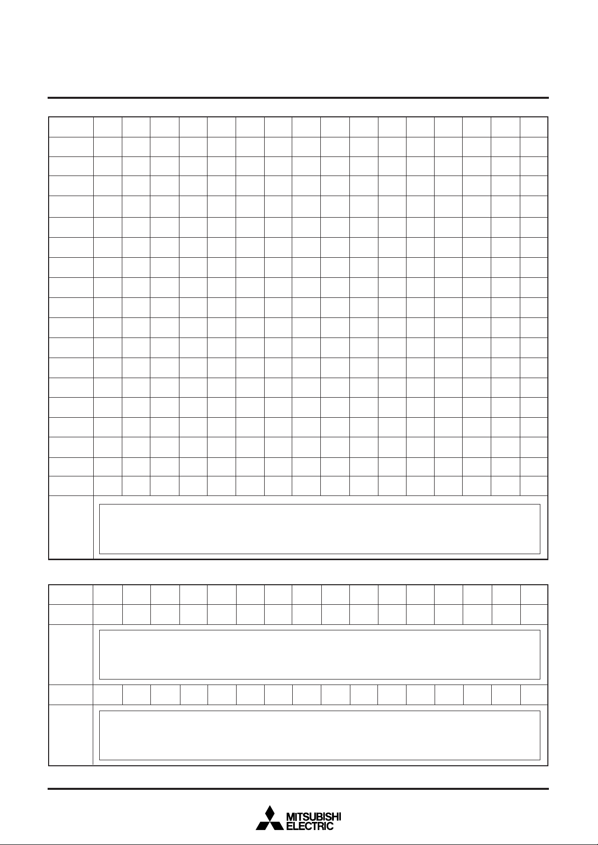
address 20016 to 2F116 are assigned to the RAM characters. The
internal circuit is reset and all display control registers (address
12016 to 12916) are set to "0" when the AC pin level is "L". And
Addresses
00016
00116
11E16
11F16
12016
12116
12216
DAF DAE DAD DAC DAB DAA DA9 DA8 DA7 DA6 DA5 DA4 DA3 DA2 DA1 DA0
0 BB BG BR BLINK B G R C7 C6 C5 C4 C3 C2 C1 C0
0 BB BG BR BLINK B G R C7 C6 C5 C4 C3 C2 C1 C0
………
………
Background
coloring
Blink-
ing
Character color
0 BB BG BR BLINK B G R C7 C6 C5 C4 C3 C2 C1 C0
0 BB BG BR BLINK B G R C7 C6 C5 C4 C3 C2 C1 C0
0
SPACE2 SPACE1 SPACE0
TEST10 DIV10 DIV9 DIV8 DIV7 DIV6 DIV5 DIV4 DIV3 DIV2 DIV1 DIV0
0 EXCK1 EXCK0 RSEL1 RSEL0 DIVS2 DIVS1 DIVS0 PTC7 PTC6 PTC5 PTC4 PTC3 PTC2 PTC1 PTC0
0 TEST17 TEST16 TEST15 TEST14 TEST13 TEST12 TEST11 PTD7 PTD6 PTD5 PTD4 PTD3 PTD2 PTD1 PTD0
then, RAM is not erased and be undefinited. For detail, see "DATA
INPUT EXAMPLE". Memory constitution is shown in Figure 1 to 9.
Character code
12316
12416
12516
12616
12716
12816
12916
0 TEST3 TEST2 TEST1 TEST0 HP10 HP9 HP8 HP7 HP6 HP5 HP4 HP3 HP2 HP1 HP0
0 TEST20
0 TEST23 TEST22 TEST21 DSP11 DSP10 DSP9 DSP8 DSP7 DSP6 DSP5 DSP4 DSP3 DSP2 DSP1 DSP0
0 TEST24
0 TEST25
0 TEST29 HSZ21 HSZ20 HSZ11 HSZ10
0 TEST30 BLINK2 BLINK1 BLINK0
RBLK0
TEST19 TEST18 VP10 VP9 VP8 VP7 VP6 VP5 VP4 VP3 VP2 VP1 VP0
VSZ1H1 VSZ1H0 VSZ1L1 VSZ1L0
VSZ2H1 VSZ2H0 VSZ2L1 VSZ2L0
V1SZ1 V1SZ0 LIN9 LIN8 LIN7 LIN6 LIN5 LIN4 LIN3 LIN2
V18SZ1 V18SZ0 LIN17 LIN16 LIN15 LIN14 LIN13 LIN12 LIN11 LIN10
BETA14
TEST28 TEST27 TEST26 FB FG FR RB RG RR
DSPON
STOP
RAMERS
Fig.1 Memory constitution (Display RAM, Display Control register)
SYAD BLK1 BLK0 POLH POLV VMASK B/F BCOL
4
MITSUBISHI MICROCOMPUTERS
M35047-XXXSP/FP
SCREEN CHARACTER and PATTERN DISPLAY CONTROLLERS
Address
20016
20116
20216
20316
20416
20516
20616
20716
20816
20916
20A16
20B16
20C16
20D16
DAF DAE DAD DAC DAB DAA DA9 DA8 DA7 DA6 DA5 DA4 DA3 DA2 DA1 DA0
0BSGSRSFR000B FR000A FR0009 FR0008 FR0007 FR0009 FR0005 FR0004 FR0003 FR0002 FR0001 FR0000
0BSGSRSFR001B FR001A FR0019 FR0018 FR0017 FR0019 FR0015 FR0014 FR0013 FR0012 FR0011 FR0010
0BSGSRSFR002B FR002A FR0029 FR0028 FR0027 FR0026 FR0025 FR0024 FR0023 FR0022 FR0021 FR0020
0BSGSRSFR003B FR003A FR0039 FR0038 FR0037 FR0036 FR0035 FR0034 FR0033 FR0032 FR0031 FR0030
0BSGSRSFR004B FR004A FR0049 FR0048 FR0047 FR0046 FR0045 FR0044 FR0043 FR0042 FR0041 FR0040
0BSGSRSFR005B FR005A FR0059 FR0058 FR0057 FR0056 FR0055 FR0054 FR0053 FR0052 FR0051 FR0050
0BSGSRSFR006B FR006A FR0069 FR0068 FR0067 FR0066 FR0065 FR0064 FR0063 FR0062 FR0061 FR0060
0BSGSRSFR007B FR007A FR0079 FR0078 FR0077 FR0076 FR0075 FR0074 FR0073 FR0072 FR0071 FR0070
0BSGSRSFR008B FR008A FR0089 FR0088 FR0087 FR0086 FR0085 FR0084 FR0083 FR0082 FR0081 FR0080
0BSGSRSFR009B FR009A FR0099 FR0098 FR0097 FR0096 FR0095 FR0094 FR0093 FR0092 FR0091 FR0090
0BSGSRSFR00AB FR00AA FR00A9 FR00A8 FR00A7 FR00A6 FR00A5 FR00A4 FR00A3 FR00A2 FR00A1 FR00A0
0BSGSRSFR00BB FR00BA FR00B9 FR00B8 FR00B7 FR00B6 FR00B5 FR00B4 FR00B3 FR00B2 FR00B1 FR00B0
0BSGSRSFR00CB FR00CA FR00C9 FR00C8 FR00C7 FR00C6 FR00C5 FR00C4 FR00C3 FR00C2 FR00C1 FR00C0
0BSGSRSFR00DB FR00DA FR00D9 FR00D8 FR00D7 FR00D6 FR00D5 FR00D4 FR00D3 FR00D2 FR00D1 FR00D0
20E16
20F16
21016
21116
21216
0BSGSRSFR00EB FR00EA FR00E9 FR00E8 FR00E7 FR00E6 FR00E5 FR00E4 FR00E3 FR00E2 FR00E1 FR00E0
0BSGSRSFR00FB FR00FA FR00F9 FR00F8 FR00F7 FR00F6 FR00F5 FR00F4 FR00F3 FR00F2 FR00F1 FR00F0
0BSGSRSFR010B FR010A FR0109 FR0108 FR0107 FR0106 FR0105 FR0104 FR0103 FR0102 FR0101 FR0100
0BSGSRSFR011B FR011A FR0119 FR0118 FR0117 FR0116 FR0115 FR0114 FR0113 FR0112 FR0111 FR0110
........................
21F16
Fig.2 Memory constitution (RAM character 0)
Address
22016
22116
23016
23116
23216
DAF DAE DAD DAC DAB DAA DA9 DA8 DA7 DA6 DA5 DA4 DA3 DA2 DA1 DA0
0BSGSRSFR100B FR100A FR1009 FR1008 FR1007 FR1006 FR1005 FR1004 FR1003 FR1002 FR1001 FR1000
0BSGSRSFR111B FR111A FR1119 FR1118 FR1117 FR1116 FR1115 FR1114 FR1113 FR1112 FR1111 FR1110
Can not be used
RAM character 1 data
23F16
Fig.3 Memory constitution (RAM character 1)
Can not be used
5

MITSUBISHI MICROCOMPUTERS
M35047-XXXSP/FP
SCREEN CHARACTER and PATTERN DISPLAY CONTROLLERS
Address
24016
24116
DAF DAE DAD DAC DAB DAA DA9 DA8 DA7 DA6 DA5 DA4 DA3 DA2 DA1 DA0
0BSGSRSFR200B FR200A FR2009 FR2008 FR2007 FR2006 FR2005 FR2004 FR2003 FR2002 FR2001 FR2000
................
25016
25116
25216
25F16
Fig.4 Memory constitution (RAM character 2)
Address
26016
26116
0BSGSRSFR211B FR211A FR2119 FR2118 FR2117 FR2116 FR2115 FR2114 FR2113 FR2112 FR2111 FR2110
DAF DAE DAD DAC DAB DAA DA9 DA8 DA7 DA6 DA5 DA4 DA3 DA2 DA1 DA0
0BSGSRSFR300B FR300A FR3009 FR3008 FR3007 FR3006 FR3005 FR3004 FR3003 FR3002 FR3001 FR3000
........
27016
RAM character 2 data
Can not be used
RAM character 3 data
27116
27216
0BSGSRSFR311B FR311A FR3119 FR3118 FR3117 FR3116 FR3115 FR3114 FR3113 FR3112 FR3111 FR3110
........
27F16
Fig.5 Memory constitution (RAM character 3)
Address
28016
28116
DAF DAE DAD DAC DAB DAA DA9 DA8 DA7 DA6 DA5 DA4 DA3 DA2 DA1 DA0
0BSGSRSFR400B FR400A FR4009 FR4008 FR4007 FR4006 FR4005 FR4004 FR4003 FR4002 FR4001 FR4000
................
29016
29116
29216
29F16
0BSGSRSFR411B FR411A FR4119 FR4118 FR4117 FR4116 FR4115 FR4114 FR4113 FR4112 FR4111 FR4510
Can not be used
RAM character 4 data
Can not be used
Fig.6 Memory constitution (RAM character 4)
6

MITSUBISHI MICROCOMPUTERS
M35047-XXXSP/FP
SCREEN CHARACTER and PATTERN DISPLAY CONTROLLERS
Address
2A016
2A116
DAF DAE DAD DAC DAB DAA DA9 DA8 DA7 DA6 DA5 DA4 DA3 DA2 DA1 D00
0BSGSRSFR500B FR500A FR5009 FR5008 FR5007 FR5006 FR5005 FR5004 FR5003 FR5002 FR5001 FR5000
................
2B016
2B116
2B216
2BF16
Fig.7 Memory constitution (RAM character 5)
Address
2C016
2C116
0BSGSRSFR511B FR511A FR5119 FR5118 FR5117 FR5116 FR5115 FR5114 FR5113 FR5112 FR5111 FR5110
DAF DAE DAD DAC DAB DAA DA9 DA8 DA7 DA6 DA5 DA4 DA3 DA2 DA1 DA0
0BSGSRSFR600B FR600A FR6009 FR6008 FR6007 FR6006 FR6005 FR6004 FR6003 FR6002 FR6001 FR6000
........
2D016
RAM character 5 data
Can not be used
RAM character 6 data
2D116
2D216
0BSGSRSFR611B FR611A FR6119 FR6118 FR6117 FR6116 FR6115 FR6114 FR6113 FR6112 FR6111 FR6110
........
2DF16
Fig.8 Memory constitution (RAM character 6)
Address
2E016
2E116
DAF DAE DAD DAC DAB DAA DA9 DA8 DA7 DA6 DA5 DA4 DA3 DA2 DA1 DA0
0BSGSRSFR700B FR700A FR7009 FR7008 FR7007 FR7006 FR7005 FR7004 FR7003 FR7002 FR7001 FR7000
........
2F016
2F116
Fig.9 Memory constitution (RAM character 7)
0BSGSRSFR711B FR711A FR7119 FR7118 FR7117 FR7116 FR7115 FR7114 FR7113 FR7112 FR7111 FR7110
Can not be used
RAM character 7 data
7
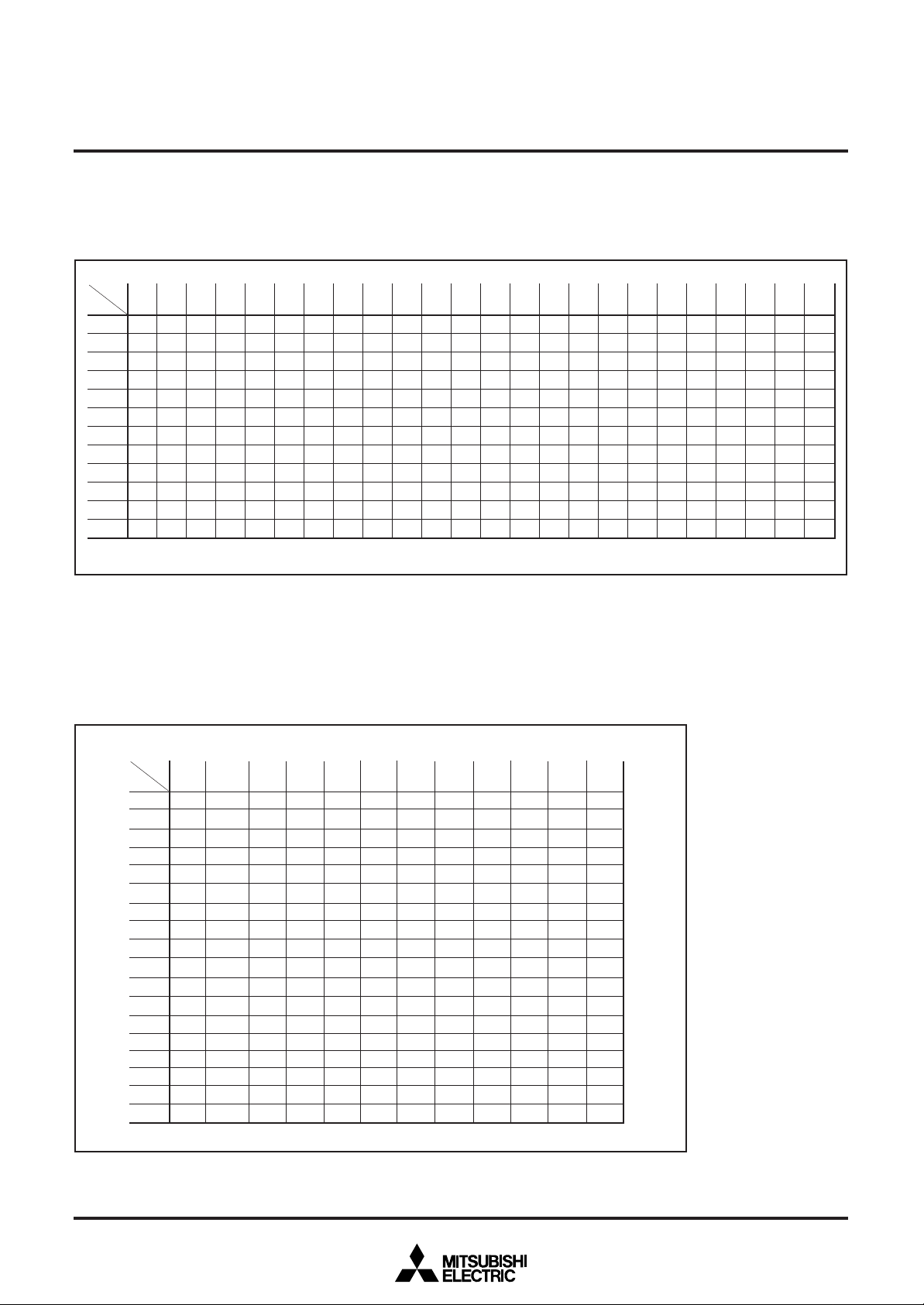
SCREEN CONSTITUTION
The screen lines and rows are determined from each address of
the display RAM . The screen constitution is shown in Figure 10.
Row
Line
1 2 3 4 5 6 7 8 9 101112131415161718192021222324
0001600116002160031600416005160061600716008160091600A1600B1600C1600D1600E1600F1601016011160121601316014160151601616017
1
018160191601A1601B1601C1601D1601E1601F160201602116022160231602416025160261602716028160291602A1602B1602C1602D1602E1602F
2
3
0301603116032160331603416035160361603716038160391603A1603B1603C1603D1603E1603F1604016041160421604316044160451604616047
4
048160491604A1604B1604C1604D1604E1604F160501605116052160531605416055160561605716058160591605A1605B1605C1605D1605E1605F
5
0601606116062160631606416065160661606716068160691606A1606B1606C1606D1606E1606F1607016071160721607316074160751607616077
6
078160791607A1607B1607C1607D1607E1607F160801608116082160831608416085160861608716088160891608A1608B1608C1608D1608E1608F
7
0901609116092160931609416095160961609716098160991609A1609B1609C1609D1609E1609F160A0160A1160A2160A3160A4160A5160A6160A7
8
0A8160A9160AA160AB160AC160AD160AE160AF160B0160B1160B2160B3160B4160B5160B6160B7160B8160B9160BA160BB160BC160BD160BE160BF
9
0C0160C1160C2160C3160C4160C5160C6160C7160C8160C9160CA160CB160CC160CD160CE160CF160D0160D1160D2160D3160D4160D5160D6160D7
10
0D8160D9160DA160DB160DC160DD160DE160DF160E0160E1160E2160E3160E4160E5160E6160E7160E8160E9160EA160EB160EC160ED160EE160EF
11
0F0160F1160F2160F3160F4160F5160F6160F7160F8160F9160FA160FB160FC160FD160FE160FF1610016101161021610316104161051610616107
12
108161091610A1610B1610C1610D1610E1610F161101611116112161131611416115161161611716118161191611A1611B1611C1611D1611E1611F
✽ The hexadecimal numbers in the boxes show the display RAM address.
MITSUBISHI MICROCOMPUTERS
M35047-XXXSP/FP
SCREEN CHARACTER and PATTERN DISPLAY CONTROLLERS
16
16
16
16
16
16
16
16
16
16
16
16
Fig.10 Screen constitution
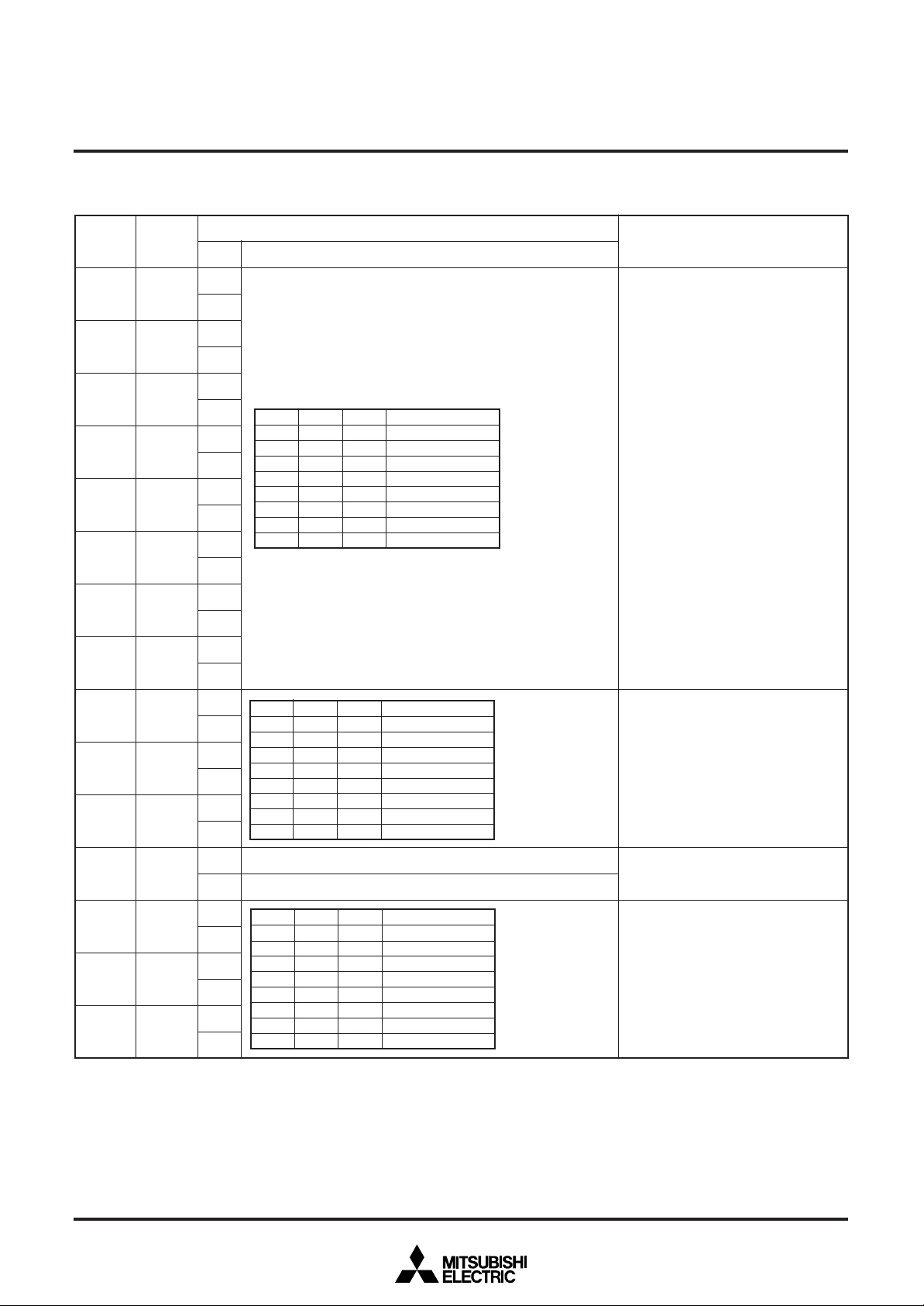
RAM Character CONSTITUTION
The dot lines and dot rows of the character RAM are determined
from each address and bit of the character RAM . The RAM character constitution is shown in Figure 11.
Dot
Dot
10
11
12
13
14
15
16
17
18
✽ The number in the boxes show the bit address of the RAM character :n. ("n" is RAM number : 0 to 7)
Fig.11 RAM charcter consititution
Note. When the RAM character is used, it is necessary to clear all areas of the RAM character first.
123456789101112
FRn00B FRn00A FRn009 FRn008 FRn007 FRn006 FRn005 FRn004 FRn003 FRn002 FRn001 FRn000
1
FRn01B FRn01A FRn019 FRn018 FRn017 FRn016 FRn015 FRn014 FRn013 FRn012 FRn011 FRn010
2
FRn02B FRn02A FRn029 FRn028 FRn027 FRn026 FRn025 FRn024 FRn023 FRn022 FRn021 FRn020
3
FRn03B FRn03A FRn039 FRn038 FRn037 FRn036 FRn035 FRn034 FRn033 FRn032 FRn031 FRn030
4
FRn04B FRn04A FRn049 FRn048 FRn047 FRn046 FRn045 FRn044 FRn043 FRn042 FRn041 FRn040
5
FRn05B FRn05A FRn059 FRn058 FRn057 FRn056 FRn055 FRn054 FRn053 FRn052 FRn051 FRn050
6
FRn06B FRn06A FRn069 FRn068 FRn067 FRn066 FRn065 FRn064 FRn063 FRn062 FRn061 FRn060
7
FRn07B FRn07A FRn079 FRn078 FRn077 FRn076 FRn075 FRn074 FRn073 FRn072 FRn071 FRn070
8
FRn08B FRn08A FRn089 FRn088 FRn087 FRn086 FRn085 FRn084 FRn083 FRn082 FRn081 FRn080
9
FRn09B FRn09A FRn099 FRn098 FRn097 FRn096 FRn095 FRn094 FRn093 FRn092 FRn091 FRn090
FRn0AB FRn0AA FRn0A9 FRn0A8 FRn0A7 FRn0A6 FRn0A5 FRn0A4 FRn0A3 FRn0A2 FRn0A1 FRn0A0
FRn0BB FRn0BA FRn0B9 FRn0B8 FRn0B7 FRn0B6 FRn0B5 FRn0B4 FRn0B3 FRn0B2 FRn0B1 FRn0B0
FRn0CB FRn0CA FRn0C9 FRn0C8 FRn0C7 FRn0C6 FRn0C5 FRn0C4 FRn0C3 FRn0C2 FRn0C1 FRn0C0
FRn0DB FRn0DA FRn0D9 FRn0D8 FRn0D7 FRn0D6 FRn0D5 FRn0D4 FRn0D3 FRn0D2 FRn0D1 FRn0D0
FRn0EB FRn0EA FRn0E9 FRn0E8 FRn0E7 FRn0E6 FRn0E5 FRn0E4 FRn0E3 FRn0E2 FRn0E1 FRn0E0
FRn0FB FRn0FA FRn0F9 FRn0F8 FRn0F7 FRn0F6 FRn0F5 FRn0F4 FRn0F3 FRn0F2 FRn0F1 FRn0F0
FRn10B FRn10A FRn109 FRn108 FRn107 FRn106 FRn105 FRn104 FRn103 FRn102 FRn101 FRn100
FRn11B FRn11A FRn119 FRn118 FRn117 FRn116 FRn115 FRn114 FRn113 FRn112 FRn111 FRn110
8
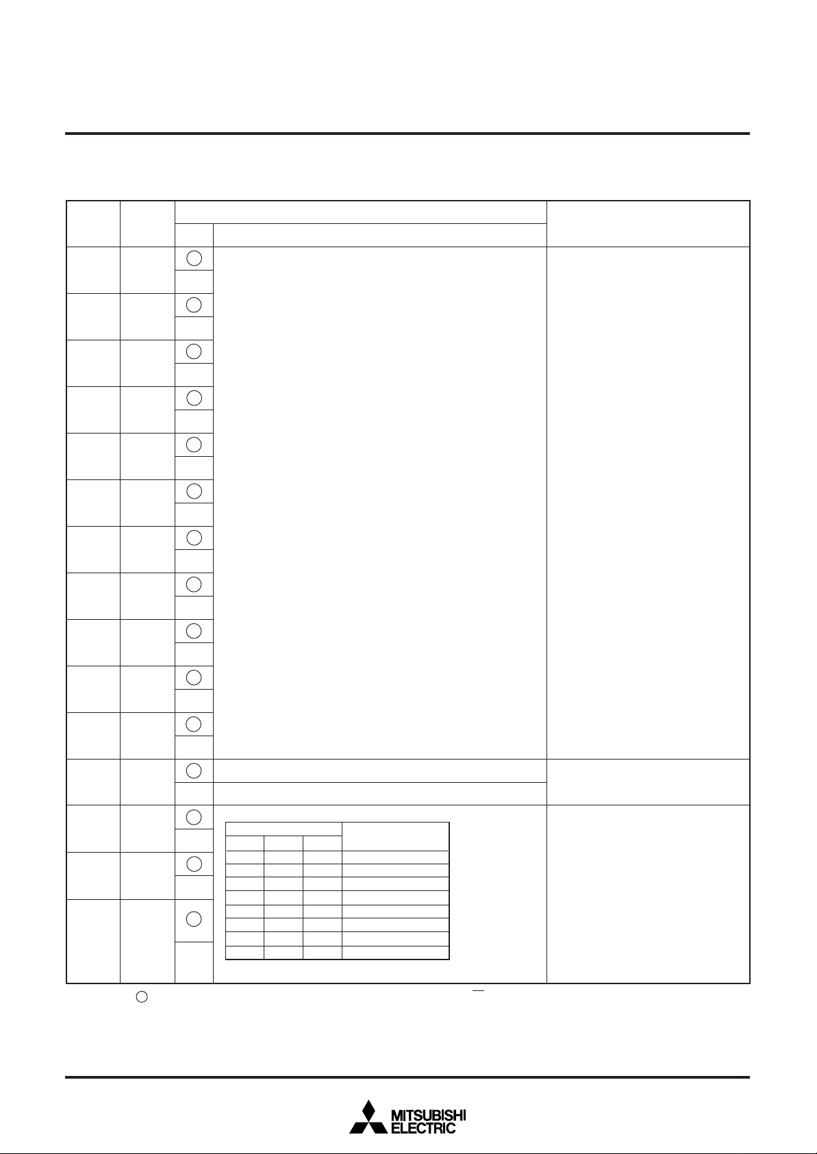
DISPLAY RAM
Address 00016 to 11F16
DA
Register
0
1
2
3
4
5
C0
C1
C2
C3
C4
C5
SCREEN CHARACTER and PATTERN DISPLAY CONTROLLERS
Contents
Status
0
Set the displayed ROM character code.
1
0
*RAM character is selected using the 8 bits from C7 to C0.
When C7 to C0=(111111102) is set. And, RAM character code
1
is set to R, G and B.
0
1
0
1
0
1
0
G
B
0
0
0
0
1
1
1
1
R
0
0
0
1
1
0
1
1
0
0
0
1
1
0
1
1
1
Function
RAM character code
RAM character 0
RAM character 1
RAM character 2
RAM character 3
RAM character 4
RAM character 5
RAM character 6
RAM character 7
MITSUBISHI MICROCOMPUTERS
M35047-XXXSP/FP
Remarks
Set display character
6
C6
1
0
0
7
C7
1
8
R
1
0
0
9
G
1
0
A
B
1
Do not blink.
B
BLINK
0
1
Blinking
0
C
BR
1
0
D
BG
1
0
E
BB
1
Note. The display RAM is undefined state at the AC pin.
B
BB
G
0
0
0
0
1
0
1
0
0
1
0
1
1
1
1
1
BG
0
0
0
0
0
1
0
1
1
0
1
0
1
1
1
1
____
BR
R
0
1
0
1
0
1
0
1
Color
Black
Red
Green
Yellow
Blue
Magenta
Cyan
White
Set character color (character unit)
* When set C7 to C0= (111111102), can
be set RAM character code.
Set blinking
See register BLINK2 to BLINK0 (address12916)
0
1
0
1
0
1
0
1
Color
Black
Red
Green
Yellow
Blue
Magenta
Cyan
White
Set character background color.
(character unit)
*When set C7 to C0=(111111102)
and register RBLK0
(address 12416)= “1”, set coloring
prohibition color.
Moreover, when the blink is set, the
parts other than the color set by this
register are blinks.
See DISPLAY FORM 2.
9
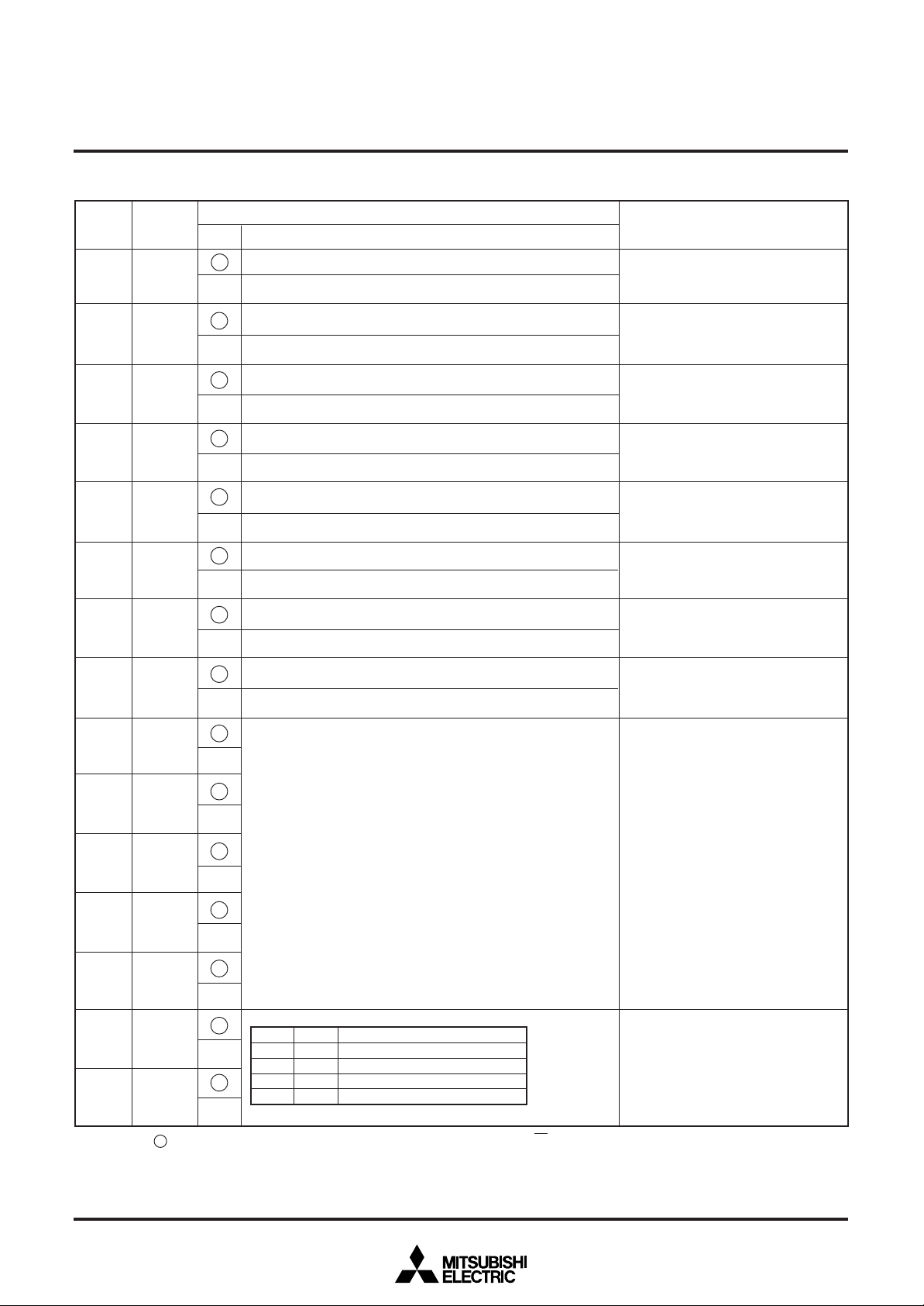
REGISTERS DESCRIPTION
(1) Address 12016
MITSUBISHI MICROCOMPUTERS
M35047-XXXSP/FP
SCREEN CHARACTER and PATTERN DISPLAY CONTROLLERS
DA
0
1
2
3
4
5
6
7
8
Register
DIV0
DIV1
DIV2
DIV3
DIV4
DIV5
DIV6
DIV7
DIV8
Contents
Status
0
Set division value (multiply value) of horizontal oscillation frequency.
Function
1
0
1
0
10
N1 =
(DIVn ✕ 2n)
Σ
n = 0
N1 : division value (multiply value)
1
0
1
0
1
0
1
0
1
0
1
0
1
Remarks
Set display frequency by division value
(multiply value) setting.
For details, see REGISTER
SUPPLEMENTARY DESCRIPTION
(1).
Also, set the display frequency range by
registers DIVS0, DIVS1, DIVS2, RSEL0
and RSEL1(address 12116) in accordance with the display frequency.
Any of this settings above is required
only when EXCK1 = 0, EXCK0 = 1 and
EXCK1 = 1, EXCK0 = 1.
9
DIV9
1
0
0
A
DIV10
1
0
TEST10
B
SPACE0
C
SPACE1
D
E
SPACE2
Note. The mark around the status value means the reset status by the "L" level is input to AC pin.
It should be fixed to "0".
1
Can not be used.
0
1
0
1
0
1
SPACE
2
1
0
0
0
0
0
1
0
1
1
0
1
0
1
1
1
1
(S) represents one line worth of space
Number of Lines and Space
<(S) represents space>
0
0
1
0
1
0
1
0
1
1 (S) 10 (S) 1
2 (S) 8 (S) 2
3 (S) 6 (S) 3
4 (S) 4 (S) 4
5 (S) 2 (S) 5
6 (S) 6
6 (S)(S) 6
12
Leave one line worth of space in the vertical direction.
For example, 6 (S) 6 indicates two sets
of 6 lines with a line of spaces between
lines 6 and 7.
A line is 18 ✕ N horizontal scan lines.
N is determined by the character size in
the vertical direction
10
(2) Address 12116
MITSUBISHI MICROCOMPUTERS
M35047-XXXSP/FP
SCREEN CHARACTER and PATTERN DISPLAY CONTROLLERS
DA
Register
Status
0
0
1
2
3
4
5
6
PTC0
PTC1
PTC2
PTC3
PTC4
PTC5
PTC6
P0 output (port P0).
1
BLNK0 output.
0
P1 output (port P1).
1
R signal output.
0
P2 output (port P2).
1
Can not be used.
0
P3 output (port P3).
1
G signal output.
0
P4 output (port P4).
1
Can not be used.
0
P5 output (port P5).
1
B signal output.
0
P6 output (port P6).
1
Can not be used.
Function
P0 pin output control.
P1 pin output control.
P2 pin output control.
P3 pin output control.
P4 pin output control.
P5 pin output control.
P6 pin output control.
Remarks
Contents
0
7
8
PTC7
DIVS0
P7 output (port P7).
1
Can not be used.
0
For setting, see REGISTER SUPPLEMENTARY DESCRIPTION
(2).
P7 pin output control.
Set display frequency range.
1
0
9
DIVS1
1
0
A
DIVS2
1
0
B
RSEL0
1
0
C
RSEL1
1
0
D
EXCK0
1
0
E
EXCK1
1
EXCK1
0
0
1
1
EXCK0
0
External synchronous (external clock)
1
0
1
Display clock input
Internal synchronous
Do not set
External synchronous (internal clock)
Display clock setting
See REGISTER SUPPLEMENTARY
DESCRIPTION (1)
Note. The mark around the status value means the reset status by the "L" level is input to AC pin.
11
(3) Address 12216
DA
Register
0
1
2
3
PTD0
PTD1
PTD2
PTD3
SCREEN CHARACTER and PATTERN DISPLAY CONTROLLERS
Contents
Status
0
"L" output or negative polarity output (BLNK0 output).
1
"H" output or positive polarity output (BLNK0 output).
0
"L" output or negative polarity output (R signal output).
1
"H" output or positive polarity output (R signal output).
0
"L" output.
1
"H" output.
0
"L" output or negative polarity output (G signal output).
1
"H" output or positive polarity output (G signal output).
Function
MITSUBISHI MICROCOMPUTERS
M35047-XXXSP/FP
Remarks
P0 pin data control.
P1 pin data control.
P2 pin data control.
P3 pin data control.
0
4
5
6
7
8
9
A
B
PTD4
PTD5
PTD6
PTD7
TEST11
TEST12
TEST13
TEST14
"L" output.
1
"H" output.
0
"L" output or negative polarity output (B signal output).
1
"H" output or positive polarity output (B signal output).
0
"L" output.
1
"H" output.
0
"L" output.
1
"H" output.
0
Can not be used.
1
It should be fixed to "1".
0
It should be fixed to "0".
1
Can not be used.
0
It should be fixed to "0".
1
Can not be used.
0
It should be fixed to "0".
1
Can not be used.
P4 pin data control.
P5 pin data control.
P6 pin data control.
P7 pin data control.
0
C
TEST15
D
TEST16
E
TEST17
Note. The mark around the status value means the reset status by the "L" level is input to AC pin.
12
It should be fixed to "0".
1
Can not be used.
0
It should be fixed to "0".
1
Can not be used.
0
It should be fixed to "0".
1
Can not be used.
(4) Address 12316
DA
Register
0
1
2
3
4
5
HP0
HP1
HP2
HP3
HP4
HP5
Status
0
1
0
1
0
1
0
1
0
1
0
1
SCREEN CHARACTER and PATTERN DISPLAY CONTROLLERS
Contents
Function
If HS is the horizontal display start location,
HS = T ✕ ( 2nNPn+m)
T: Period of display frequency
2007 settings are possible.
m : offset value differ for the setting of the register EXCK0 and
EXCK1. It shown below.
EXCK1
EXCK0
10
Σ
n = 0
001 1
010 1
m
13 13 Do not set 19
HOR
MITSUBISHI MICROCOMPUTERS
M35047-XXXSP/FP
Remarks
Horizontal display start location is specified using the 11 bits from HP10 to HP0.
HP10 to HP0 = (000000000002) and
(000001001112) setting is forbidden.
HS*(shown left) shows horizontal display start location this is register B/F
(address 12916) = "0" is set.
6
HP6
0
VS
1
7
8
HP7
HP8
0
1
VERT
0
HS*
Display area
1
9
HP9
0
1
A
HP10
0
1
0
B
C
D
E
TEST0
TEST1
TEST2
TEST3
It should be fixed to "0".
1
Can not be used.
0
It should be fixed to "0".
1
Can not be used.
0
It should be fixed to "0".
1
Can not be used.
It should be fixed to "0".
0
Can not be used.
1
Note. The mark around the status value means the reset status by the "L" level is input to AC pin.
13
 Loading...