Mitsubishi M35046-XXXSP, M35046-XXXFP Datasheet
MITSUBISHI MICROCOMPUTERS
M35046-XXXSP/FP
SCREEN CHARACTER and PATTERN DISPLAY CONTROLLERS
DESCRIPTION
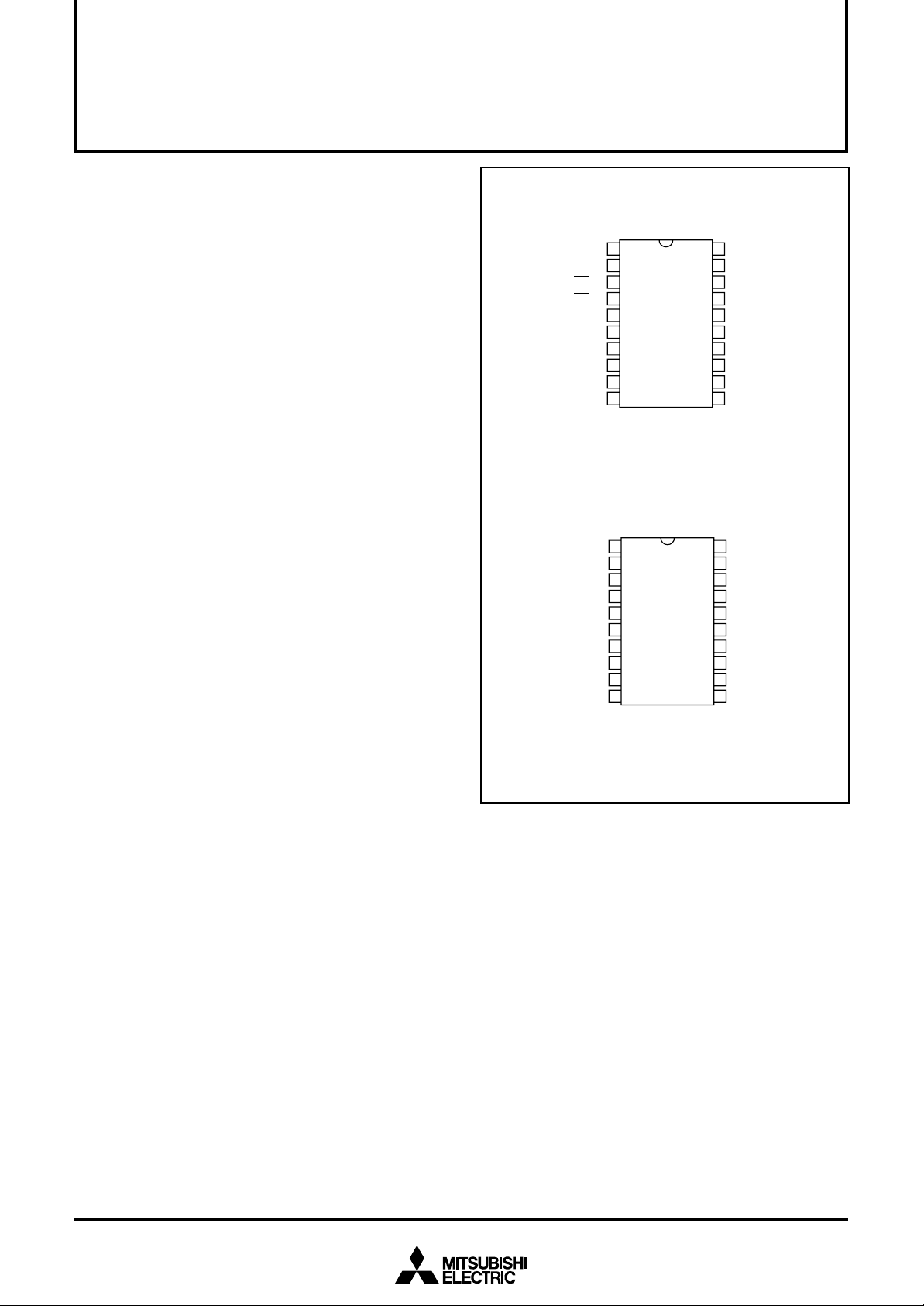
The M35046-XXXSP/FP is a character pattern display control IC can
display on the liquid crystal display and the plasma display. It uses a
silicon gate CMOS process and it housed in a 20-pin shrink DIP package (M35046-XXXSP) or a 20-pin shrink SOP package (M35046XXXFP).
For M35046-001SP/FP that is a standard ROM version of M35046XXXSP/FP respectively, the character pattern is also mentioned.
FEATURES
Screen composition .................................... 24 columns × 12 lines
•
Number of characters displayed................................... 288 (Max.)
•
Character composition ..................................... 12 × 18 dot matrix
•
Characters available.............................................. 256 characters
•
Character sizes available .................... 4 (horizontal) × 4 (vertical)
•
Display locations available
•
Horizontal direction.............................................. 1000 locations
Vertical direction .................................................. 1023 locations
Blinking.................................................................. Character units
•
Cycle : division of vertical synchronization signal into 32 or 64
Duty : 25%, 50%, or 75%
Data input .................................. By the 16-bit serial input function
•
Coloring
•
Character color ..................................................... Character unit
Background coloring............................................. Character unit
Matrix-outline (shadow) coloring.............. 8 colors (RGB output)
Specified by register
Border coloring ........................................ 8 colors (RGB output)
Specified by register
Raster coloring ........................................ 8 colors (RGB output)
Specified by register
Blanking Character size blanking
•
Border size blanking
Matrix-outline blanking
All blanking (all raster area)
Output ports
•
4 shared output ports (toggled between RGB output)
4 dedicated output ports
Display RAM erase function
•
Display input frequency range............... FOSC = 20MHz to 80MHz
•
Horizontal synchronous input frequency
•
........................................................H.sync = 15 kHz to 130 kHz
Display oscillation stop function
•
PIN CONFIGURATION (TOP VIEW)
CPOUT
VSS2
AC
CS
SCK
SIN
TCK
DD1
V
P6
P7
←
1
@
2
→
3
→
4
→
5
→
6
→
7
@
8
←
9
←
10
M35046 - XXXSP
20
19
18
17
16
15
14
13
12
11
@
DD2
V
←
VERT
←
HOR
→
P5/B
→
P4
→
P3/G
→
P2
→
P1/R
→
P0/BLNK0
@
SS
V
Outline 20P4B
@
CPOUT
VIR
AC
CS
SCK
SIN
TCK
DD1
V
P6
P7
←
1
@
2
→
3
→
4
→
5
→
6
→
7
@
8
←
9
←
10
M35046 - XXXFP
20
19
18
17
16
15
14
13
12
11
V
DD2
←
VERT
←
HOR
→
P5/B
→
P4
→
P3/G
→
P2
→
P1/R
→
P0/BLNK0
@
V
SS1
Outline 20P2Q-A
APPLICATION
Liquid crystal display, Plasma display, Video projecter
Rev.1.1
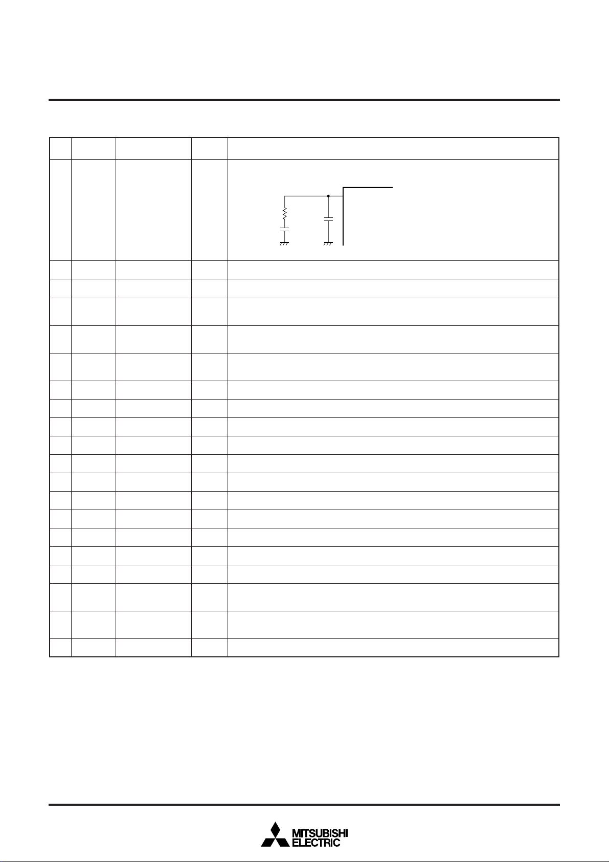
PIN DESCRIPTION
1.0kΩ∗1
0.01µF
∗
2
47pF
∗
2
CPOUT
∗
1 Use at 1% precision
∗
2 Use at 10% precision
1pin
MITSUBISHI MICROCOMPUTERS
M35046-XXXSP/FP
SCREEN CHARACTER and PATTERN DISPLAY CONTROLLERS
Pin
Number
1
2
3
4
5
6
7
8
9
Symbol
CPOUT
VSS2
__
AC
__
CS
SCK
SIN
TCK
VDD1
P6
Pin name
Phase difference
Earthing pin
Auto-clear input
Chip select input
Serial clock input
Serial data input
External clock
Power pin
Port P6 output
Input/
Output
Output
–
Input
Input
Input
Input
Input
–
Output
Function
Connect loop filter to this pin.
Connect to GND.
When “L”, this pin resets the internal IC circuit. Hysteresis input. Built-in pull-up resistor.
This is the chip select input pin, and when serial data transmission is being carried out, it
goes to “L”. Hysteresis input. Built-in pull-up resistor.
__
When CS pin is “L”, SIN serial data is taken in when SCK rises. Hysteresis input. Built-in
pull-up resistor.
This is the pin for serial input of data and addresses for the display control register and
the display data memory. Hysteresis input. Built-in pull-up resistor.
This is the pin for external clock input.
Please connect to +5V with the power pin.
This is the output port. Port data is set by PTD6.
10
11
12
13
14
15
16
17
18
19
20
P7
VSS1
P0/BLNK0
P1/R
P2
P3/G
P4
P5/B
HOR
VERT
VDD2
Port P7 output
Earthing pin
Port P0 output
Port P1 output
Port P2 output
Port P3 output
Port P4 output
Port P5 output
Horizontal synchro-
nous signal input
Vertical synchro-
nous signal input
Power pin
Output
–
Output
Output
Output
Output
Output
Output
Input
Input
–
This is the output port. Port data is set by PTD7.
Please connect to GND using circuit earthing pin.
This pin can be toggled between port pin output and BLNK0 signal output.
This pin can be toggled between port pin output and R signal output.
This is the output port. Port data is set by PTD2.
This pin can be toggled between port pin output and G signal output.
This is the output port. Port data is set by PTD4.
This pin can be toggled between port pin output and B signal output.
This pin inputs the horizontal synchronous signal. Hysteresis input.
This pin inputs the vertical synchronous signal. Hysteresis input.
Please connect to +5V with the power pin.
2
VERT
MITSUBISHI MICROCOMPUTERS
M35046-XXXSP/FP
SCREEN CHARACTER and PATTERN DISPLAY CONTROLLERS
P0/BLNK0
13 P1/R
15 P3/G
17 P5/B
12
circuti
Polarity
19
switching
14 P2
16 P4
Port output
9P6
control circuit
10 P7
18
HOR
CPOUT
7
TCK
Polarity switching circuit
Clock oscillation
circuit for display
Input control circuit
H counter
switching circuit
Synchronous signal
Timing generator
circuit
Address control
circuit
Data control
detection circuit
Display location
register
Display control
Blinking circuit
control circuit
Reading address
Display RAM
circuit
Display control
Display character ROM Shift register
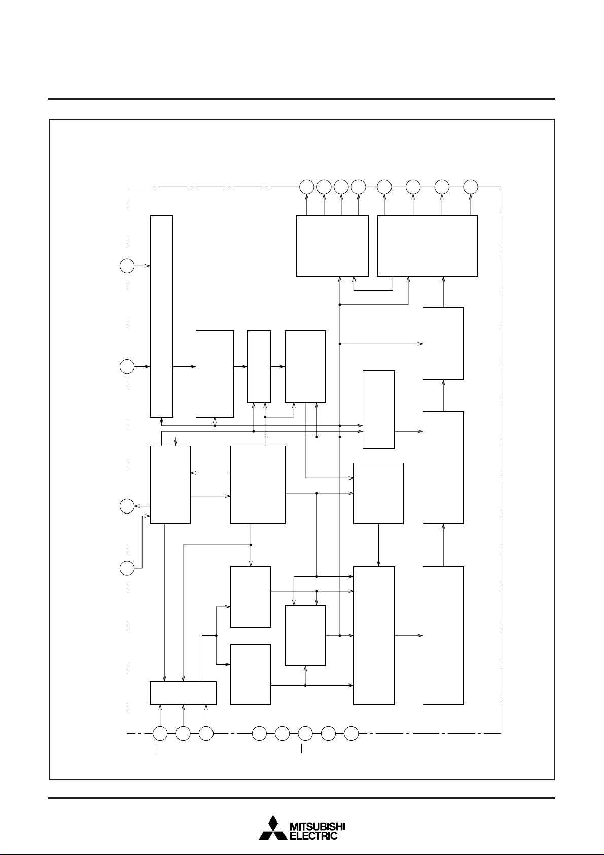
BLOCK DIAGRAM
415
CS
SCK
6
SIN
8
DD1
V
20
VDD2
3
AC
2
11
SS
VIR
V
3
MITSUBISHI MICROCOMPUTERS
M35046-XXXSP/FP
SCREEN CHARACTER and PATTERN DISPLAY CONTROLLERS
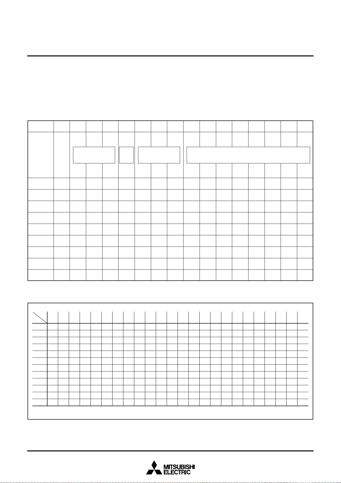
MEMORY CONSTITUTION
Address 00016 to 11F16 are assigned to the display RAM, address
12016 to 12816 are assigned to the display control registers. The internal circuit is reset and all display control registers (address 12016
to 12816) are set to “0” when the AC pin level is “L”. And then RAM is
erased.
Memory constitution is shown in Figure 1.
DAF DAE DAD DAC DAB DAA DA9 DA8 DA7 DA6 DA5 DA4 DA3 DA2 DA1 DA0
00016
………
11F16
12016
12116
12216
12316
12416
0 BB BG BR BLINK B G R C7 C6 C5 C4 C3 C2 C1 C0
………
0 BB BG BR BLINK B G R C7 C6 C5 C4 C3 C2 C1 C0
0 EXCK0 VJT DIVS1 DIVS0 DIV10 DIV9 DIV8 DIV7 DIV6 DIV5 DIV4 DIV3 DIV2 DIV1 DIV0
0 RSEL0 PTD7 PTD6 PTD5 PTD4 PTD3 PTD2 PTD1 PTD0 PTC5 PTC4 PTC3 PTC2 PTC1 PTC0
0 RSEL1
0 EXCK1 TEST3 TEST2 TEST1 TEST0 VP9 VP8 VP7 VP6 VP5 VP4 VP3 VP2 VP1 VP0
0
TEST14
__
Background
coloring
SPACE2 SPACE1 SPACE0
Blinking
Character color
TEST9 HP9 HP8 HP7 HP6 HP5 HP4 HP3 HP2 HP1 HP0
TEST5 TEST4 DSP11 DSP10 DSP9 DSP8 DSP7 DSP6 DSP5 DSP4 DSP3 DSP2 DSP1 DSP0
SCREEN CONSTITUTION
The screen lines and rows are determined from each address of the
display RAM. The screen constitution is shown in Figure 2.
Character code
12516
12616
12716
12816
0
TEST10
0
TEST11
0
TEST12
0
TEST13 BLINK2 BLINK1 BLINK0 DSPON
Fig. 1 Memory constitution
Row
Line
123456789101112131415161718192021222324
1
0001600116002160031600416005160061600716008160091600A1600B1600C1600D1600E1600F1601016011160121601316014160151601616017
2
018160191601A1601B1601C1601D1601E1601F160201602116022160231602416025160261602716028160291602A1602B1602C1602D1602E1602F
3
0301603116032160331603416035160361603716038160391603A1603B1603C1603D1603E1603F1604016041160421604316044160451604616047
4
048160491604A1604B1604C1604D1604E1604F160501605116052160531605416055160561605716058160591605A1605B1605C1605D1605E1605F
5
0601606116062160631606416065160661606716068160691606A1606B1606C1606D1606E1606F1607016071160721607316074160751607616077
6
078160791607A1607B1607C1607D1607E1607F160801608116082160831608416085160861608716088160891608A1608B1608C1608D1608E1608F
7
0901609116092160931609416095160961609716098160991609A1609B1609C1609D1609E1609F160A0160A1160A2160A3160A4160A5160A6160A7
8
0A8160A9160AA160AB160AC160AD160AE160AF160B0160B1160B2160B3160B4160B5160B6160B7160B8160B9160BA160BB160BC160BD160BE160BF
9
0C0160C1160C2160C3160C4160C5160C6160C7160C8160C9160CA160CB160CC160CD160CE160CF160D0160D1160D2160D3160D4160D5160D6160D7
10
0D8160D9160DA160DB160DC160DD160DE160DF160E0160E1160E2160E3160E4160E5160E6160E7160E8160E9160EA160EB160EC160ED160EE160EF
11
0F0160F1160F2160F3160F4160F5160F6160F7160F8160F9160FA160FB160FC160FD160FE160FF1610016101161021610316104161051610616107
12
108161091610A1610B1610C1610D1610E1610F161101611116112161131611416115161161611716118161191611A1611B1611C1611D1611E1611F
ƒ The hexadecimal numbers in the boxes show the display RAM address.
VSZ1H1 VSZ1H0 VSZ1L1 VSZ1L0
V1SZ1 V1SZ0 LIN9 LIN8 LIN7 LIN6 LIN5 LIN4 LIN3 LIN2
VSZ2H1 VSZ2H0 VSZ2L1 VSZ2L0 V18SZ1 V18SZ0
HSZ21 HSZ20 HSZ11 HSZ10
BETA14
TEST8 TEST7 TEST6 FB FG FR RB RG RR
STOP
RAMERS
LIN17 LIN16 LIN15 LIN14 LIN13 LIN12 LIN11 LIN10
SYAD BLK1 BLK0 POLH POLV
VMASK__B/F BCOL
16
16
16
16
16
16
16
16
16
16
16
16
Fig. 2 Screen constitution
4
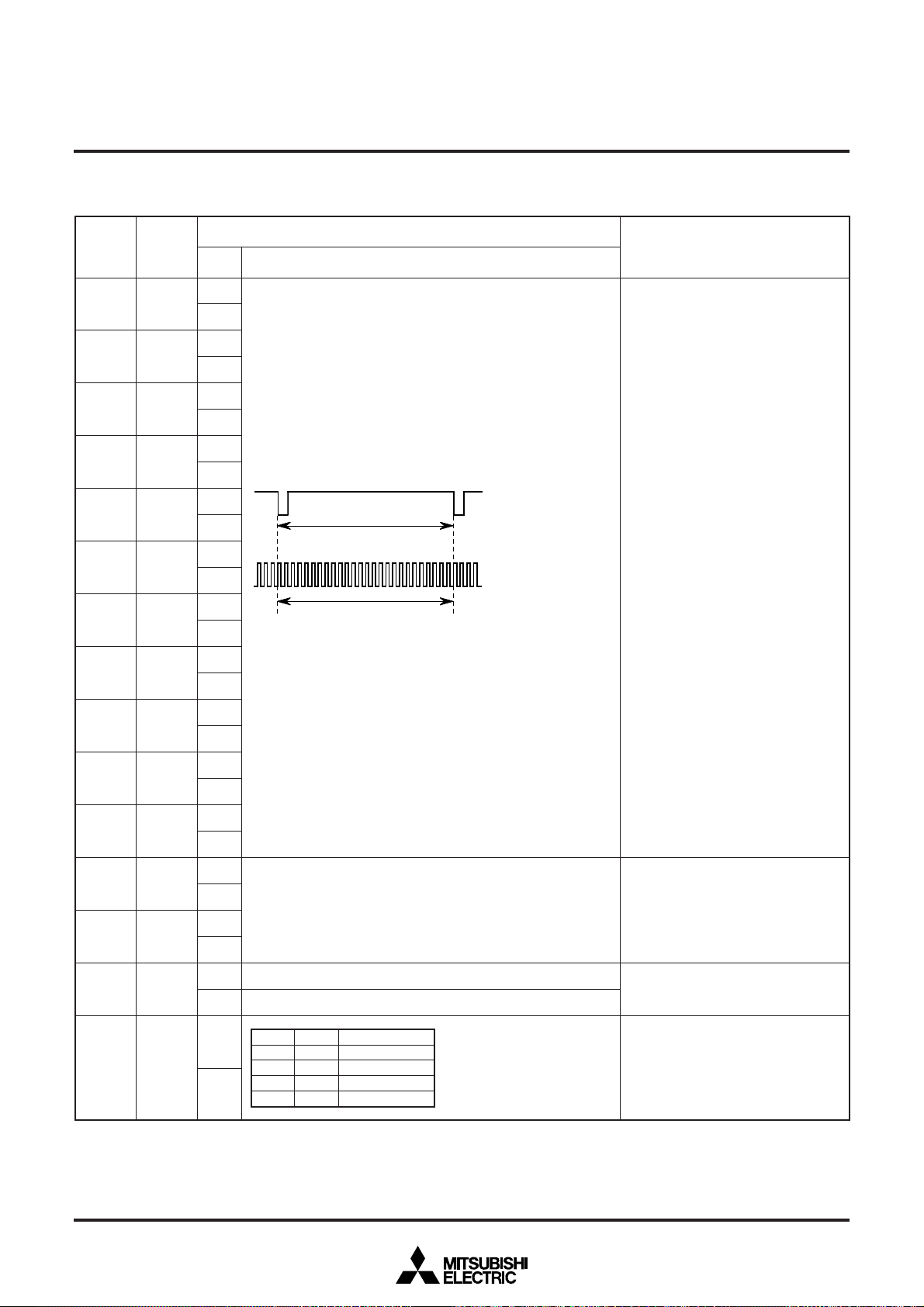
REGISTERS DESCRIPTION
)
(1) Address 12016
MITSUBISHI MICROCOMPUTERS
M35046-XXXSP/FP
SCREEN CHARACTER and PATTERN DISPLAY CONTROLLERS
RegisterDA
Status
0
0
DIV0
Set external clock frequency value of horizontal oscillation frequency.
1
0
1
DIV1
Function
Set display frequency by frequency
value setting. Set N1 to be “N1=fOSC/
fH”.
fOSC(MHz) : External clock frequency
1
2
DIV2
1
0
10
N1 = (DIVn × 2n)
Σ
n = 0
N1: frequency value
0
3
DIV3
1
H o r i z o n t a l s y n c h r o n i z e d s i g n a l
0
4
5
6
DIV4
DIV5
DIV6
1
0
1
0
E x t e r n a l c l o c k
1 H
( N 1
C l o c k n u m b e r
fH(kHz) : Horizontal synchronous sig-
Set registers DIVS0, DIVS1 (address
12016), RSEL0 (address 12116) and
RSEL1 (address 12216) according to
external clock frequency.
For details, see (2) Setting display frequencies under Register Supplementary Description.
Any of this settings above is reguired
only when EXCK1=1, EXCK0=1.
Remarks
for TCK pin (=display frequency)
nal frequency for HOR pin
1
0
Contents
7
DIV7
1
0
8
DIV8
1
0
9
DIV9
1
0
A
DIV10
1
0
B
DIVS0
For details, see (2) Setting display frequencies under Register
Supplementary Description.
1
Set display frequency area.
0
C
D
DIVS1
VJT
1
It should be fixed to “0”.
0
1
Alleviates continuous vertical jitters.
EXCK0
E
0
1
0
0
1
1
0
1
0
1
20 to 30MHz
Do not set
Do not set
20 to 80MHz
Display clock input
EXCK0
EXCK1
See setting External Clock Input Mode
(to be input from the TCK terminal).
EXCK1 : address 12316
5

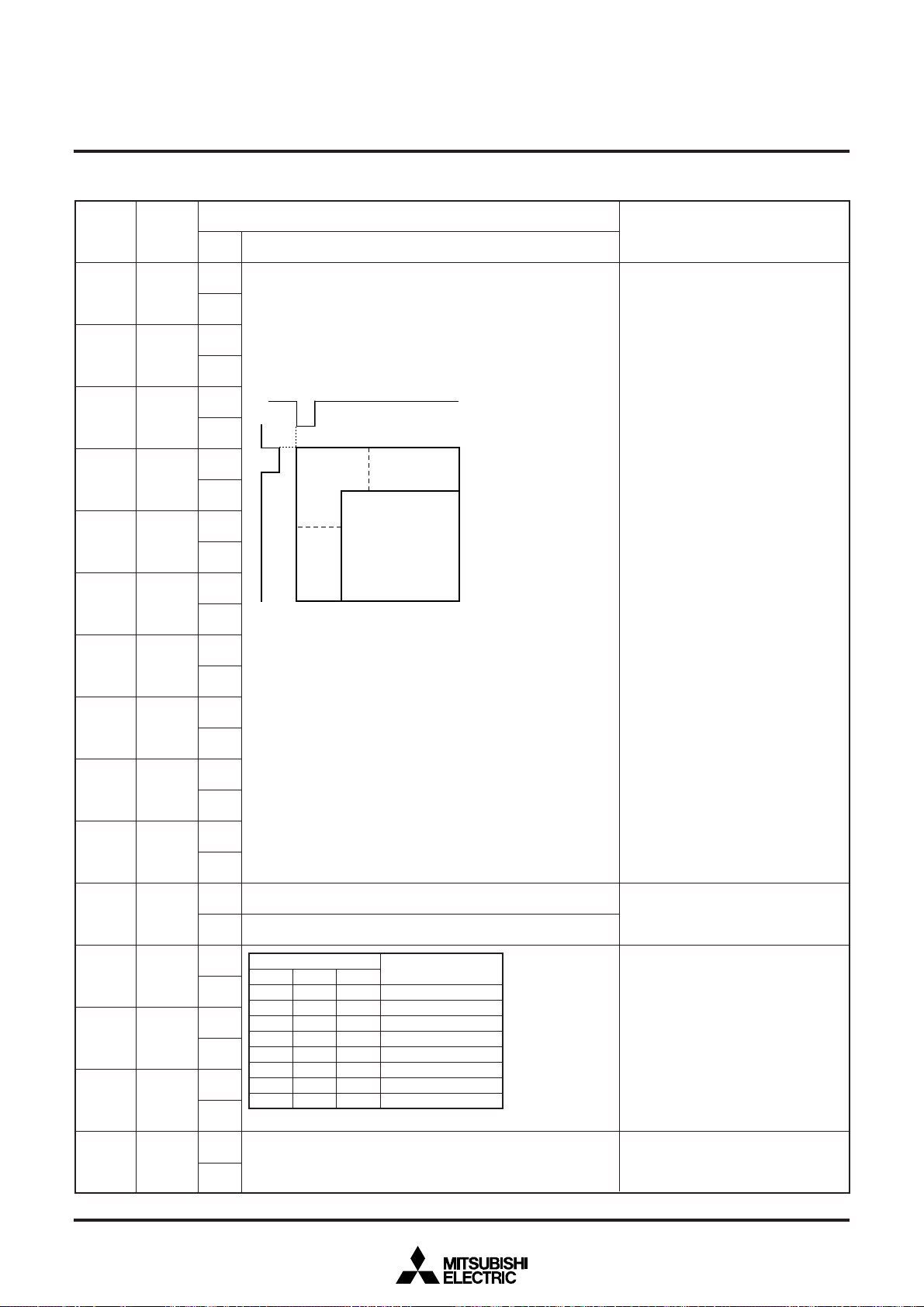
(2) Address 12116
MITSUBISHI MICROCOMPUTERS
M35046-XXXSP/FP
SCREEN CHARACTER and PATTERN DISPLAY CONTROLLERS
RegisterDA Remarks
0
1
2
3
4
5
6
PTC0
PTC1
PTC2
PTC3
PTC4
PTC5
PTD0
(Note)
Status Function
P0 output (port P0). Port data is set by PTD0.
0
BLNK0 output. Polarity is set by PTD0.
1
P1 output (port P1). Port data is set by PTD1.
0
R signal output. Polarity is set by PTD1.
1
P2 output (port P2). Port data is set by PTD2.
0
Can not be used.
1
P3 output (port P3). Port data is set by PTD3.
0
G signal output. Polarity is set by PTD3.
1
P4 output (port P4). Port data is set by PTD4.
0
Can not be used.
1
P5 output (port P5). Port data is set by PTD5.
0
B signal output. Polarity is set by PTD5.
1
“L” output (P0 output) or negative polarity output (BLNK0 output).
0
“H” output (P0 output) or positive polarity output (BLNK0 output).
1
Contents
BLNK0 outputs blanking signal.
Blanking status is determined by BLK0,
BLK1, and DSP0 to DSP11 settings.
P0 pin data control.
“L” output (P1 output) or negative polarity output (R signal output).
0
7
8
9
A
B
C
D
E
Note. To determined this register, input clock (at least one clock) to the external clock pin (TCK).
PTD1
(Note)
PTD2
(Note)
PTD3
(Note)
PTD4
(Note)
PTD5
(Note)
PTD6
(Note)
PTD7
(Note)
RSEL0
“H” output (P1 output) or positive polarity output (R signal output).
1
“L” output (P2 output).
0
“H” output (P2 output).
1
“L” output (P3 output) or negative polarity output (G signal output).
0
“H” output (P3 output) or positive polarity output (G signal output).
1
“L” output (P2 output).
0
“H” output (P2 output).
1
“L” output (P5 output) or negative polarity output (B signal output).
0
“H” output (P5 output) or positive polarity output (B signal output).
1
“L” output (P6 output).
0
“H” output (P6 output).
1
“L” output (P7 output).
0
“H” output (P7 output).
1
For details, see (2) Setting display frequencies under Register
0
Supplementary Description.
To be used when EXCK0=1 and EXCK1=1.
1
P1 pin data control.
P2 pin exclusive port output state control.
P3 pin data control.
P4 pin exclusive port output state control.
P5 pin data control.
P6 pin exclusive port output state control.
P7 pin exclusive port output state control.
Set display frequency area.
6
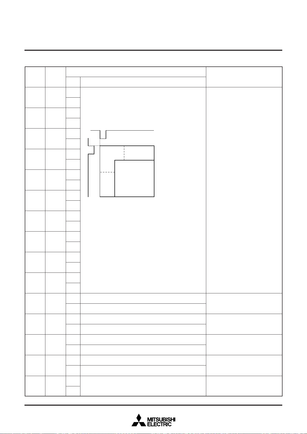
(3) Address 12216
MITSUBISHI MICROCOMPUTERS
M35046-XXXSP/FP
SCREEN CHARACTER and PATTERN DISPLAY CONTROLLERS
Register
Status
0
0
1
HP0
(LSB)
HP1
If HS is the horizontal display start location,
1
HS = T × 2nHPn + 6
0
9
Σ
n = 0
T: The cycle of display frequency
1000 settings are possible.
Function
Horizontal display start location is
specified using the 10 bits from HP9
to HP0.
HP9 to HP0 = (00000000002) and
(00000101112) setting is forbidden.
Note : In case of B/F register is “0”.
RemarksDA
___
1
0
Contents
2
HP2
H O R ( N o t e )
1
0
3
HP3
V P
1
H P
0
4
HP4
1
T
V
E R
D i s p l a y a r e a
0
5
HP5
1
0
6
HP6
1
0
7
HP7
1
0
8
HP8
1
9
A
B
C
D
E
HP9
(MSB)
TEST9
SPACE0
SPACE1
SPACE2
RSEL1
0
1
0
It should be fixed to “0”.
1
Can not be used.
0
1
0
1
0
1
Πrepresents one line worth of spaces.
0
For details, see (2) Setting display frequencies under Register
SPACE
2
1
0
0
0
0
0
1
0
1
1
0
1
0
1
1
1
1
Number of Lines and Space
(Πrepresents space)
0
0
1
0
1
0
1
0
1
12
1 Œ 10 Í 1
2 Œ 8 Í 2
3 Œ 6 Í 3
4 Œ 4 Í 4
5 Œ 2 Í 5
6 Π6
6 Œ Í 6
Supplementary Description.
1
To be used when EXCK0=1 and EXCK1=1.
Leave one line worth of space in the vertical direction.
For example, 6 Π6 indicates two sets
of 6 lines with a line of spaces between
lines 6 and 7.
A line is 18 × N horizontal scan lines.
N is determined by the character size in
the vertical direction as follows:
×1 … N = 1 ×2 … N = 2
×3 … N = 3 ×4 … N = 4
Set display frequency area.
7
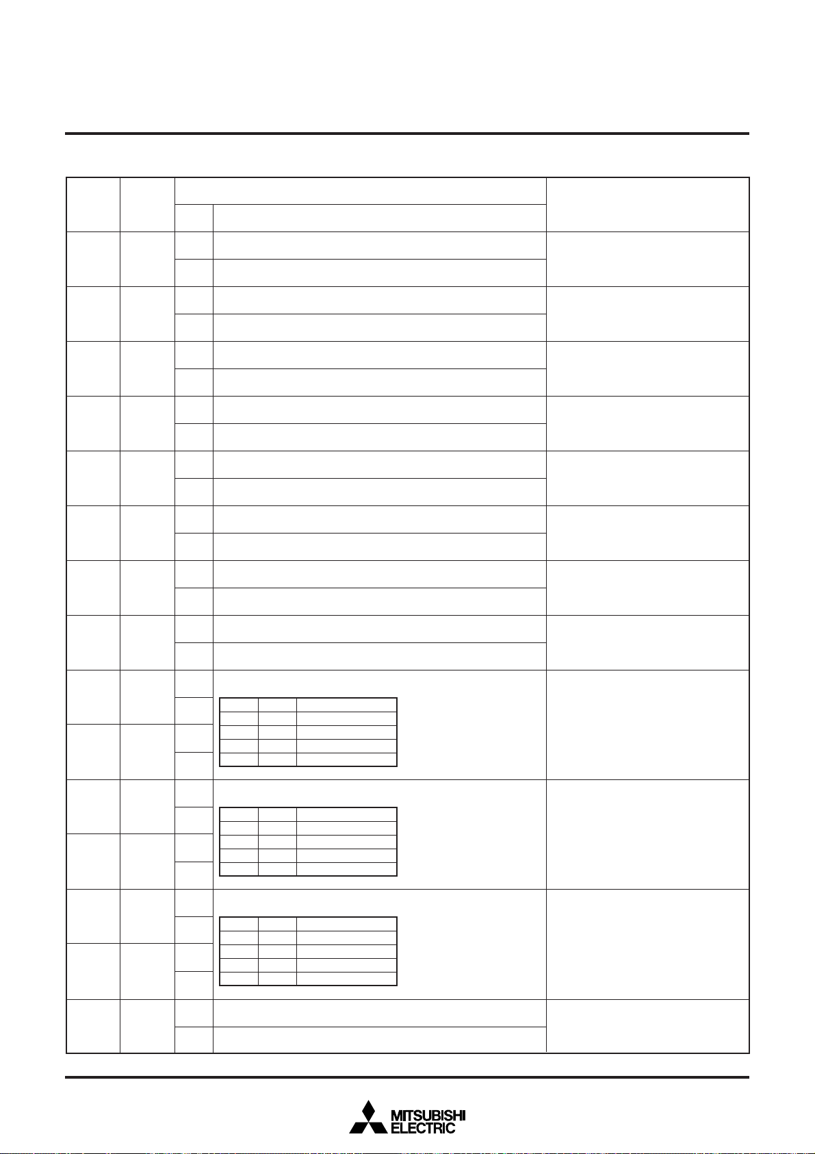
(4) Address 12316
MITSUBISHI MICROCOMPUTERS
M35046-XXXSP/FP
SCREEN CHARACTER and PATTERN DISPLAY CONTROLLERS
RegisterDA
Status
0
0
1
2
3
4
5
6
VP0
(LSB)
VP1
VP2
VP3
VP4
VP5
VP6
If VS is the vertical display start location,
1
VS = H × 2nVPn
0
1023 settings are possible.
1
0
1
0
1
0
1
0
1
0
1
9
Σ
n = 0
H: Cycle with the horizontal synchronizing pulse
H P
T
V
E R
Contents
Function
H O R ( N o t e )
V P
D i s p l a y a r e a
Remarks
The vertical start location is specified
using the 10 bits from VP9 to VP0.
VP9 to VP0 = (00000000002) setting is
forbidden.
Note : In case of B/F register is “0”.
_
0
7
8
9
A
B
C
D
E
VP7
VP8
VP9
(MSB)
TEST0
TEST1
TEST2
TEST3
EXCK1
1
0
1
0
1
0
It should be fixed to “0”.
1
Can not be used.
0
It should be fixed to “0”.
1
Can not be used.
0
It should be fixed to “0”.
1
Can not be used.
0
It should be fixed to “0”.
1
Can not be used.
0
For setting. See Register EXCK0 (address 12016).
1
Sets input mode of external clock (input
from TCK pin).
8

(5) Address 12416
MITSUBISHI MICROCOMPUTERS
M35046-XXXSP/FP
SCREEN CHARACTER and PATTERN DISPLAY CONTROLLERS
RegisterDA
Status
0
0
1
2
3
4
5
6
DSP0
DSP1
DSP2
DSP3
DSP4
DSP5
DSP6
Blanking is in the display mode specified by BLK0 and BLK1. (Note)
1
Blanking is in the display mode specified by except BLK0 and BLK1. (Note)
0
Blanking is in the display mode specified by BLK0 and BLK1. (Note)
1
Blanking is in the display mode specified by except BLK0 and BLK1. (Note)
0
Blanking is in the display mode specified by BLK0 and BLK1. (Note)
1
Blanking is in the display mode specified by except BLK0 and BLK1. (Note)
0
Blanking is in the display mode specified by BLK0 and BLK1. (Note)
1
Blanking is in the display mode specified by except BLK0 and BLK1. (Note)
0
Blanking is in the display mode specified by BLK0 and BLK1. (Note)
1
Blanking is in the display mode specified by except BLK0 and BLK1. (Note)
0
Blanking is in the display mode specified by BLK0 and BLK1. (Note)
1
Blanking is in the display mode specified by except BLK0 and BLK1. (Note)
0
Blanking is in the display mode specified by BLK0 and BLK1. (Note)
1
Blanking is in the display mode specified by except BLK0 and BLK1. (Note)
Contents
Function
Remarks
Sets the display mode of line 1.
Sets the display mode of line 2.
Sets the display mode of line 3.
Sets the display mode of line 4.
Sets the display mode of line 5.
Sets the display mode of line 6.
Sets the display mode of line 7.
0
7
8
9
A
B
C
D
E
Note: Refer to DISPLAY FORM1.
DSP7
1
0
DSP8
1
0
DSP9
1
0
DSP10
1
0
DSP11
1
0
TEST4
1
0
TEST5
1
0
TEST14
1
Blanking is in the display mode specified by BLK0 and BLK1. (Note)
Blanking is in the display mode specified by except BLK0 and BLK1. (Note)
Blanking is in the display mode specified by BLK0 and BLK1. (Note)
Blanking is in the display mode specified by except BLK0 and BLK1. (Note)
Blanking is in the display mode specified by BLK0 and BLK1. (Note)
Blanking is in the display mode specified by except BLK0 and BLK1. (Note)
Blanking is in the display mode specified by BLK0 and BLK1. (Note)
Blanking is in the display mode specified by except BLK0 and BLK1. (Note)
Blanking is in the display mode specified by BLK0 and BLK1. (Note)
Blanking is in the display mode specified by except BLK0 and BLK1. (Note)
It should be fixed to “0”.
Can not be used.
It should be fixed to “0”.
Can not be used.
Can not be used.
It should be fixed to “1”.
Sets the display mode of line 8.
Sets the display mode of line 9.
Sets the display mode of line 10.
Sets the display mode of line 11.
Sets the display mode of line 12.
9
(6) Address 12516
MITSUBISHI MICROCOMPUTERS
M35046-XXXSP/FP
SCREEN CHARACTER and PATTERN DISPLAY CONTROLLERS
RegisterDA
Status
The first line is set by VSZ1L0 and VSZ1L1.
0
0
1
2
3
4
5
6
7
8
9
LIN2
LIN3
LIN4
LIN5
LIN6
LIN7
LIN8
LIN9
V1SZ0
V1SZ1
The second to 12th lines are set by VSZ2L0 and VSZ2L1.
The first line is set by VSZ1H0 and VSZ1H1.
1
The second to 12th lines are set by VSZ2H0 and VSZ2H1.
The first line is set by VSZ1L0 and VSZ1L1.
0
The second to 12th lines are set by VSZ2L0 and VSZ2L1.
The first line is set by VSZ1H0 and VSZ1H1.
1
The second to 12th lines are set by VSZ2H0 and VSZ2H1.
The first line is set by VSZ1L0 and VSZ1L1.
0
The second to 12th lines are set by VSZ2L0 and VSZ2L1.
The first line is set by VSZ1H0 and VSZ1H1.
1
The second to 12th lines are set by VSZ2H0 and VSZ2H1.
The first line is set by VSZ1L0 and VSZ1L1.
0
The second to 12th lines are set by VSZ2L0 and VSZ2L1.
The first line is set by VSZ1H0 and VSZ1H1.
1
The second to 12th lines are set by VSZ2H0 and VSZ2H1.
The first line is set by VSZ1L0 and VSZ1L1.
0
The second to 12th lines are set by VSZ2L0 and VSZ2L1.
The first line is set by VSZ1H0 and VSZ1H1.
1
The second to 12th lines are set by VSZ2H0 and VSZ2H1.
The first line is set by VSZ1L0 and VSZ1L1.
0
The second to 12th lines are set by VSZ2L0 and VSZ2L1.
The first line is set by VSZ1H0 and VSZ1H1.
1
The second to 12th lines are set by VSZ2H0 and VSZ2H1.
The first line is set by VSZ1L0 and VSZ1L1.
0
The second to 12th lines are set by VSZ2L0 and VSZ2L1.
The first line is set by VSZ1H0 and VSZ1H1.
1
The second to 12th lines are set by VSZ2H0 and VSZ2H1.
The first line is set by VSZ1L0 and VSZ1L1.
0
The second to 12th lines are set by VSZ2L0 and VSZ2L1.
The first line is set by VSZ1H0 and VSZ1H1.
1
The second to 12th lines are set by VSZ2H0 and VSZ2H1.
H: Cycle with the horizontal synchronizing pulse
0
V1SZ1
V1SZ0
1
0
1
0
0
1
1
Vertical direction size
0
1
0
1
1H/dot
2H/dot
3H/dot
4H/dot
Function
Character size setting in the vertical
direction for the 2nd line.
Character size setting in the vertical
direction for the 3rd line.
Character size setting in the vertical
direction for the 4th line.
Character size setting in the vertical
direction for the 5th line.
Character size setting in the vertical
direction for the 6th line.
Character size setting in the vertical
direction for the 7th line.
Character size setting in the vertical
direction for the 8th line.
Character size setting in the vertical
direction for the 9th line.
Character size setting in the vertical
direction for the 1st line.
(display monitor 1 to 12 line)
Remarks
Contents
10
H: Cycle with the horizontal synchronizing pulse
A
VSZ1L0
B
VSZ1L1
C
VSZ1H0
D
VSZ1H1
E
TEST10
0
VSZ1L1
1
0
1
H: Cycle with the horizontal synchronizing pulse
0
1
0
1
It should be fixed to “0”.
0
Test mode
1
0
0
1
1
VSZ1H1
0
0
1
1
VSZ1L0
VSZ1H0
Vertical direction size
0
1
0
1
Vertical direction size
0
1
0
1
1H/dot
2H/dot
3H/dot
4H/dot
1H/dot
2H/dot
3H/dot
4H/dot
Character size setting in the vertical
direction (display monitor 1 line) at “0”
state in register LIN2 to LIN17.
Character size setting in the vertical
direction (display monitor 1 line) at “1”
state in register LIN2 to LIN17.
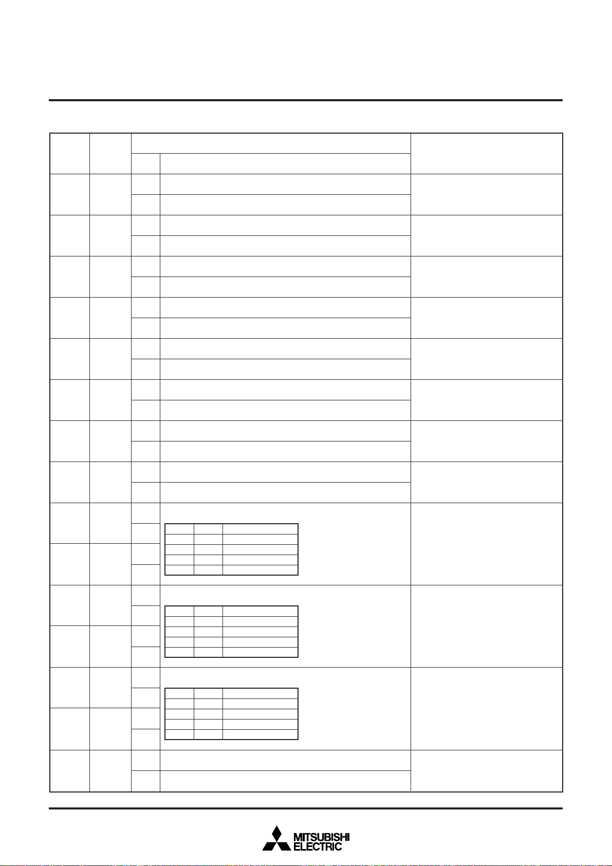
(7) Address 12616
MITSUBISHI MICROCOMPUTERS
M35046-XXXSP/FP
SCREEN CHARACTER and PATTERN DISPLAY CONTROLLERS
RegisterDA
Status
The first line is set by VSZ1L0 and VSZ1L1.
0
0
1
2
3
4
5
6
7
8
9
LIN10
LIN11
LIN12
LIN13
LIN14
LIN15
LIN16
LIN17
V18SZ0
V18SZ1
The second to 12th lines are set by VSZ2L0 and VSZ2L1.
The first line is set by VSZ1H0 and VSZ1H1.
1
The second to 12th lines are set by VSZ2H0 and VSZ2H1.
The first line is set by VSZ1L0 and VSZ1L1.
0
The second to 12th lines are set by VSZ2L0 and VSZ2L1.
The first line is set by VSZ1H0 and VSZ1H1.
1
The second to 12th lines are set by VSZ2H0 and VSZ2H1.
The first line is set by VSZ1L0 and VSZ1L1.
0
The second to 12th lines are set by VSZ2L0 and VSZ2L1.
The first line is set by VSZ1H0 and VSZ1H1.
1
The second to 12th lines are set by VSZ2H0 and VSZ2H1.
The first line is set by VSZ1L0 and VSZ1L1.
0
The second to 12th lines are set by VSZ2L0 and VSZ2L1.
The first line is set by VSZ1H0 and VSZ1H1.
1
The second to 12th lines are set by VSZ2H0 and VSZ2H1.
The first line is set by VSZ1L0 and VSZ1L1.
0
The second to 12th lines are set by VSZ2L0 and VSZ2L1.
The first line is set by VSZ1H0 and VSZ1H1.
1
The second to 12th lines are set by VSZ2H0 and VSZ2H1.
The first line is set by VSZ1L0 and VSZ1L1.
0
The second to 12th lines are set by VSZ2L0 and VSZ2L1.
The first line is set by VSZ1H0 and VSZ1H1.
1
The second to 12th lines are set by VSZ2H0 and VSZ2H1.
The first line is set by VSZ1L0 and VSZ1L1.
0
The second to 12th lines are set by VSZ2L0 and VSZ2L1.
The first line is set by VSZ1H0 and VSZ1H1.
1
The second to 12th lines are set by VSZ2H0 and VSZ2H1.
The first line is set by VSZ1L0 and VSZ1L1.
0
The second to 12th lines are set by VSZ2L0 and VSZ2L1.
The first line is set by VSZ1H0 and VSZ1H1.
1
The second to 12th lines are set by VSZ2H0 and VSZ2H1.
0
H: Cycle with the horizontal synchronizing pulse
V18SZ1
1
0
1
V18SZ0
0
0
1
1
Vertical direction size
0
1
0
1
1H/dot
2H/dot
3H/dot
4H/dot
Function
Character size setting in the vertical
direction for the 10th line.
Character size setting in the vertical
direction for the 11th line.
Character size setting in the vertical
direction for the 12th line.
Character size setting in the vertical
direction for the 13th line.
Character size setting in the vertical
direction for the 14th line.
Character size setting in the vertical
direction for the 15th line.
Character size setting in the vertical
direction for the 16th line.
Character size setting in the vertical
direction for the 17th line.
Character size setting in the vertical
direction for the 18th line.
(display monitor 1 to 12 line)
Remarks
Contents
0
H: Cycle with the horizontal synchronizing pulse
A
VSZ2L0
B
VSZ2L1
C
VSZ2H0
D
VSZ2H1
E
TEST11
VSZ2L1
1
0
1
0
H: Cycle with the horizontal synchronizing pulse
1
0
1
0
It should be fixed to “0”.
1
Test mode
0
0
1
1
VSZ2H1
0
0
1
1
VSZ2L0
VSZ2H0
Vertical direction size
0
1
0
1
Vertical direction size
0
1
0
1
1H/dot
2H/dot
3H/dot
4H/dot
1H/dot
2H/dot
3H/dot
4H/dot
Character size setting in the vertical
direction (display monitor for 2 to 12
line) at “0” state in register LIN2 to
LIN17.
Character size setting in the vertical
direction (display monitor for 2 to 12
line) at “1” state in register LIN2 to
LIN17.
11
 Loading...