

Page 1
2008
CAUTION
Before servicing this chassis, it is important that the service person reads the “SAFETY PRECAUTIONS” and “PRODUCT
SAFETY NOTICE” in this service manual.
Copyright © 2008 Mitsubishi Electric Corporation All Rights Reserved.
MODEL
XL6500LU/
XL6500U
This model is RoHS-compliant.
Provide servicing referring to “NOTES
FOR SERVICING RoHS-COMPLIANT
PRODUCTS” described in the service
manual.
Pb Solder, Pb Joints, Pb PCA
This product uses lead-free solder
on the circuit boards. For repairing
circuit boards, see "Precautions for
resoldering" in this Service Manual.
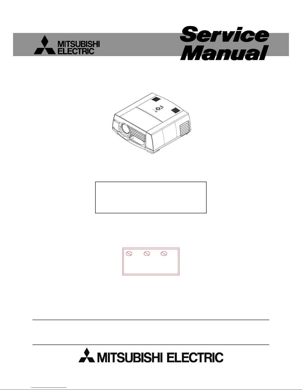
LCD PROJECTOR
LC62 CHASSIS
Page 2
- 2 -
NOTES FOR SERVICING RoHS-COMPLIANT PRODUCTS
Follow the notes and instructions below when servicing RoHS-compliant
products.
1. For RoHS-compliant products, be sure to use RoHS-compliant service parts.
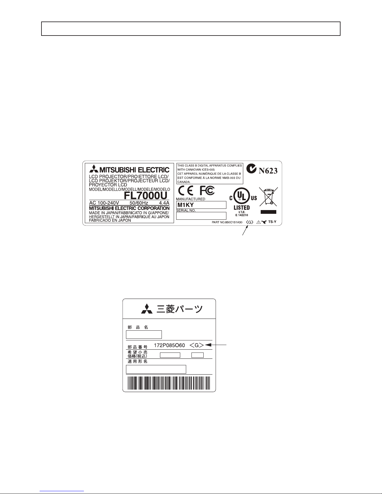
2. Check the presence of <G> marking on the rating plate to distinguish RoHScompliant product from non-RoHS-compliant product.
<G> marking
With <G> marking: RoHS-compliant product
Without <G> marking: Non-RoHS-compliant product
<Sample>
3. Labels of RoHS-compliant service parts bear <G> marking for identifi cation purpose.
<Sample>
4. Don’t use non-RoHS-compliant parts with RoHS-compliant products.
5. Service parts for RoHS-compliant products are listed in the parts catalog contained
in the service manual.
Parts Name
Model Name
Parts No.
E05R
Mark position
Mark position
Page 3

- 3 -
SPECIFICATIONS
• Rated Voltage
•
Power Consumption
•
Display Technology
• Projection Lens
•
Light Source Lamp
• Image Size
(projection distance)
•
Maximum Resolution
• S-Video Input
• Video Input
• Component Video Input
• Analog Input
•
Digital Input (DVI)
• Audio Input
• Speaker
• Control Terminal/
Others
• Dimensions
(not including protrusion)
• Weight
•
Operating temperatures
: AC 100 to 240V ; 50/60Hz,
: 4.4A
:
1.3 inch LCD panel ; 3 pieces (for R,G,B)
:
Pixels ; 1,024 × 768 = 786,432 pixels
Total 2,359,296 pixels
:
Active pixel rate ; 99.99 % or more (each panel)
: F 1.8 - 2.1 f = 51 - 64 mm[XL6500U]
: 275 W
:60 to 300 inch[XL6500U]
(projection distance ; 2.3 to 11.6 m)
:
Computer signal
Maximum resolution ; 1,600 × 1,200 dots(Compressed
)
Panel resolution ; 1,024 × 768 dots
:Video signal
NTSC/PAL/SECAM/4.43NTSC/PAL-M/PAL-N/PAL-60
:Component signal
480i,480p,576i,576p,720p,1080i,1080p
Panel resolution ; 1,024 × 768 dots
:
Luminance signal ; 1.0 V(p-p) 75Ω (negative sync)
Chrominance signals ; 0.286 V(p-p) 75Ω (burst signal)
: 1.0 V(p-p) 75 Ω (negative sync)
: YC
BCR
;
Y ; 1.0 V(p-p) 75 Ω (negative sync)
C
BCR ;
0.7 V(p-p) 75 Ω
: RGB ;
0.7 V(p-p) 75 Ω (negative sync)
: YCBCR ;
Y ; 1.0 V(p-p) (negative sync)
C
BCR ;
0.7 V(p-p)
: HD/CS ;
TTL level (negative or positive polarity)
: VD ;
TTL level (negative or positive polarity)
:
DVI-D interface (TMDS single link) with HDCP
: 350 mVrms, 10 k
Ω or more
: 10 W mono Round type ø 4.5 cm × 1
: RS-232C (D-SUB 9 pin),USB,
LAN (RJ-45),REMOTE IN/OUT
: 371 (W) × 207 (H) × 434 (D) mm
(projector only)
443 (W) × 207 (H) × 434 (D) mm
(including the terminal cover)
: 9.8 kg (projector only)
: 10.5 kg (including the terminal cover)
: + 41 °F (+ 5°C) to 104 °F (+ 40 °C)
• Weight and dimensions shown are approximate.
• Design and specifi cations are subject to change without notice.
Page 4

- 4 -
CONTENTS
– FILE “COVERPGE” –
NOTES FOR SERVICING RoHS-COMPLIANT PRODUCTS ............................................................................... 2
SPECIFICATIONS ................................................................................................................................................. 3
CONTENTS ........................................................................................................................................................... 4
– FILE “EXPOSED” –
TRADE MARK, REGISTERED TRADEMARK ...................................................................................................... 1
PRODUCT SAFETY NOTICE ............................................................................................................................... 1
SAFETY PRECAUTIONS ...................................................................................................................................... 2
PRECAUTIONS FOR RESOLDERING ................................................................................................................. 3
PCB LOCATION .................................................................................................................................................... 4
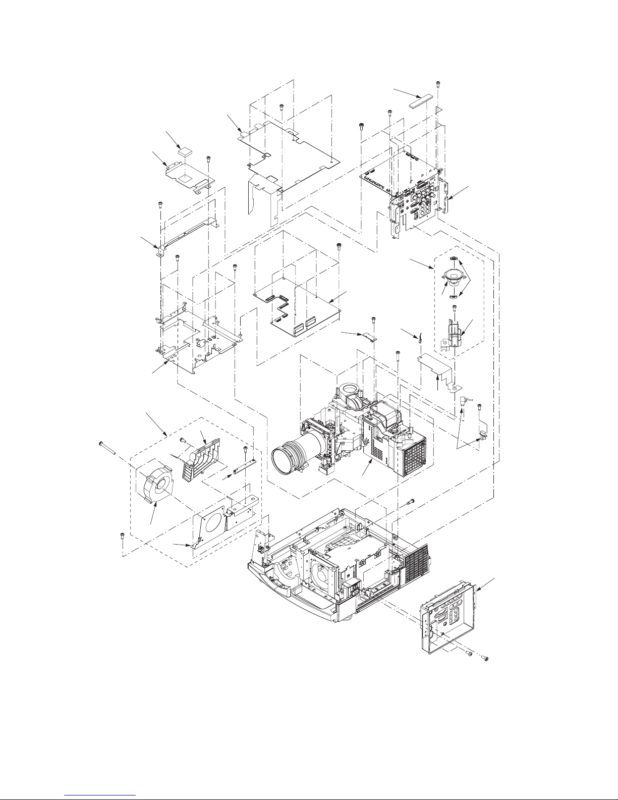
EXPOSED VIEW ................................................................................................................................................... 6
LVP ASSY ...................................................................................................................... .................................. 6
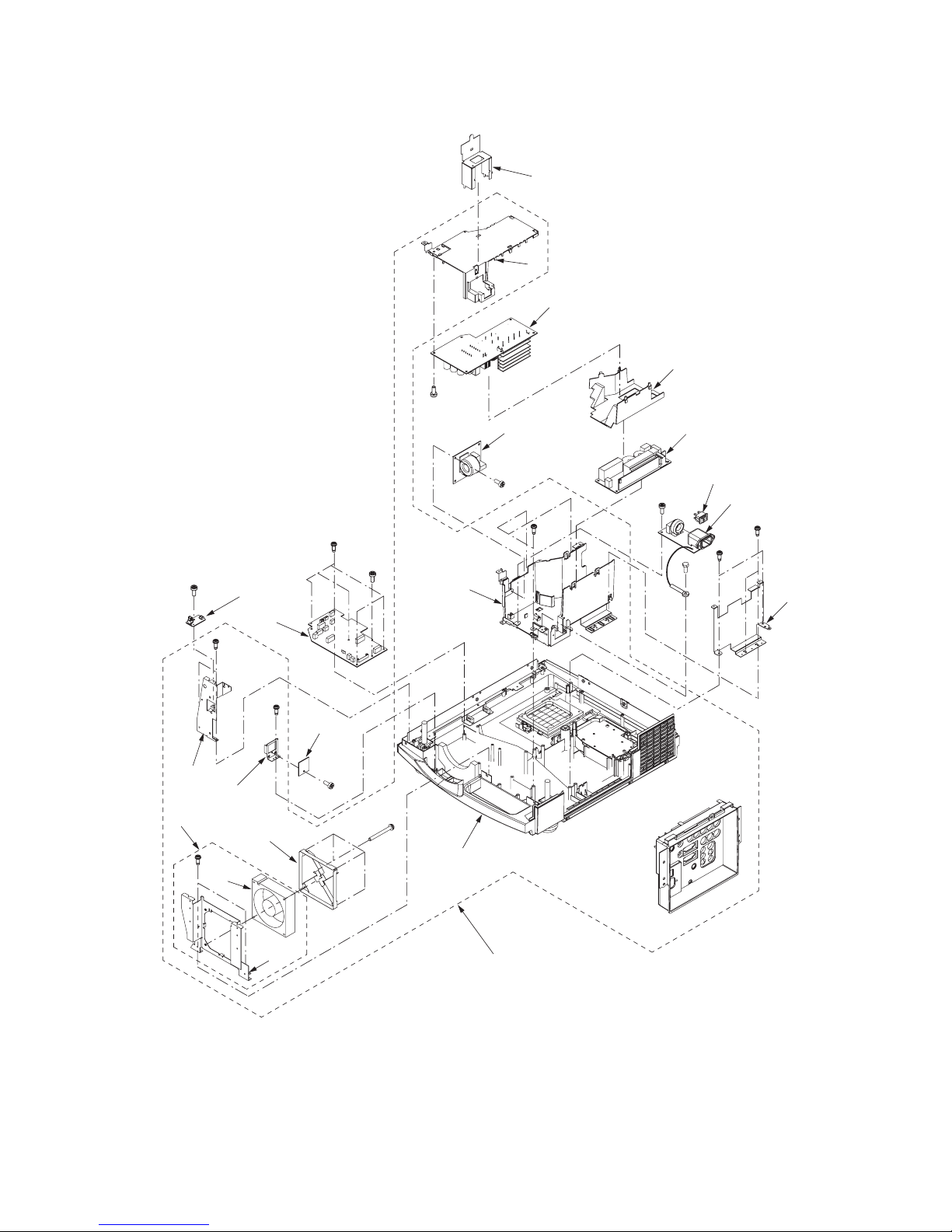
Chassis 1 ASSY ............................................................................................................................................... 8
Chassis 2 ASSY ............................................................................................................................................... 10
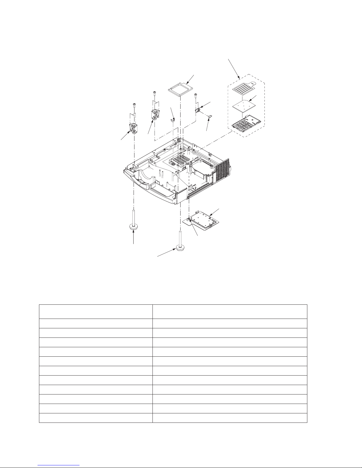
Bottom case unit .............................................................................................................................................. 12
T erminal ASSY ................................................................................................................................................. 13
Optical unit 1 .................................................................................................................................................... 14
Optical unit 2 .................................................................................................................................................... 16
POSITION ADJUSTMENT OF MULTI LENS A ..................................................................................................... 17
DISASSEMBLY ................................................................................................................... .................................. 18
1.Removal of the terminal cover ASSY ............................................................................................................ 18
2.Removal of the BOO PCB ASSY and BOO SUB PCB ASSY ....................................................................... 18
3.Removal of the lens unit and zoom focus motor ........................................................................................... 19
4.Removal of the top case unit and KEY PCB ASSY ...................................................................................... 20
5.Removal of the IRF PCB ASSY .................................................................................................................... 21
6.Removal of the MOTOR PCB ASSY ............................................................................................................. 21
7.Removal of the IRR PCB ASSY .................................................................................................................... 21
8.Removal of the speaker ................................................................................................................................ 22
9.Removal of the power fan ............................................................................................................................. 22
10.Removal of the MAIN PCB ASSY ............................................................................................................... 23
11.Removal of the TERMINAL PCB ASSY ...................................................................................................... 23
12.Removal of the DRIVE PCB ASSY and LCD block .................................................................................... 24
13.Removal of the drive fan ............................................................................................................................. 25
14.Removal of the PBS fan ............................................................................................................................. 25
15.Removal of the optical unit ......................................................................................................................... 26
16.Removal of the POWER PCB ASSY .......................................................................................................... 27
17.Removal of the lamp power unit ................................................................................................................. 28
18.Removal of the FILTER PCB ASSY and INLET PCB ASSY ....................................................................... 28
19.Removal of the POWER SUB PCB ASSY .................................................................................................. 29
20.Removal of the lamp fan ............................................................................................................................. 30
21.Removal of the LCD fan ............................................................................................................................. 30
22.Removal of the exhaust fan ........................................................................................................................ 31
23.Removal of the lens shift motor .................................................................................................................. 31
24.Removal of the lamp box ............................................................................................................................ 32
LAMP REPLACEMENT ......................................................................................................................................... 32
LEAD DRESS ........................................................................................................................................................ 33
PACKING ............................................................................................................................................................... 38
– FILE “MAINTENA” –
LAMP REPLACEMENT ......................................................................................................................................... 1
MAINTENANCE .................................................................................................................................................... 3
HOW TO USE THE LAMP JIG .............................................................................................................................. 4
DUST ON LCD PANEL .......................................................................................................................................... 5
RESET OF THE THERMAL PROTECTOR ........................................................................................................... 5
SERVICE COMMANDS ........................................................................................................................................ 6
Display the operation status screen .................................................................................................................
6
Reset to the factory settings ............................................................................................................................ 6
Reset the lamp operating time ......................................................................................................................... 6
LIFE TIME OF THE CONSUMABLE PARTS ........................................................................................................ 7
FUNCTION MENU(SETTING MENU ONLY FOR SERVICE) ............................................................................... 8
REPLACEMENT OF THE MAIN PCB ASSY ......................................................................................................... 9
REPLACEMENT OF THE TERMINAL PCB ASSY ................................................................................................ 10
GAMMA ADJUSTMENT(WHITE BALANCE ADJUSTMENT) ............................................................................... 10
UNIFORMITY DATA TRANSFER .......................................................................................................................... 12
COLOR UNIFORMITY ADJUSTMENT ................................................................................................................. 13
DOWNLOAD OF THE FIRMWARE ....................................................................................................................... 15
CRITERIA OF THE DEFECT PIXEL ON THE LCD PANEL(FOR REFERENCE PURPOSE) .............................. 16
ABOUT LASER BEAM .......................................................................................................................................... 18
Page 5

- 5 -
– FILE “ELCTADJ” –
ELECTRICAL ADJUSTMENTS ............................................................................................................................. 1
Necessary Equipment and Connecting ........................................................................................................... 1
Test Signal ....................................................................................................................................................... 1
Adjustment with Microsoft
®
Windows® 95/98/Me/XP Operating System ......................................................... 2
Adjustment Procedures ................................................................................................................................... 3
– FILE “DIAGNO” –
DIAGNOSIS INFORMATION ................................................................................................................................. 1
DIAGNOSTIC SOFTWARE,TO READ WARNING HISTORY(PCGC8 Ver.2) ....................................................... 3
SPECIFICATION OF RGB SIGNALS IN EACH COMPUTER MODE OF THE PROJECTOR .............................. 5
– FILE “DIAGFLOW” –
DIAGNOSIS FLOW CHART .................................................................................................................................. 1
Image system .................................................................................................................................................. 1
Power source system 1 ................................................................................................................................... 2
Power source system 2 ................................................................................................................................... 3
Power source system 3 ................................................................................................................................... 4
– FILE “PCCONTRL” –
Controling the prijector using a personal computer ............................................................................................... 1
– FILE “PARTSLST” –
PARTS LIST .......................................................................................................................................................... 1
PCB LOCATION .............................................................................................................................................. 2
EXPOSED VIEW ............................................................................................................................................. 3
LVP ASSY .................................................................................................................................................. 3
Chassis 1 ASSY ......................................................................................................................................... 4
Chassis 2 ASSY ......................................................................................................................................... 5
Bottom case unit ........................................................................................................................................ 6
Terminal ASSY ........................................................................................................................................... 6
Optical unit 1 .............................................................................................................................................. 7
Optical unit 2 .............................................................................................................................................. 8
PACKING ....................................................................................................................... .................................. 9
ELECTRICAL PARTS AND OTHERS .............................................................................................................. 10
– FILE “SCHEMATC” –
IC BLOCK DIAGRAMS
SCHEMATIC DIAGRAMS
PRINTED CIRCUIT BOARD PARTS LAYOUT
Page 6
- 1 -
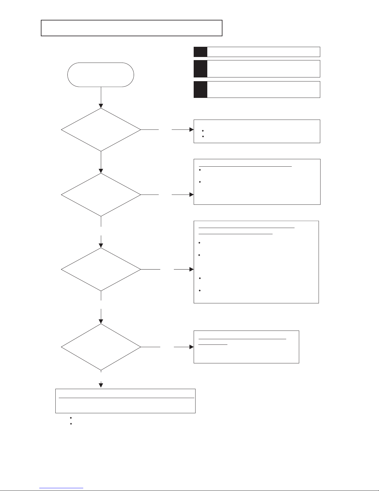
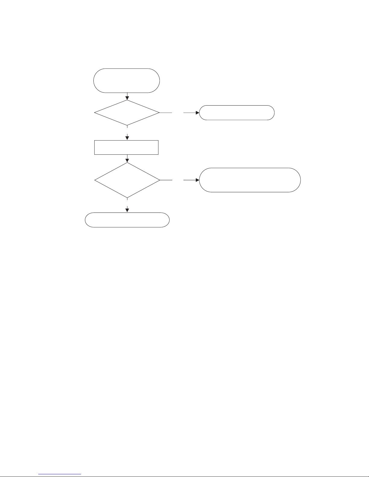
DIAGNOSIS FLOW CHART
Image system
The terminal shield is used as GND when the terminal voltages and the waveforms are checked.
When replacing the PCB or the optical unit, follow the instructions in the service manual.
Is the lamp lit?
Is the indication of LEDs normal after power-on?
(POWER : Green, STATUS : Green)
Is the proper video signal supplied?
Is the image projected correctly?
NO
YES
NO
YES
NO
YES
Malfunction of the PCB-MAIN or the PCB-DRIVE.
Check the voltage waveforms of the SV, and SW
connectors on the PCB-MAIN respectively.
Check the voltage waveforms of the DR, DG,and DB
connectors on the PCB-DRIVE respectively.
*
Malfunction of the LCD panel when the
above-mentioned voltage waveforms are OK.
Malfunction of the analog/digital circuit around the input
terminal of the computer.
[Analog input]
(PCB-TERMINAL/PCB-MAIN)
Check the video signal circuits around J600, J603,
IC610 (PCB-TERMINAL), and IC6A0 (PCB-MAIN).
Check the sync signal circuits around J600, J603,
IC551, IC552, IC561 (PCB-TERMINAL), and IC6A0
(PCB-MAIN).
[DVI-D input]
Check the video signal circuits around J6P0, and
IC6A0.
Check the DDC interface circuits around J6P0, IC6M0,
and IC6C5.
Malfunction of the circuit around the video
input terminal.
Check the video signal circuits around J210,
J211, IC230, IC231 (PCB-TERMINAL), and
IC2A0 (PCB-MAIN).
A malfunction has occurred in the digital signal processing circuit.
Check the digital signal circuit around IC440.
(SDRAM IC400, IC401, IC402, IC403)
Images are not
projected properly.
Is the menu projected
normally?
NO
Are the full-white,
full-black, monochrome
R, G, and B test signals
projected normally?
Are images from
the computer
projected normally?
Are video images
projected normally?
!
!
!
Malfunction of the PCB-DRIVE.
Are the DR, DG, and DB connectors inserted properly?
Is the voltage at the DP connector OK?
Page 7
- 2 -
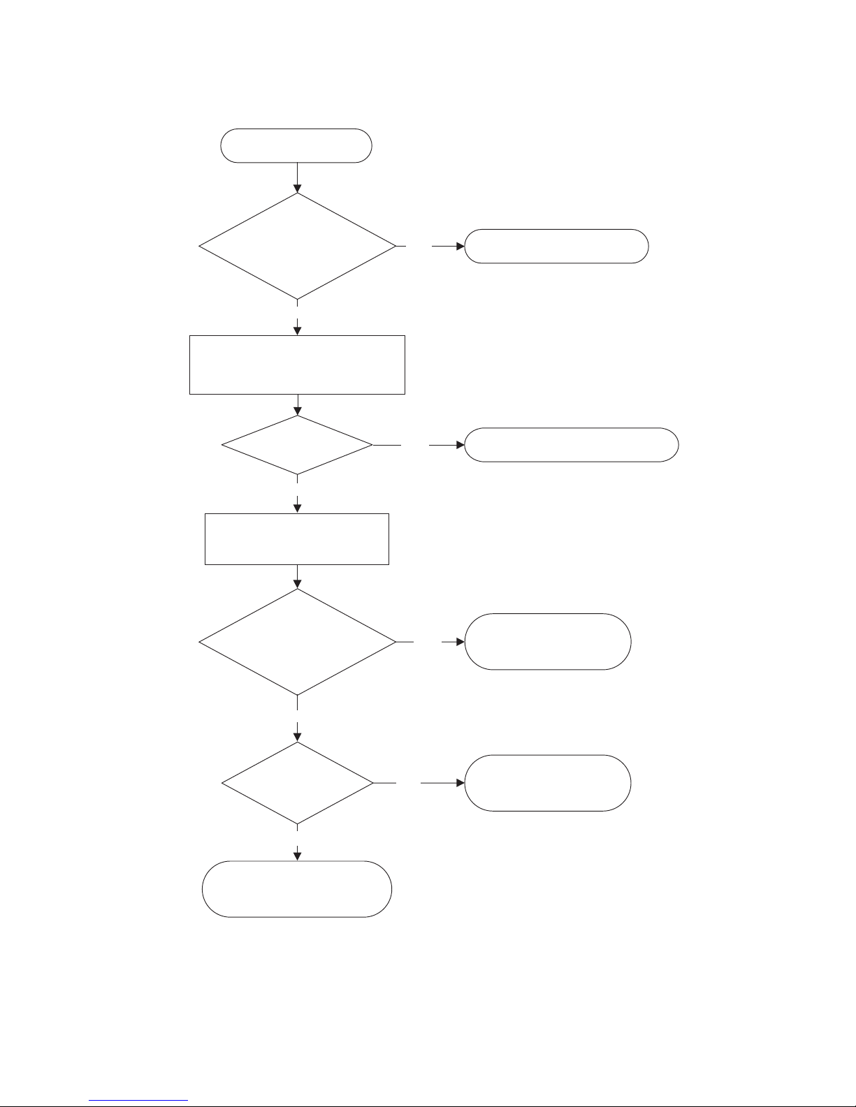
Power source system 1
Has the FUSE
(F9F1) blown?
YES
NO
Replace the lead wire.
Malfunction of the MAIN PCB ASSY
or KEY PCB ASSY.
Malfunction of the MAIN PCB ASSY.
Malfunction of the PREAMP PCB ASSY or the KEY PCB ASSY.
YES
NO
NO
YES
NO
YES
LED doesn't illuminate.
Check the STBY5.
YES
The projector does not
enter the stand-by mode.
Check for any failure on the POWER PCB ASSY,
then replace the parts.
(Check especially D900, Q900, Q901, Q902,
Q905, IC9M0 and IC900.)
Is the lead wire
PB-RB or RD-SD
broken?
Is the pin No. 3
of the SD
connector 5 V?
Remove the
SD connector
from the MAIN
PCB ASSY .
Is the pin No. 3
of the RD
connector 5 V?
Check the circuits around IC950,
IC951, and PC950, and replace them,
if necessary. (Especially check Z952. )
INLET PCB ASSY
MAIN PCB ASSY
POWER PCB ASSY
Replace the
MAIN PCB ASSY and
check if the product enters
the stand-by
mode.
NO
The terminal shield can be used as GND when the terminal voltages and the waveforms on the
secondary side are checked.
(Do not use a heat dissipation board as GND.)
Is the PP,PF-RF
or RD-SD connectors
inserted properly?
NO
YES
Insert the connectors properly.
Page 8
- 3 -
Power source system 2
NO
YES
NO
The terminal shield can be used as GND when the terminal voltages and the waveforms on the
secondary side are checked.
(Do not use a heat dissipation board as GND.)
Connect the lead wire correctly,
or replace it.
When diagnosed as a
STBY5 power error.
Is the RD-SD
lead wire OK?
Remove the SD connector
from the MAIN PCB ASSY.
Is the pin No. 6 of
the RD connector
-6 V or less?
YES
Malfunction of the MAIN
PCB ASSY
.
Check the circuits around D983 (on the
POWER
PCB ASSY
), and replace it,
if necessary.
Page 9
- 4 -
Power source system 3
NO
YES
NO
YES
YES
NO
YES
Malfunction of the the MAIN PCB ASSY.
Connect the lead wires correctry,
or replace them.
The lamp does not light.
Does the lamp light?
NO
Remove the MAIN PCB ASSY and
connect the
LAMP JIG
.
Turn on [FAN-ON], and [LAMP-ON] of the
LAMP JIG
.
Remove the RE-CN1 lead wire and
turn on
[FAN-ON]
of the LAMP JIG.
Is the voltage between
the pins No. 1 and No.
3 of the RE connector
370 V?
Malfunction of the LAMP
POWER UNIT.
Check the circuit around
Z900, IC900, and PC901.
Is the voltage of the
pin No. 10 of IC9M0
17.5 V or more?
Malfunction of the PFC circuit.
Check the circuits around
IC9M0, Q900, Q901, and Q902.
POWER PCB ASSY
Is the lead wire or
connector between the
POWER PCB ASSY and
LAMP POWER UNIT
OK?
POWER PCB ASSY
The terminal shield can be used as GND when the terminal voltages and the waveforms on the
secondary side are checked.
(Do not use a heat dissipation board as GND.)
When measuring the voltage on the primary side, use the negative (-) terminal of C903 as GND.
Page 10
- 1 -
DIAGNOSIS INFORMATION
Outline of self-diagnosis function
This projector is provided with the self-diagnosis function. In case of any failure, the LED at the top of the projector will indicate
the failure. There are two ways for diagnosis.
1. Connect a personal computer to the projector. Then, input [00~CHK] from the hyper-terminal window of the personal computer during stand-by.
2. Connect a personal computer and click the “diagnosis” button of PCGC, the diagnostic software to read the warning history.
Note: Diagnosis can be also carried out by turning on the main power and then turning on the power of the operation panel.
However, as the diagnosis items are different and it may cause a secondary failure, carry out the diagnosis in either of
the above-mentioned ways in most cases.
Diagnosis result indication
LED indication and failures are described in the following table. LED can be reset “automatically” or “by turning on/off of the
main power” after the failure is corrected.
LED Error Indication List
--- : LED off Orange : Both Red and Green light
Preferen-
tial order
LED Indication
Symptom Failure
Check Point
Reset
POWER STATUS PCB Reference
1 --- ---
STBY5 is not
supplied.
AC system (Primary power source)
failure
INLET F9F1
Unplug and plug
the power cord.
Secondary power source failure POWER
SD connector 3pin
(STBY5) , Z972
Unplug and plug
the power cord.
STBY5 is
supplied
LED failure MAIN D7R0
Unplug and plug
the power cord.
2
Red / green
alternately
--- No power-on
Lamp cover open MAIN
SL connector
LAMP COVER
Auto
Filter cover open MAIN
SL connector
Filter cover
Auto
3
Red / green
alternately
red
flash
No power-on
Cooling fan (exhaust) stopped MAIN SX connector
Unplug and plug
the power cord.
red
flash 2
Cooling fan (lamp) stopped
POWER
SUB
NR connector
Unplug and plug
the power cord.
red
flash 3
Cooling fan (power) stopped
POWER
SUB
NA connector
Unplug and plug
the power cord.
red
flash 4
Cooling fan (PBS) stopped
POWER
SUB
NB connector
Unplug and plug
the power cord.
red
flash 5
Cooling fan (intake) stopped
POWER
SUB
NK connector
Unplug and plug
the power cord.
red
flash 6
Cooling fan (drive) stopped
POWER
SUB
ND connector
Unplug and plug
the power cord.
4
Red / green
alternately
Green
No power-on
I2C bus failure of E2PROM MAIN IC445, SCL0, SDA0
Unplug and plug
the power cord
Green
flash
I
2
C bus failure of GPIOO MAIN IC754, SCL0, SDA0
Unplug and plug
the power cord
Green
flash 6
I
2
C bus failure of WatchDog MAIN IC444, SCL0, SDA0
Unplug and plug
the power cord
5
Red / green
alternately
Orange No power-on NR8R power failure
POWER,
MAIN
SD connector 2 pin
(NR8R)
Unplug and plug
the power cord
6
Red / green
alternately
Orange
flash
No power-on Disconnected thermister MAIN SZ connector
Unplug and plug
the power cord
7 Red Red No power-on
Power-on is prohibited because of
the end of the lamp life.
(2000 hours or more)
Replace the lamp and reset the lamp
operating time. (Press and hold the
Power, ,
and buttons on the pro-
jector together for 3 seconds.)
Manual
Page 11
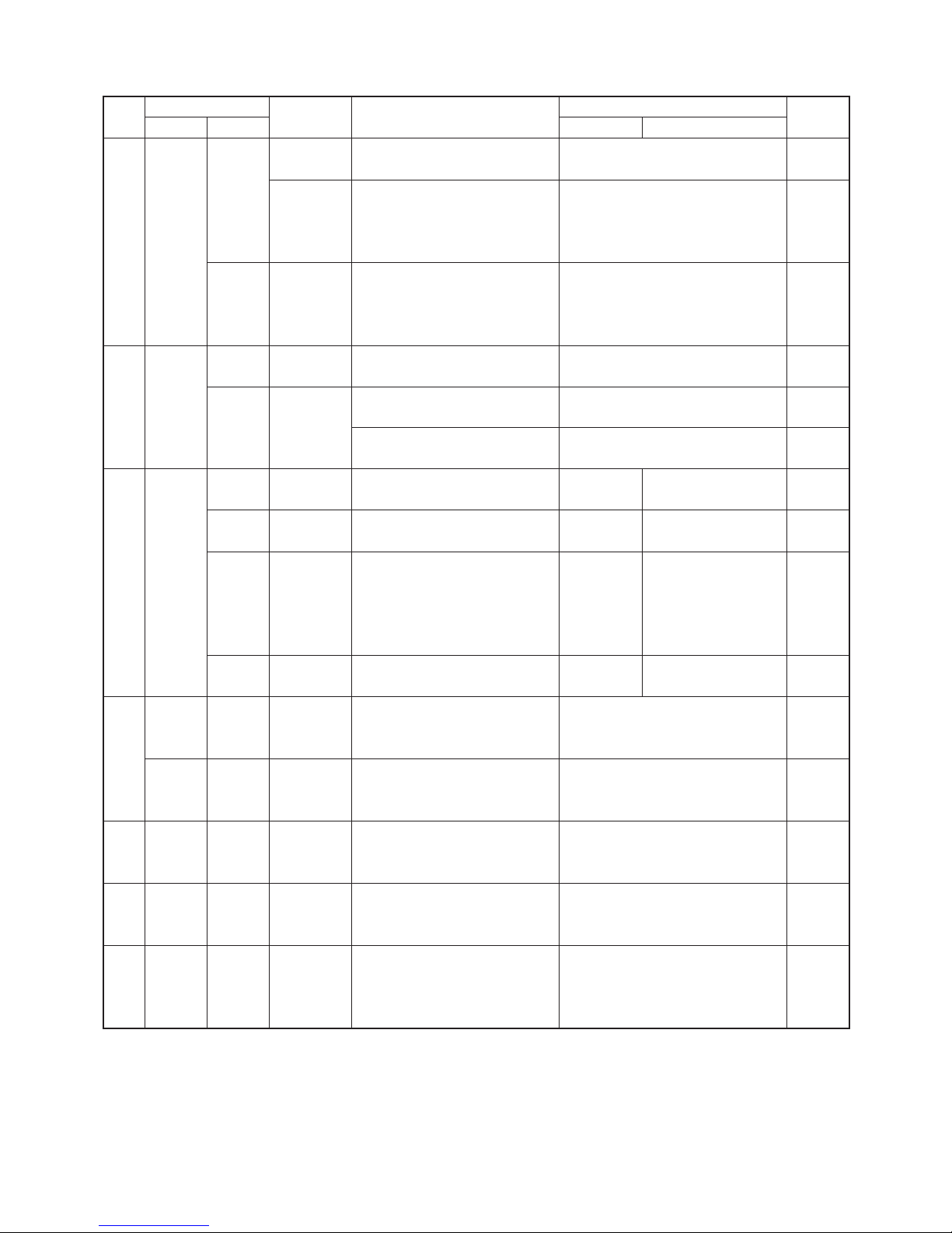
- 2 -
Preferen-
tial order
LED Indication
Symptom Failure
Check Point
Reset
POWER STATUS PCB Reference
8 Red
Orange
flash5
No power-on
High temperature of the intake air
(outside air)
Temperature around the top of the air
inlet fan
Auto
No power-on
after poweroff during
power-on
High temperature of the intake air
(outside air)
Temperature around the top of the air
inlet fan
Auto
Orange
flash 3
No power-on
after poweroff during
power-on
High temperature around the lamp
Temperature around the top of the
lamp
Auto
9 Red
Green
flash
No power-on
for one minute
Lamp fails to illuminate. Auto
Green
flash2
No poweron for one
minute
Lamp goes out. Auto
Damaged lamp
Damaged lamp
Manual
10
Red/
Green al-
ternately
Green
flash 3
RGB signal
isn't displayed.
I2C bus failure of A/D MAIN IC6A0, SCL1, SDA1 Auto
Green
flash 4
VIDEO signal
isn't displayed.
I2C bus failure of DECODER MAIN IC2A0, SCL1, SDA1 Auto
Green
flash 5
VIDEO signal isn't displayed.
I
2
C bus failure of Uniformity Cor-
rection IC
DRIVE
IC4W3,
IC801-IC802,
IC8A1-IC8A2,
IC8M1-IC8M2,
SCL2(HSCL1),SDA2(HSDA1)
Auto
Green
flash 7
VIDEO signal
isn't displayed.
I2C bus failure of AUDIO TERMINAL IC320,AUSDA,AUSCL Auto
11
Red
Red
flash
Warning
indicated by the
LED during stby.
The end of the lamp life is near.
(1500 to 2000h.)
Manual
Green
Red/
Green al-
ternately
Warning indicated
by the LED during
power-on.
The end of the lamp life is near.
(1500 to 2000h.)
Manual
12 Green
Green flash
(cycle : 1s)
No power-off
for one minute
after power-on
For protect the lamp, no power-off
for one minute after power-on
Auto
13 Red
Green
flash
(cycle : 1s)
No poweron for one
minute
Power-on is prohibited during the
lamp cooling time after power-off.
Auto
14 Red
Green
flash
(cycle : 2s)
Displayed for 60
- 80 sec after
power-off. Power
on is possible
After power-off, power-on is possible during the lamp cooling time,
but only FAN rotates.
Auto
Page 12
- 3 -
DIAGNOSTIC SOFTWARE, TO READ WARNING HISTORY (PCGC8 Ver.2)
*Pcgc8 Ver.2 is upwardly compatible with Pcgc8 Ver.1.
1. Preparation
PCGC8 supports Microsoft® Windows® 95/98/Me/XP. Use a
PC with Windows
®
95/98/Me/XP installed.
1. Copy the folder named “Pcgc8.2 (English)”.
2. Connect the PC with the projector by RS-232C cable (service component).
3. Double click “Pcgc8e.exe” in the folder named “Pcgc8.2
(English)” for starting the program.
2. Operation
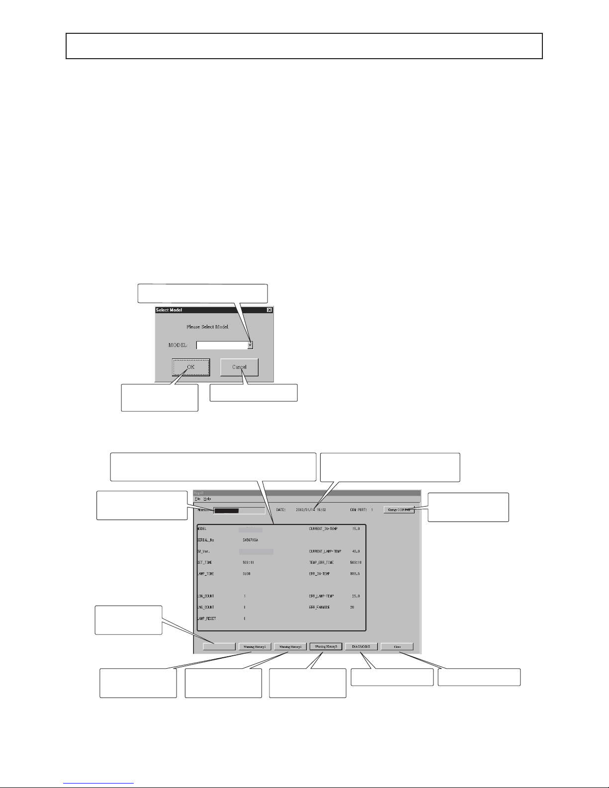
(1) Model name selection dialog window
Starting Pcgc8 displays the model name selection dialog
window. Select the model name you want to use and press
the [OK] button to display the main dialog window. Press the
[Cancel] button to exit the application.
(2) Main dialog window
1. The main dialog window displays the information stored
in the projector (model name, serial No., software version,
etc.) and the service menu information. Information displayed in this window depends on the selected models.
2. Some PCs may not be able to connect to the right COM
port. In such cases, press the Change COM PORT button
to switch the COM port. Refer to (4) Switching the COM
port.
3. Press any of the [Warning History 1], [Warning History 2],
or [Warning History 3] button to display the warning dialog
window containing the detailed error data.
4. Press the [DIAGNOSIS] button to start self-diagnosis.
(Not available during power on and when an error occurs.)
Warning Status : Present abnormal state will be displayed
.After repair, this information will disappear.
Warning History1 : The latest warning history data are stored
in the Warning History 1. The data remain
after the error is corrected.
Warning History 2 : The second oldest warning history data
are stored in the Warning History 2.
Warning History 3 : The oldest warning history data are stored
in the Warning History 3.
Note: When the power is turned off because of any error,
the warning history data are saved. Or, only when
an error occurs during power on or when an error is
detected during self-diagnosis (or immediately after
pressing the DIAGNOSIS button), the warning history data are saved. (The warning history data aren’
t saved when the stand-by power fails during the
stand-by mode. In this case, LED warning indication
will appear. Check the error data by the warning status.)
Goes to the main
dialog window.
Exits this application.
Click and select a model name .
FL7000U
Exits the application.Starts self-diagnosis.
Displays the
Warning History 3.
Displays the
Warning History 2.
Displays the
Warning History 1.
Displays the information about the connected device.
The contents depend on the selected model.
Displays the current date and time
when the error is corrected.
Switches the COM
port.
Displays the
Warning Status
Warning Status
FL7000U
Displays the selected
model name
XL6500U
ver1.0 XL6500
Model name selection dialog window
Main dialogue window
The information to
be displayed varies depending on
the model.
When use XL6500U
or XL6500LU, select
FL7000U.
Page 13
- 4 -
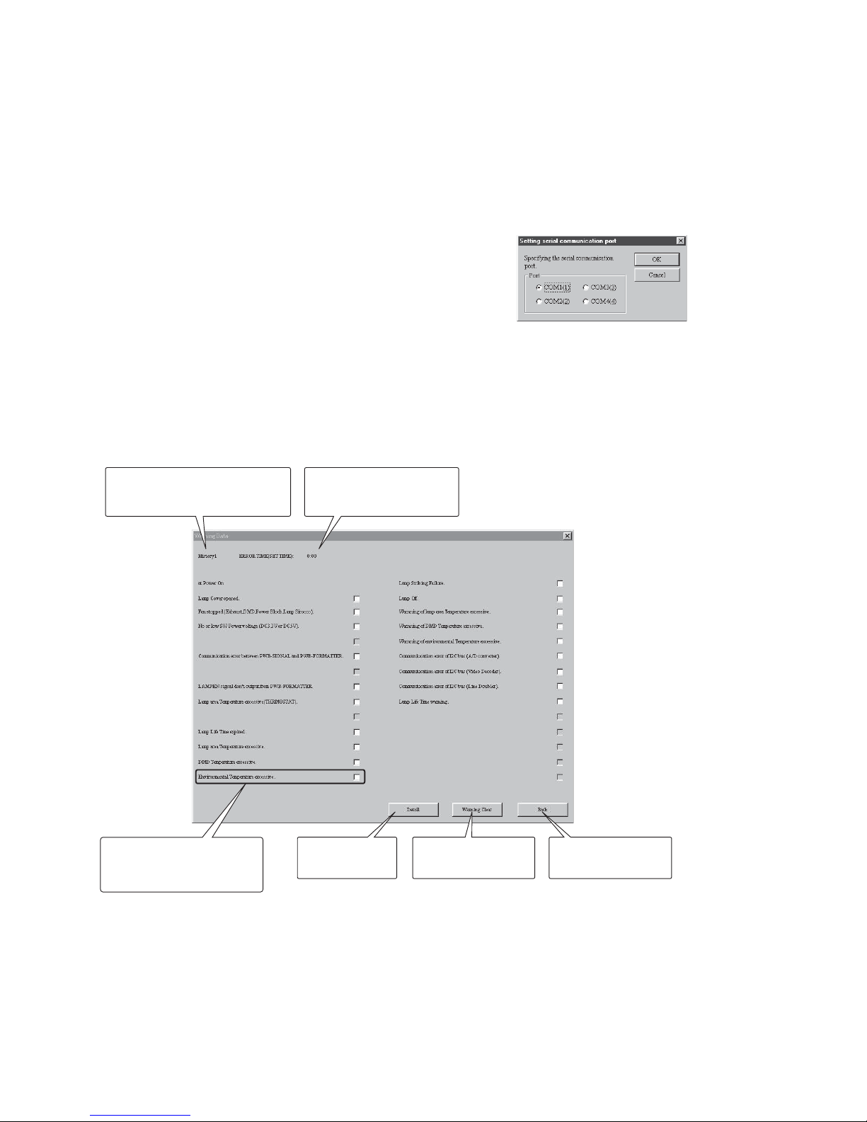
(3) Warning dialog window
1. The warning dialog window displays the error location.
2. “ERROR TIME (SET TIME)” displays the time when the
warning history data were saved (,or the SET TIME in the
service menu). “ERROR TIME” and “SET TIME” shown in
the main dialog window are useful to know when the error
occurred.
3. Pressing the Detail button activates Notepad and opens
the file containing the information about the set and the
warning data. To prevent writing over this file, be sure
to select “Save As” from “File” of the menu in Notepad to
save the file. The name of the file being displayed should
be “DataTemp.txt.”
4. Pressing the [Warning Clear] button displays the confirmation message window, which asks you whether you will
clear the warning history data. Press the [OK] button to
clear the warning history data or the [Cancel] button to
cancel clearing them.
5. Pressing the [Back] button displays the main dialog window again and carries out communication with the projector again to get information from it.
(4) Switching the COM port
1. Select the serial port to which the cable is being connected. When the selected serial port isn’t available or doesn’t
exist, an error message window is displayed.
2. Press the [OK] button to switch the COM port. When the
serial port is switched correctly, communication with the
projector is carried out again to get information from it.
COM port switching dialog window
Goes back to the
main dialog window.
Clears all the
warning history data.
Creates a
detailed report.
All the error items are
displayed in red and their
check boxes are checked.
Indicates which data of the
Warning Status 1, 2, or 3 are
displayed.
Displays the SET TIME
when the warning history
data were saved.
Warning dialog window
The information to
be displayed varies depending on
the model.
Page 14

- 5 -
SPECIFICATION OF RGB SIGNALS IN EACH COMPUTER MODE OF THE PROJECTOR
Specifi cation of RGB signals in each computer mode of the projector
Signal mode Resolution
(H x V)
Horizontal
frequency (kHz)
Vertical frequency
(Hz)
Normal mode
(H x V)
Real mode
(H x V)
TV60, 480i (525i) 720 x 480 15.73 59.94 1024 x 768 640 x 480 *1
TV50, 576i (625i) 720 x 576 15.63 50.00 1024 x 768 768 x 576 *1
1080i60 (1125i60) 1920 x 1080 33.75 60.00 1024 x 576 1024 x 768 *1, *2
1080i50 (1125i50) 1920 x 1080 28.13 50.00 1024 x 576 1024 x 768 *1, *2
480p (525p) 720 x 480 31.47 59.94 1024 x 768 640 x 480 *1, *2
576p (625p) 720 x 576 31.25 50.00 1024 x 768 768 x 576 *1, *2
720p60 (750p60) 1280 x 720 45.00 60.00 1024 x 576 1024 x 720 *2, *3
720p50 (750p50) 1280 x 720 37.50 50.00 1024 x 576 1024 x 720 *2, *3
1080p60 (1125p60) 1920 x 1080 67.50 60.00 1024 x 576 1024 x 768 *2, *3
1080p50 (1125p50) 1920 x 1080 56.25 50.00 1024 x 576 1024 x 768 *2, *3
CGA70 640 x 400 31.47 70.09 1024 x 640 640 x 400
CGA84 640 x 400 37.86 84.13 1024 x 640 640 x 400
CGA85 640 x 400 37.86 85.08 1024 x 640 640 x 400
VGA60 640 x 480 31.47 59.94 1024 x 768 640 x 480 *2
VGA72 640 x 480 37.86 72.81 1024 x 768 640 x 480
VGA75 640 x 480 37.50 75.00 1024 x 768 640 x 480
VGA85 640 x 480 43.27 85.01 1024 x 768 640 x 480
SVGA56 800 x 600 35.16 56.25 1024 x 768 800 x 600
SVGA60 800 x 600 37.88 60.32 1024 x 768 800 x 600 *2
SVGA72 800 x 600 48.08 72.19 1024 x 768 800 x 600
SVGA75 800 x 600 46.88 75.00 1024 x 768 800 x 600
SVGA85 800 x 600 53.67 85.06 1024 x 768 800 x 600
SVGA95 800 x 600 59.97 94.89 1024 x 768 800 x 600
XGA60 1024 x 768 48.36 60.00 1024 x 768 1024 x 768 *2
XGA70 1024 x 768 56.48 70.07 1024 x 768 1024 x 768
XGA75 1024 x 768 60.02 75.03 1024 x 768 1024 x 768
XGA85 1024 x 768 68.68 85.00 1024 x 768 1024 x 768
SXGA70a 1152 x 864 63.85 70.01 1024 x 768 1024 x 768
SXGA75a 1152 x 864 67.50 75.00 1024 x 768 1024 x 768
SXGA85a 1152 x 864 77.49 85.06 1024 x 768 1024 x 768
WXGA60 1280 x 768 47.78 59.87 1024 x 614 1024 x 768 *2
WXGA60a 1280 x 800 49.70 59.81 1024 x 640 1024 x 768 *2
WXGA60b 1360 x 768 47.71 60.02 1024 x 578 1024 x 768
WXGA60c 1366 x 768 47.50 59.75 1024 x 576 1024 x 768
WXGA+60 1440 x 900 55.94 59.89 1024 x 640 1024 x 768
SXGA60b 1280 x 960 60.00 60.00 1024 x 768 1024 x 768
SXGA75b 1280 x 960 75.00 75.00 1024 x 768 1024 x 768
SXGA85b 1280 x 960 85.94 85.00 1024 x 768 1024 x 768
SXGA60 1280 x 1024 63.98 60.02 960 x 768 1024 x 768 *2
SXGA75 1280 x 1024 79.98 75.02 960 x 768 1024 x 768
SXGA85 1280 x 1024 91.15 85.02 960 x 768 1024 x 768
SXGA+60
1400 x 1050 63.98 60.02 1024 x 768 1024 x 768
1400 x 1050 65.32 59.98 1024 x 768 1024 x 768 *2
SXGA+75 1400 x 1050 82.28 74.87 1024 x 768 1024 x 768
WSXGA+60 1680 x 1050 65.29 59.95 1024 x 640 1024 x 768
MAC13 640 x 480 35.00 66.67 1024 x 768 640 x 480
MAC16 832 x 624 49.72 74.55 1024 x 768 832 x 624
MAC19 1024 x 768 60.24 75.02 1024 x 768 1024 x 768
HP75 1024 x 768 62.94 74.92 1024 x 768 1024 x 768
HP72 1280 x 1024 78.13 72.00 960 x 768 1024 x 768
SUN66a 1152 x 900 61.85 66.00 984 x 768 1024 x 768
SUN76a 1152 x 900 71.81 76.64 984 x 768 1024 x 768
SUN66 1280 x 1024 71.68 66.68 960 x 768 1024 x 768
SUN76 1280 x 1024 81.13 76.11 960 x 768 1024 x 768
SGI72 1280 x 1024 76.92 72.30 960 x 768 1024 x 768
SGI76 1280 x 1024 82.01 76.00 960 x 768 1024 x 768
UXGA60 1600 x 1200 75.00 60.00 1024 x 768 1024 x 768 *2
*1: The PinP mode and the MAGNIFY mode don’t function with this signal.
*2: Available with the signal for the DVI-D terminal.
*3: You can select from two adjustment modes by pressing the AUTO POSITION button. (For details, see page 16.) When the
VIDEO SIGNAL mode is selected, the PinP mode and the MAGNIFY mode don’t function.
Page 15

- 1 -
Program ROM : LC6 Ver. 2.1
Program
No.
Pattern
15
Every other horizontal line (Red)
16
Every other horizontal line (Green)
17
Every other horizontal line (Blue)
29 White / black signal
30 SMPTE (White) *
* Though the signal generator supplies this signal
as a green signal, the projector receives it as
Y/CB/CR signal. Therefore, this signal is projected as a full white SMPTE signal.
Timing of XGA signal (Vertical frequency 60 Hz)
DOT-CLOCK [MHz] 65.0 VP [H] 806
HP [DOT] 1344 VDISP [H] 768
HDISP [DOT] 1024 VDW [H] 6
HDW [DOT] 136 VBP [H] 29
HBP [DOT] 160 Interlace ---
Signal polarity HD :-, VD : -
Timing of NTSC (480i) signal (Vertical frequency 59.94 Hz)
DOT-CLOCK [MHz] 13.5 VP [H] 525
HP [DOT] 858 VDISP [H] 480
HDISP [DOT] 720 VDW [H] 3
HDW [DOT] 64 VBP [H] 14
HBP [DOT] 58 Interlace Interlace
Signal polarity
HD :nothing
VD : nothing
Sync on green : -
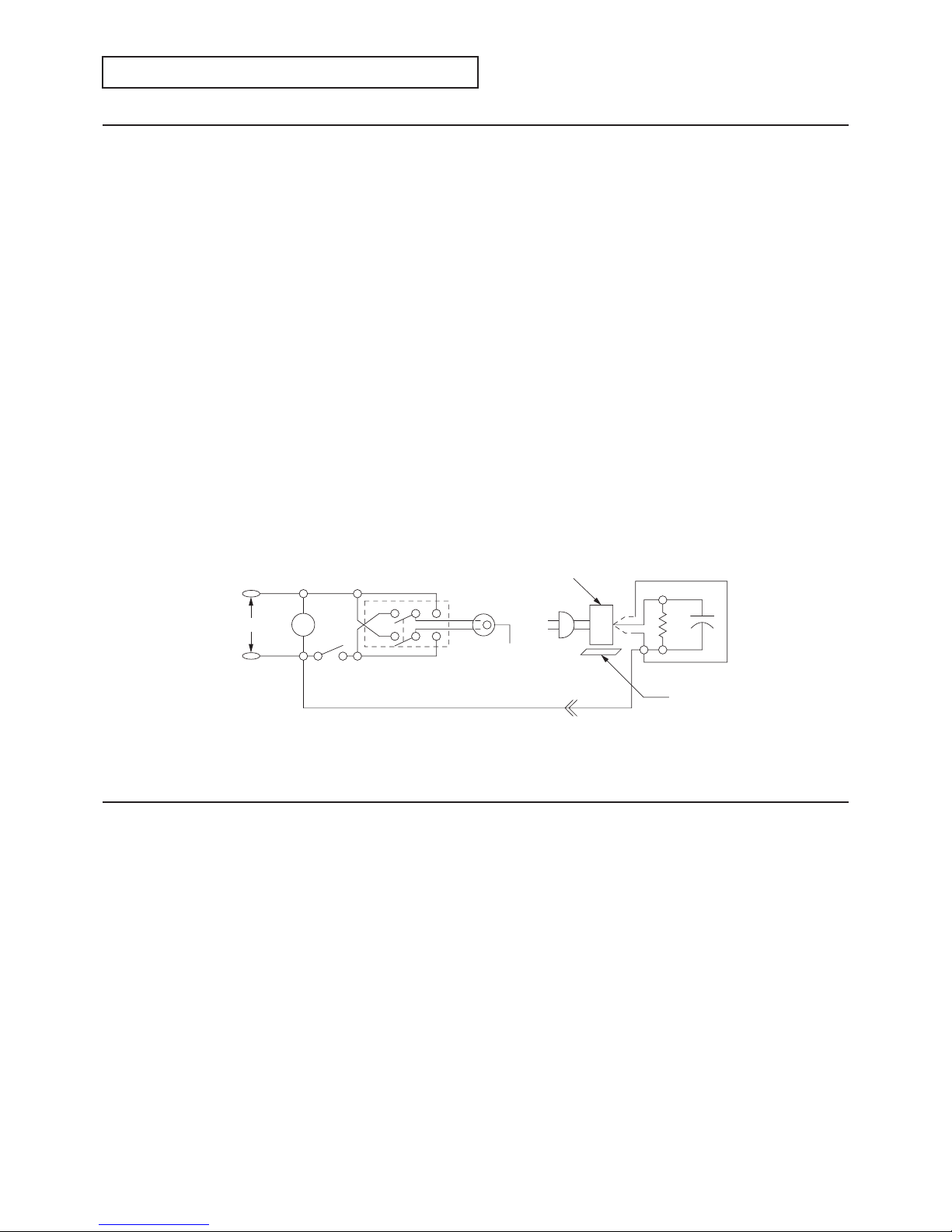
ELECTRICAL ADJUSTMENTS
All the electrical adjustments for this projector require the communication program [Hyper Terminal] of Microsoft® Windows®
95/98/Me/XP operating system.
Necessary Equipment and Connecting
Connect the following equipment as shown in the right fi gure.
• This projector
• Personal computer (running Microsoft
®
Windows® 95/98/
Me/XP operating system)
• RS-232C cable
• Signal generator (equivalent to VG-812)
• PC monitor
Test Signal
• XGA signal (vertical frequency:60Hz) / NTSC signal (vertical frequency:59.94Hz)
The timing and patterns for the adjustment are as follows :
HDISP
HP
HBP
HDW
VDISP
VP
VBP
VDW
HD signal
H Timing V Timing
VD signal
Personal
computer
PC
monitor
COMPUTER IN
terminal
Projector
Signal
generator
RS-232C cable
RS-232C input
terminal
Page 16

- 2 -
Adjustment with Microsoft® Windows® 95/98/Me/XP Operating System
1. Starting
1. Start Windows® 95/98/Me/XP.
2. Select [Start] - [Programs] - [Accessories] - [Communications] - [Hyper Terminal] in order.
The [Connection Description] window will open.
Note:
You can select [Start] - [Programs] - [Accessories] - [Hyper Terminal] in order and double-click [hypertrm.exe] in Windows®95.
2. Hyper Terminal Setting
1. Make settings on the [Connection Description] window referring to the table on the
right.
Item Setting
Connection Port (COM1-COM4)
Port settings : Bits per second
: Data bits
: Parity
: Stop bits
: Flow
9600
8
None
1
control
Settings : Emulation VT100
ASCII setup : ASCII Sending
: ASCII Receiving
Send line ends with line feeds
Echo typed characters locally
Line delay :
1000 milliseconds
Character delay : 10 milliseconds
Append line feeds to incoming line ends
3. Adjustment
Type the adjustment command and the adjustment value on the Hyper Terminal window in capital alphanumeric letters, and
press the [ENTER] key.
4. Writing Adjustment Value
Type the adjustment command and the adjustment value on the Hyper Terminal window in capital alphanumeric letters, and
press the [ENTER] key.
Note: This step is not necessary for “ADC offset/gain adjustment,” which is carried out automatically.
5. Closing
Click on the Close button in the upper-right corner of the window to exit the Hyper Terminal.
Close all the opening windows before exiting Windows
®
95/98/Me/XP.
Page 17
- 3 -
[A/D Pre-Amplifi cation Circuit]
1. ADC offset/gain adjustment
To adjust the DC level and amplitude of the video signal at the time of ADC input.
Solid black, solid white, or incorrect color phase appear in the projected im-
age.
Measuring
instrument
-----
Test point -----
EXT trigger
-----
Measurement
range
-----
Input signal
Shown in the table
below
Input terminal
COMPUTER 2
IN terminal
Adjustment purpose
Symptom when
incorrectly adjusted
* Enter the adjustment commands in capital alphanumeric letters.
1. Connect the projector with a PC running Microsoft
®
Windows®95/98/Me/XP operat-
ing system. (Refer to the fi gure on page 1.)
2. Start Microsoft
®
Windows® 95/98/Me/XP.
3. Start the communication program [Hyper Terminal] on Microsoft
®
Windows®95/98/
Me/XP to open the Hyper Terminal window. (Refer to Hyper Terminal Setting on
page 2 for the settings.)
Offset/gain adjustment with the RGB signal supplied
4. Supply an XGA signal (White/black raster No. 29).
5. Enter [00~5] (the command for RGB input offset/gain adjustment) on the Hyper Terminal window, and the adjustment proceeds automatically.
6. When the adjustment fi nishes, the return command [00~5111] is displayed on the
Hyper Terminal window. The last three digits of the return command indicate the
adjustment results of R, G, and B respectively from the left by 1 or 0. When the
adjustment has succeeded, 1 is displayed. When it has failed, 0 is displayed. Possible causes of failures in the adjustment are errors on the PCBs, wrong signals,
and wrong input selection.
Offset adjustment with the component video signal supplied
7. Supply an NTSC signal (SMPTE (White), No. 30).
8. Enter [00~AC1] (the command for video input clamp adjustment) on the Hyper Terminal window, and the adjustment proceeds automatically.
9. When the adjustment finishes, the return command [00~AC111] is displayed on
the Hyper Terminal window. The last two digits of the return command indicate the
adjustment results of CR and CB respectively from the left by 1 or 0. When the
adjustment has succeeded, 1 is displayed. When it has failed, 0 is displayed. Possible causes of failures in the adjustment are errors on the PCBs, wrong signals,
and wrong input selection.
Adjustment Procedures
No. Pattern
29 White/black raster
30 SMPTE (White)*
* Though the signal generator supplies this signal as a green signal,
the projector receives it as Y/CB/CR
signal. Therefore, this signal is projected as a full white SMPTE signal.
Page 18
- 4 -
[Liquid Crystal Panel Driving
Adjustment Circuit]
2. Flicker
To remove fl ickers form the screen.
Flickers appear.
Measuring
instrument
-----
Test point -----
EXT trigger
-----
Measurement
range
-----
Input signal
Shown in the table
below
Input terminal
COMPUTER 2
IN terminal
Adjustment purpose
Symptom when
incorrectly adjusted
* Make this adjustment only when fl ickers remarkably appear on the screen.
* Enter the adjustment commands and adjustment values of the hexadecimal number
in capital alphanumeric letters.
* Carry out this adjustment after running the projector for 2 minutes or more supply-
ing the specifi ed test signal to it.
1. Connect the projector with a PC running Microsoft
®
Windows®95/98/Me/XP operat-
ing system. (Refer to the fi gure on page 1.)
2. Start Microsoft
®
Windows®95/98/Me/XP.
3. Start the communication program [Hyper Terminal] on Microsoft
®
Windows®95/98/
Me/XP to open the Hyper Terminal window. (Refer to Hyper Terminal Setting on
page 2 for the settings.)
4. Set the following items in the IMAGE menu.
CONTRAST 0
BRIGHTNESS 0
COLOR TEMP STANDARD
5. Project an image onto the screen.
6. Enter the fl icker adjustment mode command [00~3100008AFC] on the Hyper Termi-
nal window to make the fl ickers easy to view.
Red
7. Supply an XGA signal (Every other horizontal line (Red), No. 15).
8. Enter the adjustment command [00~217
] on the Hyper Terminal window to mini-
mize the red fl ickers. For
,select a value that reduces the fl ickers most*. (Enter a
value from [56] to [72] (HEX).)
9. Enter the writing command [00~1044
] on the Hyper Terminal window to write the
new value into the E
2
PROM.
Enter the value that was entered in step 8 in .
Green
10. Supply an XGA signal (Every other horizontal line (Green), No. 16).
11. Enter the adjustment command [00~237
] on the Hyper Terminal window to mini-
mize the green fl ickers. For
,select a value that reduces the fl ickers most*. (Enter
a value from [56] to [72] (HEX).)
12. Enter the writing command [00~1045
] on the Hyper Terminal window to write the
new value into the E
2
PROM.
Enter the value that was entered in step 11 in *.
Blue
13. Supply an XGA signal (Every other horizontal line (Blue), No. 17).
14. Enter the adjustment command [00~257
] on the Hyper Terminal window to mini-
mize the green fl ickers. For
, select a value that reduces the fl ickers most*. (Enter
a value from [56] to [72] (HEX).)
15. Enter the writing command [00~1046
] on the Hyper Terminal window to write the
new value into the E
2
PROM.
Enter the value that was entered in step 14 in *.
16. Enter the fl icker adjustment mode cancel command [00~310000AAFC] on the Hy-
per Terminal window to go back to the regular screen.
* When the command is sent successfully, such command is returned as it is after
sending. You can check the current value by sending the command without entering
any value in .
No. Pattern
15
XGA Every other horizontal line (Red)
16
XGA Every other horizontal line (Green)
17
XGA Every other horizontal line (Blue)
Every other horizontal line pattern
Page 19

- 1 -
Microsoft Windows 95/98/Me/XP are either registered trademarks or trademarks of Microsoft Corporation in the United States
and/or other countries.
Other brand or product names are trademarks or registered trademarks of their respective holders.
TRADEMARK, REGISTERED TRADEMARK
Many electrical and mechanical parts in the projector have special safety related characteristics. These characteristics are often
not evident from visual inspection nor can the protection afforded by them necessarily be obtained by using replacement components rated for higher voltage, etc. Replacement parts which have these special safety characteristics are identifi ed in this ser-
vice manual. Electrical components having such features are identifi ed by shading on the schematic diagram and the parts list
of this service manual and by the supplementary sheet for this chassis to be issued subsequently.
PRODUCT SAFETY NOTICE
Page 20
- 2 -
Europe, other than USA
NOTICE: Observe all cautions and safety related notes located inside the cabinet and on the chassis.
Warning
1. An isolation transformer should be used between the projector and the AC supply point before any test/service is performed
on a LIVE chassis projector.
2. Operation of this projector outside the cabinet or with the cover removed, involves a shock hazard from the projector power
supplies. Work on the projector should not be attempted by anyone who is not thoroughly familiar with precautions necessary when working on high voltage equipment.
3. When service is required, observe the original lead dressing. Extra precaution should be given to assure correct lead dressing in the high voltage area. Where a short-circuit has occurred, replace those components that indicate evidence of overheating.
Leakage current cold check
Before returning the projector to the customer, it is recommended that leakage current be measured according to the following
methods.
With the AC plug removed from the AC source, place a jumper across the two AC plug prongs. Turn the projector AC switch on.
Using an 500 V D.C. Insulation Tester, connect one lead to the jumpered AC plug and touch the other lead to each exposed metal part (screwheads, etc.), particularly any exposed metal part having a return path to the chassis. Exposed metal parts having a
return path to the chassis should have a minimum resistance reading of 4 megohm. Any resistance below this value indicates an
abnormality which requires corrective action.
V
S1
S2
GH
(grounding)
open
Grounding supply conductor
B
Insulating table
Projector
A
AC milliammeter
Figure
A
C 100 to 240 V
North america
NOTICE: Observe all cautions and safety related notes located inside the cabinet and on the chassis.
Warning
1. Operation of this projector outside the cabinet or with the cover removed presents a shock hazard from the projector power
supplies.
2. When a short-circuit has occurred, replace those components that indicate evidence of overheating.
3. Grounding circuit continuity is vital for safe operation of equipment. Do not remove ground connection while the power cord
is still connected to the supply. Disconnect supply before servicing.
Leakage current check
Before returning the projector to the customer, it is recommended that leakage current be measured according to the following methods.
1. Cold check
With the AC plug removed from the AC 100 to 240 V, place a jumper across the two AC plug prongs. Turn the projector AC
switch on. Using an ohm-meter, connect one lead to the AC plug and touch the other lead to each exposed metal part (metal
cabinet, screwheads, metal overlays, etc.), particularly any exposed metal part having a return path to the chassis. Exposed
metal parts having a return path to the chassis should have a minimum resistance reading of 1 megohm. Any resistance below this value indicates an abnormality which requires corrective action. Exposed metal parts not having a return path to the
chassis will indicate an open circuit.
2. Hot check
Use the circuit in fi gure to perform this test.
(1) With switch S1 open, connect the projector to the measuring circuit. Immediately after connection, measure the leakage
current using both positions of switch S2, and with the switching devices in the projector in all of their operating positions.
(2) Switch S1 is then closed, energizing the projector. Immediately after closing the switch, measure the leakage current us-
ing both positions of switch S2, and with the switching devices in the projector in all of their operating positions. Current
measurements of items (1) and (2) are to be repeated after the projector has reached thermal stabilization. The leakage
current must not be more than 0.5 milliampere.
SAFETY PRECAUTIONS
Page 21
- 3 -
Lead-free solder is handled in a different way from eutectic solder. See below for details.
How to distinguish circuit boards using lead-free solder from those using
eutectic solder
Circuit boards using lead-free solder
A mark of Solder, Joints, PCA or LFS (for limited marking space) is printed near the board assembly number on
the component side.
Circuit boards using eutectic solder
Circuit boards using eutectic solder are divided into two groups.
- Boards having no mark of
Solder, Joints, PCA or LFS (for limited marking space) near the board assembly
number.
- Boards having a mark of
Solder, Joints, PCA or LFS (for limited marking space) that is painted out by a felt-
pen near the board assembly number.
* Only when there is a limited marking space on the board,
Solder may be indicated as S, Joints as J, and
PCA as P.
* Circuit boards using lead-free solder and those using eutectic solder may be used together in the same product.
Instructions for resoldering
- For circuit boards using lead-free solder, use lead-free solder.
- For circuit boards using eutectic solder, use eutectic solder.
- Separate the soldering iron for lead-free solder from that for eutectic solder completely for use.
(It is prohibited to use a same soldering iron for lead-free solder and eutectic solder.)
- For lead-free solder, it is advisable to use a soldering iron of at least 40 W because lead-free solder has a melting point approx. 35°C higher than that of eutectic solder as conventionally used. For wire solder, use M705ESC made by Senju Metal
Industry Co., Ltd.
- To remove solder, you can use desoldering wires for eutectic solder as conventionally used.
PRECAUTIONS FOR RESOLDERING
Page 22
- 4 -
PCB LOCATION
Fig.1
1
2
3
4
5
6
7
8
9
10
11
12
13
14
Page 23

- 5 -
Parts list : See page 2 of PARTS LIST
Item No. Part name
1 IRF PCB ASSY
2 FILTER PCB ASSY
3 POWER PCB ASSY
4 MAIN PCB ASSY
5 DRIVE PCB ASSY
6 IRR PCB ASSY
7 KEY PCB ASSY
8 TERMINAL PCB ASSY
9 BOO PCB ASSY
10 BOO SUB PCB ASSY
11 Lamp power unit
12 INLET PCB ASSY
13 POWER SUB PCB ASSY
14 MOTOR PCB ASSY
Table 1
Page 24
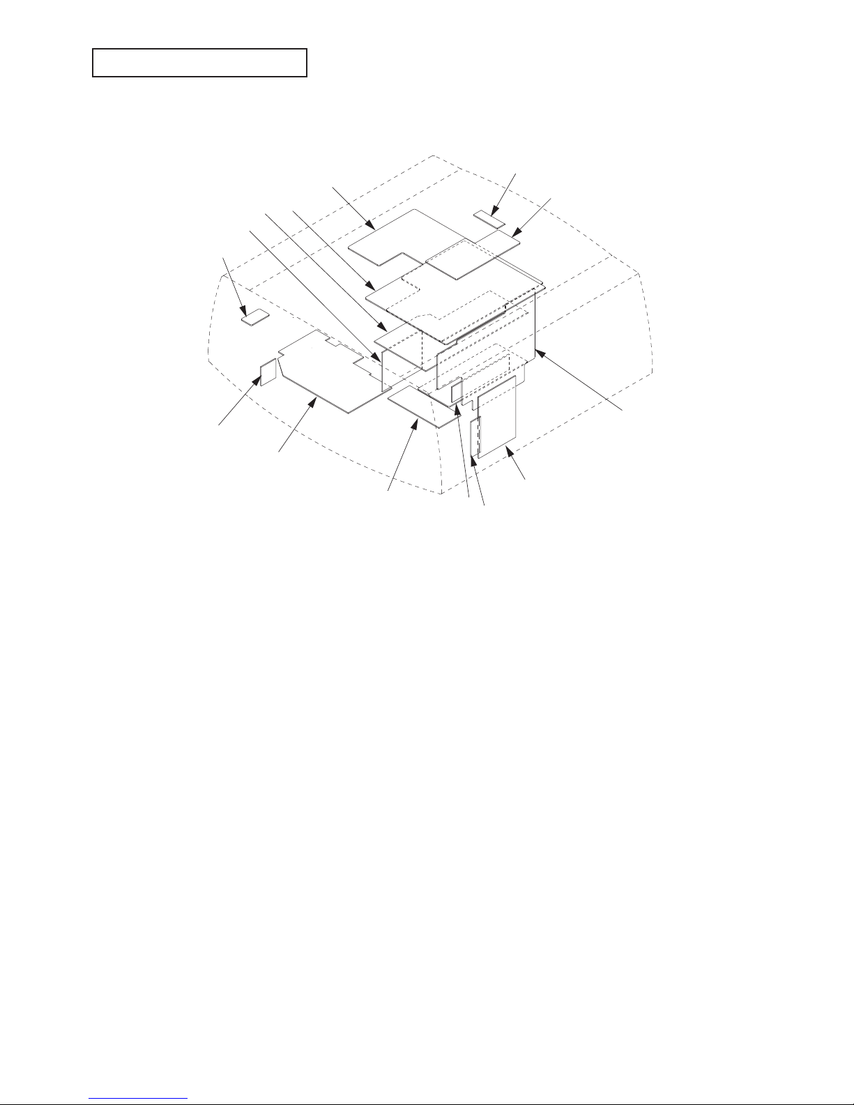
- 6 -
EXPOSED VIEW
Fig.2-1
1
2
A
x6
3
Bx3
4
5
6
7
8
9
Cx4
Dx2
Ex2
Fx1
Gx2
Hx3
10
11
14
Jx3
Kx3
Lx4
Mx2
12
13
L VP ASSY
Page 25

- 7 -
Part name Number of screw
1.Front case ASSY None
2.Lens cap None
3.Front case unit Ax6
4.Terminal cover unit Bx3
5.Alarm unit ASSY Cx4
6.Alarm cover U Dx2
7.BOO PCB ASSY Ex2
8.BOO SUB PCB ASSY Fx1
9.Alarm cover L None
10.Sensor Gx2
11.Top case ASSY None
12.Top cover unit Hx3
13.Top case unit Jx3,Kx3,Lx4
14.KEY PCB ASSY Mx2
Table 2-1
Parts list : See page 3 of PARTS LIST
Page 26
- 8 -
Chassis 1 ASSY
Fig.2-2
1
Ax1
Bx2
2
Cx5
3
4
Dx3
Ex3
Fx3
5
6
Gx1
Hx2
7
8
Jx8
Kx2
Lx4
9
10
11
12
13
14
Mx2
Nx3
Px3
Qx1
15
Rx1
16
17
18
19
20
21
Sx1
22
Tx2
Ux5
Vx1
23
Page 27

- 9 -
Part name Number of screw
1.Terminal board unit Ax1,Bx2
2.Main barrier Cx5
3.Spacer cushion None
4.T erminal ASSY Dx3,Ex3,Fx3
5.Gum spacer None
6.Main radiator Gx1
7.Main PCB holder Hx2
8.DRIVE PCB ASSY Jx8
9.Drive PCB holder Kx2,Lx4
10.Drive fan ASSY None
11.Fan holder L Mx2
12.Drive fan Nx3
13.Fan PCB duct Px3
14.Shield holder Qx1
15.IRR PCB ASSY Rx1
16.Speaker ASSY None
17.Speaker None
18.Bush SP None
19.Holder SP Sx1
20.Lead clamper None
21.Thermo barrier None
22.Lamp power lead Tx2
23.Optical unit Ux5,Vx1
Table 2-2
Parts list : See page 4 of PARTS LIST
Page 28
- 10 -
1
2
Ax1
3
4
5
6
7
8
9
Bx2
Cx1
Dx1
Ex2
Fx4
10
Gx5
Hx1
11
Jx2
Kx2
12
13
14
15
16
17
18
19
20
Lx1
Mx1
Nx1
Qx3
21
Px1
Chassis 2 ASSY
Fig.2-3
Page 29

- 11 -
Part name Number of screw
1.Bottom case ASSY None
2.IRF PCB ASSY Ax1
3.Front holder L Bx2
4.Motor PCB holder Cx1
5.MOTOR PCB ASSY Dx1
6.Power fan ASSY None
7.Fan holder F Ex2
8.Power fan Fx4
9.Fan guard None
10.POWER SUB PCB ASSY Gx5,Hx1
11.Power shield L Jx2,Kx2
12.SW shield None
13.Power box T unit None
14.POWER PCB ASSY Lx1
15.Power fi n None
16.Lamp power unit None
17.FILTER PCB ASSY Mx1
18.Seesaw switch None
19.INLET PCB ASSY Nx1,Px1
20.Power box B unit Qx3
21.Bottom case unit None
Table 2-3
Parts list : See page 5 of PARTS LIST
Page 30
- 12 -
Bottom case unit
Fig.2-4
Part name Number of screw
1.Filter unit None
2.Fan fi lter None
3.Lamp cover unit Ax1
4.Fan cushion None
5.SW holder Bx2
6.Micro SW None
7.Micro SW None
8.Adjustment foot ASSY Cx3
9.Adjustment foot ASSY Dx3
10.Adiuster unit None
11.Adiuster unit None
Parts list : See page 6 of PARTS LIST
Table 2-4
1
2
3
4
5
6
7
8
9
10
11
Ax1
Bx2
Cx3
Dx3
Page 31

- 13 -
1
2
3
4
5
Ax2
Bx4
Cx1
Dx8
Ex4
Fx1
Gx1
Hx1
Jx2
Part name Number of screw
1.MAIN PCB ASSY Ax2,Bx4,Cx1
2.Terminal holder Dx8,Ex4,Fx1,Gx1,Hx1
3.Pin jack shield None
4.TERMINAL PCB ASSY Jx2
5.PCB holder None
Parts list : See page 6 of PARTS LIST
Table 2-5
T erminal ASSY
Fig.2-5
Page 32

- 14 -
1
2
3
4
5
6
7
8
9
10
11
12
13
14
15
16
17
18
19
20
21
22
Ax1
Bx1
Cx2 Dx2
Ex2
Fx2
Gx2
Hx4
Jx2
Kx3
Lx6
Mx2
Nx4
Px3
Qx3
Rx2
Sx1
Tx4
Ux2
Vx2
Wx2
Yx1
Zx1
Optical unit 1
Fig.2-6
Page 33

- 15 -
Part name Number of screw
1.Lamp duct Ax1,Bx1
2.Lamp cover T duct Cx2
3.Thermistor Dx1
4.Thermostat Dx2
5.PBS fan Ex2
6.Lamp fan Fx2
7.PBS duct Gx2
8.Grille Hx4
9.Exhaust duct Jx2
10.Exhaust fan None
11.Lamp cover T Kx3
12.Sub frame cover Lx6,Mx2
13.Sub frame Nx4
14.LCD fan Px3
15.LCD block Qx3
16.Lamp case ASSY Rx2
17.Lamp Sx1
18.Lens unit Tx4
19.Zoom focus motor Ux2
20.Lens shift motor Vx2,Wx2
21.LCD duct Yx1,Zx1
22.Main F shift base None
Table 2-6
Parts list : See page 7 of PARTS LIST
Page 34

- 16 -
Optical unit 2
Fig.2-7
1
2
3
4
5
6
7
8
9
10
11
12
Ax2
Bx
1
Cx1
Dx1
Ex1
Fx1
Gx1
Hx1
Jx1
Kx1
123 7,8,9 10,11,12
4,5,6
4,7,10 :
5,8,11 :
6,9,12 :
Light source side(Lamp side)
Dlrections which the setting parts face in
Projection side(Lamp side)
In possible
directions
Flat surface Flat surface
Flat surface Flat surface
Flat surface
Marking Color marking
Color marking Color marking
Color marking
Convex
Uneven surface
Surface to stick
the polarizer on
Surface to stick
the polarizer on
Surface to stick
the polarizer on
Shaved edge
Blue
Green
Red
Page 35

- 17 -
Part name Number of screw
1.PBS ASSY None
2.Multi lens B None
3.Multi lens A Ax2
4.Polarizer (B) IN Bx1
5.Polarizer (G) IN Cx1
6.Polarizer (R) IN Dx1
7.Polarizer (B) OUT Ex1
8.Polarizer (G) OUT Fx1
9.Polarizer (R) OUT Gx1
10.Polarizer (B) PURI Hx1
11.Polarizer (G) PURI Jx1
12.Polarizer (R) PURI Kx1
Parts list : See page 8 of PARTS LIST
Table 2-7
POSITION ADJUSTMENT OF MULTI LENS A
ax2
b
c
d
x2
Multi lens
A
Follow the steps below for the adjustment after replacing the
multi lens A.
Number of jig screw : 859C746O10
1. Fasten two screws (a) to secure the Multi lens A
temporarily.
2. Project a full white raster on the screen.
3. Adjust the position of the multi lens A to correct color
unevenness near the screen edges.
To adjust the vertical position, turn the screw (b).
To adjust the horizontal position, use the jig screw (c).
4. Fasten two screws (a) and two screws (d) tightly to
secure the Multi Lens A fi rmly.
Page 36

- 18 -
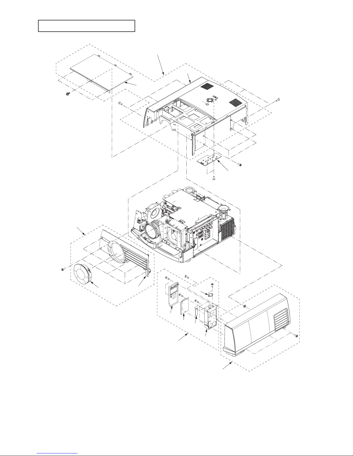
DISASSEMBLY
ax3
A
B
Terminal cover ASSY
1. Removal of the terminal cover
ASSY
1. Loosen the three screws (a) as shown in Fig. 3-1.
2. Open the bottom of the terminal cover ASSY outward
(as shown by the arrow (A)) as shown in Fig. 3-1.
3. Slide the top of the terminal cover ASSY to the front
for removal (as shown by the arrow (B)) as shown in
Fig. 3-1.
Fig. 3-1
ax4
bx2
cx2
dx1
Alarm unit ASSY
Alarm cover U
BOO PCB ASSY
BOO SUB PCB ASSY
Fig. 3-2
2. Removal of the BOO PCB ASSY
and BOO SUB PCB ASSY
1. Remove the terminal cover ASSY according to “1.
Remove of the terminal cover ASSY”.
2. Remove the four screws (a) as shown in Fig. 3-2.
3. Remove the alarm unit ASSY as shown in Fig. 3-2.
4. Remove the two screws (b) as shown in Fig. 3-2.
5. Remove the alarm cover U as shown in Fig. 3-2.
6. Remove the two screws (c) as shown in Fig. 3-2.
7. Remove the BOO PCB ASSY as shown in Fig. 3-2.
8. Remove the screw (d) as shown in Fig. 3-2.
9. Remove the BOO SUB PCB ASSY as shown in Fig.
3-2.
Page 37

- 19 -
ax6
bx3
cx4
dx2
A B
C
D
E
MA
Top cover unit
Lens unit
Zoom focus motor
Front case unit
3. Removal of the lens unit and
zoom focus motor
1. Remove the six screws (a) as shown in Fig. 3-3.
2. Pull the top and left side of the front case unit (as
shown by the arrow (A)) as shown in Fig. 3-3.
3. Raise the left side of the front case unit (as shown by
the arrow (B)) as shown in Fig. 3-3.
4. Pull the left side of the front case unit to front for re-
moval (as shown by the arrow (c)) as shown in Fig.
3-3.
5. Remove the three screws (b) as shown in Fig. 3-3.
6. Slide the top cover unit to the front (as shown by ar-
row (D)) as shown in Fig. 3-3.
7. Remove the top cover unit to upward (as shown by
the arrow (E)) as shown Fig. 3-3.
8. Disconnect the connector (MA) as shown in Fig. 3-3.
9. Loosen the four screws (c) as shown in Fig. 3-3.
10. Remove the lens unit as shown Fig. 3-3.
11. Remove the two screws (d) as shown in Fig. 3-3.
12. Remove the zoom focus motor as shown in Fig. 3-3.
Fig. 3-3
Page 38

- 20 -
ax3
bx3
cx4
dx2
ST
Top case unit
KEY PCB ASSY
4. Removal of the top case unit and
KEY PCB ASSY
1. Remove the terminal cover ASSY according to “1.
Removal of the terminal cover ASSY”.
2. Remove the front case unit and top cover unit ac-
cording to “3. Removal of the lens unit and zoom focus motor”.
3. Remove the three screws (a), three screws (b) and
four screws (c) as shown in Fig. 3-4.
4. Disconnect the connector (ST) as shown in Fig. 3-4.
5. Remove the top case unit as shown in Fig. 3-4.
6. Remove the two screws (d) as shown in Fig. 3-4.
7. Remove the KEY PCB ASSY as shown in Fig. 3-4.
Fig. 3-4
Page 39

- 21 -
ax1
cx1
bx1
dx1
MA
MV
AL
AM
IRR PCB ASSY
IRF PCB ASSY
MOTOR PCB ASSY
Motor PCB holder
5. Removal of the IRF PCB ASSY
1. Remove the terminal cover ASSY according to “1.
Removal of the terminal cover ASSY”.
2. Remove the front case unit and top cover unit ac-
cording to “3. Removal of the lens unit and zoom focus motor”.
3. Remove the top case unit according to “4. Removal
of the top case unit and KEY PCB ASSY”.
4. Remove the screw (a) as shown in Fig. 3-5
5. Disconnect the connector (AM) as shown in Fig. 3-5
6. Remove the IRF PCB ASSY as shown in Fig. 3-5.
6. Removal of the MOTOR PCB
ASSY
1. Remove the terminal cover ASSY according to “1.
Removal of the terminal cover ASSY”.
2. Remove the front case unit and top cover unit ac-
cording to “3. Removal of the lens unit and zoom focus motor”.
3. Remove the top case unit according to “4. Removal
of the top case unit and KEY PCB ASSY”.
4. Remove the screw (b) as shown in Fig. 3-5.
5. Remove the motor PCB holder as shown in Fig. 3-5.
6. Remove the screw (c) as shown in Fig. 3-5.
7. Disconnect the two connectors (MA and MV) as
shown in Fig. 3-5.
8. Remove the MOTOR PCB ASSY as shown in Fig.
3-5.
7. Removal of the IRR PCB ASSY
1. Remove the terminal cover ASSY according to “1.
Removal of the terminal cover ASSY”.
2. Remove the front case unit and top cover unit ac-
cording to “3. Removal of the lens unit and zoom focus motor”.
3. Remove the top case unit according to “4. Removal
of the top case unit and KEY PCB ASSY”.
4. Removal the screw (d) as shown in Fig. 3-5.
5. Disconnect the connector (AL) as shown in Fig. 3-5.
6. Remove the IRR PCB ASSY as shown in Fig. 3-5.
Fig. 3-5
Page 40

- 22 -
ax2
bx1
TL
Speaker
Bush SP
Terminal board unit
8. Removal of the speaker
1. Remove the terminal cover ASSY according to “1.
Removal of the terminal cover ASSY”.
2. Remove the front case unit and top cover unit ac-
cording to “3. Removal of the lens unit and zoom focus motor”.
3. Remove the top case unit according to “4. Removal
of the top case unit and KEY PCB ASSY”.
4. Remove the two screws (a) and screw (b) as shown
in Fig. 3-6.
5. Remove the terminal board unit as shown in Fig. 3-6.
6. Disconnect the connector (TL) as shown in Fig. 3-6.
7. Remove the bush SP as shown in Fig. 3-6.
8. Remove the speaker as shown in Fig. 3-6.
Fig. 3-6
ax5
bx2
cx4
Main barrier
Fan guard
Power fan
Fan holder F
9. Removal of the power fan
1. Remove the terminal cover ASSY according to “1.
Removal of the terminal cover ASSY”.
2. Remove the front case unit and top cover unit ac-
cording to “3. Removal of the lens unit and zoom focus motor”.
3. Remove the top case unit according to “4. Removal
of the top case unit and KEY PCB ASSY”.
4. Remove the fi ve screws (a) as shown in Fig. 3-7.
5. Remove the main barrier as shown in Fig. 3-7
6. Remove the two screws (b) as shown in Fig. 3.-7.
7. Remove the fan holder F as shown in Fig. 3-7.
8. Remove the four screws (c) as shown in Fig. 3-7.
9. Remove the fan guard and power fan as shown in
Fig. 3-7.
Fig. 3-7
Page 41

- 23 -
ax3
bx2
cx4
dx1
ex3
fx3
gx8
hx4
jx1
kx1
mx1
nx2
TL
TK
TW
SX
SZ
SL
SD
SQ
SF
SC
SE
SA
DWDV
SV SW
SK
MAIN PCB ASSY
TERMINAL
PCB ASSY
Terminal holder
PCB holder
T erminal ASSY
10. Removal of the MAIN PCB ASSY
1. Remove the terminal cover ASSY according to “1.
Removal of the terminal cover ASSY”.
2. Remove the front case unit and top cover unit ac-
cording to “3. Removal of the lens unit and zoom focus motor”.
3. Remove the top case unit according to “4. Removal
of the top case unit and KEY PCB ASSY”.
4. Remove the terminal board unit according to “8. Re-
moval of the speaker”.
5. Remove the main barrier according to “9. Removal of
the power fan”.
6. Remove the three screws (a), two screws (b), four
screws (c) and screw (d) as shown in Fig. 3-8.
7. Disconnect the connectors (SA, SC,SD, SE, SF, SL,
SQ, SX and SZ) as shown in Fig. 3-8.
8. Remove the MAIN PCB ASSY as shown in Fig. 3-8.
Note: The DV-SV connector, DW-SW connector and SK-TK
connector are connected directly each other.
Disconnect these connectors before removing the
MAIN PCB ASSY.
11. Removal of the TERMINAL PCB
ASSY
1. Remove the terminal cover ASSY according to “1.
Removal of the terminal cover ASSY”.
2. Remove the front case unit and top cover unit ac-
cording to “3. Removal of the lens unit and zoom focus motor”.
3. Remove the top case unit according to “4. Removal
of the top case unit and KEY PCB ASSY”.
4. Remove the terminal board unit according to “8. Re-
moval of the speaker”.
5. Remove the main barrier according to “9. Removal of
the power fan”.
6. Remove the three screws (a), three screws (e) and
three screws (f) as shown in Fig.3-8.
7. Disconnect the connectors (SA, SC, SD, SE,SF, SL,
SQ, SX, SZ, TL and TW) as shown in Fig. 3-8.
8. Remove the terminal ASSY as shown in Fig. 3-8.
Note: The DV-SV connector and DW-SW connector are
connected directly each other.
Disconnect these connectors before removing the
terminal ASSY .
9. Remove the two screws (b), four screws (c), screw (d),
eight screws (g), four screws (h), screw (j), screw (k)
and screw (m) as shown in Fig. 3-8.
10. Remove the MAIN PCB ASSY and terminal holder as
shown in Fig. 3-8.
Note: The SK-TK connector are connected directly each
other.
Disconnect these connectors before removing the
MAIN PCB ASSY.
11. Remove the two screws (n) as shown Fig. 3-8.
12. Remove the TERMINAL PCB ASSY as shown Fig.
3-8.
Fig. 3-8
Page 42

- 24 -
ax1
bx2
cx8
dx3
DG
DR
DB
DP
Main radiator
Main PCB holder
LCD block
DRIVE PCB ASS
Y
12. Removal of the DRIVE PCB
ASSY and LCD block
1. Remove the terminal cover ASSY according to “1.
Removal of the terminal cover ASSY”.
2. Remove the front case unit and top cover unit ac-
cording to “3. Removal of the lens unit and zoom focus motor”.
3. Remove the top case unit according to “4. Removal
of the top case unit and KEY PCB ASSY”.
4. Remove the terminal board unit according to “8. Re-
moval of the speaker”.
5. Remove the main barrier according to “9. Removal of
the power fan”.
6. Remove the terminal ASSY according to “11. Remov-
al of the TERMINAL PCB ASSY”.
7. Remove the screw (a) as shown in Fig. 3-9.
8. Remove the main radiator as shown in Fig. 3-9.
9. Remove the two screws (b) as shown in Fig. 3-9.
10. Remove the main PCB holder as shown in Fig. 3-9.
11. Remove the eight screws (c) as shown in Fig. 3-9.
12. Disconnect the connectors (DB, DG, DP and DR) as
shown in Fig. 3-9.
13. Remove the DRIVE PCB ASSY as shown in Fig. 3-9.
14. Remove the three screws (d) as shown in Fig. 3-9.
15. Remove the LCD block as shown in Fig. 3-9.
Fig. 3-9
Page 43

- 25 -
ax2
bx4
cx2
dx3
ex2
ND
NB
Drive PCB holder
PBS fan
Drive fan
Fan holder L
13. Removal of the drive fan
1. Remove the terminal cover ASSY according to “1.
Removal of the terminal cover ASSY”.
2. Remove the front case unit and top cover unit ac-
cording to “3. Removal of the lens unit and zoom focus motor”.
3. Remove the top case unit according to “4. Removal
of the top case unit and KEY PCB ASSY”.
4. Remove the terminal board unit according to “8. Re-
moval of the speaker”.
5. Remove the main barrier according to “9. Removal of
the power fan”.
6. Remove the terminal ASSY according to “11. Remov-
al of the TERMINAL PCB ASSY”.
7. Remove the DRIVE PCB ASSY according to “12. Re-
moval of the DRIVE PCB ASSY and LCD block ”.
8. Remove the two screws (a) and four screws (b) as
shown in Fig. 3-10.
9. Remove the drive PCB holder as shown in Fig. 3-10.
10. Remove the two screws (C) as shown in Fig. 3-10.
11. Disconnect the connector (ND) as shown in Fig. 3-10.
12. Remove the fan holder L as shown in Fig. 3-10.
13. Remove the three screws (d) as shown in Fig. 3-10.
14. Remove the drive fan as shown in Fig. 3-10.
14. Removal of the PBS fan
1. Remove the terminal cover ASSY according to “1.
Removal of the terminal cover ASSY”.
2. Remove the front case unit and top cover unit ac-
cording to “3. Removal of the lens unit and zoom focus motor”.
3. Remove the top case unit according to “4. Removal
of the top case unit and KEY PCB ASSY”.
4. Remove the terminal board unit according to “8. Re-
moval of the speaker”.
5. Remove the main barrier according to “9. Removal of
the power fan”.
6. Remove the terminal ASSY according to “11. Remov-
al of the TERMINAL PCB ASSY”.
7. Remove the DRIVE PCB ASSY according to “12. Re-
moval of the DRIVE PCB ASSY and LCD block ”.
8. Remove the fan holder L according to “13. Removal
of the drive fan”.
9. Remove the two screws (e) as shown in Fig. 3-10.
10. Disconnect the connector (NB) as shown in Fig. 3-10.
11. Remove the PBS fan as shown in Fig. 3-10.
Fig. 3-10
Page 44

- 26 -
ax1
bx2
cx5
dx1
NK
NB
NR
NS
MA
Holder SP
Lead clamper
Thermo barrier
Optical unit
Lamp power
lead
Thermostat
connector
15. Removal of the optical unit
1. Remove the terminal cover ASSY according to “1.
Removal of the terminal cover ASSY”.
2. Remove the front case unit and top cover unit ac-
cording to “3. Removal of the lens unit and zoom focus motor”.
3. Remove the top case unit according to “4. Removal
of the top case unit and KEY PCB ASSY”.
4. Remove the IRR PCB ASSY according to “7. Remov-
al of the IRR PCB ASSY”.
5. Remove the speaker according to “8. Removal of the
speaker”.
6. Remove the main barrier according to “9. Removal of
the power fan”.
7. Remove the terminal ASSY according to “11. Remov-
al of the TERMINAL PCB ASSY”.
8. Remove the DRIVE PCB ASSY according to “12. Re-
moval of the DRIVE PCB ASSY and LCD block”.
9. Remove the fan holder L according to “13. Removal
of the drive fan”.
10. Remove the screw (a) as shown in Fig. 3-11.
11. Remove the holder SP, lead clamper and thermo bar-
rier as shown in Fig. 3-11.
12. Remove the two screws (b) as shown in Fig. 3-11.
13. Disconnect the lamp power lead and thermostat con-
nector as shown in Fig. 3-11.
14. Remove the fi ve screws (c) and screws (d) shown in
Fig. 3-11.
15. Disconnect the connectors (MA, NB, NK, NR, and
NS) as shown in Fig. 3-11.
16. Remove the optical unit as shown in Fig. 3-11.
Fig. 3-11
Page 45

- 27 -
ax2
bx2
dx1
RF
RD
RH
cx3
ex3
SW shield
Power box T unit
POWER PCB ASSY
Power shield L
16. Removal of the POWER PCB
ASSY
1. Remove the terminal cover ASSY according to “1.
Removal of the terminal cover ASSY”.
2. Remove the front case unit and top cover unit ac-
cording to “3. Removal of the lens unit and zoom focus motor”.
3. Remove the top case unit according to “4. Removal
of the top case unit and KEY PCB ASSY”.
4. Remove the terminal board unit according to “8. Re-
moval of the speaker”.
5. Remove the main barrier according to “9. Removal of
the power fan”.
6. Remove the terminal ASSY according to “11. Remov-
al of the TERMINAL PCB ASSY”.
7. Remove the DRIVE PCB ASSY according to “12. Re-
moval of the DRIVE PCB ASSY and LCD block ”.
8. Remove the drive PCB holder according to “13. Re-
moval of the drive fan”.
9. Disconnect the thermostat connector according to “15.
Removal of the optical unit”.
10. Remove the two screws (a) and two screws (b) as
shown in Fig. 3-12.
11. Remove the power shield L and SW shield as shown
in Fig. 3-12.
12. Release the three hook (c) as shown in Fig. 3-12.
13. Lift the power box T unit and disconnect the connec-
tor (RD, RF and RH) as shown in Fig. 3-12.
14. Remove the power box T unit as shown in Fig. 3-12.
15. Remove the screw (d) as shown in Fig.3-12.
16. Release the three hook (e) as shown in Fig. 3-12.
17. Remove the POWER PCB ASSY as shown in Fig.
3-12.
Fig. 3-12
Page 46

- 28 -
ax2
Power fin
Lamp power unit
17. Removal of the lamp power unit
1. Remove the terminal cover ASSY according to “1.
Removal of the terminal cover ASSY”.
2. Remove the front case unit and top cover unit ac-
cording to “3. Removal of the lens unit and zoom focus motor”.
3. Remove the top case unit according to “4. Removal
of the top case unit and KEY PCB ASSY”.
4. Remove the tspeaker according to “8. Removal of the
speaker”.
5. Remove the main barrier according to “9. Removal of
the power fan”.
6. Remove the terminal ASSY according to “11. Remov-
al of the TERMINAL PCB ASSY”.
7. Remove the DRIVE PCB ASSY according to “12. Re-
moval of the DRIVE PCB ASSY and LCD block ”.
8. Remove the drive PCB holder according to “13. Re-
moval of the drive fan”.
9. Disconnect the lamp power lead and thermostat con-
nector according to “15. Removal of the optical unit”.
10. Remove the power box T unit according to “16. Re-
moval of the POWER PCB ASSY”.
11. Remove the power fi n as shown in Fig. 3-13.
12. Release the two hook (a) as shown in Fig. 3-13.
13. Remove the lamp power unit as shown in Fig. 3-13.
Fig. 3-13
ax1
bx1
cx1
PP
INLET PCB ASSY
FILTER PCB ASS
Y
18. Removal of the FILTER PCB
ASSY and INLET PCB ASSY
1. Remove the terminal cover ASSY according to “1.
Removal of the terminal cover ASSY”.
2. Remove the front case unit and top cover unit ac-
cording to “3. Removal of the lens unit and zoom focus motor”.
3. Remove the top case unit according to “4. Removal
of the top case unit and KEY PCB ASSY”.
4. Remove the speaker according to “8. Removal of the
speaker”.
5. Remove the main barrier according to “9. Removal of
the power fan”.
6. Remove the terminal ASSY according to “11. Remov-
al of the TERMINAL PCB ASSY”.
7. Remove the DRIVE PCB ASSY according to “12. Re-
moval of the DRIVE PCB ASSY and LCD block ”.
8. Remove the drive PCB holder according to “13. Re-
moval of the drive fan”.
9. Disconnect the lamp power lead and thermostat con-
nector according to “15. Removal of the optical unit”.
10. Remove the power box T unit according to “16. Re-
moval of the POWER PCB ASSY”.
11. Remove the screw (a) as shown in Fig. 3-14.
12. Lift the FILTER PCB ASSY and disconnect the con-
nector (PP) as shown in Fig. 3-14.
13. Remove the FILTER PCB ASSY as shown in Fig.
3-14.
14. Remove the screw (b) and screw (c) as shown in
Fig.-3-14.
15. Remove the INLET PCB ASSY as shown in Fig.
3-14.
Fig. 3-14
Page 47

- 29 -
ax5
bx1
NH
NA
NV
NM
POWER SUB PCB ASS
Y
19. Removal of the POWER SUB
PCB ASSY
1. Remove the terminal cover ASSY according to “1.
Removal of the terminal cover ASSY”.
2. Remove the front case unit and top cover unit ac-
cording to “3. Removal of the lens unit and zoom focus motor”.
3. Remove the top case unit according to “4. Removal
of the top case unit and KEY PCB ASSY”.
4. Remove the IRR PCB ASSY according to “7. Remov-
al of the IRR PCB ASSY”.
5. Remove the speaker according to “8. Removal of the
speaker”.
6. Remove the main barrier according to “9. Removal of
the power fan”.
7. Remove the terminal ASSY according to “11. Remov-
al of the TERMINAL PCB ASSY”.
8. Remove the DRIVE PCB ASSY according to “12. Re-
moval of the DRIVE PCB ASSY and LCD block”.
9. Remove the fan holder L according to “13. Removal
of the drive fan”.
10. Remove the optical unit according to “15. Removal of
the optical unit”.
11. Remove the fi ve screws (a) and screw (b) as shown
in Fig. 3-15.
12. Disconnect the connectors (NA, NH, NM, NV) as
shown in Fig. 3-15.
13. Remove the POWER SUB ASSY as shown Fig. 3-15.
Fig. 3-15
Page 48

- 30 -
ax2
bx3
Lamp fan
LCD fan
20. Removal of the lamp fan
1. Remove the terminal cover ASSY according to “1.
Removal of the terminal cover ASSY”.
2. Remove the front case unit and top cover unit ac-
cording to “3. Removal of the lens unit and zoom focus motor”.
3. Remove the top case unit according to “4. Removal
of the top case unit and KEY PCB ASSY”.
4. Remove the IRR PCB ASSY according to “7. Remov-
al of the IRR PCB ASSY”.
5. Remove the speaker according to “8. Removal of the
speaker”.
6. Remove the main barrier according to “9. Removal of
the power fan”.
7. Remove the terminal ASSY according to “11. Remov-
al of the TERMINAL PCB ASSY”.
8. Remove the DRIVE PCB ASSY according to “12. Re-
moval of the DRIVE PCB ASSY and LCD block”.
9. Remove the fan holder L according to “13. Removal
of the drive fan”.
10. Remove the optical unit according to “15. Removal of
the optical unit”.
11. Remove the two screws (a) as shown in Fig. 3-16.
12. Remove the lamp fan as shown in Fig. 3-16.
21. Removal of the LCD fan
1. Remove the terminal cover ASSY according to “1.
Removal of the terminal cover ASSY”.
2. Remove the front case unit and top cover unit ac-
cording to “3. Removal of the lens unit and zoom focus motor”.
3. Remove the top case unit according to “4. Removal
of the top case unit and KEY PCB ASSY”.
4. Remove the IRR PCB ASSY according to “7. Remov-
al of the IRR PCB ASSY”.
5. Remove the speaker according to “8. Removal of the
speaker”.
6. Remove the main barrier according to “9. Removal of
the power fan”.
7. Remove the terminal ASSY according to “11. Remov-
al of the TERMINAL PCB ASSY”.
8. Remove the DRIVE PCB ASSY according to “12. Re-
moval of the DRIVE PCB ASSY and LCD block”.
9. Remove the fan holder L according to “13. Removal
of the drive fan”.
10. Remove the optical unit according to “15. Removal of
the optical unit”.
11. Remove the three screws (b) as shown in Fig. 3-16.
12. Remove the LCD fan as shown in Fig. 3-16.
Fig. 3-16
Page 49

- 31 -
ax4
bx2
Grille
Exhaust fan
Exhaust duct
22. Removal of the exhaust fan
1. Remove the terminal cover ASSY according to “1.
Removal of the terminal cover ASSY”.
2. Remove the front case unit and top cover unit ac-
cording to “3. Removal of the lens unit and zoom focus motor”.
3. Remove the top case unit according to “4. Removal
of the top case unit and KEY PCB ASSY”.
4. Remove the IRR PCB ASSY according to “7. Remov-
al of the IRR PCB ASSY”.
5. Remove the speaker according to “8. Removal of the
speaker”.
6. Remove the main barrier according to “9. Removal of
the power fan”.
7. Remove the terminal ASSY according to “11. Remov-
al of the TERMINAL PCB ASSY”.
8. Remove the DRIVE PCB ASSY according to “12. Re-
moval of the DRIVE PCB ASSY and LCD block”.
9. Remove the fan holder L according to “13. Removal
of the drive fan”.
10. Remove the optical unit according to “15. Removal of
the optical unit”.
11. Remove the four screws (a) as shown in Fig.3-17.
12. Remove the grille as shown in Fig. 3-17.
13. Remove of the two screws (b) as show in Fig.3-17.
14. Remove of the exhaust dust and exhaust fan.
Fig. 3-17
ax2
bx2
Lens shift motor
23. Removal of the lens shift motor
1. Remove the terminal cover ASSY according to “1.
Removal of the terminal cover ASSY”.
2. Remove the front case unit and top cover unit ac-
cording to “3. Removal of the lens unit and zoom focus motor”.
3. Remove the top case unit according to “4. Removal
of the top case unit and KEY PCB ASSY”.
4. Remove the IRR PCB ASSY according to “7. Remov-
al of the IRR PCB ASSY”.
5. Remove the speaker according to “8. Removal of the
speaker”.
6. Remove the main barrier according to “9. Removal of
the power fan”.
7. Remove the terminal ASSY according to “11. Remov-
al of the TERMINAL PCB ASSY”.
8. Remove the DRIVE PCB ASSY according to “12. Re-
moval of the DRIVE PCB ASSY and LCD block”.
9. Remove the fan holder L according to “13. Removal
of the drive fan”.
10. Remove the optical unit according to “15. Removal of
the optical unit”.
11. Remove the two screws (a) and two screws (b) as
shown in Fig. 3-18.
12. Remove the lens shift motor as shown in Fig. 3-18.
Fig. 3-18
Page 50

- 32 -
ax2
Lamp box
24. Removal of the lamp box
1. Remove the terminal cover ASSY according to “1.
Removal of the terminal cover ASSY”.
2. Remove the front case unit and top cover unit ac-
cording to “3. Removal of the lens unit and zoom focus motor”.
3. Remove the top case unit according to “4. Removal
of the top case unit and KEY PCB ASSY”.
4. Remove the IRR PCB ASSY according to “7. Remov-
al of the IRR PCB ASSY”.
5. Remove the speaker according to “8. Removal of the
speaker”.
6. Remove the main barrier according to “9. Removal of
the power fan”.
7. Remove the terminal ASSY according to “11. Remov-
al of the TERMINAL PCB ASSY”.
8. Remove the DRIVE PCB ASSY according to “12. Re-
moval of the DRIVE PCB ASSY and LCD block”.
9. Remove the fan holder L according to “13. Removal
of the drive fan”.
10. Remove the optical unit according to “15. Removal of
the optical unit”.
11. Loosen the two screws (a) as shown in Fig. 3-19.
12. Remove the lamp box as shown in Fig. 3-19.
Fig. 3-19
LAMP REPLACEMENT
ax1
Lamp
Power socket
Side spring
Reflector
Reflector base
Note: Only service persons ore allowed to replace the lamp.
When replacing the lamp, be sure to wear gloves to
prevent the lamp from scratches and fi ngerprints that
can cause breakage of the lamp.
Removal
1. Remove the screw (a) and the power socket as
shown in Fig. 4-1.
2. Remove the side spring as shown in Fig. 4-1.
3. Remove the lamp as shown in Fig. 4-1.
Installation
1. Install the lamp in the reverse order of removal.
Note: Mount the lamp with the fl at area of the refl ect base
facing up.
Run the lead wire of the lamp so that it doesn't touch
the refl ector and the refl ect base.
Fig. 4-1
Page 51

- 33 -
LEAD DRESS
Note: The inner wires are clamped so that they do not come close to heat generating or high voltage parts. After servicin-
groute all wires in their original position.
35
±5
SL
AL
Lead wire routing in the bottom case unit
Lead wire routing after the POWER SUB PCB ASSY,
MOTOR PCB ASSY and power box B unit are attached
Connect the longer SL lead wire here.
Connect the shorter SL lead wire here.
Run the NC,NE and NF lead wires
through the clamper.
Run the NC,NE,NF,NH and NP lead wires
through the clamper.
Clampe the SL lead
wire with the tape.
Run the SL lead wire
along the mark line.
MOTOR PCB ASSY
POWER SUB PCB ASSY
Power box B unit
Run the SL lead wire
outside this rib.
NM
NV
NF
NC
NE
NW
MV
NP
NH
Fig. 5-1
Fig. 5-2
Page 52

- 34 -
CN2
PP
FN
FG
NA
Lead wire routing after the INLET PCB ASSY,
FILTER PCB ASSY, lamp power unit and power fan are attached
Lead wire routing after the POWER PCB ASSY and
IRF PCB ASSY are attached
FT
FR
FU
FS
Retain the NA and NW lead wires using the clamper.
Clamp the FR,FS,FT and FU
lead wires after connecting them
to seesaw switch.
INLET PCB ASSY
POWER PCB ASSY
IRF PCB ASSY
FILTER PCB ASSY
Lamp power unit
Power fan
Seesaw switch
RF
RE
RH
RD
RT1
RT2
FL
CN1
CN3
Run the RE lead wire
through the hole of the power fin.
Run the AM lead wire
through the notch of the front holder L.
AM
Fig. 5-3
Fig. 5-4
Page 53

- 35 -
NS
NK
MA
NR
AL
Lead wire routing after the optical unit and
IRR PCB ASSY are attached
IRR PCB ASSY
optical unit
Run the SL lead wire
through the hook of
the optical unit.
Run the NB,NK,NR
and NS lead wires
through the two
clampers.
Run the thermostat
lead wires over the lamp
power lead wire.
Clamp the brown and red
lead wires with the band.
NB
Fig. 5-5
Page 54

- 36 -
DP
ND
DB
DG
DR
Lead wire routing after the drive fan and
DRIVE PCB ASSY are attached
DRIVE PCB ASSY
Drive fan
Remove slack in the SL lead wires
by pulling them in the arrow’ s direction.
Retain the SL,SX and SZ lead wires
using the clamper.
Retain the DP and SD lead wires
using the clamper.
Run the ND lead wire
through the clamper of fan holder L.
Run the SC,SE and SF lead wires
through the clamper.
Fig. 5-6
Page 55

- 37 -
SD
SQ
SA
SE
SC
SF
SX
SZ
SL
TW
TL
Lead wire routing after the speaker and
terminal ASSY are attached
Terminal ASSY
Speaker
Run the TL lead wire
through the hook of
the terminal holder.
Run the TW lead wire
through the upper hook of
the terminal holder.
Run the SA lead wire
through the two hooks of
the terminal holder.
Run the TW lead wire
over the main barrier.
Fig. 5-7
Page 56

- 38 -
PACKING
Item No. Part name
1 Packing case
2 Cushion T/B
3 Packing sheet
4 Fan fi lter
5 Packing bag
6 Terminal cover unit
7 Alarm unit ASSY
8 Packing sheet
9 Paking case
10 Packing bag
11 Quick reference
12 IB CD-ROM
13 Remote hand unit
14 Battery
15 Short pin plug
16 Ring
17 Ring B
18 Control cable
19 VGA cable
20 AC power cord (EU)
21 AC power cord (US)
22 AV cable
Parts list : See page 9 of PARTS LIST
9
2
3
1
6,7,8
4,5
10,11,12
13,14,15
16,17
10,18,19
20,21,22
Page 57

- 1 -
LAMP REPLACEMENT
This projector is equipped with a lamp to project images. This lamp is a consumable. It may burn out or its brightness
may decrease during use. In such cases, replace the lamp with a new one as soon as possible. Be sure to replace the
lamp with a new lamp separately sold that is exclusive to this projector. Contact your dealer for purchase of the lamp.
Spare lamp VLT-XL6600LP
Warning:
• Be careful not to drop the lamp fi xing screws into the inside of the projector. Don’t put a metal piece or fl ammable
object into the projector. Using the projector with any foreign object present inside may result in electric shock or
fi re. When you can’t remove the foreign object from the inside, contact your dealer for removal.
• Be sure to install the lamp securely. When the lamp isn’t installed properly, it won’t illuminate. Improper installation
may also result in fi re.
• Don’t shake the removed lamp or don’t lift it above your face. You may be injured in your eye by fl ying or falling
glass fragments.
• Don’t replace the lamp immediately after use because the lamp cover is very hot. You may get burned. Turn off the
power using the POWER button. After the lamp goes out, wait about 2 minutes until the intake and exhaust fans
for cooling the lamp stop rotating. Then turn off the main power switch, unplug the power cord, and wait at least 1
hour to allow the lamp to cool down enough to the touch.
• Do not touch the lamp directly. It may break and cause injury or burn.
Interval of lamp replacement
The recommended interval of lamp replacement is about 4000 hours
*1*2
of consecutive use. Such interval differs
depending on the operating environment and may be shorter than 4000 hours
*1*2
. Decrease in luminescence and/or
color brightness indicates that the lamp needs to be replaced. When the lamp operation time exceeds 3000 hours*1,
the indicator will blink alternately between green and red (while the lamp is lit; when the lamp is not lit, the indicator
will be lit red only) and the lamp replacement message will appear on the screen for 1 minute everytime the lamp
is turned on. When the lamp has been used for about 3800 hours
*1
, the replacement message (LAMP EXCHANGE)
will appear on the screen for 1 minute every 20 hours
*1
thereafter. When the lamp operation time exceeds 4000
hours
*1*2
, the projector automatically shuts off and can’t be used until the lamp is replaced and the lamp
operation time is reset.
*1: Duration when LAMP MODE of the INSTALLATION menu is set to LOW. When it is set to STANDARD, this duration will be
shorted.
*2: When LAMP MODE is set to STANDARD, this duration will be shorted to 2000 hours.
Caution:
• Don’t remove the lamp for any purpose other than replacement. Unnecessary removal of the lamp may result in a
breakdown.
• This projector uses a high-pressure mercury lamp as the light source. The high-pressure mercury lamp may
explode or fail to illuminate permanently because of an impact, scratch, or deterioration through use. The period
of time until explosion or permanent failure to illuminate varies considerably from lamp to lamp, depending on
operation conditions. Therefore, the lamp may explode soon after the start of use.
• The possibility of explosion of the lamp increases if you use it beyond its replacement period. When the instruction
of lamp replacement appears, replace it with a new one immediately even if the lamp is still lighting normally.
• When the high-pressure mercury lamp explodes, glass fragments will scatter inside or outside the lamp box and
the gas charged inside the lamp will diffuse inside or outside the projector. The gas inside the lamp contains
mercury. Be careful not to breathe it or avoid it from entering your eye or mouth. If you should breathe it or if it
should enter your eye or mouth, see a doctor immediately.
• In the event that the high-pressure mercury lamp exploded, glass fragments may have been scattered inside the
projector. Ask your dealer to replace the lamp and to inspect the inside of the projector. When you clean or replace
the lamp by yourself, be sure to hold the handle of the lamp. You may get injured by glass fragments.
• Don’t replace the lamp while the projector is installed on the ceiling. Glass fragments may fall from the projector,
entering your eye or mouth causing injury.
• When placing the projector upside down to replace the lamp or conduct maintenance, ensure that the projector is
securely placed before working with it.
• Be sure to use the lamp exclusive to this projector, VLT-XL6600LP. Use of other lamps may cause a failure of the
projector.
Page 58

- 2 -
(a)
(b)
(c)
(c)
To replace the lamp:
1. Turn off the main power switch and unplug the power cord.
2. Reverse the projector gently.
3. Loosen the screw (a) using a Phillips screwdriver (+), and
remove the lamp cover (b).
4. Loosen the screws (c) using a Phillips screwdriver (+).
5. Pull up the handle.
6. Pull out the lamp box by the handle while holding the
projector.
• Pull the lamp box out of the projector slowly. If it is
pulled out quickly, the lamp may break scattering glass
fragments.
• Do not spill liquid on the removed lamp box or do not
place it near any fl ammable object or where children
can reach to prevent injury or fi re.
7. Load a new lamp box securely into the projector in the right
orientation.
8. Put the handle back to the original position.
• Make sure that the handle is locked.
9. Tighten up the screws (c) using a Phillips screwdriver (+).
10. Tighten up the screw (a) using a Phillips screwdriver (+) to
secure the lamp cover.
Reset of the lamp operation time
11. Plug the power cord into the wall outlet and turn on the
main power switch.
12. Hold down the W, X, and POWER buttons on the control
panel at the same time about 3 seconds.
Important:
• Unless these 3 buttons are held down at the same time, the lamp operation time isn’t reset.
• Make sure that the STATUS indicator is lit twice and the lamp operation time is reset successfully.
• The projector doesn’t turn on if the lamp cover isn’t attached securely.
• Be sure to reset the lamp operation time whenever you replace the lamp.
• Do not reset the lamp operation time unless you replace the lamp.
• The lamp is fragile. If it is broken, be careful not to cut yourself with glass fragments.
•
Contact your dealer for a new lamp.
• This projector uses a lamp that contains mercury. Disposal of the lamp or the projector with the lamp may be
regulated due to environmental considerations. For disposal or recycling information, please contact your local
authorities or the Electronic Industries Alliance: www.eiae.org. (For the U.S. only.)
(a)
Handle
Page 59

- 3 -
MAINTENANCE
Warning:
• Never use fl ammable air duster or other materials when cleaning the air-fi lter. Flammable substances may ignite
causing fi re or backdown when the lamp is illuminated.
• Do not use fl ammable solvents (benzene, thinner, etc.) and fl ammable aerosols when cleaning the projector body
and lens. Flammable substances may ignite causing fi re or breakdown while the lamp is illuminating.
Caution:
Be sure to turn off the lamp and unplug the power cord from the wall outlet before you perform any maintenance on
the projector.
Cleaning of the air-fi lter
Clean the air-fi lter frequently (about once a month). If the fi lter or
ventilation grilles become clogged with dirt or dust, the temperature inside the projector may rise and cause troubles, such as
damage to the inside parts and shortening the life of the panels.
• When the temperature inside the projector rises, the STATUS
indicator will blink orange and the lamp will be turned off.
1. To remove the fi lter cover, slide the cover in the direction of the
arrow.
2. Remove the air-fi lter from the fi lter cover.
3. Wash the air-fi lter or change it with a new fi lter.
• Use water or diluted mild detergent to clean the fi lter. Rinse
the fi lter thoroughly and let it dry completely.
4. Attach the air-fi lter to the fi lter cover.
5. Attach the fi lter cover to the projector.
• Make sure that the air-fi lter is attached correctly without
displacement.
Important:
• If the fi lter is damaged or becomes extremely dirty, change it
with a new fi lter. Contact your dealer for a new fi lter.
• Use the dedicated fi lter only.
• The power will not turn on if the fi lter cover is improperly
installed.
Caution:
Be sure to use the projector with an air-fi lter. If not, dust may get inside the projector causing fi re and failure.
Cleaning of the projector and the ventilation slots
Use a soft cloth to clean the projector and the ventilation grilles. When the grilles become dirty, wipe them with a soft
cloth dampened with diluted mild detergent, and then wipe them with a dry cloth.
• Clean the inside of the terminal cover frequently as dust is apt to be collected.
To protect the surface of the projector from fading or deteriorating:
• Do not spray insecticide on or inside the projector.
• Do not use benzine or thinner to clean it.
• Do not let rubber or plastic materials contact with projector.
Cleaning of the lens
Use a standard lens-cleaning brush or a piece of lens tissue dampened with lens cleaning fl uid. The lens surface is
fragile. Use only recommended, nonabrasive lens-cleaning materials. Do not touch the lens with your fi ngers.
Filter cover
Air-fi lter
Filter cover
Page 60

- 4 -
HOW TO USE THE LAMP JIG
Lamp jig is used, with the MAIN PCB ASSY removed. To
check the performance and operation of the OPTICAL UNIT.
The jig is mainly used to remove dust on the LCD panel.
No. : 859C670O80
How to Use
1. Remove the PCB-MAIN according to "10. Removal of the
MAIN PCB ASSY" of DISASSEMBLY.
2. Connect the connectors (SA, SC, SD, SE, and SX) removed from the MAIN PCB ASSY to the connectors on the
lamp jig.
3. Turn off the FAN-ON and LAMP-ON switches on the lamp
jig.
4. Set four fan voltage adjustment controls to the center position.
5. Connect the power cord to the projector.
6. Turn on the FAN-ON and LAMP-ON switches in hat order.
7. Check the Optical Unit after the lamp is turned on.
8. After running the test, turn off the LAMP-ON switch on the
lamp jig to put out the lamp.
9. Wait about 2 minutes after the lamp is turned off then turn
off the FAN-ON switch on the lamp jig.
10. Pull out the power cord.
11. Remove the lamp jig and assemble the product by reversing the disassembly procedure.
Note: Insulate the back side of the lamp jig to prevent it from
touching the metal plate.
LAMP_ON
FAN_ON
SX
SA
SD
SC
SE
Controls for adjusting
the FAN voltage
Lamp jig
This symbol means that you should use UV radiation eye and skin
protection during serving if it takes 30 minutes or longer.
WARNING
Page 61

- 5 -
DUST ON LCD PANEL
Small amount of dust might lie on the LCD panel or polarizer
plate in the course of operating time of the LCD projector and
cause poor image. Residual dust inside the product might
collect on the LCD panel or polarizer plate. and cause poor
image. Clean the inside of the product, as follows.
Symptom
When Projecting R, G, B Monochrome
Pictures and White Raster
• Dust appears to be a black spot such as a missing pixel on
R, G, B monochrome pictures. The black spot appears to
be blurry when the picture is in focus.
Note: If the black part appears sharp in the shape of LCD
pixels when the picture is in focus, the defect lies in
LCD panel.
• Cyan, magenta, or yellow blurry spot appears, when the
picture is in focus on the white raster.
Note: If the spot appears sharp in the shape LCD pixels
when the picture is in focus, the defect lies in LCD
panel.
When Projecting Black Picture
• R, G, or B blurry light appears on the black picture when
the picture is in focus.
Note: If R, G, or B point appears sharp in the shape LCD
pixels on the black picture when the picture is in focus, the defect lies in LCD luminescent points.
Before Cleaning
Before cleaning the inside of the product, be sure to check the
fitter of the intake fan and replace if too dusty.
When reinstalling the filter, confirm carefully that there is
no dust or other foreign object on the side facing inside the
product. Reinstall the filter as originally installed.
Cleaning
Blow off the dust on the LCD panel side or polarizer plate side
using air duster, etc. Refer to the followings.
• If dust appears on the R, G, or B monochrome pictures,
dust lies near the LCD panel or polarizer plate of each
color.
• If dust appears on the white raster, confirm on the R, G, or
B monochrome pictures.
(Reference)
If dust appears to be cyan
: Dust lies near the red LCD panel or polarizer plate .
If dust appears to be magenta
:
Dust lies near the green LCD panel or polarizer plate.
If dust appears to be yellow
: Dust lies near the blue LCD panel or polarizer plate.
• If dust appears on the black picture, it lies near the LCD
panel or polarizer plate of each lit color.
• Confirm the picture by shifting the focus lens from the
standard point where the picture is in focus.
If dust appears sharply when the focus lens is shifted for-
ward (counterclockwise seeing from the front), it lies near
the lens side of each LCD panel or the polarizer plate.
If dust appears sharply when the focus lens is shifted
backward (clockwise seeing from the front), it lies near the
light source side of each LCD panel or the polarizer plate.
After Cleaning
Reinstall the upper case ASSY, etc. after cleaning. Set the
product to the normal condition and check the picture. To prevent dust from entering the inside of the product, instruct the
user to confirm carefully that there is no dust or foreign object
on the side of the filter facing inside and to reattach the filter
as was originally attached.
RESET OF THE THERMAL PROTECTOR
This projector can not be turned on when the Thermal Protector is off. Press the button of the Thermal Protector to turn it
on.
1. Remove the terminal cover ASSY according to “DISASSEMBLY” in “1.Removal of the terminal cover ASSY.”
2. Remove the front case unit and top cover unit according to
“DISASSEMBLY” in “3.Removal of the lens unit and zoom
focus motor.”
3. Remove the top case unit according to “DISASSEMBLY”
in “4.Removal of the top case unit and KEY PCB ASSY.”
4. Remove the main barrier according to “DISASSEMBLY” in
“9.Removal of the power fan.”
5. Press the button of the Thermal Protector.
Button of the Thermal
Protector
Page 62

- 6 -
SERVICE COMMANDS
Display the operation status screen
Hold down the [ ], [ ], and [ENTER] buttons on the projector together for 3
seconds to display the picture shown on the right.
Alternatively, select the FEATURE menu from the menu screen and move the
cursor to [MENU POSITION]. Press the [AUTO POSITION], [ENTER], and
[AUTO POSITION] buttons on the remote control in order to display the picture
shown on the right.
Press the [MENU] button to cancel this picture.
S/W VERSION : The software’s version
SET TIME (TOTAL) : Projector operating time (Cumulative projector operat-
ing time), impossible to reset.
LAMP TIME (TOTAL) : Lamp operating time, possible to reset.
(STANDARD mode time + LOW mode time)
LAMP TIME (LOW) : The total lamp operating time is displayed on a Low
mode basis.
(LOW mode time converted from STANDARD mode
time + LOW mode time) Possible to reset.
LAMP RESET : Number of times the lamp operating time has been re-
set, impossible to reset.
TEMP-ERR OR TIME : Time when a temperature error occurred.
0H0M is displayed when the power hasn’t been turned
off because of a temperature error.
(ERROR MODE) : Displays the temperature sensor (INTAKE, LCD or
LAMP) when the power is turned off due to an abnor-
mal temperature.
(ERROR LAMP MODE): Displays the LAMP MODE (STANDARD or LOW)
when the power is turned off due to an abnormal tem-
perature.
IN-TEMP (*1) : Intake temperature (°C)
LAMP-TEMP (*1) : Lamp temperature (°C)
*1) The figures in the parentheses are the “temperature
when the power is turned off due to a temperature
failure”. The default value 0 is shown in the parenthe-
ses when the warning record has been reset. Table 1
shows the temperature setting for each sensor.
LCD-TEMP (*1) : LCD temperature (°C) (N/A is displayed because this
projector has no LCD sensor.)
FAN MODE : Rotation speed of the fan (0 to 25)
Reset to the factory settings
Use the procedure below to reset the setting values and the warning record to
the factory settings.( It is accepted only on the standby state. )
Press the [MENU], [ENTER], and [
] buttons on the projector at the same time
for 3 seconds.
When the reset command is accepted, the STATUS LED will flash green two
times.
Note1: It takes about 10 seconds for the projector to complete the process of
resetting to the factory settings. Upon completion of the reset process,
the STATUS LED will flash green two times. Do not disconnect the AC
cord while the STATUS LED is flashing.
Note2: After the settings are reset, the menu language will be English.
Reset the lamp operating time
After replacing the lamp, reset the lamp operating time using the procedure
below. Press the [POWER], [
] and [ ] buttons on the projector at the same
time for 3 seconds. When the reset command is accepted, the STATUS indicator will flash red two times.
S/W VERSION 1.00 XL6500
SET TIME (TOTAL) 519H 04M
LAMP TIME (TOTAL) 519H 04M
LAMP TIME (LOW) 519H 04M
LAMP RESET 0
TEMP ERROR TIME 1000H 20M
(ERROR MODE) INTAKE
(ERROR LAMP MODE) LOW
IN-TEMP 25.0 °C (48.0°C)
LAMP-TEMP 44.0 °C (65.0 °C)
LCD-TEMP N/A
FAN MODE 15 ( 25 )
MENU
finish
SENSOR
Warning
indication at
Forced
power-off at
Power-on
at
IN TEMP 52 °C 53 °C 48 °C
LAMP TEMP 129 °C 130 °C 120 °C
Table 1 TEMPERATURE SETTING FOR EACH SENSOR
Page 63

- 7 -
LIFE TIME OF THE CONSUMABLE PARTS
Following are the reference of the life times of the consumable parts.
• Motor fan (Exhaust) Approx. 5,000 hours
• Motor fan (LCD) Approx. 10,000 hours
• Motor fan (Power) Approx. 10,000 hours
• Motor fan (PBS) Approx. 10,000 hours
• Motor fan (Drive) Approx. 10,000 hours
• Motor fan (Lamp) Approx. 10,000 hours
(LAMP MODE : STANDARD) (LAMP MODE : LOW)
• Lamp Max. 2,000 hours Max. 4,000 hours
• LCD block (Including Polarizer OUT) 8,000 hours - 12,000 hours 12,000 hours - 16,000 hours
•
Only LCD Panel
20,000 hours - 28,000 hours 22,000 hours - 32,000 hours
• Polarizer OUT (Included in LCD block) 8,000 hours - 12,000 hours 12,000 hours - 16,000 hours
• Polarizer IN 5,000 hours - 8,000 hours 7,000 hours - 12,000 hours
• PBS unit 5,000 hours - 8,000 hours 7,000 hours - 10,000 hours
Page 64

- 8 -
FUNCTION MENU (SETTING MENU ONLY FOR SERVICE)
Displaying the FUNCTION menu
1. Select “LANGUAGE” in the FEATURE menu.
2. Press the [AUTO POSITION], [ENTER], and [AUTO POSITION] buttons on the remote control in order. The FUNCTION
menu will be displayed.
Exiting the FUNCTION menu
Press the [MENU] button while the FUNCTION menu is displayed.
Note: The menu is not initialized by selecting “RESET ALL” in the FEATURE menu. To initialize the menu, press the [MENU],
[ENTER], and [
] buttons of the projector at the same time.
Item Setting range Function
Default
setting
Last
memory
UNIFORMITY ON, OFF
To demonstrate the effect of color
uniformity correction.
OFF: Without correction
ON: With correction
ON No
Y/C DELAY ±3
To adjust the amount of DELAY of Y and C of
the VIDEO signal (which is input to the
S-VIDEO and VIDEO terminal).
Max.=+111nsec
Min.=-111nsec
(every 37 ns)
0Yes
MODE DISPLAY ON, OFF
To select whether or not to indicate the
switched input terminal in the upper right-hand
corner of the screen at the time of switching
the input terminal while the power is on.
ON: With indication
OFF: Without indication
ON Yes
REMOTE POS.
AUTO, FRONT,
REAR
To select the remote control sensor
to be enabled.
AUTO: Both of FRONT and REAR sensors
FRONT: Front sensor only
REAR: Rear sensor only
AUTO Yes
DIGITAL CABLE
DEFAULT(0-15m),
2-25m, 20-25m,
25-35m
To select the length of the DVI cable
for the digital connection.
DEFAULT: (0-15m)
2-25m:
20-25m:
25-35m:
DEFAULT
(0-15m)
Yes
LAMP
WARNING 1
1 MIN, NO LIMIT
To set the time over which the alert
for the lamp replacement is displayed.
1 MIN: 1 minute
NO LIMIT: No time limit (After the
alert is displayed for one minute,
you can cancel it by any button or
the RS-232C command.)
1 MIN Yes
LAMP
WARNING 2
NORMAL,
AFTER P-ON
Set the display mode of warning the
lamp exchange.
Normal:
display when power on
and after 3800hours on
each 20 hours
After P-ON:
displays only after P-ON
NORMAL Yes
TEST SIGNAL
WHITE,BLACK,
CROSSHATCH,
RED,GREEN,
BLUE,YELLOW,
CYAN,MAGENTA
To display the test patterns.
(The ENTER button displays the test
pattern. Pressing any button cancels
the displayed test pattern.)
OFF No
Page 65

- 9 -
Writes the factory
adjustment data from
the PC to the PCB.
Reads out the factory
adjustment data from
the PCB to the PC.
Select the model. When use XL6500U
or XL6500LU, select FL7000.
Selects the COM port.
COM port No. being
connected.
Exits the application.
FL7000
REPLACEMENT OF THE MAIN PCB ASSY
1. Outline
When replacing the MAIN PCB ASSY, replace the E2PROM
(IC6M0) of the new MAIN PCB ASSY with that of the old MAIN
PCB ASSY in order to use the existing DDC data with the new
MAIN PCB ASSY. Check the operation of the projector with
the new MAIN PCB ASSY. When the MAIN PCB ASSY has
been replaced properly, the projector operates correctly.
Replacing the MAIN PCB ASSY involves reading the factory
adjustment data from the old MAIN PCB ASSY and transferring such data to a new MAIN PCB ASSY. There are three
ways to transfer the data as follows:
(1) Replace the E
2
PROM (IC445).
(2) Read and transfer the data referring to “How to Read and
Transfer the Data” when you can’t replace the E
2
PROM.
(3) Follow “Electrical Adjustments” when the E
2
PROM on the
old MAIN PCB ASSY is defective.
It is recommended to replace the E2PROM on which the data
are stored because it is the most quick and effective way.
When you replace the MAIN PCB ASSY by the method (2)
above, it is necessary to read and transfer the data as described below.
When you replace the MAIN PCB ASSY by the method (3)
above, it is necessary to do Electrical Adjustment first, and
then carry out “UNIFORMITY DATA TRANSFER”.
2. Necessary Tools
• Projector
• Personal computer (PC)
• RS-232C cable (attachment)
• Program folder “ChangePwbMAIN”
3. How to Read and Transfer the Data
(1) Preparation
1. Connect the projector of which MAIN PCB ASSY should
be replaced and the PC (Microsoft
®
Windows® 95/98/ME/
XP installed) using the attached RS-232C cable.
2. Start Microsoft
®
Windows® 95/98/Me/XP and copy the
“ChangePwbMAIN” folder onto the desktop.
3. Double-click “LvpAdjDataComm_v4_1.exe” in the
“ChangePwbMAIN” folder to start the data transfer program.
4. Click “ChangeCommPort” and select the port which is connecting the PC and projector.
5. Select the model to use.
(2) How to read the factory adjustment data
6. When clicking “READ”, the data are automatically read. (It
takes approx. 3 minutes to complete the READ operation.)
If the error message “No response” is displayed, check
the connection between the PC and projector or check the
setting of Com Port. When the data reading is completed
successfully, “Correct” is displayed. The adjustment data
are saved as “FL7000_WriteData.txt” in the Setting folder.
(3) How to replace the MAIN PCB ASSY
7. Turn off the main power and replace the MAIN PCB ASSY.
8. Turn on the main power again after replacing the MAIN
PCB ASSY and make sure that there are no errors indicated.
(4) How to transfer the factory adjustment data
9. Click “WRITE” to write the data. (It takes approx. 3 minutes
to complete the WRITE operation.) When the data transfer
is completed successfully, “Correct” is displayed.
(5) Operation check
10. Turn off the main power and then turn it on again.
11. Press the [MENU], [
], and [ENTER] buttons at the same
time for 3 seconds.
12. Check the projector’s operation. When the MAIN PCB
ASSY has been replaced successfully, the projector operates correctly.
Main dialog window
COM port switching dialog window
Page 66

- 10 -
GAMMA ADJUSTMENT (WHITE BALANCE ADJUSTMENT)
1. Outline
Adjust gamma when color appears in black and white images.
Carry out this adjustment after running the projector for two
minutes or longer supplying the specified test signal to the
projector.
2. Necessary Tools
• Projector
• Personal computer (PC)
• RS-232C cable (attachment)
• RGB cable (attachment)
3. Preparation
1. Connect the PC (Microsoft® Windows® 95/98/Me/XP installed) to the projector with the RS-232C cable.
Note: Connect the RS-232C cable to the SERIAL terminal.
Copy the “GANMMAadj_v300” folder containing the
following files to the PC before connecting.
• Gamma adjustment program (LvpGammaAdj_v300.exe)
• Default gamma file (Default_XL6500.csv)
• Signal for adjustment (gray256_XGA.bmp)
• “Setting” folder
INI file (LvpGammaAdj_v300.ini)
2. Start Microsoft
®
Windows® 95/98/ME/XP.
3. Start the Gamma adjustment program and open the dialog. (The RGB gamma curves are not displayed just by
starting the program.)
4. Open the “gray256_XGA.bmp” file with the painting software in the PC, and project the image.
When using one PC, adjust the position and size of the
dialog so that both of the dialog of adjustment program
and the gray scale can be displayed.
Note: When using two PCs, use one PC for signal source.
Connect it to the projector with the RGB cable. Open
the “gray256_XGA.bmp” file and project the image.
Adjustment is easier with two PCs because the gray
scale can be projected alone.
5. Set the IMAGE menu of the product as follows.
CONTRAST : 0
BRIGHTNESS : 0
COLOR ENHANCER : sRGB
COLOR TEMP. : STANDARD
4. Adjustment
When color appears slightly weak
6. If color appears slightly weak, click “READ” to load the
gamma data of the projector.
When the data are loaded successfully, the RGB gamma
curves are displayed on the dialog. When “No response”
is displayed, check the connection between the PC and
the projector or check the setting of “ComPort (P) ...” in the
File menu.
Save the data by “SAVE” is the case of data loss due
to incorrect operation.
When color appears clearly
7. If color appears clearly in a black and white image,
click “LOAD” to load the standard gamma data from the
PC. When the data is loaded successfully, RGB gamma
curves would be displayed on the dialog. Then click
“WRITE” to write the data into the projector.
Click “Adjustment” to reflect the written data on the pro-
jected image.
Selected gradation
gamma value
Gamma curve under
editing and displaying
REPLACEMENT OF THE TERMINAL PCB ASSY
When changing the terminal PCB ASSY, replace the EEPROM (IC580) of the new terminal PCB ASSY with that of the old
terminal PCB ASSY in order to use the existing DDC data with the new terminal PCB ASSY.
Check the operation of the projector with the new terminal PCB ASSY. When the terminal PCB ASSY has been changed
properly, the projector operates correctly.
Page 67

- 11 -
(2) Select the gradation to be adjusted among three different
patterns (16, 32, and 48) using the left or right shift key of
the PC with only the curve of the adjusted color displayed.
These values show the levels of gradation to be adjusted.
Select one pattern according to the following.
16 : To adjust darker color in the image
32 : To adjust half tone color
48 : To adjust brighter color in the image
Note: To make the left and right shift keys of the PC valid,
move the cursor to Gradation to be adjusted or Value.
(3) After selecting a pattern, adjust the value using the up or
down shift key of the PC. (When the value is increased,
the color gets deeper, and when it is decreased, the color
gets lighter.)
(4) Click “Adjustment” to reflect the adjusted value on the
projected image as well as to save such value in the
E
2
PROM. When the access to the E2PROM succeeds, a
response will be sent back.
(5) Use “Init” to initialize the value in the middle of adjustment.
To reflect the adjusted value on the projected image as
well as to save such value in the E
2
PROM, be sure to click
“Adjustment.”
Gradation to be adjusted
Val ue
Color button
Adjustment
8. Adjust the color (red, green, or blue) so that colors in each
gradation (0 - 100%) are eliminated. White becomes red-
dish visually as a result of the successful adjustment.
The best adjustment range (Reference)
x=0.313±0.010
y=0.335±0.015
The adjustment procedure is as follows.
(1) Click the button of the color to be adjusted. Only the curve
of the selected color is displayed.
Note: When clicking the button, COLOR ENHANCER is
automatically set to sRGB. After completing the adjustment, set it to AUTO in the IMAGE menu of the
projector.
Page 68

- 12 -
UNIFORMITY DATA TRANSFER
1. Outline
After replacing the LCD block, you can correct some color uniformity by transferring the uniformity data.
Note: When replacing the LCD block and the MAIN PCB
ASSY at the same time, be sure to transfer the factory adjustment data referring to “REPLACEMENT
OF THE MAIN PCB ASSY.”
2. Preparation
The CV-C500 Data Transfer program runs on Microsoft ® Windows
®
95/98/Me/XP. Use a PC with Windows® 95/98/Me/XP
installed.
1. Double-click the “Uniformity Data Transmit” folder.
2. Double-click the “English” folder.
3. Double-click the “setup.exe.” file and install (set up) it.
Note: Select “C:\CV-C500 (Data) \” as the directory for in-
stallation (set up).
4. Copy the file named "CV-C500 Data Transfer(2.2.00).exe"
to the folder named "CV-C500(Data)" that is generated af-
ter the installation.
5. Copy the transfer data folder containing the transfer data
files (.csv files) to the PC.
3. Operation
(1) Connection
1. Connect the PC with the projector using the attached RS-
232C cable.
Note: Connect the RS-232C cable to the SERIAL terminal.
2. Turn on the projector and project an image.
(2) Starting Uniformity Data Transfer
Double-click the CV-C500 Data Transfer.exe file in the
“CV-C500 (Data)” folder in the C drive to start the program.
(3) Main dialog window
1. Start the “CV-C500 Data Transfer(2.2.00).exe” program to
display the main dialog window.
2. Select the [Settings] tag of the main dialog and set the
“Resolution, Number of Points and IC Selection” for the
model to which the data are transferred as shown below.
After completing setting, click [OK] in the [Change Set-
tings] field to save the settings. When you change the set-
tings, also click [OK.]
3. Select the [Transfer] tag in the main dialog. Click the [Data
Transfer] button and select the data transfer folder, which
has been copied to the PC in step 5 of
“2. Preparation” to display the data transfer files. Se-
lect one file that contains data you want to transfer, and
double-click the file or click the [Open] button. (There are
several types of data transfer files.) When you select one
file, transfer of the data will start. (The screen may disappear and appear alternately two or three times during data
transfer. This is not a product malfunction.)
4. When an error message is displayed and data transfer
stops in the middle of transfer, switch the COM port and
start transferring the data again. (Refer to (4) Switching
the COM port.)
5. When the window showing that transfer has been completed is displayed, correction of uneven colors takes effect.
Switch [ON] and [OFF] of Correction in the main dialog to
check the results of the correction.
6. There are several types of data provided for color check.
Check the results with each data and then transfer the optimum data again.
(4) Switching the COM port
1. Select the serial port to which the cable is being connected.
2. Press the [OK] button to switch the COM port.
Selects the COM port.
Do not change other
settings.
COM port switching dialog window
Select depending on the model
to which the data are transferred.
Switches the COM port
when communication
with the PC is not
available.
Saves the changed
settings.
Selects data to be transferred.
Transfers the data with no
correction (all 0 data).
Exits the application.
Switch ON and OFF after transferring
data to check the result of the correction.
Main dialog window
Resolution : 1024 X 768
Number of Points : H=17
V=13
IC selection : CXD3540
Settings
Transfer
Page 69

- 13 -
COLOR UNIFORMITY ADJUSTMENT
1. Outline
When color unevenness is still noticeable in the image after
you performed “UNIFORMITY DATA TRANSFER,” carry out
this adjustment.
Note: When replacing the LCD block and the MAIN PCB
ASSY at the same time, be sure to transfer the factory adjustment data of the old PCB to the new PCB
referring to “REPLACEMENT OF THE MAIN PCB
ASSY.”
2. Preparation
The “LvpUniformityAdj_v300” program runs on Microsoft®
Windows® 98/Me/XP. Use a PC with Windows® 98/Me/XP.
1. Copy the folder named "UniformityAdj_v300" to anywhere
on the PC.
2. Double-click the “UniformityAdj_v300” folder.
3. Double-click the “OCX for Lvp Uniformity Adj Install” folder.
4. Start the file named "setup.exe" and install the OCX control.
Note1: When your PC doesn't have Microsoft “ Windows “
Installer, exit all the running applications before installing the file (because you will be asked to reboot
your PC according to the instructions displayed on
the screen). After your PC reboots, the installer will
automatically start operating.
3. Operation
(1) Connection
Connect your PC with the projector using the attached RS232C cable.
(2) Starting the adjustment program
Double-click “LvpUniformityAdj_v300.exe.” in the
“LvpUniformityAdj_v300” folder. The adjustment program will
start.
(3) Main dialog window
1. When “LvpUniformityAdj_v300.exe” starts, the main dialog
window will appear.
2. Turn on the projector and project an image.
3. Select Comm Port in the FILE menu. The COM port
switching dialog window will appear. (If the selected port is
unavailable, “Unable to open COM port.”will be displayed
on the screen.)
4. Select the COM port to be used and click the [OK] button.
(4) Adjustment process
Note: Wait at least two minutes after turning on the projec-
tor before you start adjustment.
1. Select the model to be used.
2. Click the [READ] button.
(The PC starts reading the current adjustment values from
the projector.It is about 4 minutes before reading of the adjustment values completes. Messages will appear during
and at the completion of the reading.)
COM port switching dialog window
Main dialog window
Saves the current
adjustment values.
Reads the current adjustment
values from the projector.
Loads the adjustment
values from the file.
Select the color to be
adjusted.
Initializes the adjustment
values.
Writes the
adjustment values
into the projector.
Projects the built-in
signal for adjustment.
Shows the adjustment
values of the selected
level and color.
Switches ON or OFF
the application of the
adjustment result.
A message for the user
will appear.
File name of the
selected adjusment
values.
Select the level to be
adjusted.
Select
XL6600U/XL6500U.
Page 70

- 14 -
3. Click the [SAVE] button.
(The current adjustment values are saved in a file.)
4. Enter a file name in the window for file saving and click the
[SAVE] button.
(To load the adjustment values from a file, click the [LOAD]
button.)
5. Determine the level to be adjusted referring to the following table
the image has a tinge of green around its upper right corner, correct the values of the table around its upper right
corner. )
13. Click the point to be adjusted on the table.
(You can move the active point to be adjusted by pressing
the [UP], [DOWN], [RIGHT], or [LEFT] button of the PC
after clicking any point on the table.)
14. Enter a value for the selected point using the keyboard.
(To increase the intensity of the selected color, enter a
larger value than the current value. To decrease the intensity of the selected color, enter a smaller value than the
current value.)
Note1: The adjustable range is between -128 and 127.
Note2: To initialize the value, click the Init button.(Note that
all the adjustment values on the table are initialized
when the Init button is clicked.)
15. Click the [WRITE] button.
(The new adjustment values take effect when they are writ-
ten into the projector. However, it takes several seconds
for data transfer between the PC and the projector. The
adjustment is turned off and color unevenness appears
during such data transfer. When any of the adjustment
points are set out of the adjustable range or any of the
adjustment values have characters other than numerals,
an error message will be displayed on the screen. In such
a case, enter the adjustment values again and click the
[WRITE] button.)
16. Check the result of the adjustment by clicking the Unifor-
mity [ON/OFF] button viewing the projected image.
(The adjustment result is applied or canceled every time
you click this button.)
17. For further adjustment, repeat step 11 to 15.
18. Click the Adjustment [OFF] button.
Note: If you exit the adjustment program without canceling
the projected built-in signal because of wrong operation or PC freezing, such built-in signal also freezes.
In such a case, disconnect the power cord from the
projector and reconnect it. Wait for the projector to
start.
19. To save the new adjustment values, click the [SAVE] but-
ton. They are saved in a file.
20. To adjust another level or color, repeat step 5 to 19. 21
21. Exit the program.
(5) Message displayed during adjustment
- When the projector doesn't respond, “No response.” will be
displayed on the screen. In such a case, check the con-
nection between the projector and the PC as well as the
setting of the COM port and then try the desired operation
again.
- When the response from the projector is lost during the
data transfer that you started by clicking the [WRITE] but-
ton, “Please unplug AC power cord and then plug it in.”
will be displayed on the screen. In such a case, exit the
adjustment program. Disconnect the power cord from the
projector and reconnect it to restart the projector. Start the
adjustment program, and carry out the adjustment from
the beginning again.
6. Select the level to be adjusted from the drop-down list.
7. Select the color to be adjusted referring to the following
table.
8. Click the button corresponding to the color to be adjusted.
(The adjustment values of the level and the color that are
currently selected are displayed on the main dialog window.)
9. Click the Adjustment [ON] button.
(The built-in signal of the level you have selected in step 6
will be projected.)
10. Check the color unevenness in the image and the color to
be adjusted.
Note: When no color unevenness is found, repeat from step 6.
(The level you have selected may be inadequate, or the
input signal itself may be colored.)
11. Change the adjustment value of the point you want to adjust on the main dialog window according to step 12 to 14
below.
12. Determine the point to be adjusted.
(The table on the main dialog window shows the adjust-
ment points of the image graphically. For example, when
Level Description
P8
Select to adjust the color unevenness of the dark
level (around 1%) in the image.
P7
Select to adjust the color unevenness of thedark
level (around 2%) in the image.
P6
Select to adjust the color unevenness of the dark
level (around 3%) in the image.
P5
Select to adjust the color unevenness of the dark
level (around 4%) in the image.
P4
Select to adjust the color unevenness of the dark
level (around 5%) in the image.
P3
Select to adjust the color unevenness of the middle
level (around 15%) in the image.
P2
Select to adjust the color unevenness of the middle
level (around 35%) in the image.
P1
Select to adjust the color unevenness of the middle
level (around 60%) in the image.
Color Description
R
Select when the image has a tinge of red or cyan
partly.
G
Select when the image has a tinge of green or magenta partly.
B
Select when the image has a tinge of blue or yellow
partly.
Page 71

- 15 -
DOWNLOAD OF THE FIRMWARE
1. Outline
Download the firmware to the ROM of the projector by the
program.
2. Operating conditions
Microsoft® Windows® 98/Me/XP shall operate correctly.
(The program doesn’t run on Windows
®
95.)
A display device supporting VGA (640 x 480) or above is required.
3. Necessary files
The following files are necessary to run the program.
-[XL6500v***] folder : Firmware data
(*** indicates the version.)
-[Flash Upgrader.exe] : Download program
-[appcode.inf] : Information file for download
-[XXXX.hex] : Firmware data
4.
Preparation before starting the program
1. Read the factory adjustment data of the PCB MAIN ASSY
and save them using ChangePWBMAIN according to "REPLACEMENT OF THE MAIN PCB ASSY".
2. Copy the data folder to any desired folder on the desktop.
3. Connect the COM port of the PC and the RS-232C termi-
nal of the projector using an RS-232C cable (attachment).
4. Disconnect the power cord from the projector.
5. Operating procedure
1. Double-click “Flash Upgrader.exe”. The dialog box shown
below appears.
4. Set [Connection], [COM Port], and [Baud Rate] depending
on the PC to be used. Set [Connection] to [Serial], [Com
Port] to [COM1], and [Baud Rate] to [115200] in most cases.
5. Check [Notify On Completion] and [Reset Target After
Download] of Options and [Flash] of Modes, and then click
the [Flash] button.
Here, preparation of the program is completed.
6. Remove the lamp cover from the projector and connect
the power cord.
7. Download will start automatically.
8. When download is completed, a dialog box indicating
[Flash Completed] appears. Click [OK] to close the dialog
box.
9. The same dialog box as that appears at the beginning of
this procedure appears again. Click [Close] to exit the program.
10. If the E
2
PROM is used for the first time, it will be automati-
cally initialized after download is completed.
Don’t unplug the power cord until the POWER LED flashes
green and red.
11. Disconnect the RS-232C cable from the projector and unplug the power cord.
12. Close the lamp cover of the projector.
6.Task after downloading the firmware
Retransfer the factory adjustment data of the PCB MAIN
ASSY that were read in clause 4 using ChangePWBMAIN according to "REPLACEMENT OF THE MAIN PCB ASSY".
7. Switching the COM port
If communication with the PC is not available, switch the COM
port. Select the serial port to which the cable is connected.
2. Click [Choose] on the dialog box.
3. Select “appcode.inf” in the firmware folder and click [Open].
Page 72

- 16 -
CRITERIA OF THE DEFECT PIXEL ON THE LCD PANEL (FOR REFERENCE PURPOSE)
1. Necessary Tools
• This projector
• Personal computer (PC)
• RS-232C cable (attachment)
• RGB dot pattern
• ND Filter (1.5 %, 2.5 %, 5 %)
2. Pixel Defects
Test Conditions
Projection conditions : 40 ± 0.5 inches, Maximum zooming (The Zoom Ring is fully turned to the WIDE.)
Projection distance : Approx. 1.5m
Test signal : Full white signal and full black signal (internal or external)
Test point : Full screen
Image quality : Default
Test start : Two minutes after the lamp turned ON.
Projector positioning : Floor-mounted on a level surface with an inclination within ±5 degrees
Ambient illumination : 5 lx or less at the test point
Test tools positioning : Vertical positioning
Other conditions : The components that have direct effect on the brightness, such as the projection lens, shall be free
from dirt and dust.
Defect Type
White defect : The transmittance of a pixel is 5 % or more of the saturated white when a full black image is pro-
jected. Occurrence of this defect in two adjoining pixels shall be rejected.
White spot : The transmittance of a pixel is 2.5 % or more but less then 5 % of the saturated white when a full
black image is projected. Occurrence of this defect in two adjoining pixels shall be rejected.
Negligible white defect : For the red and blue LCD panels, the transmittance of a pixel is less than 2.5 % of the saturated
white when a full black image is projected. For the green LCD panel, the transmittance of a pixel is
1.5 % or more but less than 2.5 % of the saturated white when a full black image is projected.
Black defect : A pixel doesn’t transmit the light at all when a full white image is projected.
Pixel short cut : When an image consisting of vertical or horizontal black and white lines having a width of one pixel
is projected, a pixel on a black line transmits the light or a pixel on a white line blocks the light.
(Pixel short cut is a defect that a pixel wrongly transmits the light when the adjoining pixels are
transmitting the light or that a pixel wrongly blocks the light when the adjoining pixels are blocking
the light.)
Pixel short cut
The light is being blocked.
The light is being transmitted.
Note1: These criteria are intended to define the factory shipping criteria, not to guarantee the product.
Page 73

- 17 -
Discrimination of the pixel defects (white defect, white spot, and negligible white defect)
1. Connect the projector to a PC using the attached RS-232C cable.
2. Copy the file containing the dot pattern (RGB) into the PC.
3. Display the dot pattern of the color to be checked as PC wallpaper. (Select “TILE” in the Display Property setting.)
4. Project the PC wallpaper onto the screen.
5. Check the projected image for any defective pixels.
6. If a defective pixel is found, see the dot near such pixel using a 5 % ND Filter.
7. Compare the brightness of the defective pixel and that of the dot. If the defective pixel is brighter than the dot, such pixel is
judged to be a white defect. If the defective pixel is darker than the dot, go to the next step.
8. Change the 5 % ND Filter used in step 7 with a 2.5 % ND Filter.
9. Compare the brightness of the defective pixel and that of the dot. If the defective pixel is brighter than the dot, such pixel is
judged to be a white spot. If the defective pixel is darker than the dot, go to the next step. (Carry out the next step only with
the green LCD panel.)
10. Change the 2.5 % ND Filter used in step 9 with a 1.5 % ND Filter.
11. Compare the brightness of the defective pixel and that of the dot. If the defective pixel is brighter than the dot, such pixel is
judged to be a negligible white defect.
LCD panel White defect White spot
Negligible
white defect
Black defect
Pixel short cut
(White defects and black defects shall
be counted separately from this defect.)
Green None
Not more than 3 pixels
Not more than 15 pixels Not more than 5 pixels
Not more than 5 pixels
Red
Not more than 1 pixel
Not more than 5 pixels
Ignored
Not more than 5 pixels
Not more than 5 pixels
Blue
Not more than 4 pixels Not more than 20 pixels
Ignored
Not more than 5 pixels
Not more than 5 pixels
Defect Criteria
Blinking pixel : Count a blinking pixel at the time of occurrence as a white defect that the transmittance is 5 %
or more. Occurrence of this defect in two adjoining pixels shall be rejected.
Flaws or foreign objects : They shall not be seen on the screen when the projected image is in focus.
(The squeezed-out adhesive shall not be seen, either.)
Irregular pixels or stains : They shall not cause any trouble in projection.
Dot
ND Filter(1.5%,2.5%,5%)
Defective pixel
Page 74

- 18 -
ABOUT LASER BEAM
EN-8
30
COMPUTER
VIDEO S-VIDEO
DVI-D(HDCP)
HOME Page Up
END Page Down
AUTO POSITION
KEYSTONE
ASPECT
SPLIT/PiPMAGNIFY
FREEZEAV MUTE
LENS SHIFTZOOM / FOCUS
1
2
VOLUME
18
19
20
22
23
24
25
26
28
29
21
27
CE
MENU
ENTER
LASER
R-CLICK
1
3
4
5
6
7
8
9
11
12
13
14
15
16
10
17
2
Remote control
1 Laser aperture
2 Transmission window
3 Wired remote control jack
4 Indicator
5 POWER button
6 VIDEO button
7 DVI-D(HDCP) button
8 HOME button
9 END button
10 Page Up and Page Down buttons
11 Mouse pointer
12 LENS SHIFT button
13 MENU button
14 ZOOM/FOCUS button
15 + , - (VOLUME) buttons
16 MAGNIFY button
17 COLOR ENHANCER (CE) button
18 COMPUTER 1, 2 buttons
19 S-VIDEO button
20 AUTO POSITION button
21 LASER button
22 S, T, W, X buttons
23 R-CLICK button
24 ENTER button
25 KEYSTONE button
26 ASPECT button
27 SPLIT/PiP button*
28 FREEZE button
29 AV MUTE button
30 Left click button
*: The SPLIT/PiP button functions as the PiP button for this
projector. (It doesn’t function as the SPLIT button.)
• Pressing the LASER button emits a laser beam.
Even when you keep holding down the LASER button, it is emitted only one minute. To keep emitting
it longer, press the LASER button again.
• You can disable the LASER button to prevent laser
radiation due to misuse of the button.
How to disable the LASER button
While holding the LASER button down, press the T
button 3 times.
How to enable the LASER button
While holding the LASER button down, press the S
button 3 times.
• Whenever the batteries are replaced, the LASER
button is enabled.
About the laser beam
This remote control is a Class 2 laser product. (Max. output: 1 mW, Wavelength: 620-640 nm)
Beam Divergence: 6 m distance about 10.0 mm x 10.0 mm (±6.0 mm)
Caution:
• Pressing the LASER button on the remote control emits a laser beam. Do not look into the laser beam directly. Do
not point the laser beam at anyone. Looking at the laser beam directly may damage eyesight.
• Use of controls or adjustments or procedures other than those specifi ed herein may result in hazardous radiation exposure.
• This remote controller cannot be repaired.
Page 75

- 1 -
PARTS LIST
MODEL : XL6500LU/XL6500U
Purpose of this parts list : To expedite delivery of replacement parts ordered.
Please specify :
1. Model number/serial number
2. Part number and its description
3. Quantity
Unless all the required information is supplied, the delivery of your order may be delayed.
!
: Critical components
MARK B C D F G J K
TOLERANCE
(%)
±0.1 ±0.25 ±0.5 ±1 ±2 ±5 ±10
MARK M N V X Z P Q
TOLERANCE
(%)
±20 ±30 ±10
+40
-20
+80
-20
+1000+30
-10
MARK B C D F G
TOLERANCE
(pF)
±0.1 ±0.25 ±0.5 ±1 ±2
Page 76

- 2 -
!
1 935D957O01 IRF PCB ASSY
!
2 934C275O01 FILTER PCB ASSY
!
3 935B312O01 POWER PCB ASSY
!
4 935A144O04 MAIN PCB ASSY
!
5 935A147O02 DRIVE PCB ASSY
!
6 935D958O01 IRR PCB ASSY
!
7 935D970O01 KEY PCB ASSY
!
8 935B311O01 TERMINAL PCB ASSY
!
9 934C273O01 BOO PCB ASSY
!
10 935D955O01 BOO SUB PCB ASSY
!
11 290P147O20 LAMP POWER UNIT
!
12 934C274O01 INLET PCB ASSY
!
13 935B313O01 POWER SUB PCB ASSY
!
14 935D956O01 MOTOR PCB ASSY
(RoHS-compliant model)
- Parts listed below are all RoHS-compliant.
- When servicing this model, use RoHS-compliant parts only.
The parts on this page correspond to those on pages 4 and 5 in the EXPOSED fi le.
ITEM NO. PART NO. PART NAME DESCRIPTION
PCB LOCATION
Page 77

- 3 -
!
1 750A659O10 FRONT CASE ASSY
2 761B403O10 LENS CAP
!
3 - - - - - - - - FRONT CASE UNIT
!
4 750A681O10 TERMINAL COVER UNIT
!
5 955B289O02 ALARM UNIT ASSY
6 - - - - - - - - ALARM COVER U
!
7 934C273O01 BOO PCB ASSY
!
8 935D955O01 BOO SUB PCB ASSY
9 - - - - - - - - ALARM COVER L
10 299P275O20 SENSOR PKS1-4A25
!
11 750A661O10 TOP CASE ASSY
!
12 - - - - - - - - TOP COVER UNIT
!
13 - - - - - - - - TOP CASE UNIT
!
14 935D970O01 KEY PCB ASSY
(RoHS-compliant model)
- Parts listed below are all RoHS-compliant.
- When servicing this model, use RoHS-compliant parts only.
The parts on this page correspond to those on pages 6 and 7 in the EXPOSED fi le.
ITEM NO. PART NO. PART NAME DESCRIPTION
EXPOSED VIEW
LVP ASSY (Fig. 2-1)
Page 78

- 4 -
!
1 761A406O10 TERMINAL BOARD UNIT
2 - - - - - - - - MAIN BARRIER
3 - - - - - - - - SPACER CUSHION
!
4 - - - - - - - - TERMINAL ASSY
5 - - - - - - - - GUM SPACER
6 - - - - - - - - MAIN RADIATOR
7 - - - - - - - - MAIN PCB HOLDER
!
8 935A147O02 DRIVE PCB ASSY
9 - - - - - - - - DRIVE PCB HOLDER
!
10 288P305O40 DRIVE FAN ASSY BT1002B04200L08
11 - - - - - - - - FAN HOLDER L
!
12 - - - - - - - - DRIVE FAN
13 - - - - - - - - FAN PCB DUCT
14 - - - - - - - - SHIELD HOLDER
!
15 935D958O01 IRR PCB ASSY
16 480P086O10 SPEAKER ASSY
17 - - - - - - - - SPEAKER
18 - - - - - - - - BUSH SP
19 - - - - - - - - HOLDER SP
20 - - - - - - - - LEAD CLAMPER
21 - - - - - - - - SERMO BARRIER
22 - - - - - - - - LAMP POWER LEAD
!
23 - - - - - - - - OPTICAL UNIT
(RoHS-compliant model)
- Parts listed below are all RoHS-compliant.
- When servicing this model, use RoHS-compliant parts only.
The parts on this page correspond to those on pages 8 and 9 in the EXPOSED fi le.
ITEM NO. PART NO. PART NAME DESCRIPTION
EXPOSED VIEW
Chassis 1 ASSY (Fig. 2-2)
Page 79

- 5 -
!
1 750A660O10 BOTTOM CASE ASSY
!
2 935D957O01 IRF PCB ASSY
3 - - - - - - - - FRONT HOLDER L
4 - - - - - - - - MOTOR PCB HOLDER
!
5 935D956O01 MOTOR PCB ASSY
!
6 288P289O20 POWER FAN ASSY
7 - - - - - - - - FAN HOLDER F
!
8 - - - - - - - - POWER FAN
9 - - - - - - - - FAN GUARD
!
10 935B313O01 POWER SUB PCB ASSY
11 - - - - - - - - POWER SHIELD L
12 - - - - - - - - SW SHIELD
13 - - - - - - - - POWER BOX T UNIT
!
14 935B312O01 POWER PCB ASSY
15 - - - - - - - - POWER FIN
!
16 290P147O20 LAMP POWER UNIT
!
17 934C275O01 FILTER PCB ASSY
!
18 433C026O20 SEESAW SWITCH SDDJE3(SDDJE-2)
!
19 934C274O01 INLET PCB ASSY
20 - - - - - - - - POWER BOX B UNIT
!
21 - - - - - - - - BOTTOM CASE UNIT
(RoHS-compliant model)
- Parts listed below are all RoHS-compliant.
- When servicing this model, use RoHS-compliant parts only.
The parts on this page correspond to those on pages 10 and 11 in the EXPOSED fi le.
ITEM NO. PART NO. PART NAME DESCRIPTION
EXPOSED VIEW
Chassis 2 ASSY (Fig. 2-3)
Page 80

- 6 -
!
1 752C277O50 FILTER UNIT
2 620D119O10 FAN FILTER HB-30 T=3.0
!
3 752C277O40 LAMP COVER UNIT
4 752C277O80 FAN CUSHION
5 - - - - - - - - SW HOLDER
6 436P021O10 MICRO SW MXS00621NLB2
7 436P021O10 MICRO SW MXS00621NLB2
8 752C277O60 ADJUSTMENT FOOT ASSY
9 752C277O60 ADJUSTMENT FOOT ASSY
10 752C277O70 ADJUSTER UNIT
11 752C277O70 ADJUSTER UNIT
!
1 935A144O04 MAIN PCB ASSY
2 - - - - - - - - TERMINAL HOLDER
3 - - - - - - - - PIN JACK SHIELD
!
4 935B311O01 TERMINAL PCB ASSY
5 - - - - - - - - PCB HOLDER
(RoHS-compliant model)
- Parts listed below are all RoHS-compliant.
- When servicing this model, use RoHS-compliant parts only.
The parts on this page correspond to those on pages 12 and 13 in the EXPOSED fi le.
ITEM NO. PART NO. PART NAME DESCRIPTION
EXPOSED VIEW
Bottom case unit (Fig. 2-4)
Terminal ASSY (Fig. 2-5)
Page 81

- 7 -
1 - - - - - - - - LAMP DUCT
2 - - - - - - - - LAMP COVER T DUCT
!
3 499D125O40 THERMISTOR
!
4 499D125O50 THERMOSTAT
!
5 499D125O20 PBS FAN
!
6 499D125O10 LAMP FAN
7 - - - - - - - - PBS DUCT
8 - - - - - - - - GRILLE
9 - - - - - - - - EXHAUST DUCT
!
10 499D125O30 EXHAUST FAN
11 - - - - - - - - LAMP COVER T
12 - - - - - - - - SUB FRAME COVER
13 - - - - - - - - SUB FRAME
!
14 499D062O10 LCD FAN
!
15 499D129O70 LCD BLOCK
16 499D126O40 LAMP CASE ASSY
!
17 253P208O10 LAMP NSHA [XL6500LU]
!
17 253P208O20 LAMP NSHA [XL6500U]
18 499D062O80 LENS UNIT [XL6500U]
!
19 499D063O40 ZOOM FOCUS MOTOR
!
20 499D063O50 LENS SHIFT MOTOR
21 499D063O70 LCD DUCT
22 499D126O50 MAIN F SHIFT BASE
(RoHS-compliant model)
- Parts listed below are all RoHS-compliant.
- When servicing this model, use RoHS-compliant parts only.
The parts on this page correspond to those on pages 14 and 15 in the EXPOSED fi le.
ITEM NO. PART NO. PART NAME DESCRIPTION
EXPOSED VIEW
Optical unit 1 (Fig. 2-6)
Page 82

- 8 -
1 499D125O80 PBS ASSY
2 499D129O20 MULTI LENS B
3 499D129O10 MULTI LENS A
4,5,6 499D129O30 POLARIZER(RGB)IN
7,8,9 499D129O40 POLARIZER(RGB)OUT
10,11,12 499D129O50 POLARIZER(RGB)PURI
(RoHS-compliant model)
- Parts listed below are all RoHS-compliant.
- When servicing this model, use RoHS-compliant parts only.
The parts on this page correspond to those on pages 16 and 17 in the EXPOSED fi le.
ITEM NO. PART NO. PART NAME DESCRIPTION
EXPOSED VIEW
Optical unit 2 (Fig. 2-7)
Page 83

- 9 -
!
1 801B088O10 PACKING CASE [XL6500LU]
!
1 801B065O70 PACKING CASE [XL6500U]
2 803A657O10 CUSHION T/B
3 - - - - - - - - PACKING SHEET
4 620D119O10 FAN FILTER HB-30 T=3.0
5 - - - - - - - - PACKING BAG
!
6 750A681O10 TERMINAL COVER UNIT
!
7 955B289O02 ALARM UNIT ASSY
8 - - - - - - - - PACKING SHEET
9 - - - - - - - - PACKING CASE
10 - - - - - - - - PACKING BAG
11 871D389O50 QUICK REFERENCE
12 919C132O50 IB CD-ROM
!
13 290P136O50 REMOTE HAND UNIT
14 - - - - - - - - BATTERY
15 - - - - - - - - SHORT PIN PLUG
16 - - - - - - - - RING
17
- - - - - - - - RING B
18 246C598O10 CONTROL CABLE
!
19 246C597O10 VGA CABLE
!
20 246C383O20 AC POWER CORD (EU)
!
21
246C483O10 AC POWER CORD (US)
22
246C381O10 AV CABLE
(RoHS-compliant model)
- Parts listed below are all RoHS-compliant.
- When servicing this model, use RoHS-compliant parts only.
The parts on this page correspond to ones on page 38 in the EXPOSED fi le.
ITEM NO. PART NO. PART NAME DESCRIPTION
PACKING
Page 84

INTEGRATED CIRCUIT
S
IC230 270P977O10 IC N
C7S
B3157P6X(PBF
)
IC231 270P977O10 IC NC7SB3157P6X(PBF
)
IC2A0 276P307O20 IC T
C90103AFG
IC2K0 271P043
O
30 IC PQ1M255M2SPQ
I
C2L0
271P044
O30 IC
TAR
5S15
IC320 276P581O10 IC BD
3
490FV
I
C
350 272P106O40 IC μPC4574G2-A
I
C380
271P232O10 IC YDA1
38
-EZ
I
C440
276P41
0O30 IC
PW2
88B-30
L
I
C
441 276P270O10 MOS IC MP1
593
DN-LF-Z
I
C
442 271P1
00O20 IC
MP141
0ES
IC443 276P407O10 IC BD4
5275G
-TR
I
C
444 276P408O10 IC D
S
1371U+T&R
I
C
445 275P631O10 IC
C
AT24C128WI-GT3
I
C
448 275P853O10 MOS IC N
C7S
Z02P5X(PBF
)
IC4W5 271P252O10 IC MP2
36
7DNE-LF-Z
I
C4W6
271P252O10 IC MP2
36
7DNE-LF-Z
I
C
4W7 271P252O10 IC MP2
36
7DNE-LF-Z
IC551 275P814
O
10 MOS IC NC7SZ157P6X(PBF)
IC552 275P814
O
10 MOS IC NC7SZ157P6X(PBF)
I
C
560 271P241O10 IC MAX4564EKA+T
I
C
561 275P121O10 MOS IC HD74LV
C
14T
I
C580
275P940O10 MOS IC 24L
CS
21AT-I
I
C590
276P
308O10 IC
N
C
7WZ125K8X
I
C610
270P7
93O10 IC
AD
8183ARU
I
C650
271P021O10 IC AD
8075ARU
Z
I
C6A0
276P411O20 IC M
ST378
2M-LF-17
0
IC6C5 276P313O20 IC
31C
100000BB157/2
I
C
6J0 271P043O30 IC P
Q
1M255M2SPQ
I
C
6K0 271P001O60 IC
SI-3033
KM-TL
I
C6L0
270P
936O20 IC
RT
970
1-PB
I
C6M0
276P151O20 MOS IC 24L
C0
2BT-I
IC705 275P852
O
10 MOS IC NC7SZ08P5X(PBF
)
IC720 271P124O10 IC I
SL83220EC
VZ-T
IC726 270P977
O
10 IC NC7SB3157P6X(PBF
)
IC727 275P814O10 MOS IC N
C7S
Z157P6X(PBF)
I
C
735 271P043O20 IC P
Q
1M335M2SPQ
I
C740
276P270O10 MOS IC MP1
593
DN-LF-Z
I
C
741 276P579O20 IC
S29AL03
2D70TFI
03
IC750 276P4
09O10 IC
TE77
83
APF
I
C75
1 276P407O10 IC BD4
5275G
-TR
IC752 271P043
O
30 IC PQ1M255M2SPQ
I
C
754 276P309O10 IC P
C
A9539PW
I
C
755 270P936O20 IC RT9701-PB
I
C
770 271P026O10 IC NJM2072M
I
C
771 276P025O10 IC T
C
74VCX74FT
I
C
772 276P027O10 MOS IC R
3
112N201A-TR-F
I
C773
276P028O10 IC T
C
74VCX00FT
I
C7A0
276P076O10 MOS IC NL17
SZ00
DFT2
G
IC7A1 270P
983O10 IC
S
N74AHCT1G14DCKR
I
C7A3
271P001O50 IC
SI-3
010KM-TL
I
C
7U0 275P526O10 IC X
C
62FP4002PR
IC7Z0 270P803O10 IC NJM79M05DL1A
(
TE1)
I
C
800 271P283O10 IC BA00DD0WHFP
I
C80
1 276P573O10 IC
C
XA7
009
R
I
C80
2 276P573O10 IC
C
XA7
009
R
I
C805
271P001
O50 IC
SI-3010
KM-TL
I
C8
A1 276P573O10 IC
C
XA7
009
R
I
C8
A2 276P573O10 IC
C
XA7
009
R
I
C
8M1 276P573O10 IC
C
XA7009R
I
C
8M2 276P573O10 IC
C
XA7009R
I
C
900 270P084O60 IC NJM78L20UA
@
LF
I
C90
1 270P767O10 IC N
J
M2407R
I
C950
275P762O10 IC MIP2E7DMY
0
LE
IC981 270P918
O
10 IC NJM431U-A(TE1)
I
C9
A2 271P001
O50 IC
SI-3010
KM-TL
I
C9A3
271P001O50 IC
SI-3
010KM-TL
I
C
9A4 271P213O10 IC
SI-3
010KD-TL
I
C
9A5 271P001O50 IC
SI-3
010KM-TL
I
C9A6
271P2
83O10 IC
BA
00DD0
WHFP
I
C9M0
275P912O20 MOS IC FA
550
2M-H1
I
C9T0
271P204O10 IC LB1
93
4T-TLM-E
I
C9
T1 271P204O10 IC LB1
93
4T-TLM-E
T
RANSISTOR
S
!
!
Q900 261P224O10 TRANSISTOR F15F60
C
3M
!
Q905 261P224O10 TRANSISTOR F15F60
C
3M
D
IODE
S
D
900
262P178O10 DIODE D2
0XB60
D901 262P064O10 DIODE
SF10L60U
D951 264P652O10 DIODE UF4007-E3
@
LF
D960 262P120
O3
0 DIODE P6KE91ARL
G
D961 262P120O30 DIODE P6KE91ARL
G
D
980
262P123O10 DIODE FMN-
G12S
D
98
1 262P123O10 DIODE FMN-
G12S
D982 262P143
O
10 DIODE FS
Q
05A06
OTHER
S
EMICONDUCTOR
S
TH900 265P149O10 THERMISTOR
FILTER
!
L9F1 351P2
30O10
LINE FILTER ADR25H04-240TSB
C
OIL
S
L790 351P252O10 CHOKE COIL RCH-110
!
L900 351P210O10 CHOKE COIL DC-09110B
L910 321
C
140O70 RF COIL 3.3μH-M 9X9.5
L920 321
C
140O70 RF COIL 3.3μH-M 9X9.5
L930 321
C
141O40 RF COIL 12μH-K 9X9.5
L980 321C140
O
70 RF COIL 3.3
μ
H-M 9X9.5
μ
!
L9F0 351P079O10 CHOKE COIL
S
N12-
500J
T
RANSFORMER
S
!
T950 350P850O10 POWER TRANSFORMER
- 10 -
SYMBOL
No.
PART
No.
PART NAME DESCRIPTION
SYMBOL
No.
PART
No.
PART NAME DESCRIPTION
(RoHS-compliant model)
- Parts listed below are all RoHS-compliant.
- When servicing this model, use RoHS-compliant parts only.
ELECTRICAL PARTS AND OTHERS
Page 85

R
ESISTOR
S
!
!
R9F0 109P212O10 SURGE RESISTOR 1/2 1MΩ-J(UL)
()
!
!
R9F1 109P212O90 SURGE RESISTOR 1/2 4.7MΩ-J(UL
)
()
!
()
R9F2 109P212O10 SURGE RESISTOR 1/2 1MΩ-J(UL)
CAPACITORS AND TRIMMER
S
C90
1 181P1
80O20
ELECTRO
LYTIC CAPACITOR 6.3V 1
000
M
C902 172P533
O
30 C-M-P 400V 0.47μF-J
C904 189P223
O
20 C-M-P 450V 0.47μF-J SO
μ
!
p
C957 189P188O30 AC CERAMIC CAPACIT
O
R AC250V E4700pF-M
C
980 181P735O40ELECTROLYTIC CAPACITOR 25V 1500μF-M
C
981 181P735O40ELECTROLYTIC CAPACITOR 25V 1500μF-M
C98
2 181P734
O00
ELECTRO
LYTIC CAPACITOR 16V 2200μF-M
C983
181P734O7
0
ELECTRO
LYTIC CAPACITOR 04W 25V 100μF-M
C986
181P731
O90
ELECTRO
LYTIC CAPACITOR 10V 470μF-M
μ
!
μ
C9F1 189P213O20 C-M-P-AC AC250V 0.47μF-M
!
!
C9F2 189P213O20 C-M-P-AC AC250V 0.47μF-M
μ
!
!
C
9F3 189P213O10 C-M-P-AC A
C
250V 0.33-μF-M
μ
!
!
C
9F4 189P187O70 AC CERAMIC CAPACITOR AC250V E1000pF-M
p
!
p
C
9F5 189P187O70 AC CERAMIC CAPACITOR AC250V E1000pF-M
SWITCHE
S
!
4
33C026O20 SEES
AW SWITCH
()
M
AIN POWER SDDJE3(SDDJE-2
)
S7P0 432P113O10 KEY BOARD SWITCH POWER BUTTON
S
7P1 432P113O10 KEY BOARD SWITCH AUTO POSITION /▲BUTTON
S
7P2 432P113O10 KEY BOARD SWITCH
CO
MPUTER /◄BUTTON
S7P3
432P113O10 KEY BOARD SWITCH ENTER
/
KEYSTONE BUTTON
S
7P4 432P113O10 KEY BOARD SWITCH VIDEO /►BUTTON
S7P5
432P113O10 KEY BOARD SWITCH MENU BUTTON
S7P6 432P113
O
10 KEY BOARD SWITCH VOLUME /▼BUTTON
S
7P7 432P113O10 KEY BOARD SWITCH ZOOM / F
OCUS BUTTO
N
S7P8
432P113O10 KEY BOARD SWITCH LENS SHIFT BUTTON
S
W770 431C101O60 SLIDE SWITCH POWER SWITCH
S
W771 432P201O40 KEY BOARD SWITCH
BATTERY LEVEL
CHEC
K BUTT
ON
MISCELLANEOU
S
!
4
99
D125O10 LAMP FAN
U730 938P049O20
ETHERNET UNIT
!
!
4
99
D12
5O30
EXHAUST FAN
!
!
2
88P289O20 PO
WER FAN ASSY
!
288P305O40 DRIVE FAN ASSY BT1002B04200L08
!
!
499D129O70 LCD BLOCK
!
!
4
99D062O10 LC
D FAN
!
4
99
D125O20 PBS FAN
2
99
P275O20 SENSOR PK
S
1-4A2
5
480P
086O10 S
PEAKER ASSY
!
4
99
D12
5O50
THERMOSTAT
BZ790 286P015
O
10 BUZZER PKM22EPP-4007-B0
!
!
F9A1 283P181O60 FUSE 250V
3
.15A
!
F9F1 283D207O60 FUSE T10AH 250V
J210
449C145O10 MINI DIN
SOC
KET YKF51
J211 451C235
O
40 PIN JACK(3P) YKC21-6042V
J212 451C271
O
10 PIN JACK(2P) JPJ3912
J350
451C242O10 MICROPHONE JACK BLUCK
J770
451
C086O90 RC
A PIN JACK WHITE
J7U1 451
C
242O10 MICROPHONE JACK BLUCK
J7U
2 451C242O10 MICROPHONE JACK BLUCK
!
!
J9F1 451D084O30 AC POWER JACK(3P) IG-06A3-P
()
!
!
PC900 268P103O10 PHOTO COUPLER TLP421F
@
@
!
!
PC950 268P103O10 PHOTO COUPLER TLP421F
@
@
!
RV9F1 265P100O40 VARISTOR ERZV10D471
CS
!
!
RV9F2 265P1
00O40
VARISTOR ERZV1
0
D471CS
!
!
RV9F3 265P1
00O40
VARISTOR ERZV1
0
D471CS
!
SA9F1 299P220O20 SURGE SUPPRE
SSO
R DSS-302M
X2H
0
285P4
39O20 CRYS
TAL RESONATOR 42.
000
MHz
X44
0
285P4
39O10 CRYS
TAL RESONATOR 14.3181MHz
X441 285P47
3O
10 CRYSTAL RESONATOR 32.768kHz
X6A8 285P4
39O
10 CRYSTAL RESONATOR 14.3181MHz
X750 285P4
39O
40 CRYSTAL RESONATOR 48.000MHz
Z7V1
939P895O10
PREAMP UNIT TSOP4
838U
H1
Z7V2
939P895O10
PREAMP UNIT TSOP4
838U
H1
!
!
Z
900
299P194
O30
THERMOSTAT
6
7L110-
S
!
!
Z970 283P181
O80 FUS
E 2
50
V T5A
!
!
Z971 283P181
O80 FUS
E 2
50
V T5A
!
!
Z973 283P181O80 FUSE 250V T5A
!
499D125O40 THERMISTOR
P
RINTED CIRCUIT BOARD ASSY’
S
!
!
934C273O0
1 BOO PCB ASSY
!
!
935D955O0
1 BOO SUB PCB ASSY
!
!
935
A147O02 DRIVE PCB ASSY
!
!
934C275O0
1 FILTER PCB ASSY
!
9
34C
274O01 INLET PCB ASSY
!
!
9
3
5D957O01 IRF PCB ASSY
!
!
935D958O0
1 IRR PCB ASSY
!
!
935D970O0
1 KEY PCB ASSY
!
!
2
90
P147O20 LAMP POWER UNIT
!
935
A144O04 MAIN PCB ASSY
!
!
935D956O0
1 MOTOR PCB ASSY
!
!
9
35B312O
01 POWER PCB ASSY
!
!
9
35B313O
01 POWER SUB PCB ASSY
!
9
35B311O
01 TERMINAL PCB ASSY
MECHANICAL PART
S
7
52C
277O70 AD
JUS
TER UNIT
7
52C
277
O80
FAN
CUSHIO
N
4
99
D126O40 LAMP CASE ASSY
!
!
253P208O10 LAMP(NSHA)
[
XL6500LU
]
() [ ]
!
() [ ]
253P208O20 LAMP(NSHA) [XL6500U
]
4
99D063O70 LC
D DUCT
!
4
99D063O50
LENS SHIFT MOTOR
499D062
O
80 LENS UNIT [XL6500U]
4
99
D12
6O50
MAIN F SHIFTBASE
4
36P021O10
MICRO SW MX
S006
21NLB2
499D129
O
20 MULTI LENS B
499D129
O
10 MULTILENS A
499D125
O
80 PBS ASSY
499D129
O
30 POLARIZER(RGB) IN
499D129
O
40 POLARIZER(RGB)
O
UT
499D129
O
50 POLARIZER(RGB) PURI
()
!
4
99D063O40 ZOO
M F
OCUS MOTO
R
7
52C
277
O60
AD
JUS
TMENT FOOT ASSY
SYMBOL
No.
PART
No.
PART NAME DESCRIPTION
- 11 -
RoHS
SYMBOL
No.
PART
No.
PART NAME DESCRIPTION
Page 86

COSMETIC PARTS
!
750A660O10 BOTTOM CASE ASSY
!
752C277O50 FILTER UNIT
!
750A659O10 FRONT CASE ASSY
!
752C277O40 LAMP COVER UNIT
761B403O10 LENS CAP
!
761A406O10 TERMINAL BOARD UNIT
!
750A661O10 TOP CASE ASSY
PACKING PARTS AND ACCESSORY
!
1 801B065O70 PACKING CASE [XL6500U]
!
1 801B088O10 PACKING CASE [XL6500LU]
2 803A657O10 CUSHION T/B
4 620D119O10 FAN FILTER HB-30 T=3.0
!
6 750A681O10 TERMINAL COVER UNIT
!
7 955B289O02 ALARM UNIT ASSY
11 871D389O50 QUICK REFERENCE
12 919C132O50 IB CD ROM
!
13 290P136O50 REMOTE HAND UNIT
18 246C598O10 CONTROL CABLE
!
19 246C597O10 VGA CABLE
!
20 246C383O20 AC POWER CORD (EU)
!
21 246C483O10 AC POWER CORD (US)
22 246C381O10 AV CABLE
OTHER CRITICAL COMPONENTS
!
850C154O50 LABEL-NAME [XL6500U]
!
850C154O90 LABEL-NAME [XL6500LU]
SYMBOL
No.
PART
No.
PART NAME DESCRIPTION
- 12 -
RoHS
SYMBOL
No.
PART
No.
PART NAME DESCRIPTION
Page 87

1
LCD Projector
XL6600U/XL6500U/XL6600LU/XL6500LU
Controlling the projector using a personal computer
This projector can be controlled by connecting a personal computer with RS-232C terminal.
PC-controllable functions:
• Turning the power ON or OFF
• Changing input signals
• Inputting commands by pressing the buttons on the control panel and remote control
• Menu setting
Connection
RS-232C cable
SERIAL
D-SUB 9-pin
D-SUB 9-pin
To RS-232C
terminal
Important:
• Connect the computer with the projector on a one-to-one basis.
• Make sure that your computer and projector are turned off before connection.
• Boot up the computer first, and then plug the power cord of the projector.
(If you do not follow this instruction, the Com port may not function.)
• Adapters may be necessary depending on the PC connected to this projector. Contact your dealer for details.
1. Interface
1.1 Pin assignment of SERIAL terminal (D-SUB 9-pin)
Pin No. Name I/O
1 OPEN
2 RXD IN
3 TXD OUT
4 OPEN
5 GND
6 OPEN
7 OPEN
8 OPEN
9 OPEN
1.2 Communications format
PROTOCOL RS-232C
BAUD RATE 9600 [bps]
DA
TA LENGTH 8 [bits]
P
ARITY BIT NONE
STOP BIT 1 [bit]
FLOW CONTROL NONE
This projector uses RXD, TXD and GND lines for RS-232C control.
For RS-232C cable, the reverse type cable should be used.
Page 88

2
2. Control command diagram
The command consists of the address code, function code, data code, and end code. The length of the command
varies among the functions.
Address code Function code Data code End code
ASCII ‘30h’ 30h’ Function Data ‘0Dh’
Character 00 Function Data
[Address code] 00 (In ASCII code, ‘30h’ ‘30h’) fixed.
[Function code] A code of each fixed control move.
[Data code] A code of each fixed control data (number) and not always indicated.
[End code] (In ASCII code, ‘0Dh’) fixed.
3. Control sequence
Computer Projecto
r
1
2
3
4
Sequence Note
1
Send the command fr
om the
personal computer to the projector.
2
The pr
ojector will send a return
command after it receives an end
code.
If the pr
ojector does not receive commands
normally, that is, if the projector is not connected
physically or unable to receive commands, it does
not send out a return command.
The projector sends out a return command within
one second at the latest.
3
The personal computer checks the
command and confirms if the sent
command has been r
eceived or not.
Although the projector receives the commands, it
in some cases does not execute the commands.
4
Use the check command to see
if the pr
ojector has executed the
command.
This pr
ojector sends various codes other than the
return code. When having a control sequence by
RS-232C, reject other codes from the personal
computer.
• Although the projector sends out the return command, the command may not take effect in the following
cases.
(1) During signal switching
(2) In the process of the auto position
(3) After the power is turned on.
The projector receives no commands for about 20 seconds (or for 2 minutes at the longest if the lamp
does not light up promptly as the life is expiring.)
• When sending commands successively, wait to receive the return command of the current command before
sending a next command.
• The projector may not receive a command when the splash screen is being displayed immediately after turning on the power. Use command “00r10” to cancel the splash screen.
• While using the LAN terminals, the LAN functions take precedence.
• For the LAN terminals, the same commands as those for connecting with the TCP/IP (port number 63007) are
available. Note, however, that the response becomes slightly slower than when using the RS-232C terminals.
[Example] When turning the power ON. (Figures and symbols enclosed in quotation marks are ASCII codes.):
Sending commands
from the PC, etc.
Status code
from the projector
Description
‘30’ ‘30’ ‘21’ ‘0D’
00!
Command for POWER ON
‘30’ ‘30’ ‘21’ ‘0D’
00!
Command receipt confirmation
(Command echo back)
• The flowchart on the next page shows the recommended operating sequence for your reference to create a
program.
Page 89

3
Sending out command
Awaiting response
from projector
Awaiting response
from projector
Checking execution of
command (sending out
check command)
Sending command again
No
YesY
es
Yes
1
1
10th trial
Less than
10 times
Projector error
Send out “00vER” to check error details.
Recover from error state.
0–3
To normal operation
4
Enter password.
Send out “00PASS****.”
Projector is functioning.
Use “00FNCOFF” to cancel the current function.
6 5
END
No response for
1 second or longer
No response for
1 second or longer
Sending command again
Number of trials
without response
Sending “00vST”
Checking response to “00vST”
[RS-232C control flowchart]
[Method of checking state of projector]
START
Check the following.
• The projector is not supplied with AC power.
→ Check that AC power cord is connected.
→ Turn on the power. (Turn on the circuit breaker or
main switch.)
• Not connected with the projector.
→ Check that the RS-232C cable is connected.
→ Check the RS-232C cable for electrical discontinui
ty.
• The projector is in the state of being unable to send out
a command.
→ Use command “00vST” to check if the projector
operates normally.
Note: In the following conditions, the projector
does not respond even if it operates
normally.
• Immediately after turning on the power
(for about 20 seconds to 2 minutes)
• During switching signals (about 10
seconds)
• In the process of the auto position
(about 10 seconds)
• During locking the password
Page 90

4
4.
Command list
4.1 Operation commands (Not executable in stand-by mode. When the commands for input select are sent
while the splash screen is being displayed, the splash screen is only canceled.)
The operation commands are used for the basic operation setting of this projector. They may not be executed
while the signals are changed. The operation commands have no data codes.
ITEM
Function
Note
Character
ASCII
POWER ON
!
21h
This command is invalid for 1 minute after the power is turned off.
POWER OFF
"
22h
This command is invalid for 1 minute after the power is turned on.
INPUT COMPUTER 1
_r1
5Fh 72h 31h
This command will not be executed in Stand-by mode or when the MUTE is executed.
INPUT COMPUTER 2
_r2
5Fh 72h 32h
This command will not be executed in Stand-by mode or when the MUTE is executed.
INPUT DVI
_d1
5Fh 64h 31h
This command will not be executed in Stand-by mode or when the MUTE is executed.
INPUT VIDEO
_v1
5Fh 76h 31h
This command will not be executed in Stand-by mode or when the MUTE is executed.
INPUT S-VIDEO
_v2
5Fh 76h 32h
This command will not be executed in Stand-by mode or when the MUTE is executed.
[Example] When setting the input signal to COMPUTER 1. (Figures and symbols enclosed in quotation marks
are ASCII codes.):
Sending commands
from the PC, etc.
Status code
from the projector
Description
‘30’ ‘30’ ‘5F’ ‘72’ ‘31’ ‘0D’
00_r1
Command for setting the input signal
to COMPUTER 1
‘30’ ‘30’ ‘5F’ ‘72’ ‘31’ ‘0D’
00_r1
Command receipt confirmation
(Command echo back)
4.2 Reading command diagram
The projectors operating status, such as POWER-ON/OFF and the currently selected input terminal, etc. can be
monitored.
ITEM
Character ASCII
Function Data (Receive) Function Data (Receive)
POWER ON vP 1 76h 50h 31h
POWER OFF vP 0 76h 50h 30h
INPUT COMPUTER 1 vI r1 76h 49h 72h 31h
INPUT COMPUTER 2 vI r2 76h 49h 72h 32h
INPUT DVI vI d1 76h 49h 64h 31h
INPUT VIDEO vI v1 76h 49h 76h 31h
INPUT S-VIDEO vI v2 76h 49h 76h 32h
POWER ON/OFF IMPOSSIBLE vPK 0 76h 50h 4Bh 30h
POWER ON/OFF POSSIBLE vPK 1 76h 50h 4Bh 31h
NO SIGNAL SUPPLIED vSM 0 76h 53h 4Dh 30h
SIGNAL SUPPLIED vSM 1 76h 53h 4Dh 31h
Use the following commands to obtain the values of the items in the INFORMATION menu.
ITEM
Function
Data (Receive)
Character
ASCII
LAMP TIME (LOW) vLE 76h 4Ch 45h hhhhmm
RESOLUTION vRESO 76h 52h 45h 53h 4Fh HHHHxVVVV
VER
TICAL FREQUENCY
vVFREQ
76h 56h 46h 52h 45h 51h
***.**
HORIZONTAL FREQUENCY
vHFREQ
76h 48h 46h 52h 45h 51h
***.**
SYNC. TYPE
vSYNCT
76h 53h 59h 4Eh 43h 54h
0 (NO SIGNAL), 3 (3wire), 4 (4wire),
5 (5wire), 6 (SCART)
“hhhh” and “mm” represent hours and minutes respectively.
“HHHH” and “VVVV” represent the horizontal and vertical resolutions respectively.
Use the following commands to obtain other information.
ITEM
Function
Data (Receive)
Character
ASCII
Model name vMDL
76h 4Dh 44h 4Ch
****************(within 16 characters)
Serial number vS/N
76h 53h 2Fh 4Eh
*******(within 7 characters)
Input source vSOUCE
76h 53h 4Fh 55h 43h 45h
r1 r2 d1 v1 v2
Page 91

5
ITEM
Function
Data (Receive)
Character
ASCII
Projector status vST 76h 53h 54h 0
(Stand-by mode),
1
(Within 1 minute after POWER-ON (warm-up mode)),
2 (POWER-ON mode (including state of warning)),
3 (Cooling mode),
4
(Abnormal state (including shutdown due to an error)),
5 (State of functioning (menu display, dialog display,
MUTE, PinP, FREEZE)),
6 (Awaiting password entry)
Error status
vER 76h 45h 52h Reading out err
or data (3 digits, hexadecimal
numbers, total 9 bits)
(MSB) xb1, xb2... xb8, xb9, 0, 0, 0 (LSB)
xb1: Fan err
or
xb2:
Lamp error (The lamp goes out or does not light.)
xb3: Lamp warning 1 (The lamp life has expired.)
xb4: Lamp warning 2 (The lamp life is expiring.)
xb5: Temperature error
xb6: The temperature warning is being indicated.
xb7: Lamp cover open error
xb8: Filter cover open error
xb9: States of other component abnormality
The PC sends the command without attaching the data code to it. On the other hand, the projector attaches to
the received command its current operating status as the data code and send it back to the PC.
[Example] When checking the currently selected input terminal (when the INPUT VIDEO is being selected).
(Figures and symbols enclosed in quotation marks are ASCII codes.):
Sending commands
from the PC, etc.
Status code
from the projector
Description
‘30’ ‘30’ ‘76’ ‘49’ ‘0D’
00vl
Command for checking the input
terminal
‘30’ ‘30’ ‘76’ ‘49’ ‘76’ ‘31’ ‘0D’
00vlv1
Check result (VIDEO)
4.3 Remote commands (Not executable in stand-by mode. When the remote commands are sent while the
splash screen is being displayed, the splash screen is only canceled.)
Some
remote control operations can be achieved by the remote command codes. The remote commands have
no data codes.
Button’s name on remote
Function
Character
ASCII
+/VOLUME r06 72h 30h 36h
-/VOLUME r07 72h 30h 37h
ZOOM/FOCUS r0f 72h 30h 66h
LENS SHIFT r47 72h 34h 37h
KEYSTONE r43 72h 34h 33h
MAGNIFY r02 72h 30h 32h
PiP r04 72h 30h 34h
A
V MUTE ra6 72h 61h 36h
r53 72h 35h 33h
r2b 72h 32h 62h
r4f 72h 34h 66h
r59 72h 35h 39h
MENU r54 72h 35h 34h
ENTER r10 72h 31h 30h
AUTO POSITION r09 72h 30h 39h
FREEZE ra4 72h 61h 34h
ASPECT r
e2 72h 65h 32h
CE r
e7 72h 65h 37h
Page 92

6
[Example] When displaying the MENU selection bar. (Figures and symbols enclosed in quotation marks are
ASCII codes.):
Sending commands
from the PC, etc.
Status code
from the projector
Description
‘30’ ‘30’ ‘72’ ‘35’ ‘34’ ‘0D’
00r54
Command operating the same as the
MENU button
‘30’ ‘30’ ‘72’ ‘35’ ‘34’ ‘0D’
00r54
Command receipt confirmation
(Command echo back)
4.4 Direct commands (Not executable in stand-by mode. Possible only to read during muting.)
The direct commands are used for the keystone setting of this projector with the value.
ITEM
Function
Data
Character ASCII
VOLUME VL 56h 4Ch 00–31
KEYSTONE (vertical) KS 4Bh 53h ±35
KEYSTONE (horizontal) KSH 4Bh 53h 48h ±25
How to set the value
Use the character or ASCII code as shown below to set the value.
Character + - 0 1 2 3 4 5 6 7 8 9
ASCII ‘2Bh’ ‘2Dh’ ‘30h’ ‘31h’ ‘32h’ ‘33h’ ‘34h’ ‘35h’ ‘36h’ ‘37h’ ‘38h’ ‘39h’
[Example] When setting the volume to 15. (Figures and symbols enclosed in quotation marks are ASCII codes.):
Sending commands
from the PC, etc.
Status code
from the projector
Description
‘30’ ‘30’ ‘56’ ‘4C’ ‘31’ ‘35’ ‘0D’
00VL15
Command for setting the volume
‘30’ ‘30’ ‘56’ ‘4C’ ‘31’ ‘35’ ‘0D’
00VL15
Command receipt confirmation
(Command echo back)
4.5 Function commands (Not executable in stand-by mode. When the mute commands are sent while the splash
screen is being displayed, the splash screen is not muted but only canceled.)
The mute commands are used for the mute setting of this projector with the 0 (30h) and 1 (31h).
ITEM
Function
Data
Character ASCII
A
V MUTE MUTE 4Dh 55h 54h 45h 0 (OFF), 1 (ON)
PinP PiP 50h 69h 50h 0 (OFF), 1 (ON)
MAGNIFY MGNFY 4Dh 47h 4Eh 46h 59h 0 (OFF), 1 (ON)
FREEZE FRZ 46h 52h 5Ah 0 (OFF), 1 (ON)
Function canceling FNCOFF 46h 4Eh 43h 4Fh 46h 46h
4.6 Menu setting commands (Not executable in stand-by mode. Possible only to read during muting.)
The menu setting commands are used for the menu setting of this projector. If the personal computer sends the
command without attaching the data code, the projector attaches to the received command its current setting
value as the data code and send it back to the PC.
ITEM
Function
Data
Character ASCII
COLOR ENHANCER CE 43h 45h 0 (AUTO), 1 (PRESENT
ATION), 2 (STANDARD),
3 (THEATER), 4 (sRGB), 5 (USER)
COLOR ENHANCERUSER-GAMMA MODE
CEU1GS
43h 45h 55h 31h 47h 53h 0 (DYNAMIC), 1 (NATURAL), 2 (DETAIL)
COLOR ENHANCERUSER-RGB-COLOR
CEU1C 43h 45h 55h 31h 43h ±10
COLOR ENHANCERUSER-RGB-TINT
CEU1T 43h 45h 55h 31h 54h ±10
CONTRAST PP 50h 50h ±30
BRIGHTNESS QQ 51h 51h ±30
COLOR TEMP
. A 41h 1 (ST
ANDARD), 2 (HIGH), 3 (LOW), 4 (USER)
COLOR TEMP.-USER
(CONTRAST)
P 50h ±30 ±30 ±30 (R, G, B)
Page 93

7
ITEM
Function
Data
Character ASCII
COLOR TEMP
.-USER
(BRIGHTNESS)
Q 51h ±30 ±30 ±30 (R, G, B)
COLOR T 54h ±10
TINT S 53h ±10
SHARPNESS R 52h ±5
NOISE REDUCTION NR 4Eh 52h 0 (OFF), 1 (ON)
CTI CTI 43h 54h 49h 0 (OFF), 1 (ON)
INPUT LEVEL IPL 49h 50h 4Ch ±5,
For DVI input: +0 (NORMAL), +1 (ENHANCED)
LAMP MODE LM 4Ch 4Dh 0 (ST
ANDARD), 1 (LOW)
AUTO POWER ON APON 41h 50h 4Fh 4Eh 0 (OFF), 1 (ON)
AUTO POWER OFF APOF 41h 50h 4Fh 46h 00 (OFF), 05, 10, 15, 30, 60
SPLASH SCREEN SS 53h 53h 0 (OFF), 1 (ON)
BACK COLOR BB 42h 42h 0 (BLACK), 1 (BLUE), 2 (IMAGE)
MUTE MODE MM 4Dh 4Dh 0 (BLACK), 1 (IMAGE)
IMAGE REVERSE IR 49h 52h 0 (OFF), 1 (MIRROR), 2 (INVER
T),
3 (MIRROR INVERT)
ZOOM/FOCUS LOCK FZL 46h 5Ah 4Ch 0 (OFF), 1 (ON)
LENS SHIFT LOCK LSL 4Ch 53h 4Ch 0 (OFF), 1 (ON)
LENS SHIFT RESET LSRST 4Ch 53h 52h 53h 54h
ASPECT SC 53h 43h 0 (AUTO), 1 (16:9), 2 (REAL), 3 (FULL)
ASPECT
-16:9
(Display position)
SCP 53h 43h 50h 0 (CENTER), 1 (UPPER), 2 (LOWER)
P
ASSWORD FUNCTION
PSLOCK
50h 53h 4Ch 4Fh 43h
4Bh
0**** (UNLOCK), 1**** (DISPLA
Y INPUT),
2**** (MENU ACCESS), 3**** (SPLASH ID SCREEN)
**** is a 4 to 8-digit password comprised of any
figures 1 to 4.
MENU POSITION MP 4Dh 50h 0 (Upper left), 1 (Lower right)
CINEMA MODE CINE 43h 49h 4Eh 45h 0 (VIDEO), 1 (AUTO), 2 (FILM)
VIDEO SIGNAL
(VIDEO only)
VS 56h 53h 0 (AUTO), 1 (NTSC), 2 (P
AL), 3 (SECAM),
4 (4.43NTSC), 5 (PAL-M), 6 (PAL-N), 7 (PAL-60)
SET UP STU 53h 54h 55h 0 (AUTO), 1 (OFF), 2 (3.75%), 3 (7.5%)
SCAR
T INPUT SRT 53h 52h 54h 0 (OFF), 1 (ON)
LANGUAGE LG 4Ch 47h 0
0 ( ), 01 (English), 02 (Español), 03 (Deutsch),
04 (Français), 05 (Italiano), 06 (
), 07 ( ),
08 (
), 09 (PORTUGUÊS), 11 (SVENSKA),
12 (POLSKI)
RESET ALL
RSTALL
52h 53h 54h 41h 4Ch 4Ch
MEMORY CALL MMC 4Dh 4Dh 43h 0 (AUTO), 1 (MEMORY1), 2 (MEMORY2)
HORIZ.POSITION HP 48h 50h + (incr
ement), - (decrement)
*1
VERT. POSITION VP 56h 50h + (increment), - (decrement)
*1
FINE SYNC. FN 46h 4Eh 00–31
TRACKING TRK 54h 52h 4Bh + (incr
ement), - (decrement)
*1
COMPUTER INPUT CIN 43h 49h 4Eh 0 (RGB), 1 (YCBCR/YPBPR), 2 (AUTO)
OVER SCAN VOS 56h 4Fh 53h 00 (90%) – 10 (100%)
HOLD HLD 48h 4Ch 44h 0 (OFF), 1 (ON)
HOLD BEGIN HLB 48h 4Ch 42h 00–99
HOLD END HLE 48h 4Ch 45h 00–99
CLAMP POSITION CLP 43h 4Ch 50h 001–255
CLAMP WIDTH CL
W 43h 4Ch 57h 01–63
VERT. SYNC VSC 56h 53h 43h 0 (AUTO), 1 (OFF)
LPF LPF 4Ch 50h 46h 0 (OFF), 1 (ON)
SHUTTER(U) SHU 53h 48h 55h 00–20
SHUTTER(L) SHL 53h 48h 4Ch 00–20
SHUTTER(LS) SHLS 53h 48h 4Ch 53h 00–20
SHUTTER(RS) SHRS 53h 48h 52h 53h 00–20
*1) Setting range differs depending on the input signals.
• Some commands are not executed depending on the input signal. The operational restrictions same as those
on the menu setting are applied. Refer to “Menu operation” in the User Manual for more details.
How to set the value
Use the
character or ASCII code as shown below to set the value.
Character + - 0 1 2 3 4 5 6 7 8 9
ASCII ‘2Bh’ ‘2Dh’ ‘30h’ ‘31h’ ‘32h’ ‘33h’ ‘34h’ ‘35h’ ‘36h’ ‘37h’ ‘38h’ ‘39h’
Page 94

8
[Example 1] When setting the AUTO POWER ON to ON. (Figures and symbols enclosed in quotation marks are
ASCII codes.):
Sending commands
from the PC, etc.
Status code
from the projector
Description
‘30’ ‘30’ ‘41’ ‘50’ ‘4F’ ‘4E’ ‘31’ ‘0D’
00APON1
Command for setting the AUTO
POWER ON to ON
‘30’ ‘30’ ‘41’ ‘50’ ‘4F’ ‘4E’ ‘31’ ‘0D’
00APON1
Command receipt confirmation
(Command echo back)
[Example 2] When setting the CONTRAST R of the COLOR TEMP.-USER to +10, the CONTRAST G to 0, and the
CONTRAST B to -5. (Figures and symbols enclosed in quotation marks are ASCII codes.):
Sending commands
from the PC, etc.
Status code
from the projector
Description
‘30’ ‘30’ ‘50’ ‘2B’ ‘31’ ‘30’ ‘2B’ ‘30’ ‘30’ ‘2D’ ‘30’ ‘35’ ‘0D’
00P+10+00-05
Command for setting the
picture control
‘30’ ‘30’ ‘50’ ‘2B’ ‘31’ ‘30’ ‘2B’ ‘30’ ‘30’ ‘2D’ ‘30’ ‘35’ ‘0D’
00P+10+00-05
Command receipt confirmation
(Command echo back)
[Example 3] When checking the TINT setting (when the TINT is set to +10). (Figures and symbols enclosed in
quotation marks are ASCII codes.):
Sending commands
from the PC, etc.
Status code
from the projector
Description
‘30’ ‘30’ ‘53’ ‘0D’
00S
Command for checking the
TINT setting
‘30’ ‘30’ ‘53’ ‘2B’ ‘31’ ‘30’ ‘0D’
00S+10
Check result (+10)
[Example 4] When setting the GAMMA MODE of the COLOR ENHANCER-USER to DETAIL. (Figures and sym-
bols enclosed in quotation marks are ASCII codes.):
Sending commands
from the PC, etc.
Status code
from the projector
Description
‘
30’ ‘30’ ‘43’ ‘45’ ‘55’ ‘31’ ‘47’ ‘53’ ‘32’ ‘0D’
00CEU1GS2
Command for setting the
picture control
‘30’ ‘30’ ‘43’ ‘45’ ‘55’ ‘31’ ‘47’ ‘53’ ‘32’ ‘0D’
00CEU1GS2
Command receipt confirmation
(Command echo back)
4.7 Password lock commands
The password lock commands control the password lock. The password lock enabling or disabling command is
sent with a 4 to 8-digit password comprised of any figures 1 to 4 added to the end of the data code. When the
password lock is enabled or disabled successfully, the projector sends a return command comprising the data
code, password, and “1” at the end. When enabling or disabling the password lock fails, it sends a return command with “0” at the end. There is no reconfirmation of the password. The password input command is for enabling projection of image when password lock has been set to DISPLAY INPUT. The password input command
is sent with a 4 to 8-digit password comprised of any figures 1 to 4 at the end.
ITEM
Function
Data
Character ASCII
Passwor
d lock enabling/
disabling
PSLOCK 5
0h 53h 4Ch 4Fh 43h 4Bh 0**** (Disabling), 1**** (DISPLAY INPUT),
2**** (MENU ACCESS), 3**** (SPLASH ID SCREEN)
Password input PASS 50h 41h 53h 53h ****
**** is a 4 to 8-digit password comprised of any figures 1 to 4.
[Example] When enabling the password lock of DISPLAY INPUT (in the case that the password is 123412):
Sending commands
from the PC, etc.
Status code
from the projector
Description
‘30’ ‘30’ ‘50’ ‘53’ ‘4C’ ‘4F’ ‘43’ ‘4B’ ‘31’ ‘31’ ‘32’ ‘33’ ‘34’ ‘31’ ‘32’ ‘0D’
00PSLOCK1123412
Command for enabling the
password lock of DISPLAY INPUT
‘30’ ‘30’ ‘50’ ‘53’ ‘4C’ ‘4F’ ‘43’ ‘4B’ ‘31’ ‘31’ ‘32’ ‘33’ ‘34’ ‘31’ ‘32’ ‘31’ ‘0D’
00PSLOCK11234121
Response informing that the
projector succeeded in enabling the
password lock of DISPLAY INPUT
Page 95

- B1 -
IC BLOCK DIAGRAMS
ANALOG PCB-MAIN
IC2A0 TC90103AFG
IC2K0,IC6J0 PQ1M255M2SPQ
IC2L0 TAR5S15
IC590 NC7WZ125K8X
C
L
A
M
P
&
B
I
A
S
S
W
S
W
S
W
S
W
S
W
AGC
AMP1
Y-IN1
(CVBS)
Y-IN2
(S-Y)
Y-IN3
(D1/D2-Y)
C-IN
(S-C)
G-IN
CVBS/Y
C
C/G
Cb/B
Cr/R
Cb-IN
B-IN
Cr-IN
R-IN
8bit
ADC
TOF/ACC
Color System Det.
Multi Color Decorder
YCS
RGB–>CbCr
Matrix
LPF
VBI Data Det.
ID1,WSS,CCD,S/N,Macrovision
CbCr SW
Color Level
Contrast/Brightness
NR Mode:
3DNR
Memory
Clock
Gene.
42M
X'tal
Reference
Clock
IIC-BUS
SCL SDA
CTI/TINT
Color Level
LTI/Contrast
Brightness
Sharpness
Mix
FB SW
ITU-R656
/601
Encode
656/601
Format
Vertical
Enhance
AGC Det
AGC AMP2
8bit
ADC
NTSC 3D Comb
Motion Det.
3 Line Comb
8bit
ADC
8bit
ADC
FB-IN Input I/F
Sync Sep
H/V Timing
HD VD
Digital I/F
CbCr
(D1)
Y(D2)
Y
(D1)
Y
(D1)
CbCr
Y
CbCr
Y
CbCr
Y
CbCr
Y
CbCr
CbCr(D1)
CbCr(D2)
CbCr
CONTROL
Vo
Nr
GND
Vin
Vc
4
5
1
3
2
5
4
1
2
3
VIN
VOUTNOISE
GND
Control Level
Function Table
OFF
ONHIGH
LOW
Operation
CONTROL
Function Table
H : HIGH Logic Level
L : LOW Logic Level
Z : 3-STATE
Inputs Output
OE
An Yn
L
L H
L
H Z
H Z
H
L
L
H
2
1
4
3
7
8
5
6
OE1
A1
Y2
GND
VCC
OE2
Y1
A2
Page 96

- B2 -
IC6A0 MST3782M-LF-170
IC6K0 SI-3033KM-TL
IC6L0 R
T9701-PB
IC6M0 24LC02BT-I*SNG
MCL MDA
HDCP Cipher
XOR Mask
Test Pattern
Generatior
CSC
HDMI
RX
Clamp
PLL
Sync
Processing
Host Interface
and
Power Management
ADC
24
24
24
MUX
Sync
Stripper
M
U
X
Clock
Generator
24 24
Output
Formatting
FIELD/GPO
VSOUT
HSOUT
SOGOUT/DE
DATACK
DATA[23:0]
DDC SCL
DVI Link
RGB/YUV Input
Analog SOGIN0
A
nalog HSYNC0
Analog VSYNC0
DDC SDA
SCL SDA A0 XIN XOUT
2VIN
1
REF
VC
VOUT
Sense
GND
5
3
4
TSD
–
+
Control
Thermal
Detection
Current
Limit
Bias
Charge
Pump
Oscillator
NMOSFET
RS
3
1,5
2
EN
VIN
VOUT
GND
4
WP
HV
Generator
I/O
Control
Logic
Memory
Control
Logic
XDEC
EEPROM
Array
Page
Laches
YDEC
Sence Amp.
R/W Control
I/O
SCL
Vcc
Vss
SDA
8
4
7
5
6
Page 97

- B3 -
DIGITAL1 PCB-MAIN
IC400,IC401,IC402,IC403 HYB25DC256160CE-5
IC440 PW288B-30L
IC441 MP1593DN-LF-Z
Receivers
1
DQS
CK, CK
DLL
RAS
CAS
CK
CS
WE
CK
Control Logic
Column-Address
Counter/Latch
Mode
9
Command
Decode
A0-A12,
BA0, BA1
CKE
15
I/O Gating
DM Mask Logic
Bank0
Memory
Array
(8192 x 256 x 32)
Sense Amplifiers
Bank1
Bank2
Bank3
13
8
1
2
2
Refresh Counter
16
16
16
Input
Register
1
1
1
1
1
32
32
2
32
clk
out
Data
Mask
Data
CK,
COL0
COL0
COL0
clk
in
MUX
DQS
Generator
16
16
16
16
16
32
DQ0-DQ15,
DM
LDQS, UDQS
2
Read Latch
Write
FIFO
&
Drivers
Column
Decoder
256
(x32)
Row-Address MUX
Registers
13
16384
Bank0
Row-Address Latch
& Decoder
8192
Address Register
Drivers
Bank Control Logic
13
CK
15
+
40/385KHz
Oscillator
Slope
Compensation
1.8V
Current
Comparator
8
Internal
Regulators
2
1µA
2.285/2.495V
0.7V
7
Shutdown
Comparator
Lockout
Comparator
3
4
M2
M1
6
1.22V
5
Error Amplifier
gm= 800µA/Volt
IN
SS
EN
COMPFB
GND
SW
BS
1
0.7V
Frequency
Foldback
Comparator
5V
CLK
S
R
Q
Q
Current
Sense
Amplifier
100K
ROM
Interface
Watchdog
& Timer
Video
Enhancement
Input Port 1
Sync Decoder
Auto Image Optimizer
OSD
Control and Generation
Keystone
Engine
GPIO
Frame Buffer
Memory Controller
DDR SDRAM
Image Management
Color Space Converter
Image Bfending
Display Timing
Generator
Display Port
Gamma CLTs,Color
Space Expander
VBI
Memory
Interface
Input Port 0
Sync Decoder
Auto Image Optimizer
VBI
Memory
Interface
Spread
Spectrum
PLL
Video
Enhancement
Frame Buffer Memory
Controller DDR SDRAM
External DDR
SDRAM
External DDR
SDRAM
MCKFBK,MCKFBKN,MCK,MCKN,MCKE,
MDM,MRAS,MCAS,MWE
MA(12:0),MD(31:0),
MDQS(3:0)
KCKFBK,KCKFBKN,
KCK,KCKN,KCKE,KDM,
KRAS,KCAS,KWE
KA(12:0),
KD(31:0),
KDQS(3:0)
PORTE(7:0)
PORTF(7:0)
PORTG(7:0)
DRGBE(35:0)
DRGBO(35:0)
DHS
DVS
DEN
DCLK
XOXI
Scaler
Scaler
Deinterlacer
MCLK UCLK
Microprocessor Bus
EXTINT(1:0)
IRRCVR(1:0) NMI CS(1:0)
RxD/
TxD TDO
TMS
TCK
TCI
A(23:1),D(15:0)
BHEN,RD,WR
ROMWE,
ROMOE
PORTA(7:0)
PORTB(7:0)
IN1LK
IN1PEN
IN1VS
IN1HS
IN1SOG
IN1VBI
IN1CST
IN1FLD
IN1CLP
IN1RGB(23:0)
IN0LK
IN0PEN
IN0VS
IN0HS
IN0SOG
IN0VBI
IN0CST
IN0FLD
IN0CLP
IN0RGB(47:0)
PORTC(7:0)
PORTD(7:0)
16-bit Turbo
Microprocessor
Interrupt
Controller
IR
Decoders
2-Wire
Serial
PWMGPIO JTAGUART
Page 98

- B4 -
IC442 MP1410ES
IC444 DS1371U+T&R
IC741 S29AL032D70TFI030H@PW288B30
IC443 BD45275G-TR
IC448 NC7SZ02P5X(PBF)
40/400kHz
Oscillator
Slope
Compensation
1.8V
Current
Comparator
8
Internal
Regulators
2
1µA
2.30/2.53V
0.7V
7
Shutdown
Comparator
Lockout
Comparator
3
4
M2
M1
6
1.22V
5
Error Amplifier
gm= 630µA/Volt
IN
N/C
EN
COMPFB
GND
SW
BS
1
0.7V
Frequency
Foldback
Comparator
5V
CLK
S
R
Q
Q
Current
Sense
Amplifier
∑
Power
GND
Oscillator
I C
2
Interface
SDA
SCL
V
CC
32-Bit
Counter
Alarm/
Watchdog
Stat/Ctrl
X2
X1
M
U
X
24-Bit
Counter
WDS
÷4096
4096
1Hz
CLR
CLR
8192Hz
4096Hz
1Hz
1Hz
4096Hz
32,768Hz
SQW
SQW/INT
N
WACE
WD/ALM
AIE
INT
INTCN
7
6
5
3
4
8
1
2
÷4 ÷2
M
U
X
M
U
X
oscillator
counter timer
VDD
Vout
SUB
5
2
4
3
1
Vref
GND ER
Function Table
H : HIGH Logic Level
L : LOW Logic Level
Inputs Output
A B Y
L
L L
H
H L
H L
H
L
L
H
2
1
3
5
4
A
B
GND
VCC
Y
Input/Output
Buffers
X-Decoder
Y-Decoder
Chip Enable
Output Enable
Logic
Erase Voltage
Generator
PGM Voltage
Generator
Timer
Vcc Detector
State
Control
Command
Register
V
CC
V
SS
WE#
BYTE#
CE#
OE#
STB
STB
DQ0-DQ15 (A-1)
Sector Switches
RY/BY#
RESET#
Data
Latch
Y-Gating
Cell Matrix
Address Latch
A0–A20
15
37
27,46
12
11
47
26
28
1~10,16~25,48
29~36,
38~45
Page 99

- B5 -
DIGITAL2 PCB-MAIN
IC705 NC7SZ08P5X(PBF) IC720 ISL83220ECVZ-T
IC726 NC7SB3157P6X(PBF)
IC740 MP1593DN-LF-Z
IC727 NC7SZ157P6X(PBF) IC735 PQ1M335M2SPQ
IC752 PQ1M255M2SPQ
Function Table
H : HIGH Logic Level
L : LOW Logic Level
Inputs Output
A B Y
L
L L
L
H L
H H
H
L
L
H
2
1
3
5
4
A
B
GND
VCC
Y
15
V
CC
T1
OUTT1
IN
T
1
0.1µF
+
0.1µF
+
0.1µF
11
13
2
4
3
7
V+
V–
C1+
C1–
C2+
C2–
+
0.1µF
5
6
R1
OUT
R1
IN
R
1
8
9
5k
C
1
C
2
+
C
3
C
4
EN
1
GND
+3.3V
+
0.1F
14
TTL/CMOS
LOGIC LEVELS
RS-232
LEVELS
SHDN
16
V
CC
Function Table
H
L
Input (S)
B0 Connected to A
B1 Connected to A
H: HIGH Logic Level
L:LOW Logic Level
Function
S
Vcc
A
B1
GND
B0
1
6
2 5
3 4
Function Table
H : HIGH Logic Level
L : LOW Logic Level
Inputs Output
S I1 X=(I0)•(S)+(I1)•(S)
L
L H
L
H L
X
X
L
I0
H
L
X
H HX X
2
0
1
5
1
3
6
4
I1
GND
I2
S
VCC
Z
CONTROL
Vo
Nr
GND
Vin
Vc
4
5
1
3
2
+
40/385KHz
Oscillator
Slope
Compensation
1.8V
Current
Comparator
8
Internal
Regulators
2
1µA
2.285/2.495V
0.7V
7
Shutdown
Comparator
Lockout
Comparator
3
4
M2
M1
6
1.22V
5
Error Amplifier
gm= 800µA/Volt
IN
SS
EN
COMPFB
GND
SW
BS
1
0.7V
Frequency
Foldback
Comparator
5V
CLK
S
R
Q
Q
Current
Sense
Amplifier
100K
Page 100

- B6 -
IC750 TE7783APF
IC754 PCA9539PW
IC751 BD45275G-TR
Chip Select 3
Chip Select 2
Chip Select 1
A7
XCS
A8
High-Speed Serial I/F
PCM PWM I/F
I
2
C 1 I/F
I
2
C 2 I/F
I
2
C 3 I/F
USBSENSE
DRVDP
UART 1 I/F
UART 2 I/F
PWM 1 I/F
PWM 2 I/F
PWM 3 I/F
PWM 4 I/F
IR Input 1 I/F
IR Input 2 I/F
XCS3
XCS2
XCS1
P7
P8
P11:P13
P18
P21:P22
P23:P24
P25:P26
P27
P28
P31:P32
P33:P34
2 bit
2 bit
2 bit
2 bit
2 bit
P34
P35
P36
P37
P37
P38
GPIO Port 1
Address
Decoder
Internal operation
Oscllator
CPU/IF
I
2
C Register
Common
Register
GPIO Register
A/DC Register
USB Register
XCS
XRD
XWR
A0:A6
D0:D7
XINVALID
XINT
WAKEUP
XSTABYEN
RST
RSTPOL
RSTMSK
XI
XO
PWM Register
UART Register
IR Input
Register
High-Speed
Serial Register
PCM PWM
Register
GPIO Port 2
GPIO Port 3
GPIO Port 4
8 bit Input/Output Port
4 bit Input/Output Port
8 bit Input/Output Port
8 bit Input/Output Port
Analog Input 8ch
P1:P8
P15:P18
P11
P12
A/DC I/F
Endpoint 0
Control Endpoint
(16Byte FIFO)
Endpoint 1
Control Endpoint
(64Byte FIFO)
Endpoint 2
Control Endpoint
(64Byte FIFO)
Endpoint 3
Control Endpoint
(8Byte FIFO)
USB I/F
VREFP
VREFN
VCOM
DMINS
DPULS
AIN1:8
P13
P14
P21:P28
P31:P38
oscillator
counter timer
VDD
Vout
SUB
5
2
4
3
1
Vref
GND ER
POWER-ON
RESET
INPUT
FILTER
2
I C/SMBUS
CONTROL
INPUT/
OUTPUT
PORTS
WRITE pulse
READ pulse
A0
A1
SCL
SDA
V
DD
V
SS
8-BIT
I/O0.0
I/O0.1
I/O0.2
I/O0.3
I/O0.4
I/O0.5
I/O0.6
I/O0.7
NOTE: ALL I/Os ARE SET TO INPUTS ATRESET
8-BIT
INPUT/
OUTPUT
PORTS
I/O1.0
I/O1.1
I/O1.2
I/O1.3
I/O1.4
I/O1.5
I/O1.6
I/O1.7
WRITE pulse
READ pulse
INT
11
1
10
9
8
7
6
5
4
20
19
18
17
16
15
14
13
LP
FILTER
RESET
12
3
24
23
22
2
21
 Loading...