mitsubishi FR-SE Maintenance Manual
lTSU8ISf4C ELECTRIC
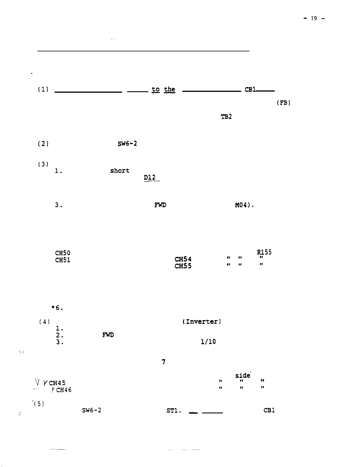
h
COW,JAPAN
SPINDLE
XNTROLl_ER
.model F
Versior,
ConfideTtial:
Some material i?
is
3.00
for
internal use only.
R-SE
chi3
..r-
i .
/+
‘, i
manuai
FR-SE
YiIXT
MAN
BNP-A7237-35A
Page
Front Panel (Fig.
t
:
Hinge Panel (Fig. 2)..................................
3.
General Instructions for Changing FR-SE Card's
Magnetic Sensor
2:
Encoder System FR-SE Spindle Drive (Fig.
6.
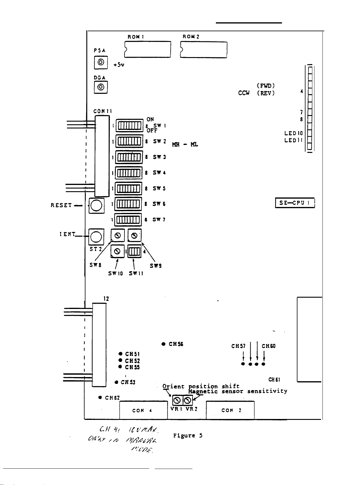
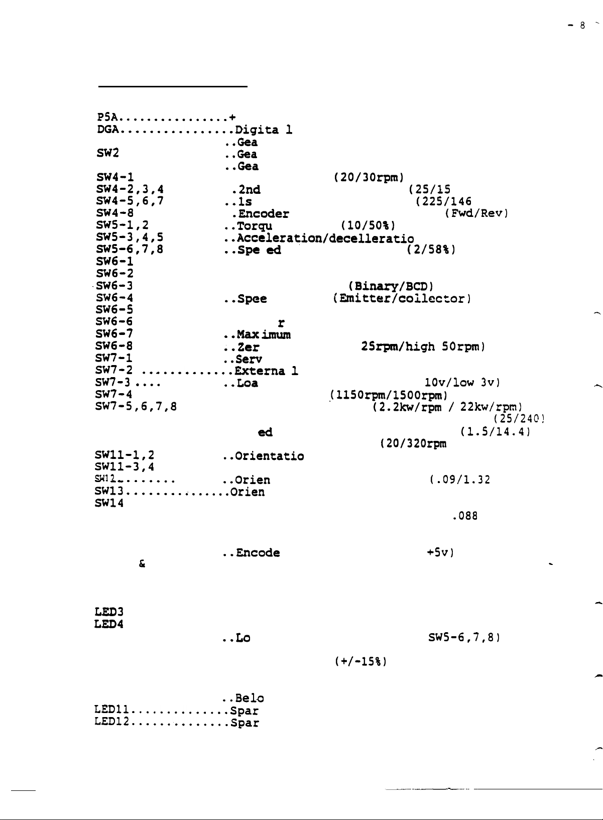
Freqrol SE-CPU1 Card
7.
FR-SE SE-CPU1 Card (Fig.
8.
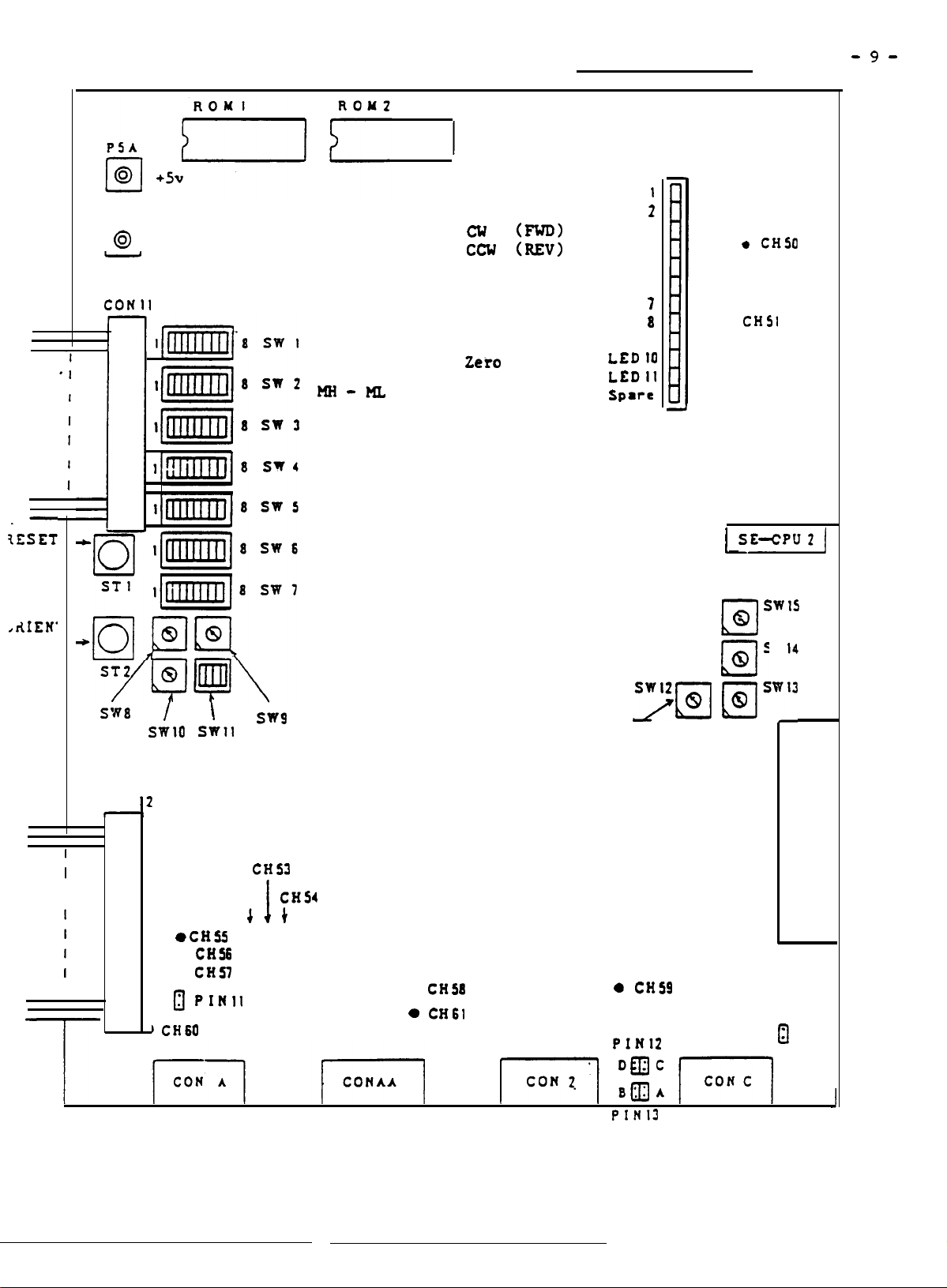
Freqrol SE-CPU2 Card
9.
FR-SE SE-CPU2 Card (Fig. 6)
10.
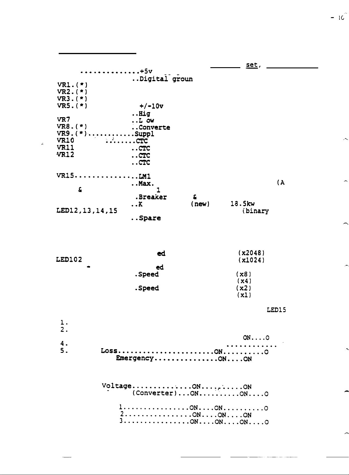
Freqrol SE-IO
FR-SE SE-IO Card (Fig.
11.
General Instructions for Changing FR-SE
12.
13.
Current Transformer Offset Adjustment Procedure......1 3
14.
FR-SE PLG (Tachometer) Diagram
15.
SE Motor Shaft Rotation vs Command
16.
PLG Waveforms
PLG RPM Graph (Fig.
17.
PLG Adjustment
18.
Magnetic Sensor Waveforms C Diagram
19.
20.
Magnetic Sensor Adjustment Procedure.................1 7
21.
FR-SE Base Driver Waveforms (Fig.
22.
Procedure for Checking Base Driver
Maximum Speed Adjustment.............................2 0
23.
Meter Output Adjustment..............................2
24.
FR-SE Converter Output Firing Sequence
25.
26.
FR-SE Inverter Waveforms (Fig.
27.
FR-SE Inverter Waveforms (Fig.
28.
Adjustment of Converter Enable Circuit...............2 5
29.
EPROM Location/Insertion Diagram (Fig.
30.
Instructions for Changing FR-SE EPROM................2 7
31.
FR-SE
32.
Testing Output Transistors, Diode,
33.
FR-SE
34.
FR-SE 7.5 Kw Base
35.
FR-SE 11 Kw Base
36.
FR-SE 15 Kw Base (Fig.
37.
FR-SE 18.5 Kw Base (Fig.
38.
FR-SE 22 Kw Base (Fig.
39.
Blank
40.
FR-SE Basic Diagram
41.
Main Power Circuit (Fig.
42.
Converter Output Circuit (Fig.
43.
Inverter Output Circuit
44.
FFt-SE
45.
Blank Page...........................................4 2
46.
FR-SE Control Block Diagram (Fig.
47.
Circuit Descriptions .................................
48.
Block Diagrams (Fig. 29 - I........................
Base Layout
5.5 Kw Base (Fig.
Page............................................3
Driver C Output Circuit (Fig.
Card...................................1
l)....................:
.............l
2
..... ...3
FR-SE
Spindle Drive
..................................
5)
...........................
...............................
........................
(Fig.
4)
3)
.......
.........
...4
..S
6
7
...8
...9
0
7)............................11
Hinge........1
2
(Fig.8)...............14
(Fig.
(Fig. 9B &
9C)
.......................
lo)..............................1
Procedure.............................1
9A).........14
(Fig.
lOA).......
..14
4
5
11)................18
Waveforms.........1
9
1
(Fig.
(Fig.
(Fig.
(Fig.
13)...................2
14)...................2
15)...........2
16)..........................2
&
Capacitors......2 9
17)
..........................
18)..........................3
.
19)...........................3
20)...........................3
21).........................3
22)...........................3
12).....2
2
3
4
6
8
30
2
3
4
5
1
6
(Fig.
23)........................3
241.........................3
25)...................3
(Fig.
26)
...................
27)..............4
28)................4
7
8
9
1
3
_,’

._
A
it
MITSUBISHI
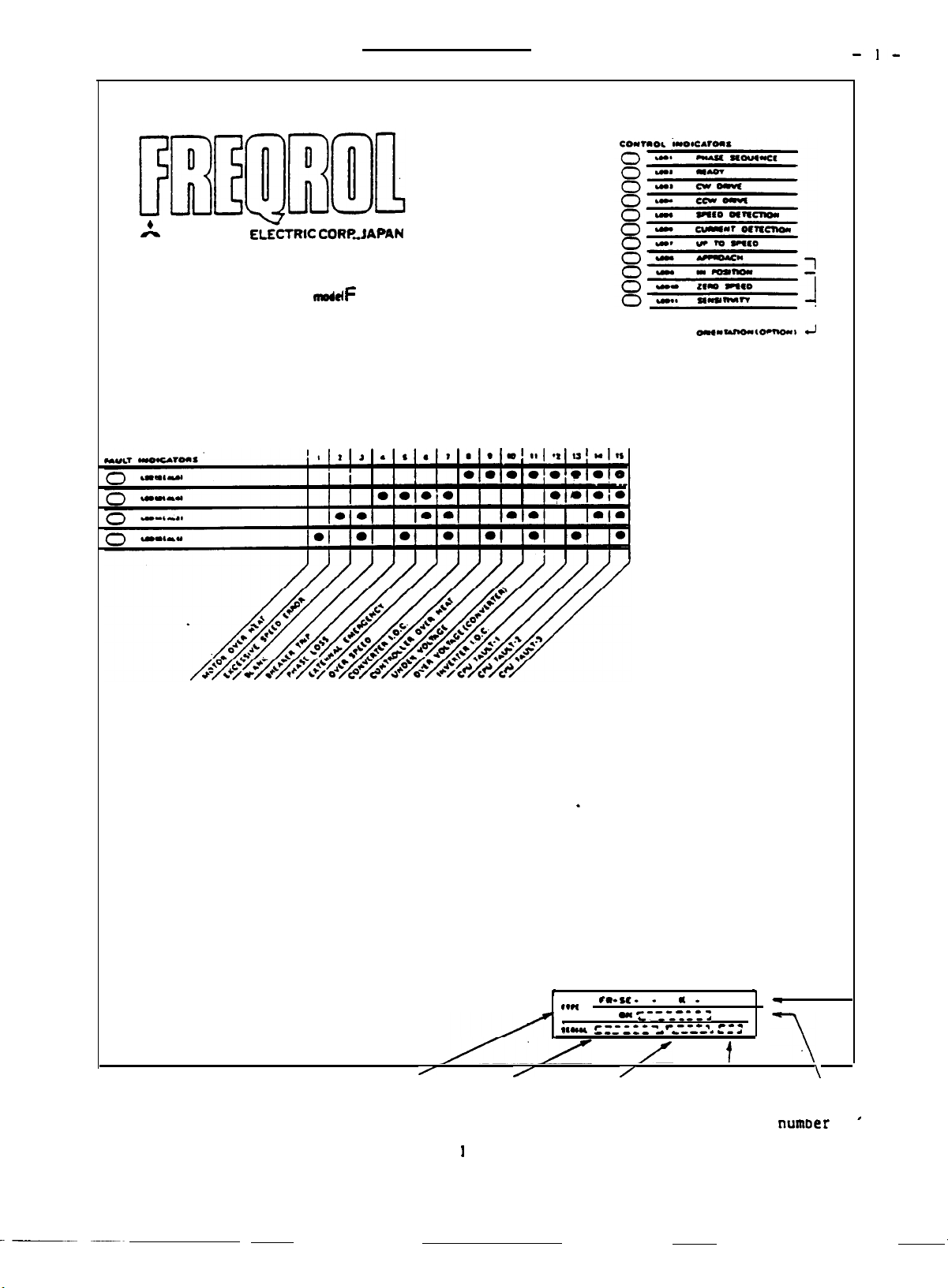
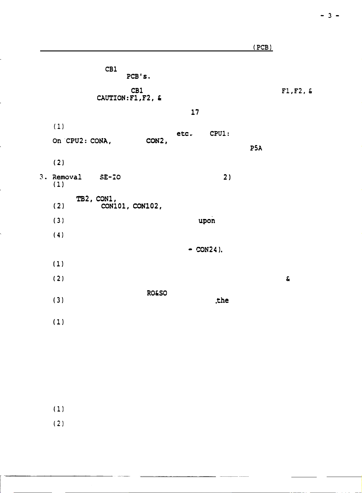
FR-SE Front Panel
ELiklRIC CORF!.JAPAN
AC SPINDLE
CONTROLLER
mod F
R- SE
Note: When exchanging hinge panel the original front panel should
stay with the machine. This is so that the original BN number
will stay with the machine.
The BN number indicates the switch
settings for the spindle drive.
,
-
c-.
b-4
N
f
\
\
/
Nameplate
/
serial
number
I
CO-U..
W”
~-----~
I*- ______
m ------
c,
/
_____d
*
a-
-
p---.
_
B-s.
manufacturing check number
date
numDer
Figure
I
parts list
TYPE
I
or' order
CI
1
’
_-
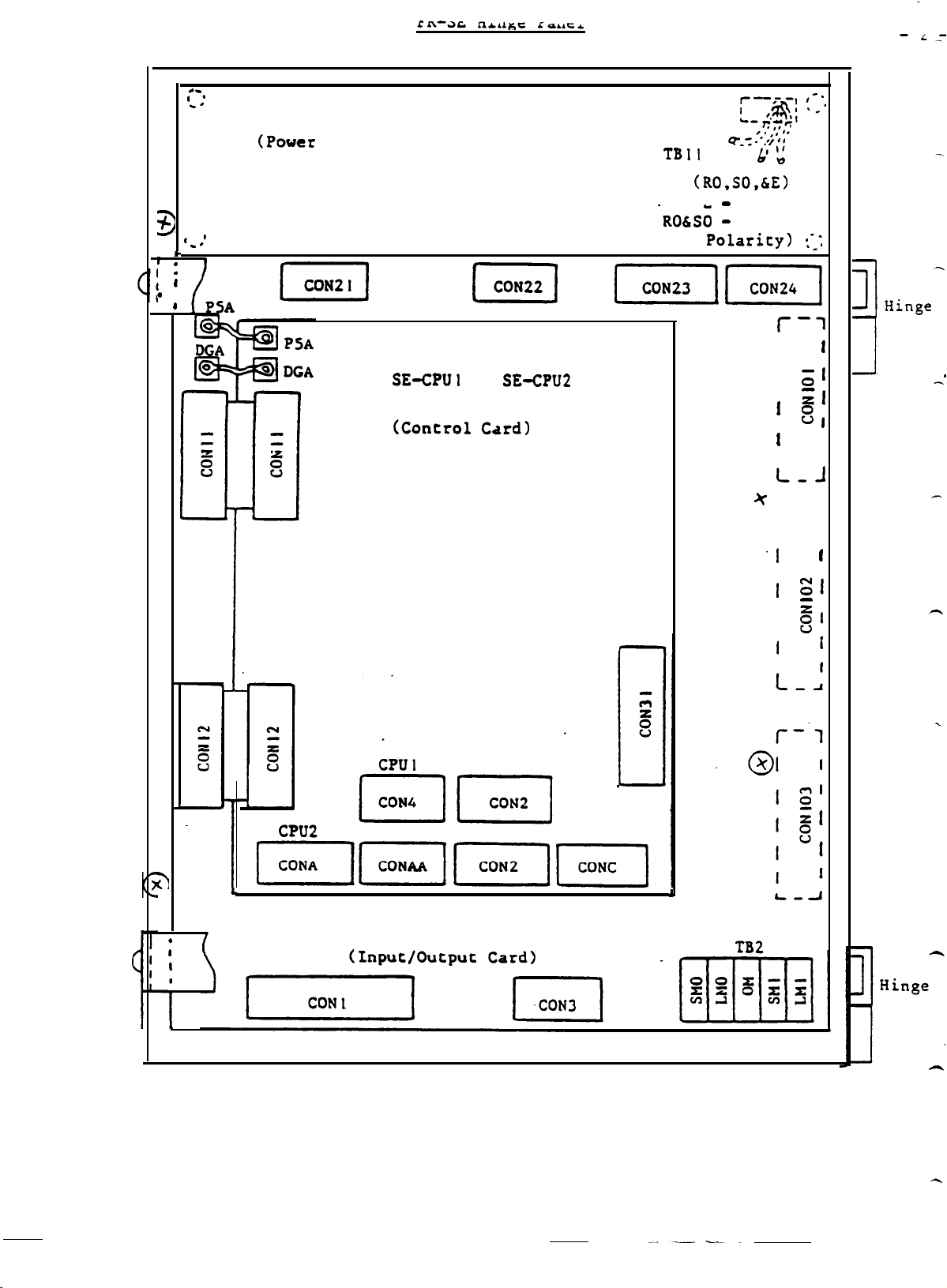
SE-PW
Hinge
5
t t
I
1 ’
*
. .
'_.I
:
8
(Power
Supply)
.
SE-CPU1
(Conctol Card)
or
SE-CPU2
To
'R06SO
TBII
(RO,S~,~E)
-
Green
E
-
White
(No
Polaricy) :l;
0
b:
*
r-1
I
I
’ 8,
’
I
L-1
r-7
.I
1 _
I
1
0’
Zl
I
a
h
81
Hinge
.
;‘
.
,
l
A
SE-IO
Figure 2
b
LB
.A
-3-
General Instructions for Chanqinq FR-SE Card's
1. Remove power from unit.
Note:
Note:
FR-SE
and other
CBl
breaker does not remove power from SE-PW
PCB's.
If Main Breaker
removed by
F3.
CAUTION:Fl,F2, &
CBl
breaker and removal of fuses
(Use Machine Main Breaker)
cannot be
shut off. Power can be
F3 are live at this time. Fuses
(PCB)
Fl,F2, t
are usually located inside of base unit on the line
filter. Refer
to
Figures 17 to 22 (FR-SE Base).
2. Removal of SE-CPU card. (Refer to Fig. 2)
(1)
Remove the connectors for external connection of
orientation detector, PLG,
On'CPU2:
CONA,
CONAA,
CON2i
CON11 and CON12. Unscrew power supply wires
Note: Honda connectors
(2)
Remove the card while
tion spacer claws.
7
_ .
aemoval
(1)
of
After removal
SE-IO
card. (Refer to Fig.
of
the above procedure,
from
(2)
TB2, CONl,
Remove
and CON3
CONlOl, CON102,
have screws
the
remove the load/speed meter wiring
etcc
and
On
CONC. TO SE-IO
CPUl:
CON4 and CON2.
card remove
PSA
and DGA.
and retaining clips.
compressing the
card
installa-
2)
CPU card
of the
connectors according to
I/O card.
and CON103 on the rear of the
hinge panel.
(3)
Remove
the small hinge panel
upon
which the CPU card
was installed.
(4)
Remove the screws fixing the I/O card, and then pull
out the upper guide strongly and pull the I/O card from
the SE-PW connectors. (CON21 -
4. Remove the SE-PW power
(1)
Remove
the CPU card and I/O card according to the
supply.
CON241
,
(Refer to Fig. 2)
above procedure,.
(2)
Remove the three 200 volt
from the terminal
Note:
(31
E is green and
Remove the screws on the back
block located on the base of the unit.
RO&SO
are white with no polarity.
AC
power wires RO,SO, 6 E
of
She
hinge holding the
SE-PW and the remove the SE-PW unit.
5. Assembly of hinge panel.
(1)
Install the
new
cards
in the reverse
order of the re-
moval procedure.
Important Note:
After replacement,
confirm that all
screws
and connectors are tight and correct. Also
verify positive insertion of the connectors.
Applying Power:
1. After replacement,
all specific adjustment procedures
should be observed. Especially current transformer
offsets,
meter calibration,
and
orientation.
2. Verify that EPROM's and switch settings are correct.
3. Optional:
Verify that base driver waveforms are correct.
4. Verify spindle operation:
(1)
Confirm full speed range in each gear
reverse.
(2)
Confirm orient
operation).
Verify alignment before attempting ATC.
operation in each gear (Including ATC
forward and
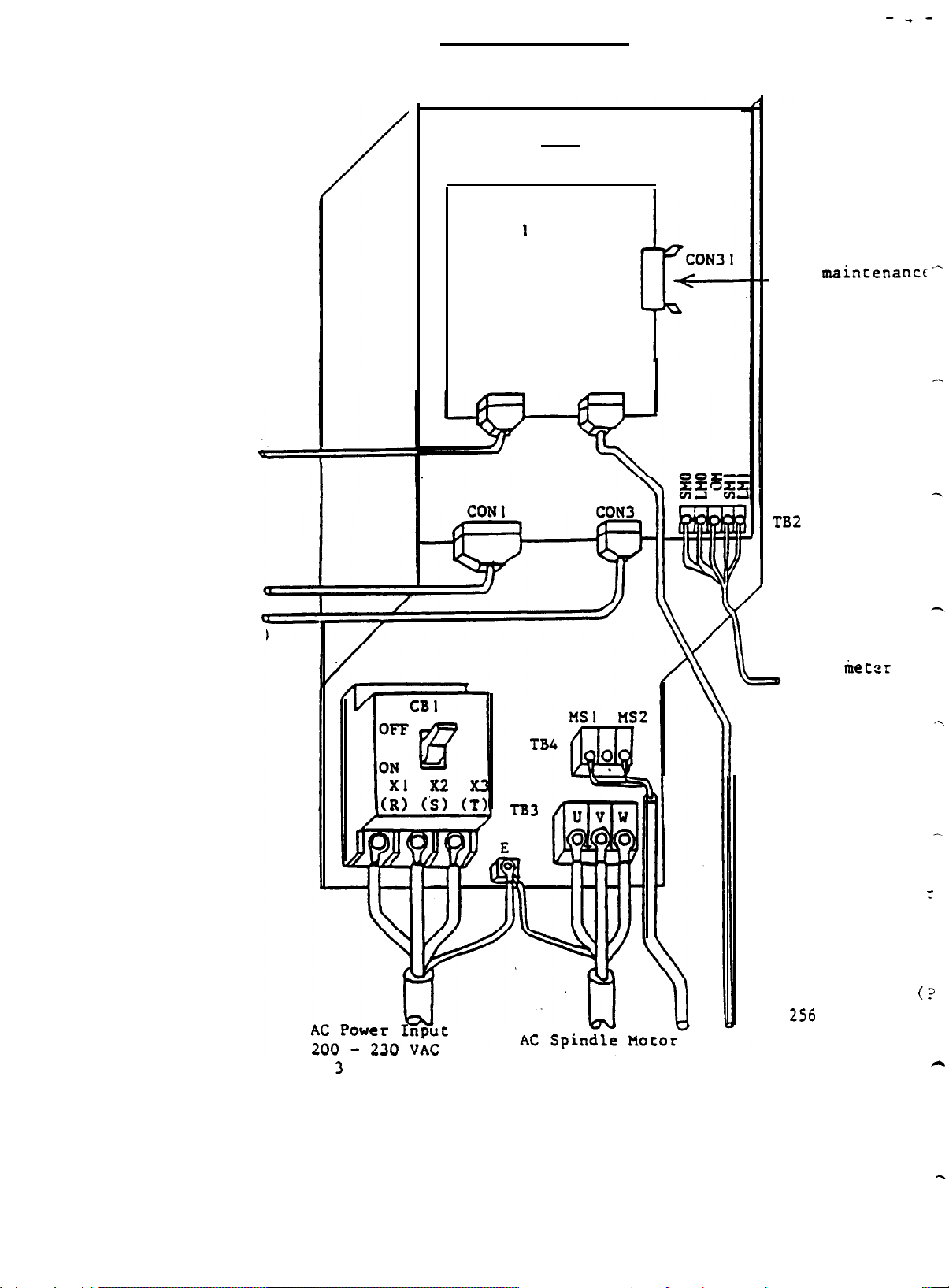
FR-SE Spindle Drive
--t-
Magnetic sensor system
Orientation position
Magnetic
sensor
input
with single point orientation
FR-SE-2-
SE-IO
SE-CPU
I
CON4
-K-F
CON2
unit
For
panel
maintenance"
Sequence
circuit
(Input/output)
Load
Speed meter
Note:
256 pulses/motor
Pulse generator
256
Overheat detection
tieccr
PLG is 2
pulses
pha
(?
r
3
Phase
Figure 3
Motor
blower
A
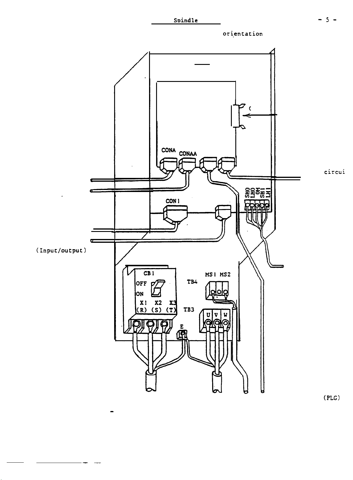
FR-SE
Sbindle
Drive
-5-
Encoder system with multiple point
Orientation position
2 phase 1024 pulse/rev.
Encoder input
Encoder output
to CNC
’
8
6
FR-SE-2-
SE-IO
SE-CPU2
CONA CoNAA
-K-A
CON2
ori.entation
CON31
I=
CONC
CON3
unit
_
For maintenance
panel
Sequence
(Orientation posit
data)
TB2
circui
Sequence
circuit
(Input/output)
a
0
AC Power Input
200
-
230 VAC
AC Spindle Motor
Note: PLG is 2 phas
256
Overheat detection
pulse generator
Motor blower
Load meter
Speed meter
pulses/motor re
(PLG)
-_
3 Phase
Figure 4
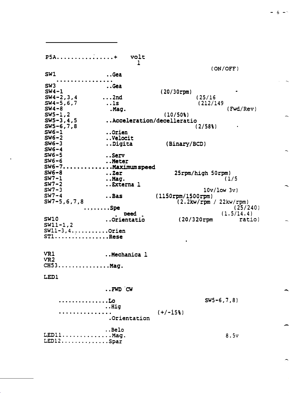
Freqrol SE-CPU1 Card
I
Refer to Figure 5 for location.
PSA................+
DGA
.............. ..Digita 1 ground
SW1
..............
SW2
.................
SW3 ..............
sw4-1
SW402,3,4
SW4-5,6,7
SW408
sws-1,2
sws-3,4,5
SWS-6,7,8
SW601
SW602
SW603
SW604
SW605
SW6-6
SW60?
SW6-8
sw7-1
SW7-2
sw7-3
sw7-4
SW7-5,6,7,8
SW8
SW9
SW10
SWll-1,2
............
.......
........
...........
..........
........ ..Acceleration/decelleratio
........
............
............
............
............
............
............
..............
............
............
............
............
............
......
........
.............
.............
..?.....Spe
. ..S
......... ..Orientatio n
SWll-3.4...........0rien
STl......l.........Rese
ST2
..............
5
volt
supply
..Gea
r ratio H
Gear ratio
..Gea
r ratio L
..Cree p speed
...2nd
..ls
...Mag.
deceleration point
t deceleration point
Sensor mounting direction
..Torqu e limit
M
(20/30rpm)
(lo/SO%)
..Spe ed detection range
..Orien
..Velocit
..Digita
t
(Normal/test)
.y loop (Closed/open)
1 input
(Binary/BCD)
..Spee d input (Emitter/collector)
..Serv
.-Meter
..Zer
..Mag.
..Externa 1
o rigidity (High/low)
calibration (Off/On)
.
IUxmum speed
(Low/high)
o speed (Low
Sensor orient in-position
E-Stop alarm display (On/Off)
..Loa d meter output (High
..Bas
e speed
(1150rpm/l500rpm)
..Moto r size/type
ed loop proportional constant
peed
loop integral constant
..O&entatib
n
speed
direction select
t stop
servo rigidity
t
..Orien t test
Switch:
(25/16
(.ON/OFF)
degree)
(212/149
degree)
.
(Fwd/Rev)
also external input
n time constant
(2/58%)
.
ZSrpm/high 50rpm)
(l/S
deg.)
lOv/low 3~)
(2.2kw/rpm / 22kw/rpm)
(25/240)
(l-5/14.4)
(20/320rpm
.
/gear
ratio)
4
VRl
..............
VR2
..............
CH53...............Mag.
LED1
LED2
LED3
L&D4
LED5
LED6
LED7
.............
............. ..Read y condition
.............
...............
...............L~
.............
...............
LED8 ..............
LED9
...............
LED10 ............
LEDll..............Mag.
LEDlZ..............Spar
..Mechanica 1
orient position shift
..Mag. Sensor sensitivity adjust
Sensor input
..A C Power phase identification
..I= 'CW
rotation command
. CCW rotation command
w speed detection (See
..Hig
h motor current (110%)
Up to speed
.Orientation
(+/-i5%)
approach
SWS-6,7,8)
In position orient stop
..Belo
w zero speed
Sensor signal level above
8.5~
e
4
5-J
--
+sv
;A
Digital ground
>N I I
FR-SE SE-CPU1 Card
Gear Ratio H
Gear Ratio
ml-ML
Gear Ratio L
Phase
Ready
cw
ccw (REV)
Speed
Current
Up
Approach
In Position
Zero Speed
Hag. Sensor
Spare
(FWD)
CO
Speed
LED I
LED 2
L&D 3
LED
4
LED 5
LED 6
LED
7
LED
6
LED 9
LED10
LED11
Spare
-7-
RESET -
OR
1 ENT_
TEST
iol
ST 1
CON
1
Test, Etc.
CH58 CH59
1
SE--CP'Jl
l
CON31
_.
CH50
j
l
cn54
l
CX61
Freqrol
SE-CPU2 Card
Refer
PSA................+
to Figure 6 for location.
5 volt supply
DGA................Digita 1
...
.
SW1
..............
SW2
SW3
..............
sw4-1
SW4-2.3.4
SW4-5,6,7
sw4-a
sws-1,2
sws-3,4,5
SWS-6,7,8
SW601
SW602
.SW6-3
SW604
SW6-5
SW6-6
SW607
SW6-8
sw7-1
SW702
sw7-3 ..*.
sw7-4
sw7-5,6,7,8
SW8
..............
SW9
..............
SW10
SWll-1,2
SWll-3.4
SW12
. .
sw13..::::.
SW14
SW15
ST1
..............
ST2
..............
PIN11
PIN12 & PIN13
SPARE PIN
LED1
LED2
LED3
LED4
LED5
LED6
LED7
LED8
LED9
LED10
LEDll..............Spar
LEDlZ..............Spar
..........
............
.........
........
.............
..........
..Cea
..Gea
..Cea
..Cree p speed
..ls
..Torgu
r
r
r ratio L
.2nd
deceleration point
t deceleration
.Encoder
e limit
........ ..Acceleration/decelleratio
........ ..Spe ed
............ ..Orien t (Normal/test)
............
............
............
............
............
.........
............
............
.
..-..........Externa 1
........
............
......
..Velocit y loop (Closed/open)
..Digita 1 input
..Spce
..Positio n input (Emitter/collector)
d input
..Mete
...
..Max
..Zer
..Serv
..Loa
..Bas e
intum
o
o rigidity (High/low)
d meter
..Moto r size/type
..Spee d loop proportional constant
..Spe
.............
.........
....
.....
.......
..Orientatio n speed
..Orientatio
..Orien t stop servo rigidity
..Orien
........Orien
.............
.............
..Orien t position shift (Medium 1.4 deg.1
..Orien t position shift (Fine
ed
loop
t in-position range
t position shift (Course 22.5 deg.)
..Rese t
..Orien t test
............
...
.....
.............
............. ..Read y condition
...............
...............
.............
........
.......
.....
......
..Encode
....
..CON C Orient position input level select
..Extr a jumper
..A C Power
. CW rotation command
. CCW rotation command
..Lo
w speed detection (See
..Hig h motor current (110%)
..U p to Speed
............. ..Orientatio n approach
...............
............
In position orient stop.
..Belo
w zero speed
e
e
Switch: (ON/OFF)
ground
ratio H
ratio
mounting
M
(20/30rpm)
point
direction
(lo/SO%)
(25/Z
(225/146
also
degree)
degree)
(Fwd/Rev)
external input
n time constant
detection range
(Binary/BCD)
(&nitter/coilcctor)
r
calibration (Off/On)
speed (Low/high)
speed
(Low
E-Stop alarm display (On/Off)
ZSrpm/high 50rpm)
output (High
speed
~1150rpm/1500rpm)
(2/58%)
lOv/low 3~)
(2.2kw/rpm / 22kw/rpn)
integral constant
(20/320rpm
(1.5/14.4)
/gear ratio)
n direction select
(.09/1.32
-088
deg.)
r power
phase identification
supply (ON
strap
+Sv)
SWS-6,7,8)
(+/-15%)
(25/24@!
degree)
-
DGA
@
Digital ground
rl
CON11
Gear Ratio H
Gear Ratio
HH
-uL
Gear Ratio L
Phase
Ready
CM
(FWD)
CCIJ (REV)
Speed
Current
Up to Speed
Approach
In Position
Zeta
Speed
Spare
Spore
FR-SE SE-CPU2 Card
LED
I
LED
2
LED 3
LED4
LED 5
LED 6
LED
7
LED
LED 9
LED10
LED11
fp8rt
6
. CHSI
t CHSII
-
9
-
1
,rLIEN’
TEST
SW0
CON
SW10
1
0 CHSS
l
.
Q
’ CH60
\
SW11
CHS6
CHSI
PIN11
SW9
CH53
CH52
I
A I
l 00
Test, Etc.
CHS4
.
CHSS
0 CH61
1 SE--cPU2]
0
Orient Position
Shift
?=I
Kl
8
Q_
.5:'3
In Position Range
CON31
0
CH59
l
CH62
PIN12
SW IS
SW
I4
SPARE
PIN
0
T
PIN13
Figure 6
Freqrol SE-IO Card
-
IC’
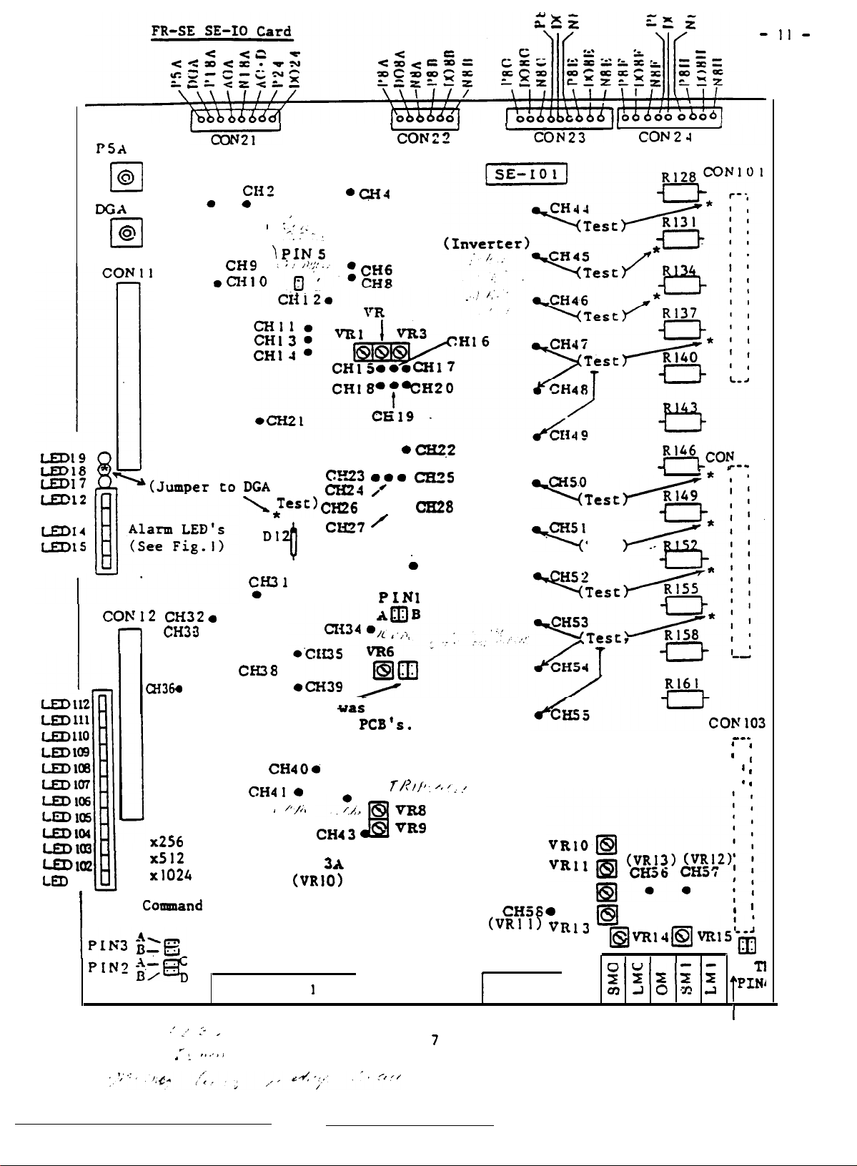
Refer to Figure 7 for location.(*) Factory
PSA..
DGA
VRl.(*) ............
vR2.t*1
vR3.(*)
VRs.(*)
VR6
VR7
VR8.(*)
VR9.(*),
VRlO
L
VRll
VR12
vR13
VR14
VRlS
PIN1 .............
PIN2 6 PIN3
PIN4
PINS
LED12,13,14,15
LED16
LED17
LED18
LED19
LED20
LED101
LED102
LED103
LED109
LED110
LED111
LED112
. . . . . . . . . . . . . .
..............
............
............
............
..............
..............
..........
..,....,.....~uppl
.....
.
.
;./......CTC
.............
.............
.............
......
.............
.......
......
..............
.............
...
....
........
+sv
supply
.-Digital-g%oun
.
Phase
current command zero adjust
d
. Phase current command zero adjust
. Phase current. command zero adjust
+/-10~
..Hig
..L w
..Converte
Reference adjust (not used)
h over-speed level adjust
over-speed level adjust (not used)
r voltage gain adjust
y voltage peak value gain adjust
1 Converter offset adjust
..CTC
..CTC
..cTC
..SM 1
..M
..Mu.
2 fnverter offset adjust
4 V Phase motor current offset adjust
3 U Phase motor current offset adjust
Speed
1
Load meter output adjust
meter output adjust
speed or Over-speed select (A used)
..CON I Digital speed input level select
.Breaker
..E
w setting
trip 8 overheat-alarm disable
(new)
OFF
..Driv e alarm indicators
.-Spare
............ ..Unde r voltage indicator
............ ..Converte r regeneration indicator
............
............
...........
...........
-
LED108
............
...........
............
...........
..Bas e transistor cut-off indicator
..Converte r voltage charging
..Spe ed command display
..Spee d command display
..
..Spe ed command display
.Speed
command display
..Spee d command display
.Speed
command display
..Spee d command display
set,
18.Skw
or larger
ibinary
(x2048)
(x1024)
(x8)
1x4)
(x2)
(xl)
don't change.
,.
output)
.--.
Spindle Alarms:
Motor Over Heat
;:
Excessive Speed Error..................ON
3.
Blank
..................................
Breaker Trip
Z:
Phase
6 .-
External
7.
Over Speed
8.
Converter I.O.C............ON
9.
Controller Over Heat.......ON................O N
10.
Under
11.
Over Voltage
12.
13.
14.
15.
Inverter I.O.C.............ON....ON
CPU Fault
CPU Fault
CPU Fault
Loss.......................ON..........O
Emergency...............ON....ON
.....................
Voltage..........;...ON....,;.....ON
l................ON....ON..........O
Z................ON....ON....ON
3................ON....ON....ON....O
LED12 LED13 LED14
AL8 AL4 AL2
..............................
LEDlS
AL1
ON
......
.....................
ON
ON....0
.............
N
N
......
..ON....ON....O N
..................
......
(Converter)...ON.....'.....ON....O
N
............
N
......
N
-
II
-
La?12
LED13
LED14
LED15
SPARE
Lm1u3
ml02
Lm
101
PSA
0
cl
DciA
62
cl
CON12
n
Speed
I
PIN2 2.7::
CHI CH2 .
0
0
. CH9
0 cxi I 0
CH32.
CIi33
l
Q-i360 l CIi37
Xl
x2
x4
X8
x16
x32
x64
x128
x256
x512
x1024
x2048
Counnand
LED’s
%
.’
’
_’ : ,
r
I : II.‘,,
CH3
I
I :‘<.
r, -,
1PL’NS
DGA
for
\ zest) Cm6
Dl2
cH31
0
CH38
l
b
VR7
l
Cx23.0.
-4
cfi27 ’
CH29 .
on new
CH40L
CH41 0
/ /‘/,a
CH4 2
CH4 3A .
(VR 10)
CON
I
1
l
CHS
.CH4
QI7
VR
,’
l l
CON2
2
2
. cx?z
-5
o
CK28
(Converter)
i
CH30
PIN1
ua;
replaced by SPARE
PCB’s.
T/?/p: ‘.
fi
1
Figure
7
J
CON23
.I
CH58.
(VRI I> VR13
CON 3
VR12
CON24
MCON
I
Test
LED200 f
@Jo.
m
@JVFM(cJ VRG-i
00
IZZI’I
Q) J 0 .-Yz OJ
TB2.
102
I---
‘*
SW_
1
I
’
I
:
i;
I I
. .
-
FB
7.-l
PIN
I
I
Breaker tria
alarm dis
- 12 -
General
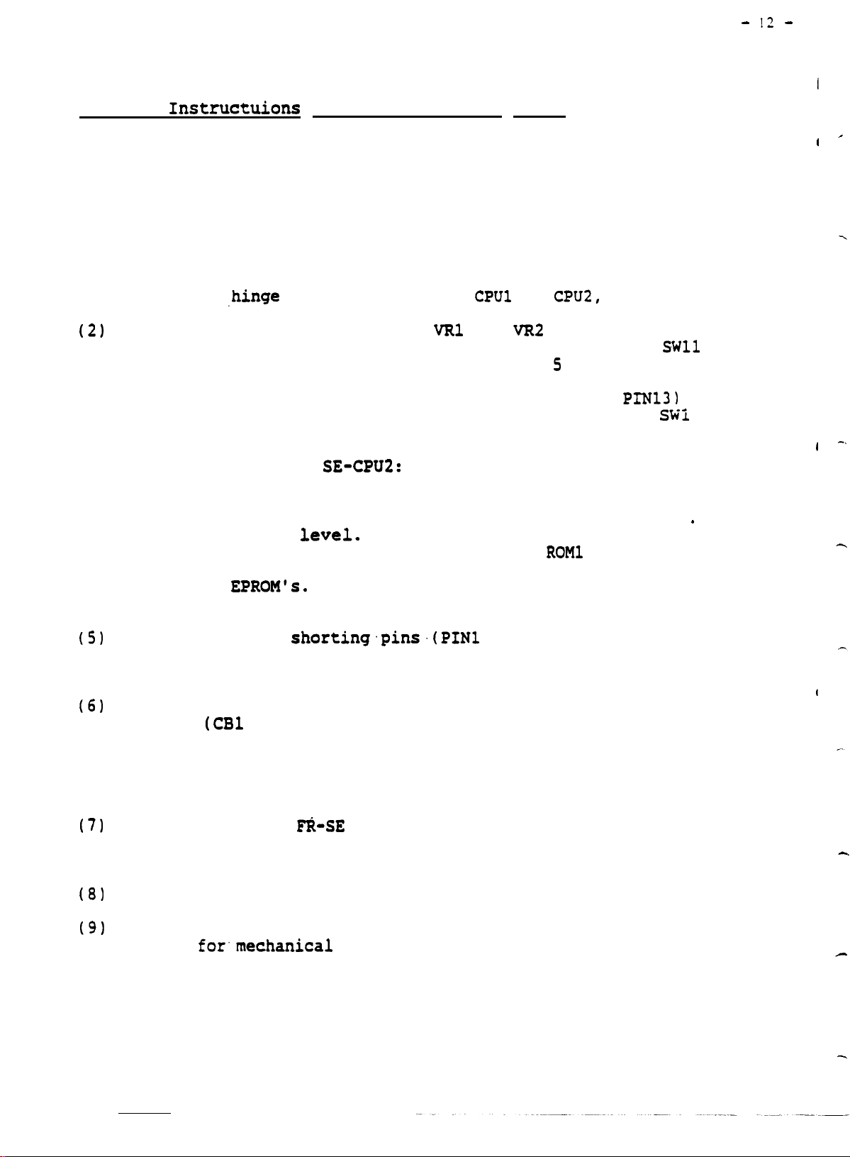
Before exchanging the
Instructuions
for Changing FR-SE Hinge
FR-SE hinge panel please confirm the
following:
(1) Remove the
later installation
original hinge cover panel and keep it for
on
the new hinge. This maintains the
original BN number on the spindle drive. The BN number tells
the service
the controller's
Note:
(2)
original card.
Spindle
SE-CPU1 Card:
the same as the original card. Refer to Fig.
(3) SE-CPU2
same as the original
through SW15 the same
(4) EPROM's SE-CPU1 and
engineer the
ratings.
,hinge
Card: Set shorting
will have either
Set adjustments
Set
dip
card.
settings.
Refer to Figure 1 if necessary.
and rotary switches SW1 through
pins (PIN11 through
Set dip and rotary switches
as
the original
SE-CPUZ:
Verify that numbers on the
of
the pins, switches and
CPU1
VR1
or
and
CPUZ,
VR2
the same as the
not both.
SW11
5
for locations.
PIN131
SWi
card.
Refer to Fig. 6.
the
new EPROM labels match the original EPROM. Newer versions of
software EPROM's will have a higher number or letter on the
label, which is
verify ERPOM version
original EPROM's in the new CPU card if the
sockets are empty.
in installing
ok. If unsure please
level.
Use
EPROM's.
care
Do not
Please
in removing EPROM's and caution
install upside down, as this
call Mitsubishi and
.
remove and install the
ROM1
and ROM2
will damage the EPROM. Refer to Figure 15 for detail.
I _
.
4
(5)
SE-IO Card: Set
same as the original card.
than those specified in the instructions. Refer to
(6)
Optional:
full power
Test base driver waveforms'before restoring
(CBl
OFF).
output transistors were
being damaged.
Diode,
and Capacitor.
Refer also to Testing Output Transistors,
shorting.pins,(PfNl
through PINS) the
Do not make any adjustments other
Fig.
7.
This test should be performed if
damaged
and replaced or suspected of
See Procedure for Checking Base Driver
Waveforms.
(7)
After installing
offsets for
Transformer
(81
Confirm
(9)
Confirm
require it
the DC current transformers. Refer to Current
Offset
full speed range in all gears FWD and REV.
alignment of spindle at orient in machines that
for.mechanical
F&SE
hinge panel please readjust the
Adjustment Procedure.
operations such as ATC. This may
involve measuring the spindle orient position relative to
axis movement
as specified by the machine manufacturer.
Confirm orientation in each gear. (Including ATC.)
Current Transformer Offset Adjustment Procedure FR-SE
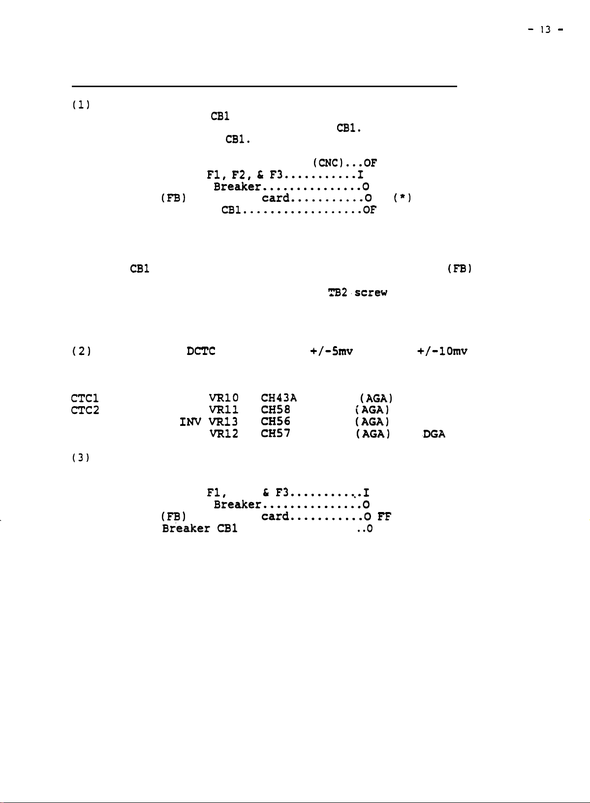
(1)
Offsets should be adjusted with zero current. This is
done, by switching
the BREAKER TRIP alarm(*) caused by
or 4 for location of
CBl
breaker
CBl.
(Note that up is OFF.)
OFF
on FR-SE and disabling
CBl.
Refer to Fig. 3
- 13 -
Note:
Note(*):
Computer Numerical Control
FR-SE Fuses
Machine Main
Pin 4
(FBI
FR-SE Breaker
Fl, F2, & F3...........1
Breaker...............0
on SE-IO
card...........0
CBl..................OF
(CNC)...OF
F
N (GOOD)
N
N
F
(*I
It may not be necessary to disable the breaker trip
alarm to complete current transformer adjustments.
Disable
CBl
breaker trip alarm by inserting jumper
(FBI
on
Pin 4 of SE-IO PCS. This is located on the lower right corner
of the PCB and to the right
to lower right corner
of
Figure 7.A SPARE jumper strap can
of
the
TB2-screw
terminal. Refer
usually be found on the SE-CPU or SE-IO printed circuit
boards.
(2)
Adjust all
acceptable).
DCTC
offsets
to Ov
+/-Smv
(Note:
+/-1Omv
is
Refer to bottom of Fig. 7 for location of ad-
justments and check points.
CTCl
Converter
CTC2
Inverter
CTC3 U Phase
CTC4 V Phase INV
VRlO
VRll
INV VR13
VR12
CH43A
CH58
to CH2
CH56
to CH2
CH57
to CH2
to CH2
(AGA)
(AGA)
(AGA)
(AGA)
or DGA for Ov.
or DGA for Ov.
or
or DGA for Ov.
.DGA
for Ov.
(3)
After adjustment return spindle drive to normal settings.
Note: CNC
................................
FR-SE Fuses
Machine Main
Pin 4
FR-SE
(FB)
Bleaker CBl
Fl,
F2, L
Breaker...............0
on SE-IO
................
F3.........,.1
card...........0 FF
OFF
N
N
..O
N
Refer to Figures 17 to 22 (FR-SE Base) for location of fuses.
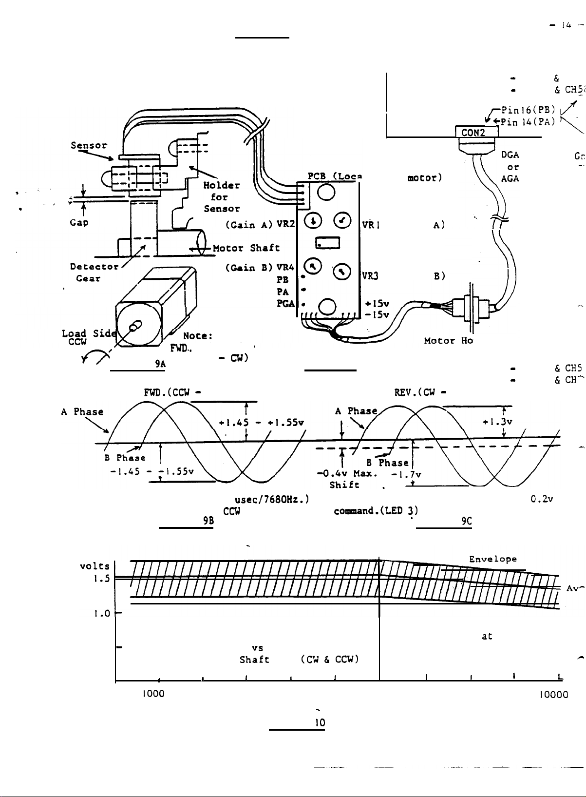
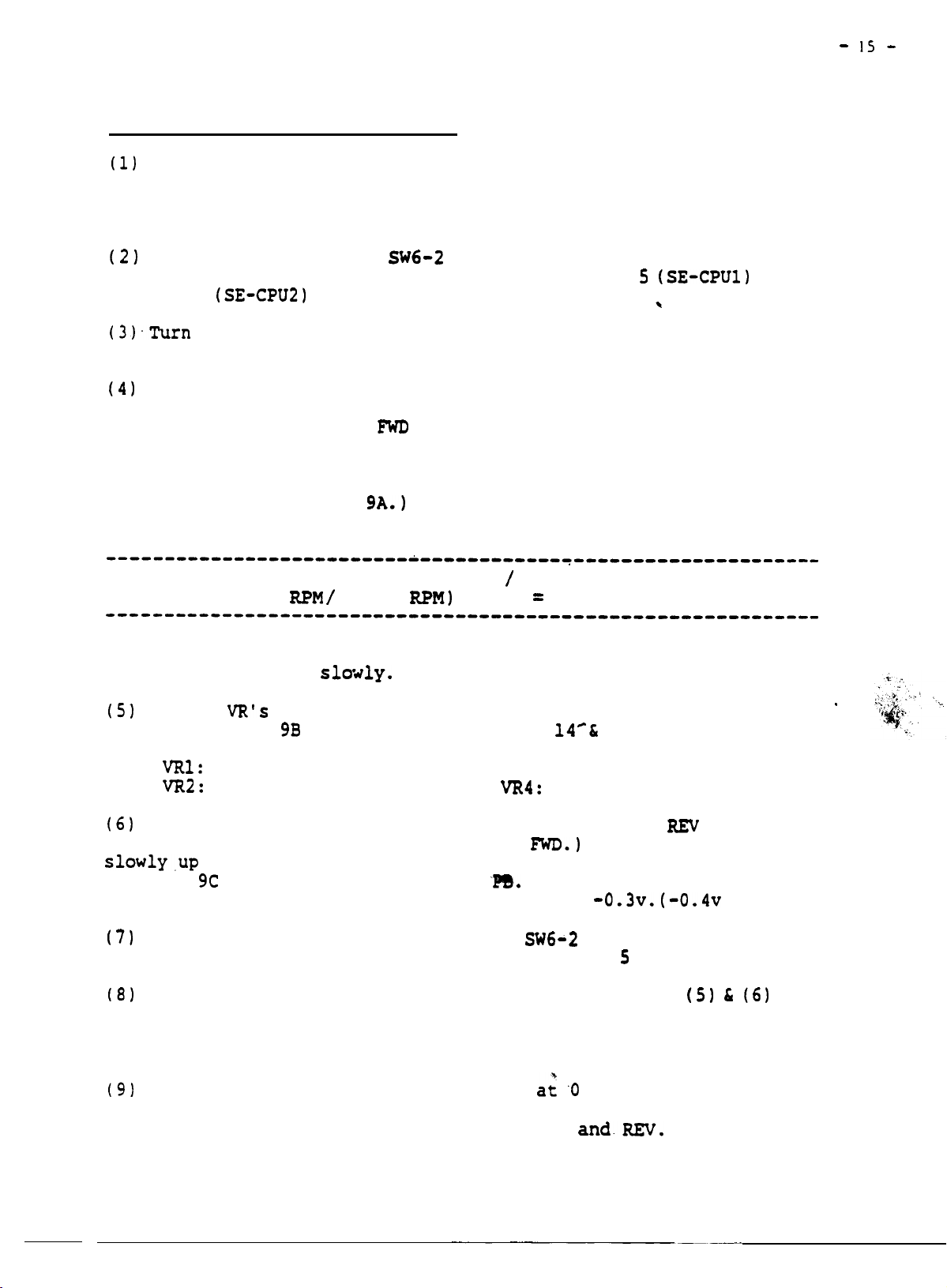
Output is
of the
motor
FR-SE PLC
256
pulses per revolution
shaft.
-
I& --
Amplified signals C?'
I
SE-CPU
Card
[CON2 1
PA -CH59
PB
-
CH62 &
rPinl6cPB)
LC+Pin
14(PA)
&
CH6
CHS_i
Lf
ted in
VRI
(Offset
(Signal
motor)
A)
Cr.
_.
\
VR3
(Offset
(Signal Ground
B)
4
FWD..
/
0
Figure
FWD.(CCW -
9A
Direction
(LED3-
LED3 ON
Cla>
Figure 8
REV.(CW -
using
Amplified signals
LED4 ON)
Connector
PA
PB
CH60 &
-
CH57 h
-
CP
CH5
CH-
Motor
Note: Motor shaft rotates
Shaft 1800 RPM (130.2
Figure
Peak
0.5
-
I
IO00
Motor Shaft RPM
9B
PA 6
Motor
1
2000
CCW
PB
Peak Output Volts
3000
usec/7680Hz.)
on CW or FWD.
Shlit
RPM
I
Figure
1
4000
(CW & CCW)
5000 6000
z
IO
Peak values
command.(LED 3)
I
.
Figure
7000
shown are
9C
Confirm output is in
envelope ac maximum
motor RPM.
I
I
8000
9000
0.2~
I
10000
shi.
*
L
- I5 -
PLG
Adjustment Procedure FR-SE
(1)
Normally PLG adjustment is not necessary. The PLG should
be adjusted in open loop to prevent the spindle drive from
responding to PLG signal loss while adjustments are made.
Caution:
(2)
With the CNC
(Reset) on the SE-CPU card. Refer to Figure
Figure 6
In open loop sudden speed changes can cause damage.
OFF. Set
(SE-CPU21
for location.
SW602
OFF
(Open loop) and press ST1
5 (SE-CPU11
and
\
(3).Turn
CW on the FR-SE is ON.
(4)
Caution: Increase and decrease motor speed slowly in open
loop or damage may occur.
1800 RPM slowly in the
vs gear range.
the CNC ON.
Make RPM adjustments manually if possible.
Command the spindle FWD and confirm LED3
If not command REV instead.
Bring the spindle motor up to about
FWD
direction. See note on command RPM
Note: This should be actual motor shaft RPM in CCW direction.
(Refer to
commanded
Figure 9A.l
RPM
should be compensated or else the spindle
If the machine has gears, the
motor will be at an RPM greater than 1800 RPM.
~-~~~~~~~~~~-~~~~~rr~~~~~~~~~~~~~~~~~~~~~~~~~~~~~~~~~~~~~~~~~
Example: (Max. RPM for gear range / Max. motor RPM) x 1800
(4800
RPM /
6000
RPM1
x
1800 = 1440 Command RPM
---------~-------------~~~~~~~~~~~~~~~~~~~~~~~~~~~~~~~~~~~~~~
Note:
(5)
forms in
If the CNC has a spindle override be aware
setting.
up and down
Adjust
VR's
Figure
It can also be used to bring the motor speed
slc~ly.
located on PCB in motor to obtain the wave-
9B
at PA and PB or Pin
14'&
16 of CON2. Refer
of
its
’
to Figure 8 for locations.
VRl:
Offset for A Phase
VR2:
Gain for A Phase
VR3: Offset for B Phase
VR4:
Gain for B Phase
(6)
Slow spindle to zero speed.
ify LED4 CCW is ON.
slowly.up
in Fig.
to about 1800 RPM and confirm that the waveforms
9C
are present at PA and
(If not command
rotating CW the output could shift up to
(7)
Slow spindle to zero speed.
and press ST1 on SE-CPU card. Refer to Fig.
(8)
'If the correct output cannot be obtained in
Command spindle
FWD.)
Bring the spindle
'PB.
When the motor shaft is
-O.~V.(-0.4~
Set
SW602
ON (Closed loop)
RE'V
and ver-
max.)
5
or Fig. 6.
(5) C (6)
it
may be necessary to adjust the gap between the sensor and the
detection gear. Refer to Fig. 8 and the FR-SE Maintenance
Manual. Then repeat adjustment procedure as necessary.
(9)
Check PA and PB output waveforms a; '0 to Max.
RPM in FWD
and REV to conf-irm that they are within the envelope shown in
Figure 10.
Specifically Max.
RPM in FWD
and.REV.
Motor Speed
Sensor MS
signal
Sensor LS
signal
Magnetic Sensor
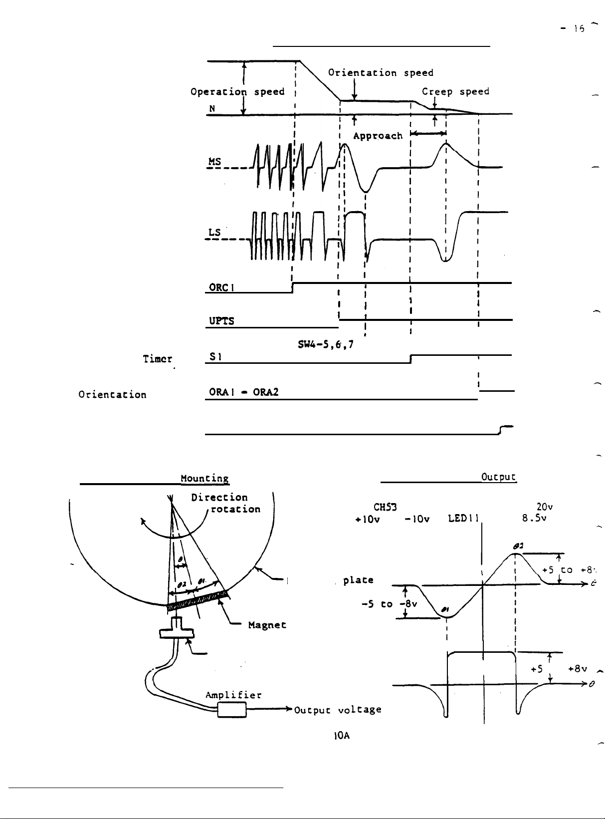
Orient
Timing Chart
-
15-
Oriencacion Command
Speed Arrival
Slow
(software)
Orientation
In Position
Magnetic
Down
Sensor
Timer
.
Finish
Flouncing.
Direction
ORCI
urns
S1
ORAl
LED9
- oRA
of
I
sIa4-5,6,7
Setting
\
Mount
ing
8
I
I
I
I
I
I
I
I
I.
60-95 ms
At
CH53
+lOv
to
MS signal
'P
I
1
I
I
I
1
I
I
I
I
I
I
1
1
I
I
I
I
Magnetic Sensor
Output
the output should
LED11
-1ov
ON at
62
be
8.5
2Ov
p
p-p.
-.
7K
Detection sensor
Figure
IOA
LS
signal
Ltage
I
F
.<_
I
I
+5
CO
+av
_
- 17 -
Magnetic.Sensor
Note :
If
VR1
when a new hinge is installed,
necessary.
is replaced
(1)
Refer to FR-SE Maintenance Manual for information on
Adjustment Procedure SE-CPU1
and VR2 are set the same as the original hinge
adjustment is
Adjustment would be necessary if magnet
or
the gap is adjusted.
probally
not
or
sensor
mounting magnet, sensor, and amplifier. Be sure gap, magnet,
and sensor positioning meet specifications if the following
adjustments do not work properly.
Note:
Do not attempt tool change with ATC until- all adjust-
ments are made and physical alignment is checked.
(2)
Record the position
speed setting) for later use.
(60 rpm)
and set dip switch
press ST1 (Reset). Refer to Fig.
of
rotary switch SW10 (Orientation
Then set SW10 to position 2
SW601
to
OFF
(Orient test). Then
S
or Fig. 6 for loactions.
Note: -Adjustments of magnetic sensor output should be made at
spindle
(3)
Turn
RPM's
of 80 RPM or less.
VR2
(Sensitivity) fully counter clockwise. Refer to
Fig. 5 or Fig. 6 for location of adjustments and check point.
Method 1 (Oscilloscope):
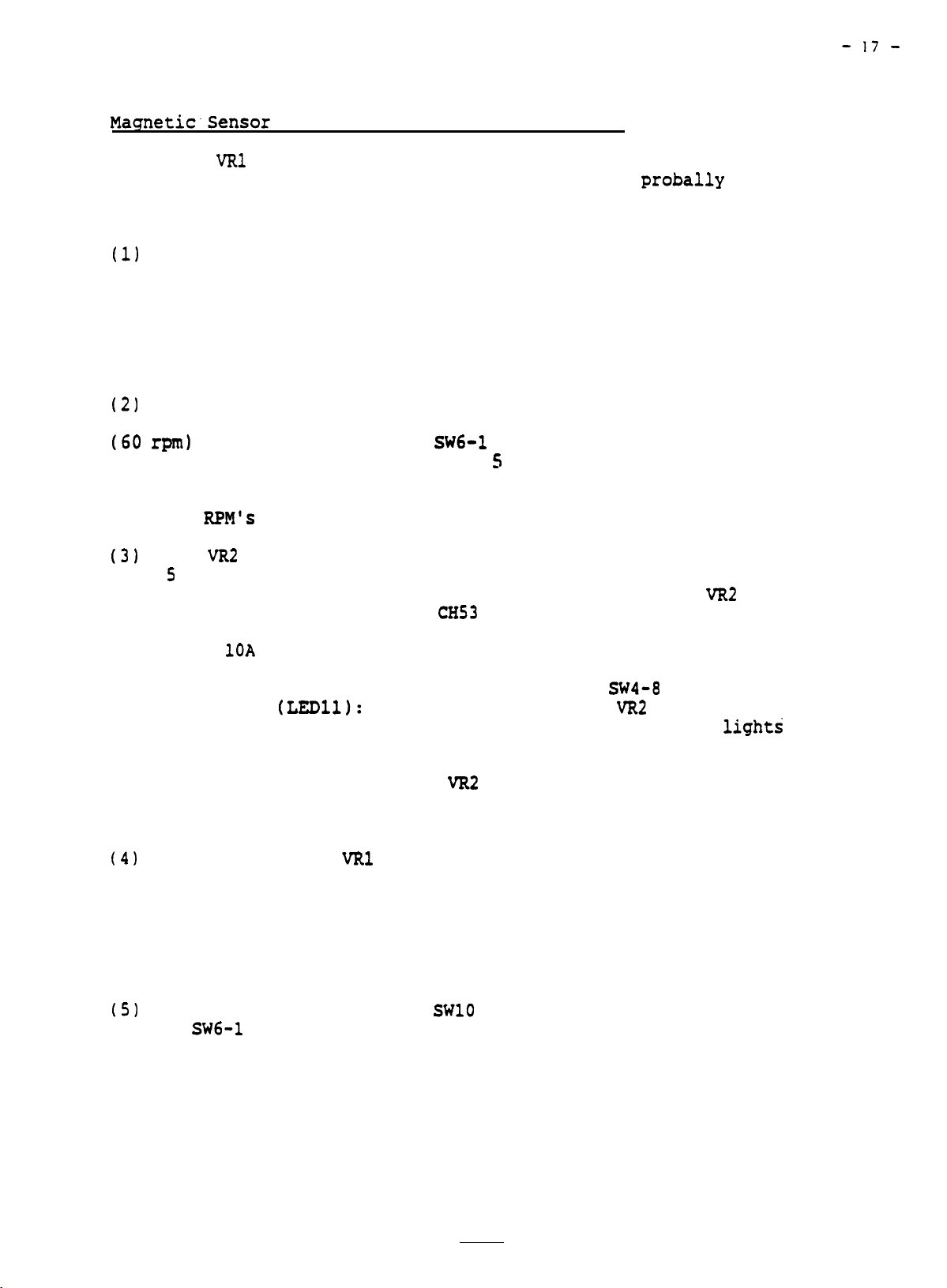
20 Vp-p is obtained between
Press ST2 and adjust
CH53
and DGA at orient. Note that
VR2
until1
the 20 Vp-p waveform occurs only momentarily at orient. Refer
to Figure
10A
for waveform. Repeat Method 1, as necessary,
increasing VR2 a half division each time until 20 Vp-p is
obtained.
Method 2
wise until LED11 lights then stop imediately. LED11
If
hunting occurs at orient, see
(LEDll):
Press ST2 and adjust
SW408
setting.
VR2
slowly clock-'
lighti
only at orient stop the first time and will usually stay on
until the next power up or spindle reset. Press ST2 again to
verify orientation.
insure adequate signal amplitude. Power
Increase
VR2
setting a half division to
‘OFF,
then ON or reset
spindle and press ST2 to verify orient.
(4)
Caution:
avoid any mechanical interference.
Adjust
VRl
(Position shift) as necessary to
This may involve measuring
the spindle position relative to axis movement as specified
by the machine manufacturer.
Example: At ATC, tool changer claw must align with spindle or
damage may occur when tools are changed.
(5)
After adjustment return
2. Set
SW6-1
to ON and press ST1 (Reset) to return the spind-
SW10
to original position in step
le controller to normal. Refer to Fig. 5 or Fig. 6 for location
of switches.
FR-SE Base Driver
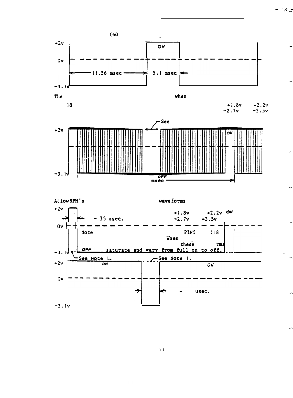
Waveforms
- 1.8:
Converter Base
+2v
ov
I_
The
converter waveform is visible only
L&D 18 should be ON.
Inverter
Base
+2v
ov
-3.1
Waveform:
I
__
,,,,,_,_J;_~___~~_
Waveform:
IJ.36
OFF
(2800
(60
Hz.)
Voltages
Hr.)
*
I
I
may vary,
rSee
mstc
_________,
I
uhen
the converter is
Positive range:
Negative range:
Note
1.
OFF
+1.8v
-2.7~
>
I
enabled.
to
+2.2v
to
-3.5~
The
above waveform
At low
RPM’s
ov
k+ ____
_____------I--t-----_____-_---
ov
-3.lv
Note :
the speed
30
Note
Waveforms
same time.
the voltages on one transistor
P side transistors and N side to N side transistors.
is
actually
at
Voltage
-
35 usec.
-
_____
1: Waveforms shown are with
kv Drive or
15 kv Drive or smaller)
on the P side can not be seen on the oscilloscope at the
They do not share a common. It may be helpful to compare
changing betvecn the
which the
range:
Positive:
Ncgacive: -2.7~
Larger).
OF?
-1
vaveforms
-_----_-b_t_---
When
60 -70
change slows and is
+1.8v
PINS
PINS is ON
the&
t+
to
another. Hint: Compare P side to
co
to
-3.5~
OFF
vavefo
usec.
bottom two waveforms.
visible.
+2.2v 0~
rl
(18
1
.
Figure
II
-
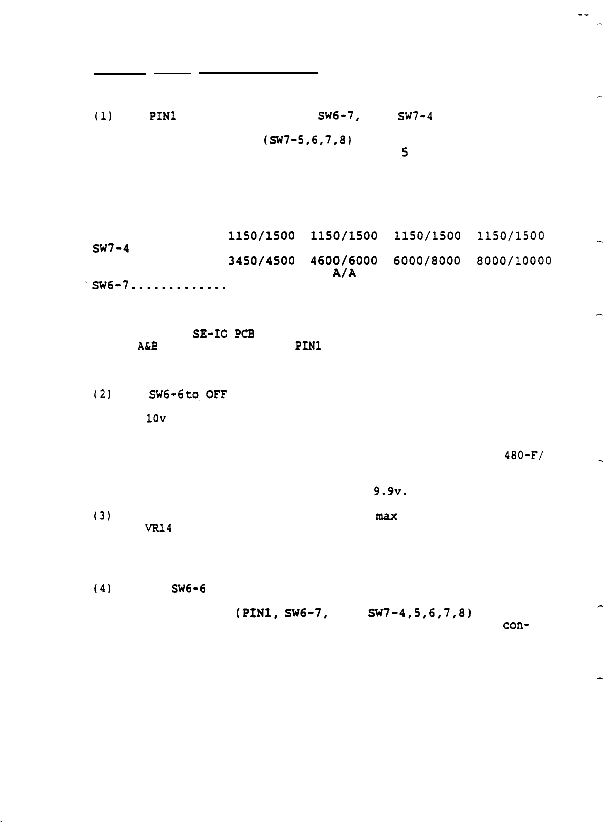
Procedure for Checking Base Driver Waveforms FR-SE
This procedure should be used if output transistors were
damaged and replaced or output transistors are suspected of
_
being damaged.
(1)
Before restorinq power to
the
machine switch
CBl
OFF.
This prevents power from being applied to the output tran-
sistors.
Disable breaker trip alarm by inserting jumper
(FB)
on Pin 4 of SE-IO Card. This is located on the lower right
corner of the card and to the right of the
inal.
Refer to lower right corner of Figure 7. A SPARE jumper
TB2
screw term-
strap can usually be found on the SE-CPU or SE-IO Cards.
(2)
Set dip switch
SW602
(Open loop)
OFF
and press ST1
(Reset) on the SE-IO Card. Refer to Figure 7.
(3)
Regeneration Transistor Check: (Converter)
Connect a
1.
ode (top) side of
shcrt
jumper wire between DGA and the cath-
D12
in middle of SE-IO Card. See
_._-
Figure 7.
Power CNC ON.
2.
lights with converter regeneration.
_
3.
Command the spindle
Confirm LED18 on SE-IO Card is ON. LED18
FWD
or REV (MO'3
or
M04).
Verify
that LED2 and LED3 or LED4 on the SE-CPU Card are ON.
4.
Check the waveforms at the following check points with
an ungrounded (isolated) oscilloscope. See Figure 11
for voltage and duty cycle specifications. Refer to
Figure 7 for locations of
CH
Point and resistor.
19
-
‘1 ’
_-
CH50
to right side R146
CH51
to right side R149
CH52 to right side R152
Note:
Leads of the resistors may have coating. Remove coating
CH53 to right side.
CH54
to o
CHSS
to ((
((
))
R155
I,
,*
if necessary before making measurements.
5. Power CNC
Remove the short jumper wire from DGA and D12.
*6.
(4)
Generation Transistor Check:
Power CNC ON.
5:
Command
Input a speed command of about
3.
Check the waveforms at the following check points with
4.
an ungrounded oscilloscope.
forms.
CH44 to right side R128
,y YCH45
. (5)
Power CNC OFF and return spindle controller to normal.
PIN4 OFF,
to left side R131
.YCH46
to left
SW6-2
OFF.
Verify LED2 is ON.
FWD
or REV.
Refer
to Figure 7 for
Verify LED3 or LED4 is ON.
side R134
ON, and press
(Inverter)
l/10
of top speed.
See to Figure 11 for wave-
location of CH Point.
CH47 to right
CH48 to
CH49 to
STl.
If check OK, turn
-
)(
"
side*
R137
,,
,*
,*
*,
CBl
ON.
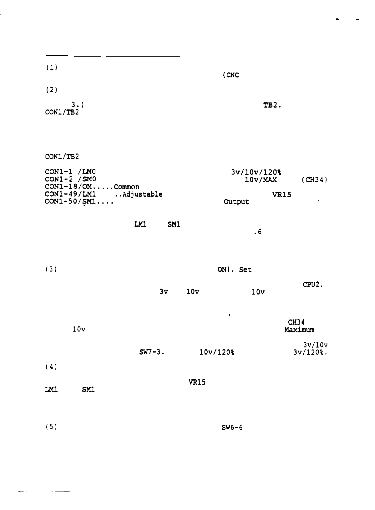
Maximum Speed Adjustment FR-SE
Note:
(1)
Overspeed alarm may be caused by missadjustment.
Set
PIN1
(on SE-IO card),
SW607,
and
SW704
on the SE-CPU
card according to the following information. For other
capacity/rpm settings
Sheet with the machine. Refer to Figure
Figure 7 for SE-IO
Note:
Motor base speed, top speed,
(SW705,6,7,8)
PCB
layout.
refer to Switch Setting
5
or
6 for SE-CPU and
and Kw capacity can be
found on the motor name plate.
Standard Motor:
Base Speed
sw7-4
TOP Speed
.............
PILL...........
.SW6-7.............
........
.........
1150/1500 1150/1500
3450/4SOO 4600/6000 6000/8000 8000/10000
ON
ON/OFF ON/OFF
B/B
New SE-IO PCB..... VR6
Old SE-IO PCB..... VR7
Note:
On old
A&B
is specified for
SE-X PCB
set
in place of VR6 were
A/A
OFF
VR6
VR6
VR7 to S (Middle of rotation) if
PIN1
above.
specified in the above table. VR7
11s0/1s00 1150/1500
ON/OFF
ON/OFF
A/A&B A&B/A&B
OFF
VR6
VR6
OFF
VR6
VR6
In step 2 adjust VR7
is no longer used on new SE-IO Cards.
(2)
SET
SW606
to,OFF
and press ST1 (Reset) on the SE-CPU PCB.
Adjust VR6 fully clockwise and then counterclockwise to
obtain
10~
at CH34 to
DGA.
Refer to Figure 7 for location of
adjustment and check point.
Alternate Method: This method has low accuracy and should
only be used for rough adjustment. For EPROM versions
490-C and later.
Adjust VR6 fully clockwise and then turn it
480-F/
slowly counter-clockwise until LED17 lights. LED17 lights
when voltage at CH3 to DGA is 9.8 to
(3)
The speed meter should be reading
Adjust
If fixed output is used
VR14
to set Maximum speed reading on the speed meter.
or
encoder, VR14 will have no effect
9.9v.
max
RPM at this time.
on the meter reading or display. Refer to Meter Output
Adjustment Procedure
(4)
Return
SW606
to the ON position and press ST1 (Reset) on
the spindle drive to
switches and
pins
according to the Switch Setting Sheet for the spindle
for
more information.
return
(PfNl, SW607,
it to normal operation. Confirm
and
SW7=4,S,6,7,8)
are set
con-
troler on that machine. If not correct, record setting
difference and repeat adjustment procedure.
-
21
Meter Output Adjustment FR-SE
(1)
These adjustements,
operating conditions for the spindle.
(21
Some machines use the fixed voltage outputs for which
if used, should be made under normal
(CNC
ready)
there is normally no adjustment on the spindle drive. (See
step
CONl/THZ
3.)
Outputs are
available
from
connection table below.
CON1 and/or
TB2.
Refer to
-
Note:
Some
machines used the encoder feedback for spindle rpm
display and the spindle speed meter output is not used
by the CNC.
CONl/TH2
CONl-1 /LMO
CONl-2 /SMO
CONl-18/0M...
CONl-49/LMl . .
CONl-SO/SMl....
Note:
Connections:
. . ..Fixed Load Meter Output
. . ..Fixed
..Common
..Adjustable
Adjustable Speed Meter
LMO and
by 220 ohms.
SMO
are voltage outputs, with current limited
LM1
Speed Meter
(Ground)
Load Meter Output
and
SMl
are 1 ma. current outputs,
Output
Cutput
3v/lOv/120%
lOv/MAx
(See
RPM
vR15
vR14
note)
(CH34)
*
with adjustment range of approximately .6 to 1.5 ma.
Note:
Some adjustement
may
still be necessary on the machine
or CNC side even when fixed voltage outputs are used.
(3)
CNC ON and READY (LED2 on SE-CPU
(Meter calibration)
OFF
and press
ST1 (Reset) on SE-CPU card.
Refer to left center of Fig. 5 for CPU1 and Fig. 6 for
OPTIONAL: Verify LMO is 3v or
nected.
If fixed outputs are incorrect refer to the following
1Ov
and SMO
ON).,Set
Dip Switch 6-6
is
10~
CPUZ.
when discon-
note and Maximum Speed Adjustment Procedure.
.
Note:
If the speed meter output is incorrect, check
1Ov
to DGA. If CH34 is high or low, refer to
Speed Adjustment Procedure.
er speed alarm.
by dip switch
Load meter output can be set for
SW773.
ON is
Misadjustment can cause ov-
lOv/120%
and OFF is
CR34
for
Maxj.mum
3v/lOv
3v/120%.
(4)
The Load meter should read 120% and Speed
should read Maximum
external panel meter/s.
LMl
and
bottom right
Note:
(5)
After adjustment is complete,
SMl
are used
of
Fig.
Outputs may come from CON1 instead of TB2.
(Reset) on SE-CPU or power CNC
RPM.
This is usually full
Adjust
for the correct
VR15
and VR14 respectively if
meter
reading. Refer to
7 for adjustment.location.
set
OFF/ON
SW6-6
ON and press ST1
to reset if
meter,
scale on the
if used,
CNC
pro-
vides a reset signal to the Spindle Drive. (Normal)
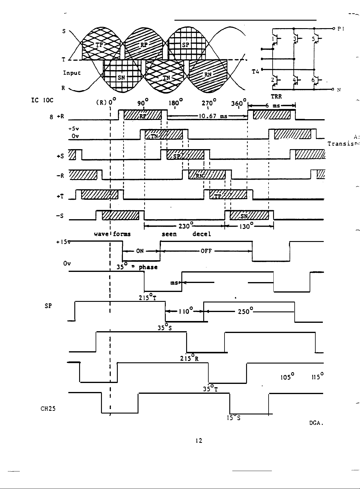
FR-SE Converter Output Firing Sequence
R4
-
s4
60 HZ
IC 1oc
SE-IO
Pin 8
Pin 2 -T
Pin 10
Pin 4
Pin 12
Pin 6
The following
RP
CH23
TN
CH28
SP
CH26
RN
CH27
TP
CH24
Phase
+R
+S
-R
+T
-S
+I50
ov
-
CR) $I0
wavelforms
I
i
I
I
I
I
I
can
I
-OFF-
35’
R phase
I
I
I
I
I
I
I ’
be
4
-5.1
I
21S0T
phase
seen
I
-IloO-
35's
2?0°
at
decel
or
with the converter enabled.
msr
i II.56 ms
f
phase
21S0R
phase
TO
36,0°
1
.
2so”
Max. ON
at 60 Hz.
Range: 4.9 Co 5.3 ms‘
TRS
I
time 5.35 ms
IOSO
co
-
TRT
I ISO
Diode
Conduct
Shaded
Transisr;
Firing
TRR-I
TRT-6
TRS-3 _
TRR-2
TRT-5
ic
A:
SN
CH25
I
I
I
I
I
The above check points
l
35'T
phase
2
IS'S
can
be seen ac the same time using AGA or
Figure
I2
phase
.
DGA.
TRS-4
-
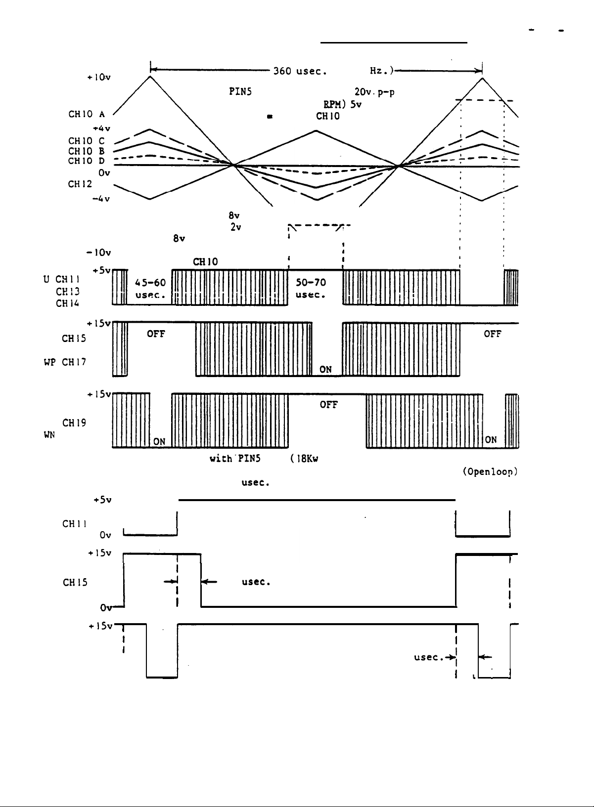
FR-SE Inverter Waveforms
-
23
-
CH12: 2800
U CHII
V
CH13
W
CHlk
UP
CH15
VP CH16
UP CHl7
C: PIN5
D: PIN5
-IOv
+5v
Ov
+15v
ov
-360
A:
B: PIN5 OFF
PIN5 OFF
ON (Zero RPM)
ON (Max. RPM) 2v p-p
Hr.
In
8v
p-p
open loop
CHlO
is max.
usec.
PINS
OFF (Zero RPM)
(Max.
2.5 x
-
8v
p-p
,-----!-
I
I
V
I
f
(2800
RPM)
CHIO
PIN5 ON
I
I
I
I
Hr.)'
2Ov.p-p
5v
p-p
+15v
UN CH18
VN
CHl9
UN
CH20
ov
The
waveforms shown
these waveforms may
Example
waveforms showing 26
with'PIN5
saturate and vary from full on to full off.
OFF
usec.
(18Kw
drive or larger). When PIN5 is on
interlock for output transistors.
are
+5v
7
CHII
CHl5
+l5v
CH18
Note: Times and voltages may vary with differrent drives.
ov
ov
I
,
I
I
I
i
I
I
J
+
26
usec.
26
usec.-$
(Open
loop)
1
I
.
I
I
c
I c . .
r
I
i
I
I
I
c
Figure 13
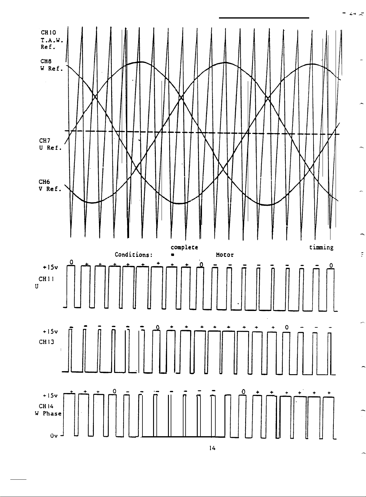
FR-SE Inverter Waveforms
-
L+<
Does not show current feedback or
may be differrent.
+lSv
CHll
U
Phase
ov
_ - -
+15v
CHl3
V Phase
ov
Conditions:
- _ _
I
TAW - 2800 Hz.,
.
.
complete
I
._ _ - -
c
error signals. Voltages and
Motor
frequency approx. 1.55 Hz, 4670
P ”
-
-
-
0 + +
4
timming
!
I
Figure
-
w
14
.
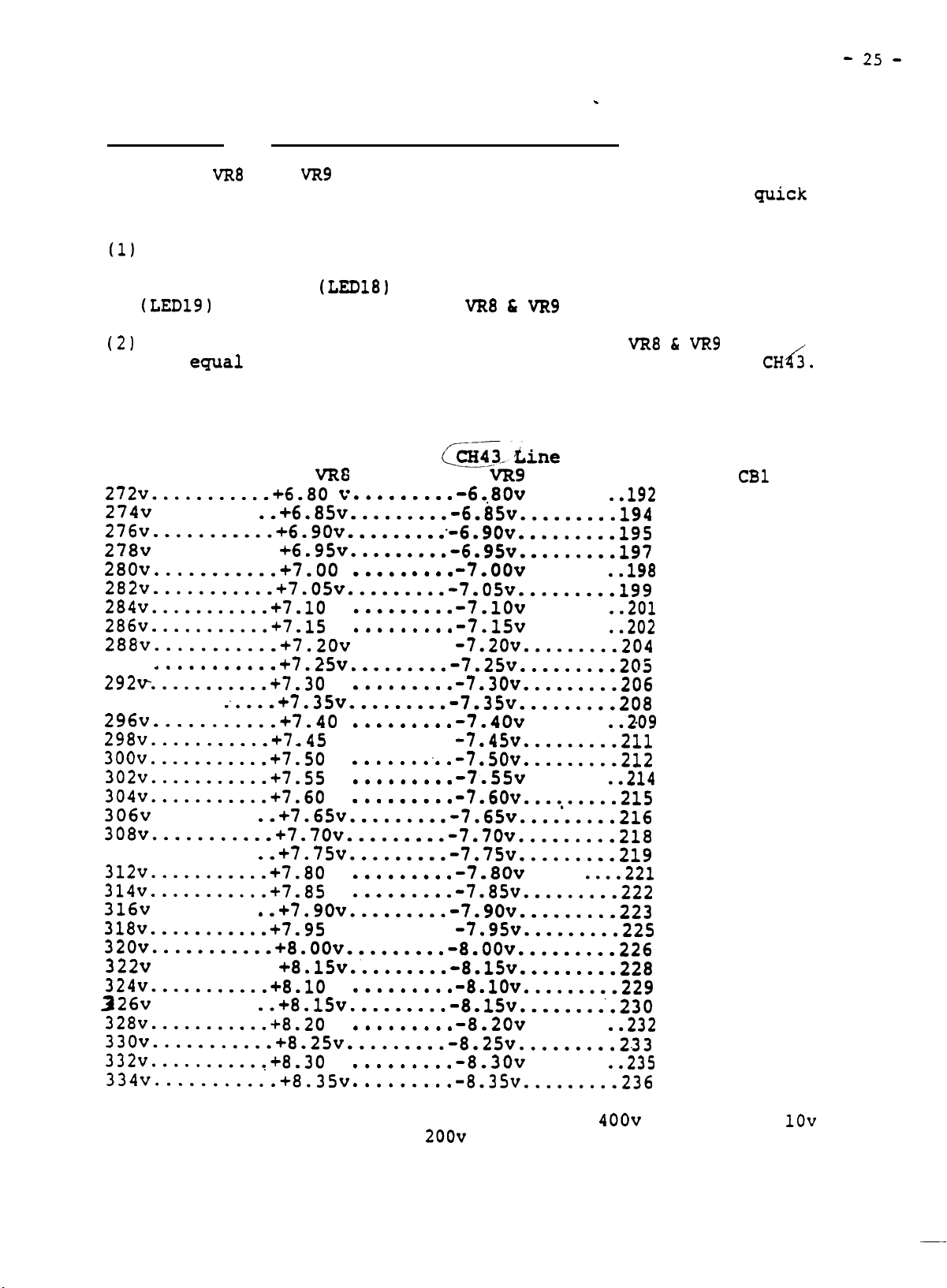
Adjustment of Converter Enable Circuit FR-SE
- 25 -
Note:
turn off (LED 18 ON) or the converter will not turn on
enough and cause damage to output transistors
(1)
and LED20 are ON and LED18 is OFF. The condition
enabled indicator
or
(2)
obtain
Repeat adjustment until equal.
of check points and adjustments.
If
VR8
and
VR9
are misadjusted the converter will not
quick
or
capacitors.
The drive should be in ready condition only. Verify LED19
of
converter
(LED181
(LED191
may be incorrect if
The basic adjustment involves adjusting
equal
positive
and base transistor cutoff indicat-
VR8 & VR9
and
negative voltages at CH42 and
Refer
are misadjusted.
VR8 & VR9
to
CH&.
to Figure 7 for location
Use the following table as a
guide for approximate voltages that should be obtained.
P-N DC
Voltage
272~...........+6.80 v
274~
.........
276v...........+6.9Ov........~-6.9Ov.........l95
278~ ...........
280~...........+7.00
282v...........+7.05v.........~7.05v.........199
284~...........+7.10
286~...........+7.15
288~...........+7.20~
290v
...........
292v...........+7.30
294v
......
:....+7.35~.........-7.35~.........208
296v...........+7.40
298v...........+7.45
3oov...*.......+7.50
302~...........+7.55
304~...........+7.60
306~
.........
308v...........+7.70v.........~7.70v.........218
310v
.........
312~...........+7.80
314~...........+7.85
316~
.........
318v...........+7.95
32Ov...........+8.OOv.........~8.OOv.........226
322~
...........
324~...........+8.10
326~
.........
328~...........+8.20
33Ov...........+8.25v.........-8.25v.........2.33
332~...........+8.30
334~...........+8.35~
CH42 P-N
vR8
.........
cCz.-Line
VR9
-6.8Ov
.......
..+6.8%.........-6&v.........l94
Approx. VAC
Input at
..192
v
v
v
+6.9%.........-6.9%.........197
v
.....
....
-7.OOv
.......
v
..198
v
v
v
.........
v
.........
......... -7.20~.........204
+7.25~.........-7.25~.........205
v
.........
-7.lOv
-7.15v
.......
.......
..201
v
..202
v
v
v
-7.30~.........206
v
v
v
..
.......
v
.........
v
..........
v
.........
v
.........
..+7.65~.........-7.65~...,'.....216
-7.4ov
.......
-7.45~.........211
-7.50~.........212
-7.55v
.......
-7.60~.........215
..2.09
v
v
v
..214
v
v
v
v
..+7.75v.........-7.75v.........219
v
v
.........
.........
-7.80~
.....
..*.221
-7.85~.........222
..+7.9ov.........-7.9ov........*223
v
.........
-7.95v.........225
v
v
v
v
v
v
+8.15~.........-8.15~.........228
v
.........
-8.lOv.........229
..+8.15~.........-8.15~........'.230
v
.........
-8.20~
.......
v
v
v
..232
v
v
v
.........
.........
-8.30~
.......
-8.35~.........236
..235
v
v
CBl
Note:
This table is based on DC
at CH42 and an AC input
of
200~
output of
producing
-7.07-v at CH43.
400~
generating
10~
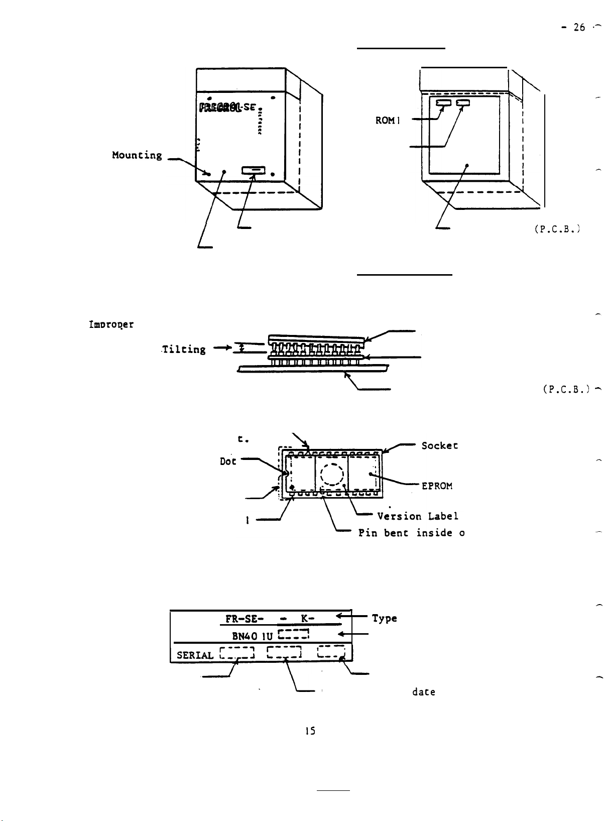
EPROM Location
ROM1
Houncing
Screws
ImDtoDer
Insertion:
(Not fully
Bent Pins:
L
Nameplate
L
Front Panel
Tilting
inserted)
Pin bent outside
of she
socke
ROM2
L,
SE-CPU Card
(P.C.B.)
EPROM Insertion
EPROM
Socket
Printed Circuit Board
(P.C.B.) -
_
Notch or
P
.C.B. Outline
Do.c
Pin
Details of the Nameplate:
TYPE
FR-SE-
BN40
Serial number
-
K-
1IJ t::z
Figure
4
’
Type
4
Parts List BN number
Check number
Manufacturing
IS
date
f the socket.
-
- 27 -
Instructions for Changing FR-SE EPROM
(1) Please make sure that all power sources are turned off
before changing EPROM. Because
CBl
in the spindle drive does
not remove power from the circuit boards it is necessary to
turn off the machine main breaker.
(2).
Note the position of the name plate and the locations
the EPROM's in Figure 15.
hind the front panel.
The SE-CPU card is located just be-
Two EPROM's
(ROM1 & ROM21
are located
of
on the upper left side of the CPU card.
(3)
Remove the EPROM very carefully with a ROM puller. Be
sure not to bend the pins on the EPROM. The EPROM can be
removed by prying very carefully on the corners between the
EPROM and the socket with a small flat
screw.driver.
Do not
pry against or damage the printed circuit board.
!4)
Confirm the version on the
EPROK
label and note number
for proper socket location. Example: Al in ROM1 socket.
(5)
Locate notch or dot on EPROM and align that end of the
EPROM with the notch on the printed circuit board outline.
Refer to Figure 15 for detail.
Carefully start all pins of
the EPROM in the socket. Then apply firm pressure to seat the
EPROM in the socket.
Support the printed circuit board so
that excessive bending does not occur. In the case of a new
EPROM it may be necessary to bend all of the pins at right
angles to the EPROM case before attempting insertion.
(6)
Make sure all of the pins on the EPROM are properly in-
serted in the socket.
pins bent under the EPROM or bent out.
Inspect for tilting of the EPROM and
Refer to Figure 15 for
detail.
(7)
Please record the machine serial number, the new EPROM
version from the label,
drive nameplate.
Please return this information and the old
and the information form the spindle
EPROM's to Mitsubishi.
(8)
Refer to Figure 15 for location and details of the nameplate.
Machine Serial Number
Spindle Drive Type...
BN Number............
SE Serial Number.....
Manufacturing Date...
Check Number.........
EPROM Version........
.
.
. .
.
.
.
.
.
.
.
.
.
.
.
.
Note:
machine.
Always keep the original hinge cover panel with the
This keeps the above information correct for that
machine which is necessary for proper servicing of the drive.
 Loading...