

Page 1
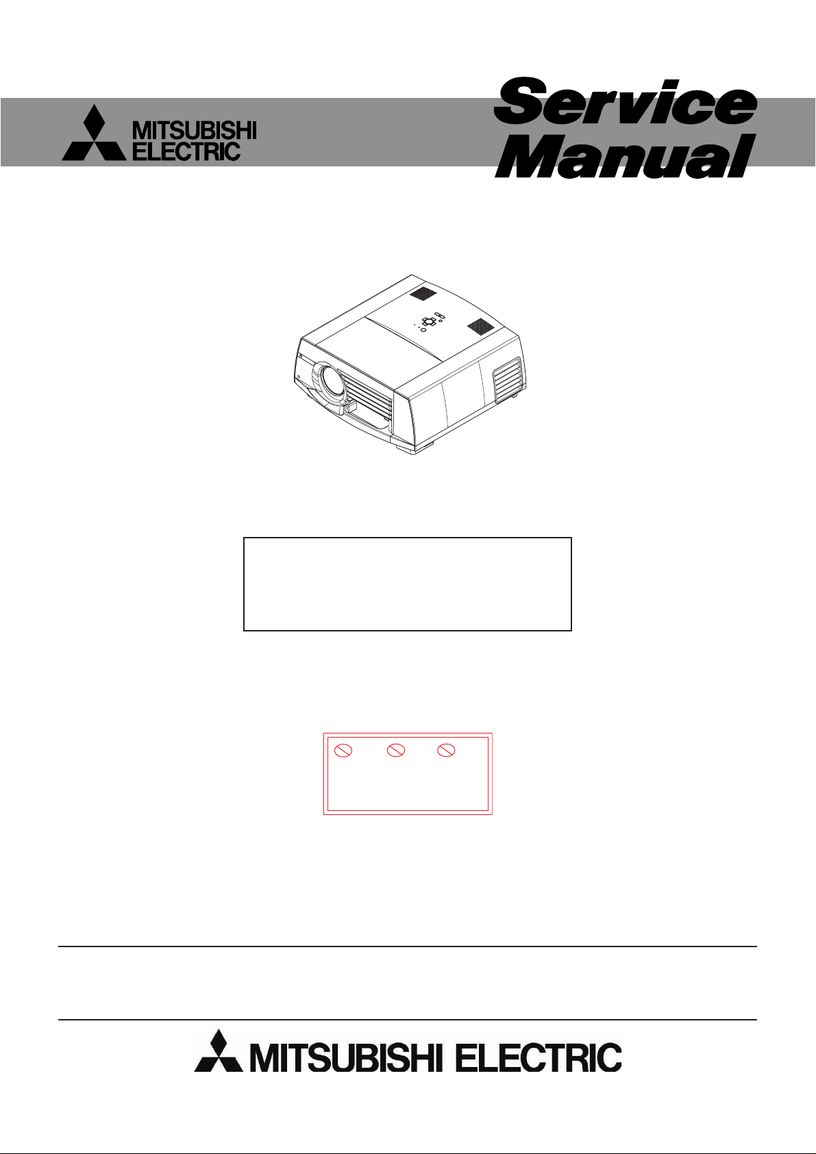
LCD PROJECTOR
LC61 CHASSIS
MODEL
2008
FL7000U
This model is RoHS-compliant.
Provide servicing referring to “NOTES
FOR SERVICING RoHS-COMPLIANT
PRODUCTS” described in the service
manual.
Pb Solder, Pb Joints, Pb PCA
This product uses lead-free solder
on the circuit boards. For repairing
circuit boards, see "Precautions for
resoldering" in this Service Manual.
CAUTION
Before servicing this chassis, it is important that the service person reads the “SAFETY PRECAUTIONS” and “PRODUCT
SAFETY NOTICE” in this service manual.
Copyright © 2008 Mitsubishi Electric Corporation All Rights Reserved.
Page 2
NOTES FOR SERVICING RoHS-COMPLIANT PRODUCTS
Follow the notes and instructions below when servicing RoHS-compliant
products.
1. For RoHS-compliant products, be sure to use RoHS-compliant service parts.
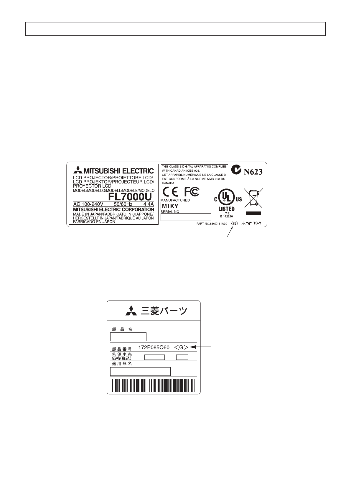
2. Check the presence of <G> marking on the rating plate to distinguish RoHScompliant product from non-RoHS-compliant product.
<G> marking
With <G> marking: RoHS-compliant product
Without <G> marking: Non-RoHS-compliant product
<Sample>
Mark position
3. Labels of RoHS-compliant service parts bear <G> marking for identifi cation purpose.
<Sample>
Parts Name
Parts No.
Model Name
E05R
Mark position
4. Don’t use non-RoHS-compliant parts with RoHS-compliant products.
5. Service parts for RoHS-compliant products are listed in the parts catalog contained
in the service manual.
- 2 -
Page 3

SPECIFICATIONS
• Rated Voltage
•
Power Consumption
•
Display Technology
• Projection Lens
•
Light Source Lamp
• Image Size
(projection distance)
•
Maximum Resolution
• S-Video Input
• Video Input
• Component Video Input
: AC 100 to 240V ; 50/60Hz,
• Analog Input
: 4.4A
:
1.1 inch LCD panel ; 3 pieces (for R,G,B)
:
Pixels ; 1,920 × 1,080 = 2,073,600 pixels
Total 6,220,800 pixels
:
Active pixel rate ; 99.9 % or more (each panel)
•
: F 1.8 - 2.1 f = 51 - 64 mm
: 275 W
:60 to 250 inch
(projection distance ; 2.6 to 11.2 m)
:
Computer signal
Maximum resolution ; 1,920 × 1,080 dots
(Compressed in the case of 1,600 × 1,200 dots)
Digital Input (DVI)
• Audio Input
• Speaker
• Control Terminal/
Others
• Dimensions
(not including protrusion)
Panel resolution ; 1,920 × 1,080 dots
:Video signal
NTSC/PAL/SECAM/4.43NTSC/PAL-M/PAL-N/PAL-60
• Weight
:Component signal
480i,480p,576i,576p,720p,1080i,1080p
•
Panel resolution ; 1,920 × 1,080 dots
:
Luminance signal ; 1.0 V(p-p) 75Ω (negative sync)
Chrominance signals ; 0.286 V(p-p) 75Ω (burst signal)
Operating temperatures
: 1.0 V(p-p) 75 Ω (negative sync)
: YC
BCR
;
Y ; 1.0 V(p-p) 75 Ω (negative sync)
C
0.7 V(p-p) 75 Ω
BCR ;
: RGB ;
0.7 V(p-p) 75 Ω (negative sync)
: YCBCR ;
Y ; 1.0 V(p-p) (negative sync)
C
: HD/CS ;
: VD ;
:
: 350 mVrms, 10 k
0.7 V(p-p)
BCR ;
TTL level (negative or positive polarity)
TTL level (negative or positive polarity)
DVI-D interface (TMDS single link) with HDCP
Ω or more
: 10 W mono Round type ø 4.5 cm × 1
: RS-232C (D-SUB 9 pin),USB,
LAN (RJ-45),REMOTE IN/OUT
: 371 (W) × 207 (H) × 434 (D) mm
(projector only)
443 (W) × 207 (H) × 434 (D) mm
(including the terminal cover)
: 9.8 kg (projector only)
: 10.5 kg (including the terminal cover)
: + 41 °F (+ 5°C) to 104 °F (+ 40 °C)
• Weight and dimensions shown are approximate.
• Design and specifi cations are subject to change without notice.
- 3 -
Page 4

CONTENTS
– FILE “COVERPGE” –
NOTES FOR SERVICING RoHS-COMPLIANT PRODUCTS ............................................................................... 2
SPECIFICATIONS ................................................................................................................................................. 3
CONTENTS ........................................................................................................................................................... 4
– FILE “EXPOSED” –
TRADE MARK, REGISTERED TRADEMARK ...................................................................................................... 1
PRODUCT SAFETY NOTICE ............................................................................................................................... 1
SAFETY PRECAUTIONS ...................................................................................................................................... 2
PRECAUTIONS FOR RESOLDERING ................................................................................................................. 3
PCB LOCATION .................................................................................................................................................... 4
EXPOSED VIEW ................................................................................................................................................... 6
L VP ASSY ........................................................................................................................................................ 6
Chassis 1 ASSY ............................................................................................................................................... 8
Chassis 2 ASSY ............................................................................................................................................... 10
Bottom case unit .............................................................................................................................................. 12
T erminal ASSY ................................................................................................................................................. 13
Optical unit 1 .................................................................................................................................................... 14
Optical unit 2 .................................................................................................................................................... 16
POSITION ADJUSTMENT OF MULTI LENS A ..................................................................................................... 17
DISASSEMBL Y ................................................................................................................... .................................. 18
1.Removal of the terminal cover ASSY ............................................................................................................ 18
2.Removal of the BOO PCB ASSY and BOO SUB PCB ASSY ....................................................................... 18
3.Removal of the lens unit and zoom focus motor ........................................................................................... 19
4.Removal of the top case unit and KEY PCB ASSY ...................................................................................... 20
5.Removal of the IRF PCB ASSY .................................................................................................................... 21
6.Removal of the MOTOR PCB ASSY ............................................................................................................. 21
7.Removal of the IRR PCB ASSY .................................................................................................................... 21
8.Removal of the speaker ................................................................................................................................ 22
9.Removal of the power fan ............................................................................................................................. 22
10.Removal of the MAIN PCB ASSY ............................................................................................................... 23
11.Removal of the TERMINAL PCB ASSY ...................................................................................................... 23
12.Removal of the DRIVE PCB ASSY and LCD block .................................................................................... 24
13.Removal of the drive fan ............................................................................................................................. 25
14.Removal of the PBS fan ............................................................................................................................. 25
15.Removal of the optical unit ......................................................................................................................... 26
16.Removal of the POWER PCB ASSY .......................................................................................................... 27
17.Removal of the lamp power unit ................................................................................................................. 28
18.Removal of the FILTER PCB ASSY and INLET PCB ASSY ....................................................................... 28
19.Removal of the POWER SUB PCB ASSY .................................................................................................. 29
20.Removal of the lamp fan ............................................................................................................................. 30
21.Removal of the LCD fan ............................................................................................................................. 30
22.Removal of the exhaust fan ........................................................................................................................ 31
23.Removal of the lens shift motor .................................................................................................................. 31
24.Removal of the lamp box ............................................................................................................................ 32
LAMP REPLACEMENT ......................................................................................................................................... 32
LEAD DRESS ........................................................................................................................................................ 33
PACKING ............................................................................................................................................................... 38
– FILE “MAINTENA” –
LAMP REPLACEMENT ......................................................................................................................................... 1
MAINTENANCE .................................................................................................................................................... 3
HOW TO USE THE LAMP JIG .............................................................................................................................. 4
DUST ON LCD PANEL .......................................................................................................................................... 5
RESET OF THE THERMAL PROTECTOR ........................................................................................................... 5
SERVICE COMMANDS ........................................................................................................................................ 6
Display the operation status screen ................................................................................................................. 6
Reset to the factory settings ............................................................................................................................ 6
Reset the lamp operating time ......................................................................................................................... 6
LIFE TIME OF THE CONSUMABLE PARTS ........................................................................................................ 7
FUNCTION MENU(SETTING MENU ONLY FOR SERVICE) ............................................................................... 8
REPLACEMENT OF THE MAIN PCB ASSY ......................................................................................................... 9
REPLACEMENT OF THE TERMINAL PCB ASSY ................................................................................................ 10
GAMMA ADJUSTMENT(WHITE BALANCE ADJUSTMENT) ............................................................................... 10
UNIFORMITY DATA TRANSFER .......................................................................................................................... 12
COLOR UNIFORMITY ADJUSTMENT ................................................................................................................. 13
DOWNLOAD OF THE FIRMWARE ....................................................................................................................... 15
CRITERIA OF THE DEFECT PIXEL ON THE LCD PANEL(FOR REFERENCE PURPOSE) .............................. 16
ABOUT LASER BEAM .......................................................................................................................................... 18
- 4 -
Page 5

– FILE “ELCTADJ” –
ELECTRICAL ADJUSTMENTS ............................................................................................................................. 1
Necessary Equipment and Connecting ........................................................................................................... 1
Test Signal ....................................................................................................................................................... 1
Adjustment with Microsoft
®
Windows® 95/98/Me/XP Operating System ......................................................... 2
Adjustment Procedures ................................................................................................................................... 3
– FILE “DIAGNO” –
DIAGNOSIS INFORMATION ................................................................................................................................. 1
DIAGNOSTIC SOFTWARE,TO READ WARNING HISTORY(PCGC8 Ver.2) ....................................................... 3
SPECIFICATION OF RGB SIGNALS IN EACH COMPUTER MODE OF THE PROJECTOR .............................. 5
– FILE “DIAGFLOW” –
DIAGNOSIS FLOW CHART .................................................................................................................................. 1
Image system .................................................................................................................................................. 1
Power source system 1 ................................................................................................................................... 2
Power source system 2 ................................................................................................................................... 3
Power source system 3 ................................................................................................................................... 4
– FILE “PCCONTRL” –
Controling the prijector using a personal computer ............................................................................................... 1
– FILE “PARTSLST” –
PARTS LIST .......................................................................................................................................................... 1
PCB LOCATION .............................................................................................................................................. 2
EXPOSED VIEW ............................................................................................................................................. 3
LVP ASSY .................................................................................................................................................. 3
Chassis 1 ASSY ......................................................................................................................................... 4
Chassis 2 ASSY ......................................................................................................................................... 5
Bottom case unit ........................................................................................................................................ 6
Terminal ASSY ........................................................................................................................................... 6
Optical unit 1 .............................................................................................................................................. 7
Optical unit 2 .............................................................................................................................................. 8
PACKING ......................................................................................................................................................... 9
ELECTRICAL PARTS AND OTHERS .............................................................................................................. 10
– FILE “SCHEMATC” –
IC BLOCK DIAGRAMS
SCHEMATIC DIAGRAMS
PRINTED CIRCUIT BOARD PARTS LAYOUT
- 5 -
Page 6

TRADEMARK, REGISTERED TRADEMARK
Microsoft Windows 95/98/Me/XP are either registered trademarks or trademarks of Microsoft Corporation in the United States
and/or other countries.
Other brand or product names are trademarks or registered trademarks of their respective holders.
PRODUCT SAFETY NOTICE
Many electrical and mechanical parts in the projector have special safety related characteristics. These characteristics are often
not evident from visual inspection nor can the protection afforded by them necessarily be obtained by using replacement components rated for higher voltage, etc. Replacement parts which have these special safety characteristics are identifi ed in this ser-
vice manual. Electrical components having such features are identifi ed by shading on the schematic diagram and the parts list
of this service manual and by the supplementary sheet for this chassis to be issued subsequently.
- 1 -
Page 7
A
SAFETY PRECAUTIONS
North america
NOTICE: Observe all cautions and safety related notes located inside the cabinet and on the chassis.
Warning
1. Operation of this projector outside the cabinet or with the cover removed presents a shock hazard from the projector power
supplies.
2. When a short-circuit has occurred, replace those components that indicate evidence of overheating.
3. Grounding circuit continuity is vital for safe operation of equipment. Do not remove ground connection while the power cord
is still connected to the supply. Disconnect supply before servicing.
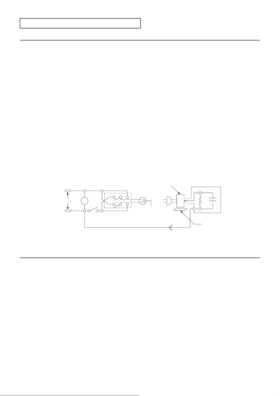
Leakage current check
Before returning the projector to the customer, it is recommended that leakage current be measured according to the follow-
ing methods.
1. Cold check
With the AC plug removed from the AC 100 to 240 V, place a jumper across the two AC plug prongs. Turn the projector AC
switch on. Using an ohm-meter, connect one lead to the AC plug and touch the other lead to each exposed metal part (metal
cabinet, screwheads, metal overlays, etc.), particularly any exposed metal part having a return path to the chassis. Exposed
metal parts having a return path to the chassis should have a minimum resistance reading of 1 megohm. Any resistance be-
low this value indicates an abnormality which requires corrective action. Exposed metal parts not having a return path to the
chassis will indicate an open circuit.
2. Hot check
Use the circuit in fi gure to perform this test.
(1) With switch S1 open, connect the projector to the measuring circuit. Immediately after connection, measure the leakage
current using both positions of switch S2, and with the switching devices in the projector in all of their operating positions.
(2) Switch S1 is then closed, energizing the projector. Immediately after closing the switch, measure the leakage current us-
ing both positions of switch S2, and with the switching devices in the projector in all of their operating positions. Current
measurements of items (1) and (2) are to be repeated after the projector has reached thermal stabilization. The leakage
current must not be more than 0.5 milliampere.
Projector
AC milliammeter
S2
C 100 to 240 V
V
S1
Grounding supply conductor
GH
(grounding)
open
B
Figure
A
Insulating table
Europe, other than USA
NOTICE: Observe all cautions and safety related notes located inside the cabinet and on the chassis.
Warning
1. An isolation transformer should be used between the projector and the AC supply point before any test/service is performed
on a LIVE chassis projector.
2. Operation of this projector outside the cabinet or with the cover removed, involves a shock hazard from the projector power
supplies. Work on the projector should not be attempted by anyone who is not thoroughly familiar with precautions neces-
sary when working on high voltage equipment.
3. When service is required, observe the original lead dressing. Extra precaution should be given to assure correct lead dress-
ing in the high voltage area. Where a short-circuit has occurred, replace those components that indicate evidence of over-
heating.
Leakage current cold check
Before returning the projector to the customer, it is recommended that leakage current be measured according to the following
methods.
With the AC plug removed from the AC source, place a jumper across the two AC plug prongs. Turn the projector AC switch on.
Using an 500 V D.C. Insulation Tester, connect one lead to the jumpered AC plug and touch the other lead to each exposed metal part (screwheads, etc.), particularly any exposed metal part having a return path to the chassis. Exposed metal parts having a
return path to the chassis should have a minimum resistance reading of 4 megohm. Any resistance below this value indicates an
abnormality which requires corrective action.
- 2 -
Page 8
PRECAUTIONS FOR RESOLDERING
Lead-free solder is handled in a different way from eutectic solder. See below for details.
How to distinguish circuit boards using lead-free solder from those using
eutectic solder
Circuit boards using lead-free solder
A mark of Solder, Joints, PCA or LFS (for limited marking space) is printed near the board assembly number on
the component side.
Circuit boards using eutectic solder
Circuit boards using eutectic solder are divided into two groups.
- Boards having no mark of
number.
- Boards having a mark of
pen near the board assembly number.
* Only when there is a limited marking space on the board,
PCA as P.
* Circuit boards using lead-free solder and those using eutectic solder may be used together in the same product.
Instructions for resoldering
- For circuit boards using lead-free solder, use lead-free solder.
- For circuit boards using eutectic solder, use eutectic solder.
- Separate the soldering iron for lead-free solder from that for eutectic solder completely for use.
(It is prohibited to use a same soldering iron for lead-free solder and eutectic solder.)
- For lead-free solder, it is advisable to use a soldering iron of at least 40 W because lead-free solder has a melting point approx. 35°C higher than that of eutectic solder as conventionally used. For wire solder, use M705ESC made by Senju Metal
Industry Co., Ltd.
- To remove solder, you can use desoldering wires for eutectic solder as conventionally used.
Solder, Joints, PCA or LFS (for limited marking space) near the board assembly
Solder, Joints, PCA or LFS (for limited marking space) that is painted out by a felt-
Solder may be indicated as S, Joints as J, and
- 3 -
Page 9
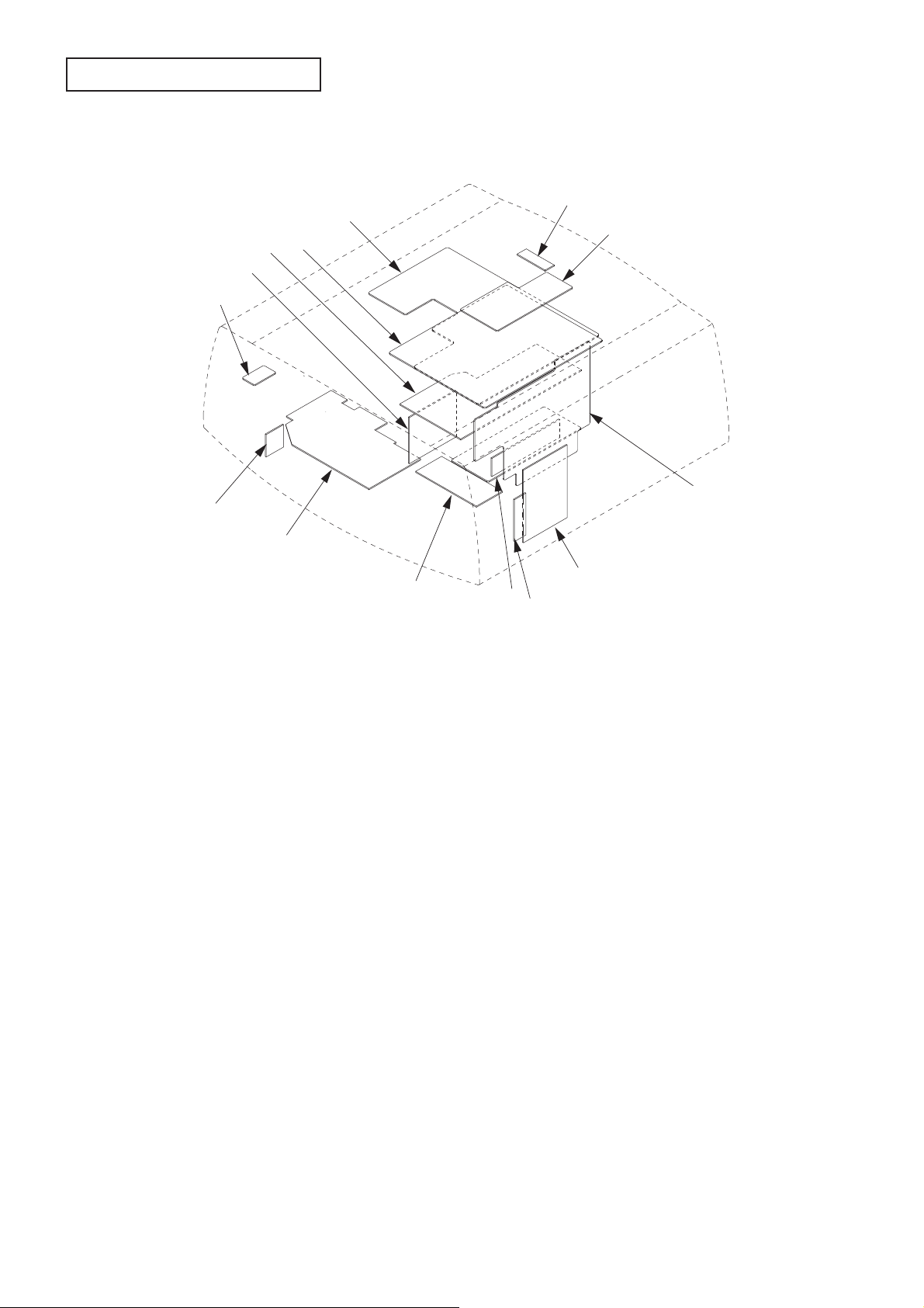
PCB LOCATION
14
5
4
3
2
1
13
12
11
6
7
8
9
10
Fig.1
- 4 -
Page 10

Parts list : See page 2 of PARTS LIST
Item No. Part name
1 IRF PCB ASSY
2 FILTER PCB ASSY
3 POWER PCB ASSY
4 MAIN PCB ASSY
5 DRIVE PCB ASSY
6 IRR PCB ASSY
7 KEY PCB ASSY
8 TERMINAL PCB ASSY
9 BOO PCB ASSY
10 BOO SUB PCB ASSY
11 Lamp power unit
12 INLET PCB ASSY
13 POWER SUB PCB ASSY
14 MOTOR PCB ASSY
Table 1
- 5 -
Page 11
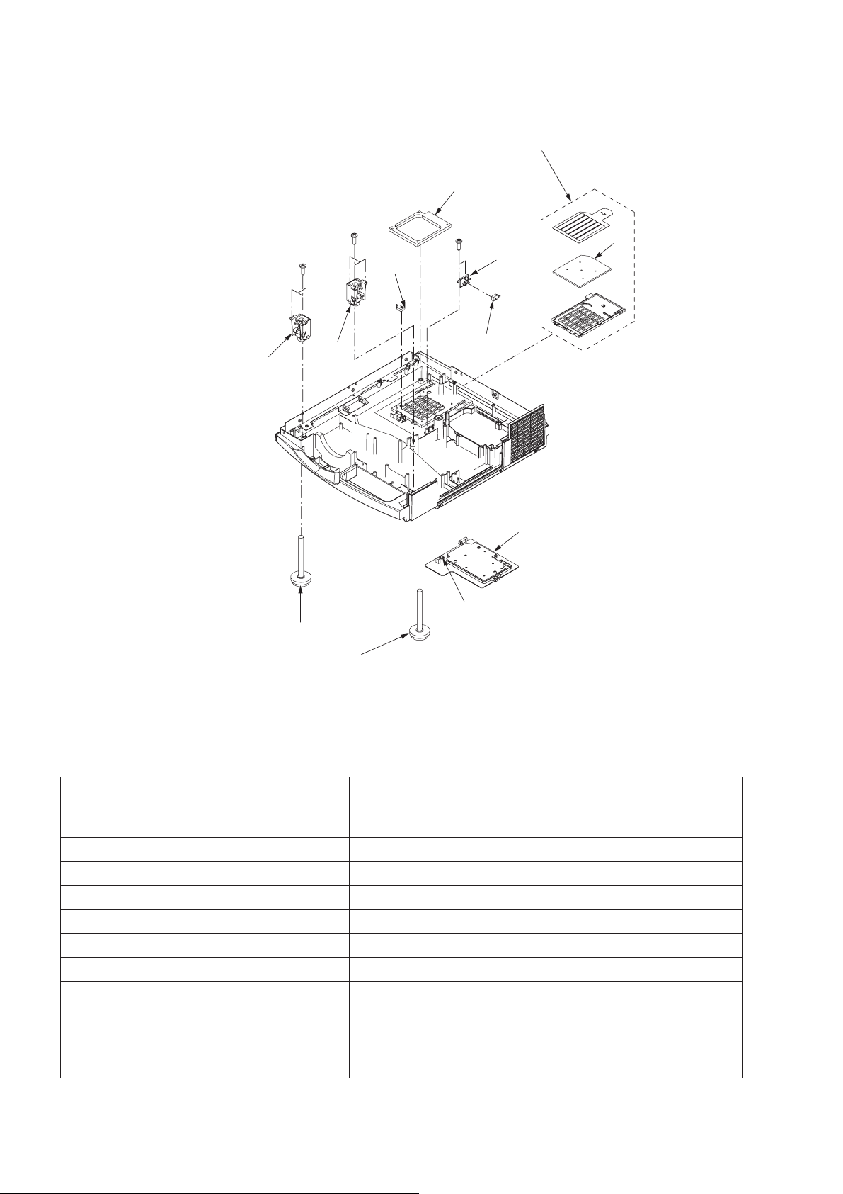
EXPOSED VIEW
A
L VP ASSY
Hx3
Jx3
11
13
12
Kx3
Lx4
14
Mx2
1
x6
Dx2
2
3
Cx4
Gx2
Ex2
6
5
10
Fx1
7
8
9
4
Bx3
Fig.2-1
- 6 -
Page 12

Parts list : See page 3 of PARTS LIST
Part name Number of screw
1.Front case ASSY None
2.Lens cap None
3.Front case unit Ax6
4.Terminal cover unit Bx3
5.Alarm unit ASSY Cx4
6.Alarm cover U Dx2
7.BOO PCB ASSY Ex2
8.BOO SUB PCB ASSY Fx1
9.Alarm cover L None
10.Sensor Gx2
11.Top case ASSY None
12.Top cover unit Hx3
13.Top case unit Jx3,Kx3,Lx4
14.KEY PCB ASSY Mx2
Table 2-1
- 7 -
Page 13
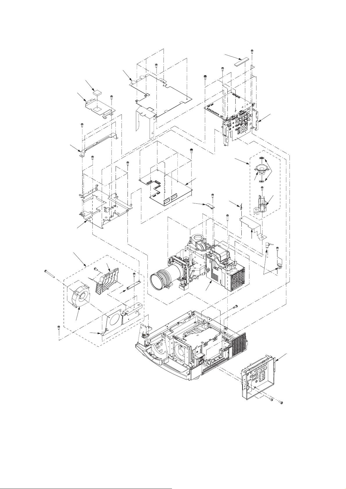
Chassis 1 ASSY
Cx5
2
5
Dx3
3
Fx3
Ex3
6
Hx2
7
9
10
Kx2
Gx1
Lx4
15
Jx8
8
Rx1
20
Ux5
16
21
17
4
18
Sx1
19
Tx2
Nx3
Mx2
12
Px3
11
13
14
Qx1
Fig.2-2
23
Vx1
22
Bx2
1
Ax1
- 8 -
Page 14

Parts list : See page 4 of PARTS LIST
Part name Number of screw
1.Terminal board unit Ax1,Bx2
2.Main barrier Cx5
3.Spacer cushion None
4.T erminal ASSY Dx3,Ex3,Fx3
5.Gum spacer None
6.Main radiator Gx1
7.Main PCB holder Hx2
8.DRIVE PCB ASSY Jx8
9.Drive PCB holder Kx2,Lx4
10.Drive fan ASSY None
11.Fan holder L Mx2
12.Drive fan Nx3
13.Fan PCB duct Px3
14.Shield holder Qx1
15.IRR PCB ASSY Rx1
16.Speaker ASSY None
17.Speaker None
18.Bush SP None
19.Holder SP Sx1
20.Lead clamper None
21.Thermo barrier None
22.Lamp power lead Tx2
23.Optical unit Ux5,Vx1
Table 2-2
- 9 -
Page 15
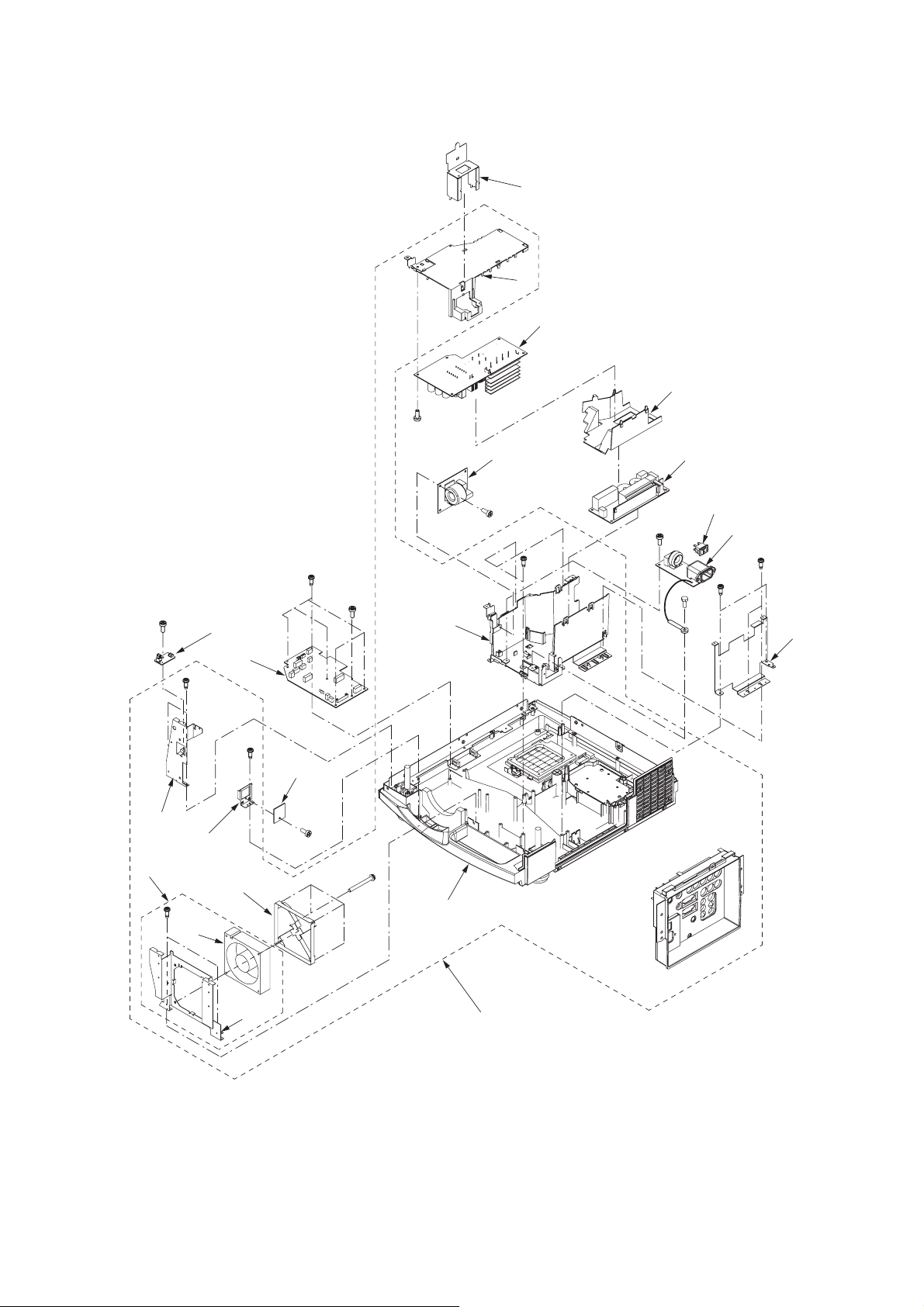
Chassis 2 ASSY
Lx1
17
12
13
14
15
16
Ax1
6
Mx1
Nx1
Gx5
Hx1
2
10
Bx2
Cx1
5
3
4
9
Ex2
8
Dx1
Fx4
20
21
Qx3
18
19
Kx2
Jx2
Px1
11
7
1
Fig.2-3
- 10 -
Page 16

Parts list : See page 5 of PARTS LIST
Part name Number of screw
1.Bottom case ASSY None
2.IRF PCB ASSY Ax1
3.Front holder L Bx2
4.Motor PCB holder Cx1
5.MOTOR PCB ASSY Dx1
6.Power fan ASSY None
7.Fan holder F Ex2
8.Power fan Fx4
9.Fan guard None
10.POWER SUB PCB ASSY Gx5,Hx1
11.Power shield L Jx2,Kx2
12.SW shield None
13.Power box T unit None
14.POWER PCB ASSY Lx1
15.Power fi n None
16.Lamp power unit None
17.FILTER PCB ASSY Mx1
18.Seesaw switch None
19.INLET PCB ASSY Nx1,Px1
20.Power box B unit Qx3
21.Bottom case unit None
Table 2-3
- 11 -
Page 17
Bottom case unit
Cx3
Dx3
1
4
Bx2
7
5
2
8
9
10
11
Fig.2-4
6
3
Ax1
Parts list : See page 6 of PARTS LIST
Part name Number of screw
1.Filter unit None
2.Fan fi lter None
3.Lamp cover unit Ax1
4.Fan cushion None
5.SW holder Bx2
6.Micro SW None
7.Micro SW None
8.Adjustment foot ASSY Cx3
9.Adjustment foot ASSY Dx3
10.Adiuster unit None
11.Adiuster unit None
Table 2-4
- 12 -
Page 18
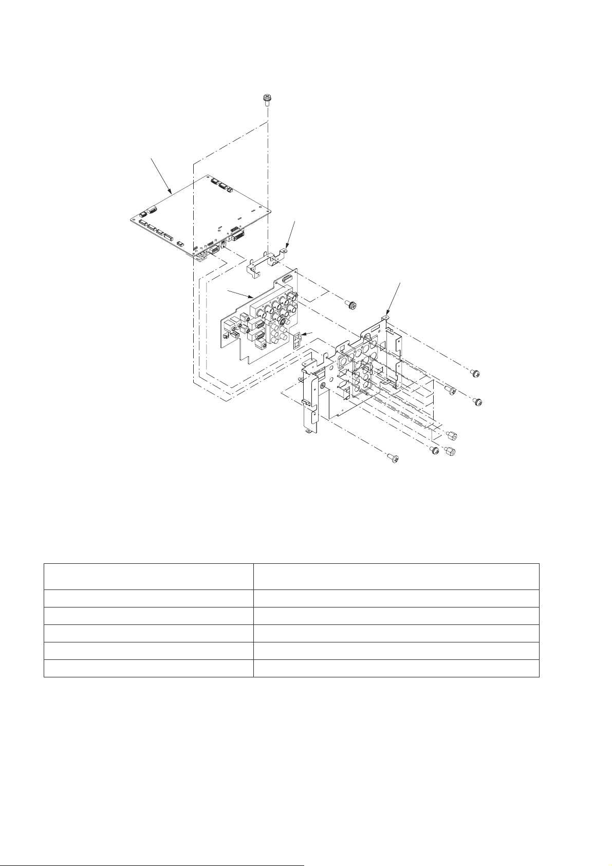
T erminal ASSY
Ax2
1
5
2
4
3
Jx2
Fx1
Fig.2-5
Parts list : See page 6 of PARTS LIST
Part name Number of screw
1.MAIN PCB ASSY Ax2,Bx4,Cx1
2.Terminal holder Dx8,Ex4,Fx1,Gx1,Hx1
3.Pin jack shield None
4.TERMINAL PCB ASSY Jx2
5.PCB holder None
Cx1
Hx1
Gx1
Dx8
Bx4
Ex4
Table 2-5
- 13 -
Page 19
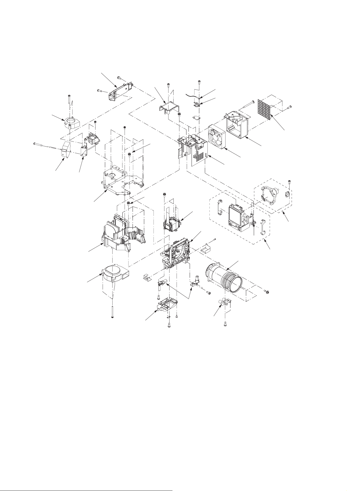
Optical unit 1
Fx2
1
Ex2
5
6
Bx1
7
12
Gx2
Ax1
Lx6
Nx4
Cx2 Dx2
2
Mx2
Qx3
Kx3
15
22
3
4
11
Jx2
10
Hx4
8
9
Sx1
17
Rx2
14
13
Px3
21
Wx2
Zx1
Yx1
Fig.2-6
20
Vx2
16
18
Tx4
19
Ux2
- 14 -
Page 20

Parts list : See page 7 of PARTS LIST
Part name Number of screw
1.Lamp duct Ax1,Bx1
2.Lamp cover T duct Cx2
3.Thermistor Dx1
4.Thermostat Dx2
5.PBS fan Ex2
6.Lamp fan Fx2
7.PBS duct Gx2
8.Grille Hx4
9.Exhaust duct Jx2
10.Exhaust fan None
11.Lamp cover T Kx3
12.Sub frame cover Lx6,Mx2
13.Sub frame Nx4
14.LCD fan Px3
15.LCD block Qx3
16.Lamp case ASSY Rx2
17.Lamp Sx1
18.Lens unit Tx4
19.Zoom focus motor Ux2
20.Lens shift motor Vx2,Wx2
21.LCD duct Yx1,Zx1
22.Main F shift base None
Table 2-6
- 15 -
Page 21
Optical unit 2
Fx1
Jx1
Kx1
12
Gx1
1
2
9
Ax2
3
11
Hx1
8
10
Ex1
7
Cx1
Dx1
6
5
1
Bx
4
Fig.2-7
Dlrections which the setting parts face in
Light source side(Lamp side)
123 7,8,9 10,11,12
Flat surface
Marking Color marking
Shaved edge
Uneven surface
Flat surface Flat surface
In possible
directions
Convex
Projection side(Lamp side)
4,5,6
Surface to stick
the polarizer on
Color marking
4,7,10 :
5,8,11 :
6,9,12 :
- 16 -
Surface to stick
the polarizer on
Color marking Color marking
Flat surface Flat surface
Surface to stick
the polarizer on
Blue
Green
Red
Page 22

Parts list : See page 8 of PARTS LIST
A
Part name Number of screw
1.PBS ASSY None
2.Multi lens B None
3.Multi lens A Ax2
4.Polarizer (B) IN Bx1
5.Polarizer (G) IN Cx1
6.Polarizer (R) IN Dx1
7.Polarizer (B) OUT Ex1
8.Polarizer (G) OUT Fx1
9.Polarizer (R) OUT Gx1
10.Polarizer (B) PURI Hx1
11.Polarizer (G) PURI Jx1
12.Polarizer (R) PURI Kx1
Table 2-7
POSITION ADJUSTMENT OF MULTI LENS A
Follow the steps below for the adjustment after replacing the
multi lens A.
Number of jig screw : 859C746O10
1. Fasten two screws (a) to secure the Multi lens A
temporarily.
2. Project a full white raster on the screen.
3. Adjust the position of the multi lens A to correct color
unevenness near the screen edges.
To adjust the vertical position, turn the screw (b).
To adjust the horizontal position, use the jig screw (c).
4. Fasten two screws (a) and two screws (d) tightly to
secure the Multi Lens A fi rmly.
ax2
b
d
x2
Multi lens
c
- 17 -
Page 23
DISASSEMBLY
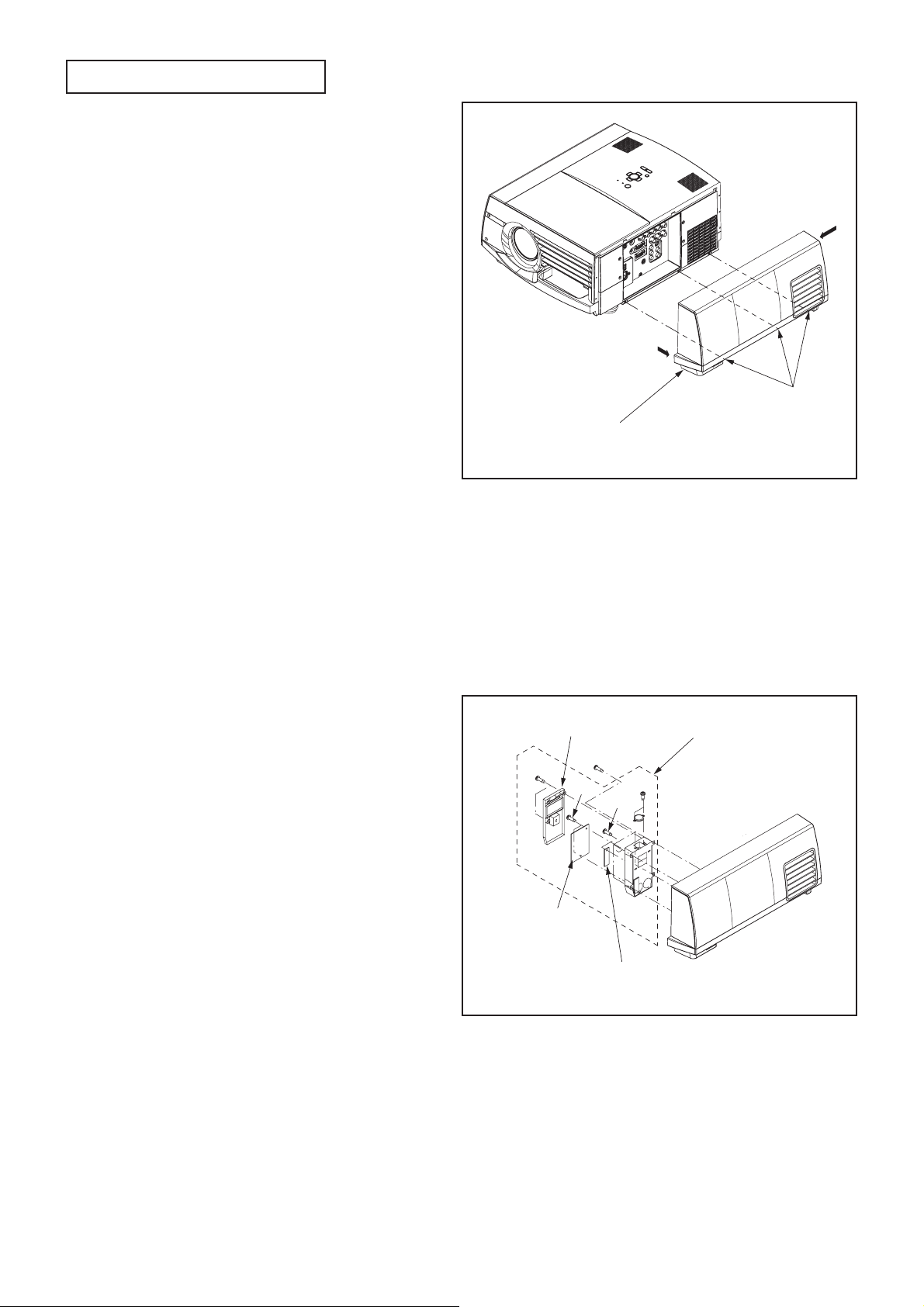
1. Removal of the terminal cover ASSY
1. Loosen the three screws (a) as shown in Fig. 3-1.
2. Open the bottom of the terminal cover ASSY outward
(as shown by the arrow (A)) as shown in Fig. 3-1.
3. Slide the top of the terminal cover ASSY to the front
for removal (as shown by the arrow (B)) as shown in
Fig. 3-1.
B
A
ax3
Terminal cover ASSY
Fig. 3-1
2. Removal of the BOO PCB ASSY and BOO SUB PCB ASSY
1. Remove the terminal cover ASSY according to “1.
Remove of the terminal cover ASSY”.
2. Remove the four screws (a) as shown in Fig. 3-2.
3. Remove the alarm unit ASSY as shown in Fig. 3-2.
4. Remove the two screws (b) as shown in Fig. 3-2.
5. Remove the alarm cover U as shown in Fig. 3-2.
6. Remove the two screws (c) as shown in Fig. 3-2.
7. Remove the BOO PCB ASSY as shown in Fig. 3-2.
8. Remove the screw (d) as shown in Fig. 3-2.
9. Remove the BOO SUB PCB ASSY as shown in Fig.
3-2.
Alarm cover U
bx2
BOO PCB ASSY
ax4
cx2
BOO SUB PCB ASSY
Alarm unit ASSY
dx1
Fig. 3-2
- 18 -
Page 24

3. Removal of the lens unit and zoom focus motor
1. Remove the six screws (a) as shown in Fig. 3-3.
2. Pull the top and left side of the front case unit (as
shown by the arrow (A)) as shown in Fig. 3-3.
3. Raise the left side of the front case unit (as shown by
the arrow (B)) as shown in Fig. 3-3.
4. Pull the left side of the front case unit to front for re-
moval (as shown by the arrow (c)) as shown in Fig.
3-3.
5. Remove the three screws (b) as shown in Fig. 3-3.
6. Slide the top cover unit to the front (as shown by ar-
row (D)) as shown in Fig. 3-3.
7. Remove the top cover unit to upward (as shown by
the arrow (E)) as shown Fig. 3-3.
8. Disconnect the connector (MA) as shown in Fig. 3-3.
9. Loosen the four screws (c) as shown in Fig. 3-3.
10. Remove the lens unit as shown Fig. 3-3.
11. Remove the two screws (d) as shown in Fig. 3-3.
12. Remove the zoom focus motor as shown in Fig. 3-3.
Top cover unit
D
E
bx3
Lens unit
cx4
Zoom focus motor
dx2
ax6
A B
C
Fig. 3-3
MA
Front case unit
- 19 -
Page 25
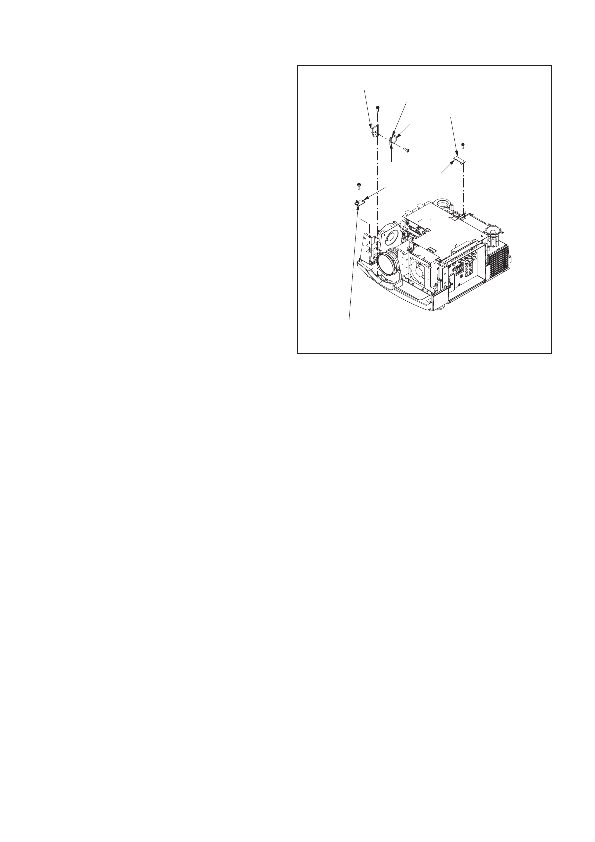
4. Removal of the top case unit and KEY PCB ASSY
1. Remove the terminal cover ASSY according to “1.
Removal of the terminal cover ASSY”.
2. Remove the front case unit and top cover unit ac-
cording to “3. Removal of the lens unit and zoom focus motor”.
3. Remove the three screws (a), three screws (b) and
four screws (c) as shown in Fig. 3-4.
4. Disconnect the connector (ST) as shown in Fig. 3-4.
5. Remove the top case unit as shown in Fig. 3-4.
6. Remove the two screws (d) as shown in Fig. 3-4.
7. Remove the KEY PCB ASSY as shown in Fig. 3-4.
ax3
Top case unit
KEY PCB ASSY
ST
bx3
cx4
dx2
Fig. 3-4
- 20 -
Page 26
5. Removal of the IRF PCB ASSY
1. Remove the terminal cover ASSY according to “1.
Removal of the terminal cover ASSY”.
2. Remove the front case unit and top cover unit ac-
cording to “3. Removal of the lens unit and zoom focus motor”.
3. Remove the top case unit according to “4. Removal
of the top case unit and KEY PCB ASSY”.
4. Remove the screw (a) as shown in Fig. 3-5
5. Disconnect the connector (AM) as shown in Fig. 3-5
6. Remove the IRF PCB ASSY as shown in Fig. 3-5.
6. Removal of the MOTOR PCB ASSY
1. Remove the terminal cover ASSY according to “1.
Removal of the terminal cover ASSY”.
2. Remove the front case unit and top cover unit ac-
cording to “3. Removal of the lens unit and zoom focus motor”.
3. Remove the top case unit according to “4. Removal
of the top case unit and KEY PCB ASSY”.
4. Remove the screw (b) as shown in Fig. 3-5.
5. Remove the motor PCB holder as shown in Fig. 3-5.
6. Remove the screw (c) as shown in Fig. 3-5.
7. Disconnect the two connectors (MA and MV) as
shown in Fig. 3-5.
8. Remove the MOTOR PCB ASSY as shown in Fig.
3-5.
Motor PCB holder
MOTOR PCB ASSY
bx1
ax1
IRF PCB ASSY
MV
AM
MA
cx1
Fig. 3-5
IRR PCB ASSY
dx1
AL
7. Removal of the IRR PCB ASSY
1. Remove the terminal cover ASSY according to “1.
Removal of the terminal cover ASSY”.
2. Remove the front case unit and top cover unit ac-
cording to “3. Removal of the lens unit and zoom focus motor”.
3. Remove the top case unit according to “4. Removal
of the top case unit and KEY PCB ASSY”.
4. Removal the screw (d) as shown in Fig. 3-5.
5. Disconnect the connector (AL) as shown in Fig. 3-5.
6. Remove the IRR PCB ASSY as shown in Fig. 3-5.
- 21 -
Page 27
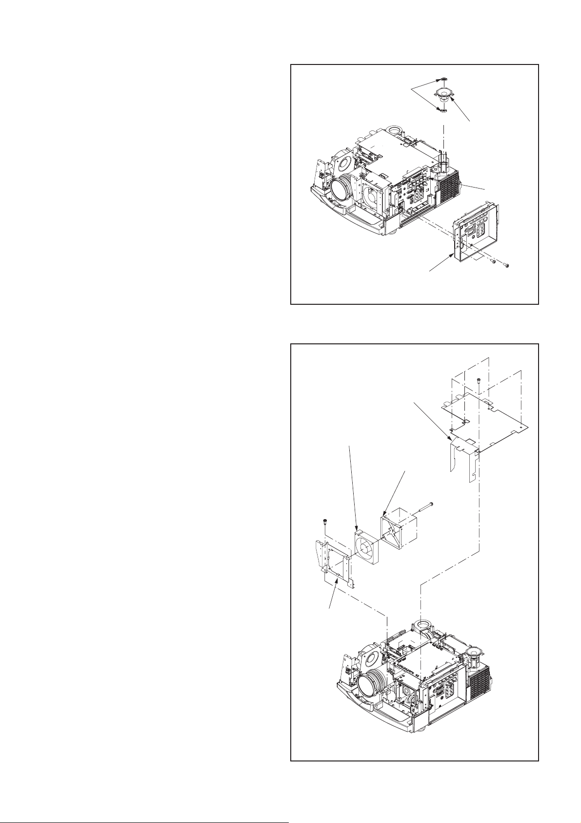
8. Removal of the speaker
1. Remove the terminal cover ASSY according to “1.
Removal of the terminal cover ASSY”.
2. Remove the front case unit and top cover unit ac-
cording to “3. Removal of the lens unit and zoom focus motor”.
3. Remove the top case unit according to “4. Removal
of the top case unit and KEY PCB ASSY”.
4. Remove the two screws (a) and screw (b) as shown
in Fig. 3-6.
5. Remove the terminal board unit as shown in Fig. 3-6.
6. Disconnect the connector (TL) as shown in Fig. 3-6.
7. Remove the bush SP as shown in Fig. 3-6.
8. Remove the speaker as shown in Fig. 3-6.
9. Removal of the power fan
1. Remove the terminal cover ASSY according to “1.
Removal of the terminal cover ASSY”.
2. Remove the front case unit and top cover unit ac-
cording to “3. Removal of the lens unit and zoom focus motor”.
3. Remove the top case unit according to “4. Removal
of the top case unit and KEY PCB ASSY”.
4. Remove the fi ve screws (a) as shown in Fig. 3-7.
5. Remove the main barrier as shown in Fig. 3-7
6. Remove the two screws (b) as shown in Fig. 3.-7.
7. Remove the fan holder F as shown in Fig. 3-7.
8. Remove the four screws (c) as shown in Fig. 3-7.
9. Remove the fan guard and power fan as shown in
Fig. 3-7.
Power fan
bx2
Bush SP
Terminal board unit
Fig. 3-6
Main barrier
Fan guard
Speaker
TL
bx1
ax2
ax5
cx4
- 22 -
Fan holder F
Fig. 3-7
Page 28
10. Removal of the MAIN PCB ASSY
1. Remove the terminal cover ASSY according to “1.
Removal of the terminal cover ASSY”.
2. Remove the front case unit and top cover unit ac-
cording to “3. Removal of the lens unit and zoom focus motor”.
3. Remove the top case unit according to “4. Removal
of the top case unit and KEY PCB ASSY”.
4. Remove the terminal board unit according to “8. Re-
moval of the speaker”.
5. Remove the main barrier according to “9. Removal of
the power fan”.
6. Remove the three screws (a), two screws (b), four
screws (c) and screw (d) as shown in Fig. 3-8.
7. Disconnect the connectors (SA, SC,SD, SE, SF, SL,
SQ, SX and SZ) as shown in Fig. 3-8.
8. Remove the MAIN PCB ASSY as shown in Fig. 3-8.
Note: The DV-SV connector, DW-SW connector and SK-TK
connector are connected directly each other.
Disconnect these connectors before removing the
MAIN PCB ASSY.
ax3
SQ
SF
SC
SE
TERMINAL
PCB ASSY
SD
SV SW
SA
SL
TW
bx2
SZ
MAIN PCB ASSY
SX
SK
PCB holder
TK
TL
nx2
T erminal ASSY
ex3
dx1
fx3
mx1
gx8
hx4
jx1
kx1
cx4
11. Removal of the TERMINAL PCB
ASSY
1. Remove the terminal cover ASSY according to “1.
Removal of the terminal cover ASSY”.
2. Remove the front case unit and top cover unit ac-
cording to “3. Removal of the lens unit and zoom focus motor”.
3. Remove the top case unit according to “4. Removal
of the top case unit and KEY PCB ASSY”.
4. Remove the terminal board unit according to “8. Re-
moval of the speaker”.
5. Remove the main barrier according to “9. Removal of
the power fan”.
6. Remove the three screws (a), three screws (e) and
three screws (f) as shown in Fig.3-8.
7. Disconnect the connectors (SA, SC, SD, SE,SF, SL,
SQ, SX, SZ, TL and TW) as shown in Fig. 3-8.
8. Remove the terminal ASSY as shown in Fig. 3-8.
Note: The DV-SV connector and DW-SW connector are
connected directly each other.
Disconnect these connectors before removing the
terminal ASSY .
9. Remove the two screws (b), four screws (c), screw (d),
eight screws (g), four screws (h), screw (j), screw (k)
and screw (m) as shown in Fig. 3-8.
10. Remove the MAIN PCB ASSY and terminal holder as
shown in Fig. 3-8.
Note: The SK-TK connector are connected directly each
other.
Disconnect these connectors before removing the
MAIN PCB ASSY.
11. Remove the two screws (n) as shown Fig. 3-8.
12. Remove the TERMINAL PCB ASSY as shown Fig.
3-8.
DWDV
Fig. 3-8
Terminal holder
- 23 -
Page 29

Y
12. Removal of the DRIVE PCB
ASSY and LCD block
1. Remove the terminal cover ASSY according to “1.
Removal of the terminal cover ASSY”.
2. Remove the front case unit and top cover unit ac-
cording to “3. Removal of the lens unit and zoom focus motor”.
3. Remove the top case unit according to “4. Removal
of the top case unit and KEY PCB ASSY”.
4. Remove the terminal board unit according to “8. Re-
moval of the speaker”.
5. Remove the main barrier according to “9. Removal of
the power fan”.
6. Remove the terminal ASSY according to “11. Remov-
al of the TERMINAL PCB ASSY”.
7. Remove the screw (a) as shown in Fig. 3-9.
8. Remove the main radiator as shown in Fig. 3-9.
9. Remove the two screws (b) as shown in Fig. 3-9.
10. Remove the main PCB holder as shown in Fig. 3-9.
11. Remove the eight screws (c) as shown in Fig. 3-9.
12. Disconnect the connectors (DB, DG, DP and DR) as
shown in Fig. 3-9.
13. Remove the DRIVE PCB ASSY as shown in Fig. 3-9.
14. Remove the three screws (d) as shown in Fig. 3-9.
15. Remove the LCD block as shown in Fig. 3-9.
Main PCB holder
bx2
DR
DP
LCD block
Main radiator
ax1
DG
cx8
DB
dx3
DRIVE PCB ASS
Fig. 3-9
- 24 -
Page 30

13. Removal of the drive fan
1. Remove the terminal cover ASSY according to “1.
Removal of the terminal cover ASSY”.
2. Remove the front case unit and top cover unit ac-
cording to “3. Removal of the lens unit and zoom focus motor”.
3. Remove the top case unit according to “4. Removal
of the top case unit and KEY PCB ASSY”.
4. Remove the terminal board unit according to “8. Re-
moval of the speaker”.
5. Remove the main barrier according to “9. Removal of
the power fan”.
6. Remove the terminal ASSY according to “11. Remov-
al of the TERMINAL PCB ASSY”.
7. Remove the DRIVE PCB ASSY according to “12. Re-
moval of the DRIVE PCB ASSY and LCD block ”.
8. Remove the two screws (a) and four screws (b) as
shown in Fig. 3-10.
9. Remove the drive PCB holder as shown in Fig. 3-10.
10. Remove the two screws (C) as shown in Fig. 3-10.
11. Disconnect the connector (ND) as shown in Fig. 3-10.
12. Remove the fan holder L as shown in Fig. 3-10.
13. Remove the three screws (d) as shown in Fig. 3-10.
14. Remove the drive fan as shown in Fig. 3-10.
PBS fan
cx2
Drive PCB holder
ax2
ex2
ND
bx4
NB
14. Removal of the PBS fan
1. Remove the terminal cover ASSY according to “1.
Removal of the terminal cover ASSY”.
2. Remove the front case unit and top cover unit ac-
cording to “3. Removal of the lens unit and zoom focus motor”.
3. Remove the top case unit according to “4. Removal
of the top case unit and KEY PCB ASSY”.
4. Remove the terminal board unit according to “8. Re-
moval of the speaker”.
5. Remove the main barrier according to “9. Removal of
the power fan”.
6. Remove the terminal ASSY according to “11. Remov-
al of the TERMINAL PCB ASSY”.
7. Remove the DRIVE PCB ASSY according to “12. Re-
moval of the DRIVE PCB ASSY and LCD block ”.
8. Remove the fan holder L according to “13. Removal
of the drive fan”.
9. Remove the two screws (e) as shown in Fig. 3-10.
10. Disconnect the connector (NB) as shown in Fig. 3-10.
11. Remove the PBS fan as shown in Fig. 3-10.
dx3
Fan holder L
Drive fan
Fig. 3-10
- 25 -
Page 31

15. Removal of the optical unit
1. Remove the terminal cover ASSY according to “1.
Removal of the terminal cover ASSY”.
2. Remove the front case unit and top cover unit ac-
cording to “3. Removal of the lens unit and zoom focus motor”.
3. Remove the top case unit according to “4. Removal
of the top case unit and KEY PCB ASSY”.
4. Remove the IRR PCB ASSY according to “7. Remov-
al of the IRR PCB ASSY”.
5. Remove the speaker according to “8. Removal of the
speaker”.
6. Remove the main barrier according to “9. Removal of
the power fan”.
7. Remove the terminal ASSY according to “11. Remov-
al of the TERMINAL PCB ASSY”.
8. Remove the DRIVE PCB ASSY according to “12. Re-
moval of the DRIVE PCB ASSY and LCD block”.
9. Remove the fan holder L according to “13. Removal
of the drive fan”.
10. Remove the screw (a) as shown in Fig. 3-11.
11. Remove the holder SP, lead clamper and thermo bar-
rier as shown in Fig. 3-11.
12. Remove the two screws (b) as shown in Fig. 3-11.
13. Disconnect the lamp power lead and thermostat con-
nector as shown in Fig. 3-11.
14. Remove the fi ve screws (c) and screws (d) shown in
Fig. 3-11.
15. Disconnect the connectors (MA, NB, NK, NR, and
NS) as shown in Fig. 3-11.
16. Remove the optical unit as shown in Fig. 3-11.
Thermo barrier
Optical unit
NB
NR
MA
Holder SP
Lead clamper
NK
NS
cx5
ax1
dx1
bx2
Lamp power
lead
Thermostat
connector
Fig. 3-11
- 26 -
Page 32

16. Removal of the POWER PCB
ASSY
1. Remove the terminal cover ASSY according to “1.
Removal of the terminal cover ASSY”.
2. Remove the front case unit and top cover unit ac-
cording to “3. Removal of the lens unit and zoom focus motor”.
3. Remove the top case unit according to “4. Removal
of the top case unit and KEY PCB ASSY”.
4. Remove the terminal board unit according to “8. Re-
moval of the speaker”.
5. Remove the main barrier according to “9. Removal of
the power fan”.
6. Remove the terminal ASSY according to “11. Remov-
al of the TERMINAL PCB ASSY”.
7. Remove the DRIVE PCB ASSY according to “12. Re-
moval of the DRIVE PCB ASSY and LCD block ”.
8. Remove the drive PCB holder according to “13. Re-
moval of the drive fan”.
9. Disconnect the thermostat connector according to “15.
Removal of the optical unit”.
10. Remove the two screws (a) and two screws (b) as
shown in Fig. 3-12.
11. Remove the power shield L and SW shield as shown
in Fig. 3-12.
12. Release the three hook (c) as shown in Fig. 3-12.
13. Lift the power box T unit and disconnect the connec-
tor (RD, RF and RH) as shown in Fig. 3-12.
14. Remove the power box T unit as shown in Fig. 3-12.
15. Remove the screw (d) as shown in Fig.3-12.
16. Release the three hook (e) as shown in Fig. 3-12.
17. Remove the POWER PCB ASSY as shown in Fig.
3-12.
POWER PCB ASSY
RH
dx1
Fig. 3-12
SW shield
Power box T unit
bx2
ex3
RF
RD
Power shield L
cx3
ax2
- 27 -
Page 33

17. Removal of the lamp power unit
Y
1. Remove the terminal cover ASSY according to “1.
Removal of the terminal cover ASSY”.
2. Remove the front case unit and top cover unit ac-
cording to “3. Removal of the lens unit and zoom focus motor”.
3. Remove the top case unit according to “4. Removal
of the top case unit and KEY PCB ASSY”.
4. Remove the tspeaker according to “8. Removal of the
speaker”.
5. Remove the main barrier according to “9. Removal of
the power fan”.
6. Remove the terminal ASSY according to “11. Remov-
al of the TERMINAL PCB ASSY”.
7. Remove the DRIVE PCB ASSY according to “12. Re-
moval of the DRIVE PCB ASSY and LCD block ”.
8. Remove the drive PCB holder according to “13. Re-
moval of the drive fan”.
9. Disconnect the lamp power lead and thermostat con-
nector according to “15. Removal of the optical unit”.
10. Remove the power box T unit according to “16. Re-
moval of the POWER PCB ASSY”.
11. Remove the power fi n as shown in Fig. 3-13.
12. Release the two hook (a) as shown in Fig. 3-13.
13. Remove the lamp power unit as shown in Fig. 3-13.
Power fin
Lamp power unit
ax2
Fig. 3-13
18. Removal of the FILTER PCB
ASSY and INLET PCB ASSY
1. Remove the terminal cover ASSY according to “1.
Removal of the terminal cover ASSY”.
2. Remove the front case unit and top cover unit ac-
cording to “3. Removal of the lens unit and zoom focus motor”.
3. Remove the top case unit according to “4. Removal
of the top case unit and KEY PCB ASSY”.
4. Remove the speaker according to “8. Removal of the
speaker”.
5. Remove the main barrier according to “9. Removal of
the power fan”.
6. Remove the terminal ASSY according to “11. Remov-
al of the TERMINAL PCB ASSY”.
7. Remove the DRIVE PCB ASSY according to “12. Re-
moval of the DRIVE PCB ASSY and LCD block ”.
8. Remove the drive PCB holder according to “13. Re-
moval of the drive fan”.
9. Disconnect the lamp power lead and thermostat con-
nector according to “15. Removal of the optical unit”.
10. Remove the power box T unit according to “16. Re-
moval of the POWER PCB ASSY”.
11. Remove the screw (a) as shown in Fig. 3-14.
12. Lift the FILTER PCB ASSY and disconnect the con-
nector (PP) as shown in Fig. 3-14.
13. Remove the FILTER PCB ASSY as shown in Fig.
3-14.
14. Remove the screw (b) and screw (c) as shown in
Fig.-3-14.
15. Remove the INLET PCB ASSY as shown in Fig.
3-14.
INLET PCB ASSY
bx1
FILTER PCB ASS
cx1
ax1
PP
Fig. 3-14
- 28 -
Page 34

Y
19. Removal of the POWER SUB
PCB ASSY
1. Remove the terminal cover ASSY according to “1.
Removal of the terminal cover ASSY”.
2. Remove the front case unit and top cover unit ac-
cording to “3. Removal of the lens unit and zoom focus motor”.
3. Remove the top case unit according to “4. Removal
of the top case unit and KEY PCB ASSY”.
4. Remove the IRR PCB ASSY according to “7. Remov-
al of the IRR PCB ASSY”.
5. Remove the speaker according to “8. Removal of the
speaker”.
6. Remove the main barrier according to “9. Removal of
the power fan”.
7. Remove the terminal ASSY according to “11. Remov-
al of the TERMINAL PCB ASSY”.
8. Remove the DRIVE PCB ASSY according to “12. Re-
moval of the DRIVE PCB ASSY and LCD block”.
9. Remove the fan holder L according to “13. Removal
of the drive fan”.
10. Remove the optical unit according to “15. Removal of
the optical unit”.
1 1. Remove the fi ve screws (a) and screw (b) as shown
in Fig. 3-15.
12. Disconnect the connectors (NA, NH, NM, NV) as
shown in Fig. 3-15.
13. Remove the POWER SUB ASSY as shown Fig. 3-15.
NM
NV
ax5
bx1
POWER SUB PCB ASS
NH
NA
Fig. 3-15
- 29 -
Page 35

20. Removal of the lamp fan
1. Remove the terminal cover ASSY according to “1.
Removal of the terminal cover ASSY”.
2. Remove the front case unit and top cover unit ac-
cording to “3. Removal of the lens unit and zoom focus motor”.
3. Remove the top case unit according to “4. Removal
of the top case unit and KEY PCB ASSY”.
4. Remove the IRR PCB ASSY according to “7. Remov-
al of the IRR PCB ASSY”.
5. Remove the speaker according to “8. Removal of the
speaker”.
6. Remove the main barrier according to “9. Removal of
the power fan”.
7. Remove the terminal ASSY according to “11. Remov-
al of the TERMINAL PCB ASSY”.
8. Remove the DRIVE PCB ASSY according to “12. Re-
moval of the DRIVE PCB ASSY and LCD block”.
9. Remove the fan holder L according to “13. Removal
of the drive fan”.
10. Remove the optical unit according to “15. Removal of
the optical unit”.
11. Remove the two screws (a) as shown in Fig. 3-16.
12. Remove the lamp fan as shown in Fig. 3-16.
Lamp fan
ax2
LCD fan
bx3
Fig. 3-16
21. Removal of the LCD fan
1. Remove the terminal cover ASSY according to “1.
Removal of the terminal cover ASSY”.
2. Remove the front case unit and top cover unit ac-
cording to “3. Removal of the lens unit and zoom focus motor”.
3. Remove the top case unit according to “4. Removal
of the top case unit and KEY PCB ASSY”.
4. Remove the IRR PCB ASSY according to “7. Remov-
al of the IRR PCB ASSY”.
5. Remove the speaker according to “8. Removal of the
speaker”.
6. Remove the main barrier according to “9. Removal of
the power fan”.
7. Remove the terminal ASSY according to “11. Remov-
al of the TERMINAL PCB ASSY”.
8. Remove the DRIVE PCB ASSY according to “12. Re-
moval of the DRIVE PCB ASSY and LCD block”.
9. Remove the fan holder L according to “13. Removal
of the drive fan”.
10. Remove the optical unit according to “15. Removal of
the optical unit”.
11. Remove the three screws (b) as shown in Fig. 3-16.
12. Remove the LCD fan as shown in Fig. 3-16.
- 30 -
Page 36

22. Removal of the exhaust fan
1. Remove the terminal cover ASSY according to “1.
Removal of the terminal cover ASSY”.
2. Remove the front case unit and top cover unit ac-
cording to “3. Removal of the lens unit and zoom focus motor”.
3. Remove the top case unit according to “4. Removal
of the top case unit and KEY PCB ASSY”.
4. Remove the IRR PCB ASSY according to “7. Remov-
al of the IRR PCB ASSY”.
5. Remove the speaker according to “8. Removal of the
speaker”.
6. Remove the main barrier according to “9. Removal of
the power fan”.
7. Remove the terminal ASSY according to “11. Remov-
al of the TERMINAL PCB ASSY”.
8. Remove the DRIVE PCB ASSY according to “12. Re-
moval of the DRIVE PCB ASSY and LCD block”.
9. Remove the fan holder L according to “13. Removal
of the drive fan”.
10. Remove the optical unit according to “15. Removal of
the optical unit”.
11. Remove the four screws (a) as shown in Fig.3-17.
12. Remove the grille as shown in Fig. 3-17.
13. Remove of the two screws (b) as show in Fig.3-17.
14. Remove of the exhaust dust and exhaust fan.
Grille
Exhaust fan
bx2
ax4
Exhaust duct
Fig. 3-17
23. Removal of the lens shift motor
1. Remove the terminal cover ASSY according to “1.
Removal of the terminal cover ASSY”.
2. Remove the front case unit and top cover unit ac-
cording to “3. Removal of the lens unit and zoom focus motor”.
3. Remove the top case unit according to “4. Removal
of the top case unit and KEY PCB ASSY”.
4. Remove the IRR PCB ASSY according to “7. Remov-
al of the IRR PCB ASSY”.
5. Remove the speaker according to “8. Removal of the
speaker”.
6. Remove the main barrier according to “9. Removal of
the power fan”.
7. Remove the terminal ASSY according to “11. Remov-
al of the TERMINAL PCB ASSY”.
8. Remove the DRIVE PCB ASSY according to “12. Re-
moval of the DRIVE PCB ASSY and LCD block”.
9. Remove the fan holder L according to “13. Removal
of the drive fan”.
10. Remove the optical unit according to “15. Removal of
the optical unit”.
11. Remove the two screws (a) and two screws (b) as
shown in Fig. 3-18.
12. Remove the lens shift motor as shown in Fig. 3-18.
Lens shift motor
ax2
bx2
Fig. 3-18
- 31 -
Page 37

24. Removal of the lamp box
1. Remove the terminal cover ASSY according to “1.
Removal of the terminal cover ASSY”.
2. Remove the front case unit and top cover unit ac-
cording to “3. Removal of the lens unit and zoom focus motor”.
3. Remove the top case unit according to “4. Removal
of the top case unit and KEY PCB ASSY”.
4. Remove the IRR PCB ASSY according to “7. Remov-
al of the IRR PCB ASSY”.
5. Remove the speaker according to “8. Removal of the
speaker”.
6. Remove the main barrier according to “9. Removal of
the power fan”.
7. Remove the terminal ASSY according to “11. Remov-
al of the TERMINAL PCB ASSY”.
8. Remove the DRIVE PCB ASSY according to “12. Re-
moval of the DRIVE PCB ASSY and LCD block”.
9. Remove the fan holder L according to “13. Removal
of the drive fan”.
10. Remove the optical unit according to “15. Removal of
the optical unit”.
11. Loosen the two screws (a) as shown in Fig. 3-19.
12. Remove the lamp box as shown in Fig. 3-19.
ax2
Lamp box
Fig. 3-19
LAMP REPLACEMENT
Note: Only service persons ore allowed to replace the lamp.
When replacing the lamp, be sure to wear gloves to
prevent the lamp from scratches and fi ngerprints that
can cause breakage of the lamp.
Removal
1. Remove the screw (a) and the power socket as
shown in Fig. 4-1.
2. Remove the side spring as shown in Fig. 4-1.
3. Remove the lamp as shown in Fig. 4-1.
Installation
1. Install the lamp in the reverse order of removal.
Note: Mount the lamp with the fl at area of the refl ect base
facing up.
Run the lead wire of the lamp so that it doesn't touch
the refl ector and the refl ect base.
Lamp
Side spring
Reflector
Power socket
Reflector base
ax1
Fig. 4-1
- 32 -
Page 38

LEAD DRESS
Note: The inner wires are clamped so that they do not come close to heat generating or high voltage parts. After servicin-
groute all wires in their original position.
Lead wire routing in the bottom case unit
Run the SL lead wire
outside this rib.
Clampe the SL lead
wire with the tape.
Run the SL lead wire
along the mark line.
±5
35
AL
SL
Connect the shorter SL lead wire here.
Connect the longer SL lead wire here.
Fig. 5-1
Lead wire routing after the POWER SUB PCB ASSY,
MOTOR PCB ASSY and power box B unit are attached
Power box B unit
POWER SUB PCB ASSY
MOTOR PCB ASSY
Run the NC,NE and NF lead wires
through the clamper.
NE
NV
NM
MV
NF
NC
Fig. 5-2
NP
NH
NW
Run the NC,NE,NF,NH and NP lead wires
through the clamper.
- 33 -
Page 39

Lead wire routing after the INLET PCB ASSY,
FILTER PCB ASSY, lamp power unit and power fan are attached
Lamp power unit
CN3
FILTER PCB ASSY
CN2
CN1
FL
PP
NA
Retain the NA and NW lead wires using the clamper.
FN
FG
Power fan
Clamp the FR,FS,FT and FU
lead wires after connecting them
to seesaw switch.
INLET PCB ASSY
Fig. 5-3
Lead wire routing after the POWER PCB ASSY and
IRF PCB ASSY are attached
FT
FR
FU
FS
Seesaw switch
AM
IRF PCB ASSY
RT2
RT1
RF
RD
RH
Run the AM lead wire
through the notch of the front holder L.
RE
Fig. 5-4
- 34 -
POWER PCB ASSY
Run the RE lead wire
through the hole of the power fin.
Page 40

Lead wire routing after the optical unit and
IRR PCB ASSY are attached
Run the SL lead wire
through the hook of
the optical unit.
Run the NB,NK,NR
and NS lead wires
through the two
clampers.
NB
IRR PCB ASSY
NK
NS
NR
AL
optical unit
Clamp the brown and red
lead wires with the band.
Run the thermostat
lead wires over the lamp
power lead wire.
MA
Fig. 5-5
- 35 -
Page 41

Lead wire routing after the drive fan and
DRIVE PCB ASSY are attached
Retain the SL,SX and SZ lead wires
using the clamper.
Remove slack in the SL lead wires
by pulling them in the arrow’ s direction.
DR
Drive fan
ND
Run the ND lead wire
through the clamper of fan holder L.
Retain the DP and SD lead wires
using the clamper.
DG
DRIVE PCB ASSY
DB
DP
Run the SC,SE and SF lead wires
through the clamper.
Fig. 5-6
- 36 -
Page 42

Lead wire routing after the speaker and
terminal ASSY are attached
Speaker
SX
SZ
SL
TL
Terminal ASSY
SD
SQ
SE
SC
SF
Run the TW lead wire
over the main barrier.
Fig. 5-7
Run the TL lead wire
through the hook of
the terminal holder.
SA
TW
Run the TW lead wire
through the upper hook of
the terminal holder.
Run the SA lead wire
through the two hooks of
the terminal holder.
- 37 -
Page 43

PACKING
10,11,12
13,14,15
16,17
10,18,19
20,21,22
9
6,7,8
Parts list : See page 9 of PARTS LIST
4,5
Item No. Part name
1 Packing case
2 Cushion T/B
3 Packing sheet
4 Fan fi lter
2
3
1
5 Packing bag
6 Terminal cover unit
7 Alarm unit ASSY
8 Packing sheet
9 Paking case
10 Packing bag
11 Quick reference
12 IB CD-ROM
13 Remote hand unit
14 Battery
15 Short pin plug
16 Ring
- 38 -
17 Ring B
18 Control cable
19 VGA cable
20 AC power cord (EU)
21 AC power cord (US)
22 AV cable
Page 44

LAMP REPLACEMENT
This projector is equipped with a lamp to project images. This lamp is a consumable. It may burn out or its brightness
may decrease during use. In such cases, replace the lamp with a new one as soon as possible. Be sure to replace the
lamp with a new lamp separately sold that is exclusive to this projector. Contact your dealer for purchase of the lamp.
Spare lamp VLT-XL6600LP
Warning:
• Be careful not to drop the lamp fi xing screws into the inside of the projector. Don’t put a metal piece or fl ammable
object into the projector. Using the projector with any foreign object present inside may result in electric shock or
fi re. When you can’t remove the foreign object from the inside, contact your dealer for removal.
• Be sure to install the lamp securely. When the lamp isn’t installed properly, it won’t illuminate. Improper installation
may also result in fi re.
• Don’t shake the removed lamp or don’t lift it above your face. You may be injured in your eye by fl ying or falling
glass fragments.
• Don’t replace the lamp immediately after use because the lamp cover is very hot. You may get burned. Turn off the
power using the POWER button. After the lamp goes out, wait about 2 minutes until the intake and exhaust fans
for cooling the lamp stop rotating. Then turn off the main power switch, unplug the power cord, and wait at least 1
hour to allow the lamp to cool down enough to the touch.
• Do not touch the lamp directly. It may break and cause injury or burn.
Interval of lamp replacement
The recommended interval of lamp replacement is about 4000 hours
depending on the operating environment and may be shorter than 4000 hours
*1*2
of consecutive use. Such interval differs
*1*2
. Decrease in luminescence and/or
color brightness indicates that the lamp needs to be replaced. When the lamp operation time exceeds 3000 hours*1,
the indicator will blink alternately between green and red (while the lamp is lit; when the lamp is not lit, the indicator
will be lit red only) and the lamp replacement message will appear on the screen for 1 minute everytime the lamp
is turned on. When the lamp has been used for about 3800 hours
will appear on the screen for 1 minute every 20 hours
*1*2
hours
, the projector automatically shuts off and can’t be used until the lamp is replaced and the lamp
*1
thereafter. When the lamp operation time exceeds 4000
*1
, the replacement message (LAMP EXCHANGE)
operation time is reset.
*1: Duration when LAMP MODE of the INSTALLATION menu is set to LOW. When it is set to STANDARD, this duration will be
shorted.
*2: When LAMP MODE is set to STANDARD, this duration will be shorted to 2000 hours.
Caution:
• Don’t remove the lamp for any purpose other than replacement. Unnecessary removal of the lamp may result in a
breakdown.
• This projector uses a high-pressure mercury lamp as the light source. The high-pressure mercury lamp may
explode or fail to illuminate permanently because of an impact, scratch, or deterioration through use. The period
of time until explosion or permanent failure to illuminate varies considerably from lamp to lamp, depending on
operation conditions. Therefore, the lamp may explode soon after the start of use.
• The possibility of explosion of the lamp increases if you use it beyond its replacement period. When the instruction
of lamp replacement appears, replace it with a new one immediately even if the lamp is still lighting normally.
• When the high-pressure mercury lamp explodes, glass fragments will scatter inside or outside the lamp box and
the gas charged inside the lamp will diffuse inside or outside the projector. The gas inside the lamp contains
mercury. Be careful not to breathe it or avoid it from entering your eye or mouth. If you should breathe it or if it
should enter your eye or mouth, see a doctor immediately.
• In the event that the high-pressure mercury lamp exploded, glass fragments may have been scattered inside the
projector. Ask your dealer to replace the lamp and to inspect the inside of the projector. When you clean or replace
the lamp by yourself, be sure to hold the handle of the lamp. You may get injured by glass fragments.
• Don’t replace the lamp while the projector is installed on the ceiling. Glass fragments may fall from the projector,
entering your eye or mouth causing injury.
• When placing the projector upside down to replace the lamp or conduct maintenance, ensure that the projector is
securely placed before working with it.
• Be sure to use the lamp exclusive to this projector, VLT-XL6600LP. Use of other lamps may cause a failure of the
projector.
- 1 -
Page 45

To replace the lamp:
(c)
(a)
(a)
Handle
(c)
1. Turn off the main power switch and unplug the power cord.
2. Reverse the projector gently.
3. Loosen the screw (a) using a Phillips screwdriver (+), and
remove the lamp cover (b).
4. Loosen the screws (c) using a Phillips screwdriver (+).
5. Pull up the handle.
6. Pull out the lamp box by the handle while holding the
(b)
projector.
• Pull the lamp box out of the projector slowly. If it is
pulled out quickly, the lamp may break scattering glass
fragments.
• Do not spill liquid on the removed lamp box or do not
place it near any fl ammable object or where children
can reach to prevent injury or fi re.
7. Load a new lamp box securely into the projector in the right
orientation.
8. Put the handle back to the original position.
• Make sure that the handle is locked.
9. Tighten up the screws (c) using a Phillips screwdriver (+).
10. Tighten up the screw (a) using a Phillips screwdriver (+) to
secure the lamp cover.
Reset of the lamp operation time
11. Plug the power cord into the wall outlet and turn on the
main power switch.
12. Hold down the W, X, and POWER buttons on the control
panel at the same time about 3 seconds.
Important:
• Unless these 3 buttons are held down at the same time, the lamp operation time isn’t reset.
• Make sure that the STATUS indicator is lit twice and the lamp operation time is reset successfully.
• The projector doesn’t turn on if the lamp cover isn’t attached securely.
• Be sure to reset the lamp operation time whenever you replace the lamp.
• Do not reset the lamp operation time unless you replace the lamp.
• The lamp is fragile. If it is broken, be careful not to cut yourself with glass fragments.
• Contact your dealer for a new lamp.
• This projector uses a lamp that contains mercury. Disposal of the lamp or the projector with the lamp may be
regulated due to environmental considerations. For disposal or recycling information, please contact your local
authorities or the Electronic Industries Alliance: www.eiae.org. (For the U.S. only.)
- 2 -
Page 46

MAINTENANCE
Warning:
• Never use fl ammable air duster or other materials when cleaning the air-fi lter. Flammable substances may ignite
causing fi re or backdown when the lamp is illuminated.
• Do not use fl ammable solvents (benzene, thinner, etc.) and fl ammable aerosols when cleaning the projector body
and lens. Flammable substances may ignite causing fi re or breakdown while the lamp is illuminating.
Caution:
Be sure to turn off the lamp and unplug the power cord from the wall outlet before you perform any maintenance on
the projector.
Cleaning of the air-fi lter
Clean the air-fi lter frequently (about once a month). If the fi lter or
ventilation grilles become clogged with dirt or dust, the temperature inside the projector may rise and cause troubles, such as
damage to the inside parts and shortening the life of the panels.
• When the temperature inside the projector rises, the STATUS
indicator will blink orange and the lamp will be turned off.
1. To remove the fi lter cover, slide the cover in the direction of the
arrow.
2. Remove the air-fi lter from the fi lter cover.
3. Wash the air-fi lter or change it with a new fi lter.
• Use water or diluted mild detergent to clean the fi lter. Rinse
the fi lter thoroughly and let it dry completely.
4. Attach the air-fi lter to the fi lter cover.
5. Attach the fi lter cover to the projector.
• Make sure that the air-fi lter is attached correctly without
displacement.
Important:
• If the fi lter is damaged or becomes extremely dirty, change it
with a new fi lter. Contact your dealer for a new fi lter.
• Use the dedicated fi lter only.
• The power will not turn on if the fi lter cover is improperly
installed.
Caution:
Be sure to use the projector with an air-fi lter. If not, dust may get inside the projector causing fi re and failure.
Filter cover
Filter cover
Air-fi lter
Cleaning of the projector and the ventilation slots
Use a soft cloth to clean the projector and the ventilation grilles. When the grilles become dirty, wipe them with a soft
cloth dampened with diluted mild detergent, and then wipe them with a dry cloth.
• Clean the inside of the terminal cover frequently as dust is apt to be collected.
To protect the surface of the projector from fading or deteriorating:
• Do not spray insecticide on or inside the projector.
• Do not use benzine or thinner to clean it.
• Do not let rubber or plastic materials contact with projector.
Cleaning of the lens
Use a standard lens-cleaning brush or a piece of lens tissue dampened with lens cleaning fl uid. The lens surface is
fragile. Use only recommended, nonabrasive lens-cleaning materials. Do not touch the lens with your fi ngers.
- 3 -
Page 47

HOW TO USE THE LAMP JIG
Lamp jig is used, with the MAIN PCB ASSY removed. To
check the performance and operation of the OPTICAL UNIT.
The jig is mainly used to remove dust on the LCD panel.
No. : 859C670O80
How to Use
1. Remove the PCB-MAIN according to "10. Removal of
PCB-MAIN" of Disassembly.
2. Connect the connectors (SA, SC, SD, SE, and SX) removed from the MAIN PCB ASSY to the connectors on the
lamp jig.
3. Turn off the FAN-ON and LAMP-ON switches on the lamp
jig.
4. Set four fan voltage adjustment controls to the center position.
5. Connect the power cord to the projector.
6. Turn on the FAN-ON and LAMP-ON switches in hat order.
7. Check the Optical Unit after the lamp is turned on.
8. After running the test, turn off the LAMP-ON switch on the
lamp jig to put out the lamp.
9. Wait about 2 minutes after the lamp is turned off then
turn off the FAN-ON switch on the lamp jig.
10. Pull out the power cord.
11. Remove the PCB-JIG and assemble the product by reversing the disassembly procedure.
Note: Insulate the back side of the lamp jig to prevent it from
touching the metal plate.
Controls for adjusting
the FAN voltage
SE
SC
SD
SX
FAN_ON
LAMP_ON
SA
Lamp jig
WARNING
This symbol means that you should use UV radiation eye and skin
protection during serving if it takes 30 minutes or longer.
- 4 -
Page 48

DUST ON LCD PANEL
Small amount of dust might lie on the LCD panel or polarizer
plate in the course of operating time of the LCD projector and
cause poor image. Residual dust inside the product might
collect on the LCD panel or polarizer plate. and cause poor
image. Clean the inside of the product, as follows.
Symptom
When Projecting R, G, B Monochrome
Pictures and White Raster
• Dust appears to be a black spot such as a missing pixel on
R, G, B monochrome pictures. The black spot appears to
be blurry when the picture is in focus.
Note: If the black part appears sharp in the shape of LCD
pixels when the picture is in focus, the defect lies in
LCD panel.
• Cyan, magenta, or yellow blurry spot appears, when the
picture is in focus on the white raster.
Note: If the spot appears sharp in the shape LCD pixels
when the picture is in focus, the defect lies in LCD
panel.
When Projecting Black Picture
• R, G, or B blurry light appears on the black picture when
the picture is in focus.
Note: If R, G, or B point appears sharp in the shape LCD
pixels on the black picture when the picture is in focus, the defect lies in LCD luminescent points.
Before Cleaning
Before cleaning the inside of the product, be sure to check the
fitter of the intake fan and replace if too dusty.
When reinstalling the filter, confirm carefully that there is
no dust or other foreign object on the side facing inside the
product. Reinstall the filter as originally installed.
Cleaning
Blow off the dust on the LCD panel side or polarizer plate side
using air duster, etc. Refer to the followings.
• If dust appears on the R, G, or B monochrome pictures,
dust lies near the LCD panel or polarizer plate of each
color.
• If dust appears on the white raster, confi rm on the R, G, or
B monochrome pictures.
(Reference)
If dust appears to be cyan
: Dust lies near the red LCD panel or polarizer plate .
If dust appears to be magenta
:
If dust appears to be yellow
: Dust lies near the blue LCD panel or polarizer plate.
• If dust appears on the black picture, it lies near the LCD
• Confirm the picture by shifting the focus lens from the
If dust appears sharply when the focus lens is shifted for-
If dust appears sharply when the focus lens is shifted
Dust lies near the green LCD panel or polarizer plate.
panel or polarizer plate of each lit color.
standard point where the picture is in focus.
ward (counterclockwise seeing from the front), it lies near
the lens side of each LCD panel or the polarizer plate.
backward (clockwise seeing from the front), it lies near the
light source side of each LCD panel or the polarizer plate.
After Cleaning
Reinstall the upper case ASSY, etc. after cleaning. Set the
product to the normal condition and check the picture. To prevent dust from entering the inside of the product, instruct the
user to confi rm carefully that there is no dust or foreign object
on the side of the fi lter facing inside and to reattach the fi lter
as was originally attached.
RESET OF THE THERMAL PROTECTOR
This projector can not be turned on when the Thermal Protector is off. Press the button of the Thermal Protector to turn it
on.
1. Remove the terminal cover ASSY according to “DISASSEMBLY”in “1.Removal of the terminal cover ASSY.”
2. Remove the front case unit and top cover unit according
to “DISASSEMBLY” in “3.Removal of lens unit and zoom
focus motor.”
3. Remove the top case unit according to “DISASSEMBLY”
in “4.Removal of the top case unit and KEY PCB ASSY.”
4. Remove the main barrier according to “DISASSEMBLY” in
“5.Removal of the power fan.”
5. Press the button of the Thermal Protector.
- 5 -
Button of the Thermal
Protector
Page 49

SERVICE COMMANDS
Display the operation status screen
Hold down the [ ], [ ], and [ENTER] buttons on the projector together for 3
seconds to display the picture shown on the right.
Alternatively, select the FEATURE menu from the menu screen and move the
cursor to [MENU POSITION]. Press the [AUTO POSITION], [ENTER], and
[AUTO POSITION] buttons on the remote control in order to display the picture
shown on the right.
Press the [MENU] button to cancel this picture.
S/W VERSION : The software’s version
SET TIME (TOTAL) : Projector operating time (Cumulative projector operat-
ing time), impossible to reset.
LAMP TIME (TOTAL) : Lamp operating time, possible to reset.
(STANDARD mode time + LOW mode time)
LAMP TIME (LOW) : The total lamp operating time is displayed on a Low
mode basis.
(LOW mode time converted from STANDARD mode
time + LOW mode time) Possible to reset.
LAMP RESET : Number of times the lamp operating time has been re-
set, impossible to reset.
TEMP-ERR OR TIME : Time when a temperature error occurred.
0H0M is displayed when the power hasn’t been turned
off because of a temperature error.
(ERROR MODE) : Displays the temperature sensor (INTAKE, LCD or
LAMP) when the power is turned off due to an abnor-
mal temperature.
(ERROR LAMP MODE): Displays the LAMP MODE (STANDARD or LOW)
when the power is turned off due to an abnormal tem-
perature.
IN TEMP (*1) : Intake temperature (°C)
LAMP TEMP (*1) : Lamp temperature (°C)
*1) The figures in the parentheses are the “temperature
when the power is turned off due to a temperature
failure”. The default value 0 is shown in the parenthe-
ses when the warning record has been reset. Table 1
shows the temperature setting for each sensor.
LCD TEMP (*1) : LCD temperature (°C) (N/A is displayed because this
projector has no LCD sensor.)
FAN MODE : Rotation speed of the fan (0 to 25)
S/W VERSION 1.00 FL7000
SET TIME (TOTAL) 519H 04M
LAMP TIME (TOTAL) 519H 04M
LAMP TIME (LOW) 519H 04M
LAMP RESET 0
TEMP ERROR TIME 1000H 20M
(ERROR MODE) INTAKE
(ERROR LAMP MODE) LOW
IN-TEMP 25.0 °C (48.0°C)
LAMP-TEMP 44.0 °C (65.0 °C)
LCD TEMP N/A
FAN MODE 15 ( 25 )
MENU
fi nish
SENSOR
IN TEMP 52 °C 53 °C 48 °C
LAMP TEMP 129 °C 130 °C 120 °C
Table 1 TEMPERATURE SETTING FOR EACH SENSOR
Warning
indication at
Forced
power-off at
Power-on
at
Reset to the factory settings
Use the procedure below to reset the setting values and the warning record to
the factory settings.( It is accepted only on the standby state. )
Press the [MENU], [ENTER], and [
for 3 seconds.
When the reset command is accepted, the STATUS LED will fl ash green two
times.
Note1: It takes about 10 seconds for the projector to complete the process of
resetting to the factory settings. Upon completion of the reset process,
the STATUS LED will fl ash green two times. Do not disconnect the AC
cord while the STATUS LED is fl ashing.
Note2: After the settings are reset, the menu language will be English.
] buttons on the projector at the same time
Reset the lamp operating time
After replacing the lamp, reset the lamp operating time using the procedure
below. Press the [POWER], [
time for 3 seconds. When the reset command is accepted, the STATUS indicator will fl ash red two times.
] and [ ] buttons on the projector at the same
- 6 -
Page 50

LIFE TIME OF THE CONSUMABLE PARTS
Following are the reference of the life times of the consumable parts.
• EX duct Approx. 7,000 hours
• Motor fan (Intake) Approx. 30,000 hours
• Motor fan (Power) Approx. 15,000 hours
• Motor fan (PBS) Approx. 10,000 hours
• Motor fan (Lamp) Approx. 10,000 hours
(LAMP MODE : LOW) (LAMP MODE : STANDARD)
• Lamp Max. 5,000 hours Max. 2,000 hours
• LCD block (Including Polarizer OUT) Approx. 5,000 hours Approx. 3,000 hours
(Only LCD Panel without Polarizer OUT)
• Polarizer IN Approx. 8,000 hours Approx. 6,000 hours
• Polarizer OUT (Included in LCD block) Approx. 6,000 hours Approx. 3,000 hours
• PBS unit Approx. 6,000 hours Approx. 5,000 hours
Approx. 5,000 hours Approx. 4,000 hours
- 7 -
Page 51

FUNCTION MENU (SETTING MENU ONLY FOR SERVICE)
Displaying the FUNCTION menu
1. Select “LANGUAGE” in the FEATURE menu.
2. Press the [AUTO POSITION], [ENTER], and [AUTO POSITION] buttons on the remote control in order. The FUNCTION
menu will be displayed.
Exiting the FUNCTION menu
Press the [MENU] button while the FUNCTION menu is displayed.
Note: The menu is not initialized by selecting “RESET ALL” in the FEATURE menu. To initialize the menu, press the [MENU],
[ENTER], and [
] buttons of the projector at the same time.
Item Setting range Function
UNIFORMITY ON, OFF
Y/C DELAY ±3
MODE DISPLAY ON, OFF
REMOTE POS.
DIGITAL CABLE
LAMP
WARNING 1
LAMP
WARNING 2
AUTO, FRONT,
REAR
DEFAULT(0-15m),
2-25m, 20-25m,
25-35m
1 MIN, NO LIMIT
NORMAL,
AFTER P-ON
To demonstrate the effect of color
uniformity correction.
To adjust the amount of DELAY of Y and C of
the VIDEO signal (which is input to the
S-VIDEO and VIDEO terminal).
To select whether or not to indicate the
switched input terminal in the upper right-hand
corner of the screen at the time of switching
the input terminal while the power is on.
To select the remote control sensor
to be enabled.
To select the length of the DVI cable
for the digital connection.
To set the time over which the alert
for the lamp replacement is displayed.
Set the display mode of warning the
lamp exchange.
Default
setting
OFF: Without correction
ON: With correction
Max.=+111nsec
Min.=-111nsec
(every 37 ns)
ON: With indication
OFF: Without indication
AUTO: Both of FRONT and REAR sensors
FRONT: Front sensor only
REAR: Rear sensor only
DEFAULT: (0-15m)
2-25m:
20-25m:
25-35m:
1 MIN: 1 minute
NO LIMIT: No time limit (After the
alert is displayed for one minute,
you can cancel it by any button or
the RS-232C command.)
Normal:
display when power on
and after 2850hours on
each15 hours
After P-ON:
displays only after P-ON
ON No
0Yes
ON Yes
AUTO Yes
DEFAULT
(0-15m)
1 MIN Yes
NORMAL Yes
Last
memory
Yes
TEST SIGNAL
WHITE,BLACK,
CROSSHATCH,
RED,GREEN,
BLUE,YELLOW,
CYAN,MAGENTA
To display the test patterns.
(The ENTER button displays the test
pattern. Pressing any button cancels the displayed test pattern.)
- 8 -
OFF No
Page 52

REPLACEMENT OF THE MAIN PCB ASSY
1. Outline
When replacing the MAIN PCB ASSY, replace the E2PROM
(IC6M0) of the new MAIN PCB ASSY with that of the old MAIN
PCB ASSY in order to use the existing DDC data with the new
MAIN PCB ASSY. Check the operation of the projector with
the new MAIN PCB ASSY. When the MAIN PCB ASSY has
been replaced properly, the projector operates correctly.
Replacing the MAIN PCB ASSY involves reading the factory
adjustment data from the old MAIN PCB ASSY and transferring such data to a new MAIN PCB ASSY. There are three
ways to transfer the data as follows:
(1) Replace the E
(2) Read and transfer the data referring to “How to Read and
Transfer the Data” when you can’t replace the E
(3) Follow “Electrical Adjustments” when the E
old MAIN PCB ASSY is defective.
It is recommended to replace the E2PROM on which the data
are stored because it is the most quick and effective way.
When you replace the MAIN PCB ASSY by the method (2)
above, it is necessary to read and transfer the data as described below.
When you replace the MAIN PCB ASSY by the method (3)
above, it is necessary to do Electrical Adjustment first, and
then carry out “UNIFORMITY DATA TRANSFER”.
2
PROM (IC445).
2
PROM.
2
PROM on the
2. Necessary Tools
• Projector
• Personal computer (PC)
• RS-232C cable (attachment)
• Program folder “ChangePwbMAIN”
3. How to Read and Transfer the Data
(1) Preparation
1. Connect the projector of which MAIN PCB ASSY should
be replaced and the PC (Microsoft
XP installed) using the attached RS-232C cable.
Note: Connect the RS-232C cable to the RS-232C terminal.
®
Windows® 95/98/ME/
2. Start Microsoft
3. Double-click “LvpAdjDataComm_v4_1.exe” in the
4. Click “ChangeCommPort” and select the port which is con-
5. Select the model to use.
(2) How to read the factory adjustment data
6. When clicking “READ”, the data are automatically read. (It
(3) How to replace the MAIN PCB ASSY
7. Turn off the main power and replace the MAIN PCB ASSY.
8. Turn on the main power again after replacing the MAIN
(4) How to transfer the factory adjustment data
9. Click “WRITE” to write the data. (It takes approx. 3 minutes
(5) Operation check
10. Turn off the main power and then turn it on again.
11. Press the [MENU], [
12. Check the projector’s operation. When the MAIN PCB
(If it is connected to the RS-232C/MOUSE terminal,
data are not transferred.)
“ChangePwbMAIN” folder onto the desktop.
“ChangePwbMAIN” folder to start the data transfer program.
necting the PC and projector.
takes approx. 3 minutes to complete the READ operation.)
If the error message “No response” is displayed, check
the connection between the PC and projector or check the
setting of Com Port. When the data reading is completed
successfully, “Correct” is displayed. The adjustment data
are saved as “XL550_WriteData.txt” in the Setting folder.
PCB ASSY and make sure that there are no errors indicated.
to complete the WRITE operation.) When the data transfer
is completed successfully, “Correct” is displayed.
time for 3 seconds.
ASSY has been replaced successfully, the projector operates correctly.
COM port switching dialog window
®
Windows® 95/98/Me/XP and copy the
], and [ENTER] buttons at the same
FL7000
Reads out the factory
adjustment data from
the PCB to the PC.
Selects the model.
COM port No. being
connected.
Writes the factory
adjustment data from
the PC to the PCB.
Main dialog window
- 9 -
Selects the COM port.
Exits the application.
Page 53

REPLACEMENT OF THE TERMINAL PCB ASSY
When changing the terminal PCB ASSY, replace the EEPROM (IC580) of the new terminal PCB ASSY with that of the old
terminal PCB ASSY in order to use the existing DDC data with the new terminal PCB ASSY.
Check the operation of the projector with the new terminal PCB ASSY. When the terminal PCB ASSY has been changed
properly, the projector operates correctly.
GAMMA ADJUSTMENT (WHITE BALANCE ADJUSTMENT)
1. Outline
Adjust gamma when color appears in black and white images.
Carry out this adjustment after running the projector for two
minutes or longer supplying the specified test signal to the
projector.
2. Necessary Tools
• Projector
• Personal computer (PC)
• RS-232C cable (attachment)
• RGB cable (attachment)
3. Preparation
1. Connect the PC (Microsoft® Windows® 95/98/Me/XP in-
stalled) to the projector with the RS-232C cable.
Note: Connect the RS-232C cable to the SERIAL terminal.
Copy the “GANMMAadj_v300” folder containing the
following fi les to the PC before connecting.
• Gamma adjustment program (LvpGammaAdj_v300.exe)
• Default gamma fi le (Default_FL7000.csv)
• Signal for adjustment (gray256_1080P.bmp)
• “Setting” folder
INI fi le (LvpGammaAdj.ini)
2. Start Microsoft
3. Start the Gamma adjustment program and open the dia-
log. (The RGB gamma curves are not displayed just by
starting the program.)
®
Windows® 95/98/ME/XP.
Gamma curve under
editing and displaying
Selected gradation
gamma value
4. Open the “gray256_1080P.bmp” fi le with the painting soft-
ware in the PC, and project the image.
When using one PC, adjust the position and size of the
dialog so that both of the dialog of adjustment program
and the gray scale can be displayed.
Note: When using two PCs, use one PC for signal source.
Connect it to the projector with the RGB cable. Open
the “gray256_1080P.bmp” fi le and project the image.
Adjustment is easier with two PCs because the gray
scale can be projected alone.
5. Set the IMAGE menu of the product as follows.
CONTRAST : 0
BRIGHTNESS : 0
COLOR ENHANCER : sRGB
COLOR TEMP. : STANDARD
4. Adjustment
When color appears slightly weak
6. If color appears slightly weak, click “READ” to load the
gamma data of the projector.
When the data are loaded successfully, the RGB gamma
curves are displayed on the dialog. When “No response”
is displayed, check the connection between the PC and
the projector or check the setting of “ComPort (P) ...” in the
File menu.
Save the data by “SAVE” is the case of data loss due
to incorrect operation.
When color appears clearly
7. If color appears clearly in a black and white image,
click “LOAD” to load the standard gamma data from the
PC. When the data is loaded successfully, RGB gamma
curves would be displayed on the dialog. Then click
“WRITE” to write the data into the projector.
Click “Adjustment” to reflect the written data on the pro-
jected image.
- 10 -
Page 54

Adjustment
8. Adjust the color (red, green, or blue) so that colors in each
gradation (0 - 100%) are eliminated. White becomes reddish visually as a result of the successful adjustment.
The best adjustment range (Reference)
x=0.313±0.010
y=0.335±0.015
The adjustment procedure is as follows.
(1) Click the button of the color to be adjusted. Only the curve
of the selected color is displayed.
Note: When clicking the button, COLOR ENHANCER is
automatically set to sRGB. After completing the adjustment, set it to AUTO in the IMAGE menu of the
projector.
Gradation to be adjusted
(3) After selecting a pattern, adjust the value using the up or
down shift key of the PC. (When the value is increased,
the color gets deeper, and when it is decreased, the color
gets lighter.)
(4) Click “Adjustment” to reflect the adjusted value on the
projected image as well as to save such value in the
2
E
PROM. When the access to the E2PROM succeeds, a
response will be sent back.
Color button
(2) Select the gradation to be adjusted among three different
patterns (16, 32, and 48) using the left or right shift key of
the PC with only the curve of the adjusted color displayed.
These values show the levels of gradation to be adjusted.
Select one pattern according to the following.
16 : To adjust darker color in the image
32 : To adjust half tone color
48 : To adjust brighter color in the image
Note: To make the left and right shift keys of the PC valid,
move the cursor to Gradation to be adjusted or Value.
Val ue
(5) Use “Init” to initialize the value in the middle of adjustment.
To reflect the adjusted value on the projected image as
well as to save such value in the E
2
PROM, be sure to click
“Adjustment.”
- 11 -
Page 55

UNIFORMITY DATA TRANSFER
1. Outline
After replacing the LCD block, you can correct some color uniformity by transferring the uniformity data.
Note: When replacing the LCD block and the MAIN PCB
ASSY at the same time, be sure to transfer the factory adjustment data referring to “REPLACEMENT
OF THE MAIN PCB ASSY.”
2. Preparation
The CV-C500 Data Transfer program runs on Microsoft ® Win-
®
dows
95/98/Me/XP. Use a PC with Windows® 95/98/Me/XP
installed.
1. Double-click the “Uniformity Data Transmit” folder.
2. Double-click the “English” folder.
3. Double-click the “setup.exe.” fi le and install (set up) it.
Note: Select “C:\CV-C500 (Data) \” as the directory for in-
stallation (set up).
4. Copy the fi le named "CV-C500 Data Transfer(2.2.00).exe"
to the folder named "CV-C500(Data)" that is generated after the installation.
5. Copy the transfer data folder containing the transfer data
fi les (.csv fi les) to the PC.
3. Operation
(1) Connection
1. Connect the PC with the projector using the attached RS232C cable.
Note: Connect the RS-232C cable to the SERIAL terminal.
2. Turn on the projector and project an image.
(2) Starting Uniformity Data Transfer
Double-click the CV-C500 Data Transfer.exe file in the
“CV-C500 (Data)” folder in the C drive to start the program.
(You can also start the program by clicking the [Start] button by selecting “Program” in the Start menu and clicking
“CV-C500 Data Transfer.”)
(3) Main dialog window
1. Start the “CV-C500 Data Transfer.exe” program to display
the main dialog window.
2. Select the [Settings] tag of the main dialog and set the
“Resolution, Number of Points and IC Selection” for the
Select depending on the model
to which the data are transferred.
Switch ON and OFF after transferring
data to check the result of the correction.
model to which the data are transferred as shown below.
After completing setting, click [OK] in the [Change Settings] fi eld to save the settings. When you change the set-
tings, also click [OK.]
3. Select the [Transfer] tag in the main dialog. Click the [Data
Transfer] button and select the data transfer folder, which
has been copied to the PC in step 5 of
“2. Preparation” to display the data transfer files. Se-
lect one file that contains data you want to transfer, and
double-click the fi le or click the [Open] button. (There are
several types of data transfer fi les.) When you select one
fi le, transfer of the data will start. (The screen may disappear and appear alternately two or three times during data
transfer. This is not a product malfunction.)
4. When an error message is displayed and data transfer
stops in the middle of transfer, switch the COM port and
start transferring the data again. (Refer to (4) Switching
the COM port.)
5. When the window showing that transfer has been completed is displayed, correction of uneven colors takes effect.
Switch [ON] and [OFF] of Correction in the main dialog to
check the results of the correction.
6. There are several types of data provided for color check.
Check the results with each data and then transfer the optimum data again.
(4) Switching the COM port
1. Select the serial port to which the cable is being connected.
2. Press the [OK] button to switch the COM port.
Selects the COM port.
Do not change other
settings.
COM port switching dialog window
Resolution : 960 X 1080
Number of Points : H=16
V=13
IC selection : CXD3540
Saves the changed
settings.
Settings
Main dialog window
- 12 -
Transfer
Switches the COM port
when communication
with the PC is not
available.
Transfers the data with no
correction (all 0 data).
Selects data to be transferred.
Exits the application.
Page 56

COLOR UNIFORMITY ADJUSTMENT
1. Outline
When color unevenness is still noticeable in the image after
you performed “UNIFORMITY DATA TRANSFER,” carry out
this adjustment.
Note: When replacing the LCD block and the MAIN PCB
ASSY at the same time, be sure to transfer the factory adjustment data of the old PCB to the new PCB
referring to “REPLACEMENT OF THE MAIN PCB
ASSY.”
2. Preparation
The “LvpUniformityAdj_v300” program runs on Microsoft®
Windows® 98/Me/XP. Use a PC with Windows® 98/Me/XP.
1. Copy the folder named "UniformityAdj_v300" to anywhere
on the PC.
2. Double-click the “UniformityAdj_v300” folder.
3. Double-click the “OCX for Lvp Uniformity Adj Install” folder.
4. Start the fi le named "setup.exe" and install the OCX con-
trol.
Note1: When your PC doesn't have Microsoft “ Windows “
Installer, exit all the running applications before installing the fi le (because you will be asked to reboot
your PC according to the instructions displayed on
the screen). After your PC reboots, the installer will
automatically start operating.
3. Operation
(1) Connection
Connect your PC with the projector using the attached RS232C cable.
(2) Starting the adjustment program
Double-click “LvpUniformityAdj_v300.exe.” in the
“LvpUniformityAdj_v300” folder. The adjustment program will
start.
(3) Main dialog window
1. When “LvpUniformityAdj_v300.exe” starts, the main dialog
window will appear.
2. Turn on the projector and project an image.
3. Select Comm Port in the FILE menu. The COM port
switching dialog window will appear. (If the selected port is
unavailable, “Unable to open COM port.”will be displayed
on the screen.)
4. Select the COM port to be used and click the [OK] button.
COM port switching dialog window
(4) Adjustment process
Note: Wait at least two minutes after turning on the projec-
tor before you start adjustment.
1. Select the model to be used.
2. Click the [READ] button.
(The PC starts reading the current adjustment values from
the projector.It is about 4 minutes before reading of the adjustment values completes. Messages will appear during
and at the completion of the reading.)
Loads the adjustment
values from the file.
File name of the
selected adjusment
values.
Shows the adjustment
values of the selected
level and color.
Select FL7000U.
Select the level to be
adjusted.
A message for the user
will appear.
Saves the current
adjustment values.
Select the color to be
adjusted.
Main dialog window
Reads the current adjustment
values from the projector.
Writes the
adjustment values
into the projector.
Projects the built-in
signal for adjustment.
Switches ON or OFF
the application of the
adjustment result.
Initializes the adjustment
values.
- 13 -
Page 57

3. Click the [SAVE] button.
(The current adjustment values are saved in a fi le.)
4. Enter a fi le name in the window for fi le saving and click the
[SAVE] button.
(To load the adjustment values from a fi le, click the [LOAD]
button.)
5. Determine the level to be adjusted referring to the following table
Level Description
Select to adjust the color unevenness of the dark
P8
level (around 1%) in the image.
Select to adjust the color unevenness of thedark
P7
level (around 2%) in the image.
Select to adjust the color unevenness of the dark
P6
level (around 3%) in the image.
Select to adjust the color unevenness of the dark
P5
level (around 4%) in the image.
Select to adjust the color unevenness of the dark
P4
level (around 5%) in the image.
Select to adjust the color unevenness of the middle
P3
level (around 15%) in the image.
Select to adjust the color unevenness of the middle
P2
level (around 35%) in the image.
Select to adjust the color unevenness of the middle
P1
level (around 60%) in the image.
6. Select the level to be adjusted from the drop-down list.
7. Select the color to be adjusted referring to the following
table.
Color Description
Select when the image has a tinge of red or cyan
R
partly.
Select when the image has a tinge of green or ma-
G
genta partly.
Select when the image has a tinge of blue or yellow
B
partly.
8. Click the button corresponding to the color to be adjusted.
(The adjustment values of the level and the color that are
currently selected are displayed on the main dialog window.)
9. Click the Adjustment [ON] button.
(The built-in signal of the level you have selected in step 6
will be projected.)
10. Check the color unevenness in the image and the color to
be adjusted.
Note: When no color unevenness is found, repeat from step 6.
(The level you have selected may be inadequate, or the
input signal itself may be colored.)
11. Change the adjustment value of the point you want to adjust on the main dialog window according to step 12 to 14
below.
12. Determine the point to be adjusted.
(The table on the main dialog window shows the adjust-
ment points of the image graphically. For example, when
the image has a tinge of green around its upper right corner, correct the values of the table around its upper right
corner. )
13. Click the point to be adjusted on the table.
(You can move the active point to be adjusted by pressing
the [UP], [DOWN], [RIGHT], or [LEFT] button of the PC
after clicking any point on the table.)
14. Enter a value for the selected point using the keyboard.
(To increase the intensity of the selected color, enter a
larger value than the current value. To decrease the intensity of the selected color, enter a smaller value than the
current value.)
Note1: The adjustable range is between -128 and 127.
Note2: To initialize the value, click the Init button.(Note that
all the adjustment values on the table are initialized
when the Init button is clicked.)
15. Click the [WRITE] button.
(The new adjustment values take effect when they are writ-
ten into the projector. However, it takes several seconds
for data transfer between the PC and the projector. The
adjustment is turned off and color unevenness appears
during such data transfer. When any of the adjustment
points are set out of the adjustable range or any of the
adjustment values have characters other than numerals,
an error message will be displayed on the screen. In such
a case, enter the adjustment values again and click the
[WRITE] button.)
16. Check the result of the adjustment by clicking the Unifor-
mity [ON/OFF] button viewing the projected image.
(The adjustment result is applied or canceled every time
you click this button.)
17. For further adjustment, repeat step 11 to 15.
18. Click the Adjustment [OFF] button.
Note: If you exit the adjustment program without canceling
the projected built-in signal because of wrong operation or PC freezing, such built-in signal also freezes.
In such a case, disconnect the power cord from the
projector and reconnect it. Wait for the projector to
start.
19. To save the new adjustment values, click the [SAVE] but-
ton. They are saved in a fi le.
20. To adjust another level or color, repeat step 5 to 19. 21
21. Exit the program.
(5) Message displayed during adjustment
- When the projector doesn't respond, “No response.” will be
displayed on the screen. In such a case, check the con-
nection between the projector and the PC as well as the
setting of the COM port and then try the desired operation
again.
- When the response from the projector is lost during the
data transfer that you started by clicking the [WRITE] but-
ton, “Please unplug AC power cord and then plug it in.”
will be displayed on the screen. In such a case, exit the
adjustment program. Disconnect the power cord from the
projector and reconnect it to restart the projector. Start the
adjustment program, and carry out the adjustment from
the beginning again.
- 14 -
Page 58

DOWNLOAD OF THE FIRMWARE
1. Outline
Download the firmware to the ROM of the projector by the
program.
2. Operating conditions
Microsoft® Windows® 98/Me/XP shall operate correctly.
(The program doesn’t run on Windows
A display device supporting VGA (640 x 480) or above is required.
3. Necessary fi les
The following fi les are necessary to run the program.
-[FL7000v***] folder : Firmware data
(*** indicates the version.)
-[Flash Upgrader.exe] : Download program
-[appcode.inf] : Information fi le for download
-[XXXX.hex] : Firmware data
4.
Preparation before starting the program
1. Read the factory adjustment data of the PCB MAIN ASSY
and save them using ChangePWBMAIN according to "REPLACEMENT OF THE MAIN PCB ASSY".
2. Copy the data folder to any desired folder on the desktop.
3. Connect the COM port of the PC and the RS-232C terminal of the projector using an RS-232C cable (attachment).
4. Disconnect the power cord from the projector.
5. Operating procedure
1. Double-click “Flash Upgrader.exe”. The dialog box shown
below appears.
2. Click [Choose] on the dialog box.
®
95.)
4. Set [Connection], [COM Port], and [Baud Rate] depending
on the PC to be used. Set [Connection] to [Serial], [Com
Port] to [COM1], and [Baud Rate] to [115200] in most cases.
5. Check [Notify On Completion] and [Reset Target After
Download] of Options and [Flash] of Modes, and then click
the [Flash] button.
Here, preparation of the program is completed.
6. Remove the lamp cover from the projector and connect
the power cord.
7. Download will start automatically.
8. When download is completed, a dialog box indicating
[Flash Completed] appears. Click [OK] to close the dialog
box.
9. The same dialog box as that appears at the beginning of
this procedure appears again. Click [Close] to exit the program.
10. If the E
cally initialized after download is completed.
Don’t unplug the power cord until the POWER LED fl ashes
green and red.
11. Disconnect the RS-232C cable from the projector and unplug the power cord.
12. Close the lamp cover of the projector.
6.Task after downloading the fi rmware
Retransfer the factory adjustment data of the PCB MAIN
ASSY that were read in clause 4 using ChangePWBMAIN according to "REPLACEMENT OF THE MAIN PCB ASSY".
7. Switching the COM port
If communication with the PC is not available, switch the COM
port. Select the serial port to which the cable is connected.
2
PROM is used for the fi rst time, it will be automati-
3. Select “appcode.inf” in the fi rmware folder and click [Open].
- 15 -
Page 59

CRITERIA OF THE DEFECT PIXEL ON THE LCD PANEL (FOR REFERENCE PURPOSE)
Note1: These criteria are intended to defi ne the factory shipping criteria, not to guarantee the product.
1. Necessary Tools
• This projector
• Personal computer (PC)
• RS-232C cable (attachment)
• RGB dot pattern
• ND Filter (1.5 %, 2.5 %, 5 %)
2. Pixel Defects
Test Conditions
Projection conditions : 40 ± 0.5 inches, Maximum zooming (The Zoom Ring is fully turned to the WIDE.)
Projection distance : Approx. 1.7m
Test signal : Full white signal and full black signal (internal or external)
Test point : Full white signal Effective display screen (1920 x 1080 dots)
Full black signal Full screen (2052 x 1084 dots)
Image quality : Default
Test start : Two minutes after the lamp turned ON.
Projector positioning : Floor-mounted on a level surface with an inclination within ±5 degrees
Ambient illumination : 5 lx or less at the test point
Test tools positioning : Vertical positioning
Other conditions : The components that have direct effect on the brightness, such as the projection lens, shall be free
from dirt and dust.
Defect Type
White defect : The transmittance of a pixel is 5 % or more of the saturated white when a full black image is pro-
jected. Occurrence of this defect in two adjoining pixels shall be rejected.
White spot : The transmittance of a pixel is 2.5 % or more but less then 5 % of the saturated white when a full
black image is projected. Occurrence of this defect in two adjoining pixels shall be rejected.
Negligible white defect : For the red and blue LCD panels, the transmittance of a pixel is less than 2.5 % of the saturated
white when a full black image is projected. For the green LCD panel, the transmittance of a pixel is
1.5 % or more but less than 2.5 % of the saturated white when a full black image is projected.
Black defect : A pixel doesn’t transmit the light at all when a full white image is projected.
Pixel short cut : When an image consisting of vertical or horizontal black and white lines having a width of one pixel
is projected, a pixel on a black line transmits the light or a pixel on a white line blocks the light.
(Pixel short cut is a defect that a pixel wrongly transmits the light when the adjoining pixels are
transmitting the light or that a pixel wrongly blocks the light when the adjoining pixels are blocking
the light.)
The light is being transmitted.
The light is being blocked.
Pixel short cut
- 16 -
Page 60

Defect Criteria
LCD panel White defect White spot
Green None
Red
Blue
Blinking pixel : Count a blinking pixel at the time of occurrence as a white defect that the transmittance is 5 %
Flaws or foreign objects : They shall not be seen on the screen when the projected image is in focus.
(The squeezed-out adhesive shall not be seen, either.)
Irregular pixels or stains : They shall not cause any trouble in projection.
Not more than 1 pixel
Not more than 4 pixels Not more than 20 pixels
Not more than 3 pixels
Not more than 5 pixels
or more. Occurrence of this defect in two adjoining pixels shall be rejected.
Negligible
white defect
Not more than 15 pixels Not more than 5 pixels
Ignored
Ignored
Black defect
Not more than 5 pixels
Not more than 5 pixels
(White defects and black defects shall
be counted separately from this defect.)
Pixel short cut
Not more than 5 pixels
Not more than 5 pixels
Not more than 5 pixels
Discrimination of the pixel defects (white defect, white spot, and negligible white defect)
1. Connect the projector to a PC using the attached RS-232C cable.
2. Copy the fi le containing the dot pattern (RGB) into the PC.
3. Display the dot pattern of the color to be checked as PC wallpaper. (Select “TILE” in the Display Property setting.)
4. Project the PC wallpaper onto the screen.
5. Check the projected image for any defective pixels.
6. If a defective pixel is found, see the dot near such pixel using a 5 % ND Filter.
7. Compare the brightness of the defective pixel and that of the dot. If the defective pixel is brighter than the dot, such pixel is
judged to be a white defect. If the defective pixel is darker than the dot, go to the next step.
8. Change the 5 % ND Filter used in step 7 with a 2.5 % ND Filter.
9. Compare the brightness of the defective pixel and that of the dot. If the defective pixel is brighter than the dot, such pixel is
judged to be a white spot. If the defective pixel is darker than the dot, go to the next step. (Carry out the next step only with
the green LCD panel.)
10. Change the 2.5 % ND Filter used in step 9 with a 1.5 % ND Filter.
11. Compare the brightness of the defective pixel and that of the dot. If the defective pixel is brighter than the dot, such pixel is
judged to be a negligible white defect.
Dot
Defective pixel
ND Filter(1.5%,2.5%,5%)
- 17 -
Page 61

ABOUT LASER BEAM
Remote control
1
2
4
5
29
6
7
8
9
10
DVI-D(HDCP)
HOME Page Up
END Page Down
11
12
R-CLICK
13
14
MENU
LENS SHIFTZOOM / FOCUS
VOLUME
15
16
CE
or
There are 2 types of labels placed on the back of the
remote control and either of them is placed on it.
COMPUTER
1
VIDEO S-VIDEO
AUTO POSITION
KEYSTONE
ASPECT
FREEZEAV MUTE
1 Laser aperture
2 Transmission window
3 Wired remote control jack
4 Indicator
5 POWER button
3
6 VIDEO button
7 DVI-D(HDCP) button
8 HOME button
9 END button
10 Page Up and Page Down buttons
11 Mouse pointer
17
2
LASER
12 LENS SHIFT button
13 MENU button
18
14 ZOOM/FOCUS button
19
15 + , - (VOLUME) buttons
20
16 COLOR ENHANCER (CE) button
17 COMPUTER 1, 2 buttons
18 S-VIDEO button
21
19 AUTO POSITION button
20 LASER button
21 S, T, W, X buttons
ENTER
SPLIT
22
22 R-CLICK button
23
23 ENTER button
24
24 KEYSTONE button
25
25 ASPECT button
26
26 SPLIT button
27
27 FREEZE button
28
28 AV MUTE button
29 Left click button
• Pressing the LASER button emits a laser beam.
Even when you keep holding down the LASER button, it is emitted only one minute. To keep emitting
it longer, press the LASER button again.
• You can disable the LASER button to prevent laser
radiation due to misuse of the button.
How to disable the LASER button
While holding the LASER button down, press the T
button 3 times.
How to enable the LASER button
While holding the LASER button down, press the S
button 3 times.
• Whenever the batteries are replaced, the LASER
button is enabled.
About the laser beam
This remote control is a Class 2 laser product. (Max. output: 1 mW, Wavelength: 620-640 nm)
Beam Divergence: 6 m distance about 10.0 mm x 10.0 mm (±6.0 mm)
Caution:
• Pressing the LASER button on the remote control emits a laser beam. Do not look into the laser beam directly. Do
not point the laser beam at anyone. Looking at the laser beam directly may damage eyesight.
• Use of controls or adjustments or procedures other than those specifi ed herein may result in hazardous radiation exposure.
• This remote controller cannot be repaired.
- 18 -
Page 62

DIAGNOSIS FLOW CHART
Image system
Images are not
projected properly.
Is the lamp lit?
!
Is the indication of LEDs normal after power-on?
!
(POWER : Green, STATUS : Green)
Is the proper video signal supplied?
!
Is the image projected correctly?
Are the full-white,
full-black, monochrome
R, G, and B test signals
projected normally?
Is the menu projected
normally?
YES
Are images from
the computer
projected normally?
YES
NO
NO
NO
Malfunction of the PCB-DRIVE.
Are the DR, DG, and DB connectors inserted properly?
Is the voltage at the DP connector OK?
Malfunction of the PCB-MAIN or the PCB-DRIVE.
Check the voltage waveforms of the SR, SG, and SB
connectors respectively.
Check the video signal circuit and panel control circuit
around IC4W0.
*
Malfunction of the PCB-DRIVE or the LCD panel when
the above-mentioned voltage waveforms are OK.
Malfunction of the analog/digital circuit around the input
terminal of the computer.
[Analog input]
Check the video signal circuits around J600, J603,
IC610 (PCB-TERMINAL), and IC6A0 (PCB-MAIN).
Check the sync signal circuits around J600, J603,
IC551, IC552, IC561 (PCB-TERMINAL), and IC6A0
(PCB-MAIN).
[DVI-D input]
Check the video signal circuits around J6P0, and
IC6A0.
Check the DDC interface circuits around J6P0, IC6M0,
and IC6C5.
(PCB-TERMINAL/PCB-MAIN)
Malfunction of the circuit around the video
Are video images
projected normally?
YES
A malfunction has occurred in the digital signal processing circuit.
Check the digital signal circuit around IC440.
(SDRAM IC400, IC401, IC402, IC403)
The terminal shield is used as GND when the terminal voltages and the waveforms are checked.
When replacing the PCB or the optical unit, follow the instructions in the service manual.
NO
input terminal.
Check the video signal circuits around J210,
J211, IC230, IC231 (PCB-TERMINAL), and
IC2A0 (PCB-MAIN).
- 1 -
Page 63

Power source system 1
The projector does not
enter the stand-by mode.
Has the FUSE
(F9F1) blown?
INLET PCB ASSY
NO
Is the PP,PF-RF
or RD-SD connectors
inserted properly?
YES
Is the lead wire
PB-RB or RD-SD
broken?
NO
Is the pin No. 3
of the SD
connector 5 V?
MAIN PCB ASSY
LED doesn't illuminate.
Check the STBY5.
Check for any failure on the POWER PCB ASSY,
YES
NO
YES
NO
then replace the parts.
(Check especially D900, Q900, Q901, Q902,
Q905, IC9M0 and IC900.)
Insert the connectors properly.
Replace the lead wire.
Remove the
SD connector
from the MAIN
PCB ASSY .
Is the pin No. 3
of the RD
connector 5 V?
YES
NO
POWER PCB ASSY
Check the circuits around IC950,
IC951, and PC950, and replace them,
if necessary. (Especially check Z952. )
YES
Malfunction of the MAIN PCB ASSY
or KEY PCB ASSY.
The terminal shield can be used as GND when the terminal voltages and the waveforms on the
secondary side are checked.
(Do not use a heat dissipation board as GND.)
Replace the
MAIN PCB ASSY and
check if the product enters
the stand-by
mode.
NO
YES
Malfunction of the MAIN PCB ASSY.
Malfunction of the PREAMP PCB ASSY or the KEY PCB ASSY.
- 2 -
Page 64

Power source system 2
When diagnosed as a
STBY5 power error.
Is the RD-SD
lead wire OK?
YES
Remove the SD connector
from the MAIN PCB ASSY.
Is the pin No. 6 of
the RD connector
-6 V or less?
YES
Malfunction of the MAIN
PCB ASSY
NO
NO
.
Connect the lead wire correctly,
or replace it.
Check the circuits around D983 (on the
PCB ASSY
POWER
if necessary.
), and replace it,
The terminal shield can be used as GND when the terminal voltages and the waveforms on the
secondary side are checked.
(Do not use a heat dissipation board as GND.)
- 3 -
Page 65

Power source system 3
The lamp does not light.
Is the lead wire or
connector between the
POWER PCB ASSY and
LAMP POWER UNIT
Remove the MAIN PCB ASSY and
connect the
Turn on [FAN-ON], and [LAMP-ON] of the
LAMP JIG
LAMP JIG
.
OK?
YES
NO
.
Connect the lead wires correctry,
or replace them.
Does the lamp light?
NO
Remove the RE-CN1 lead wire and
turn on
[FAN-ON]
Is the voltage between
the pins No. 1 and No.
3 of the RE connector
370 V?
Is the voltage of the
pin No. 10 of IC9M0
of the LAMP JIG.
POWER PCB ASSY
NO
17.5 V or more?
POWER PCB ASSY
YES
NO
YES
Malfunction of the the MAIN PCB ASSY.
Malfunction of the LAMP
POWER UNIT.
Check the circuit around
Z900, IC900, and PC901.
YES
Malfunction of the PFC circuit.
Check the circuits around
IC9M0, Q900, Q901, and Q902.
The terminal shield can be used as GND when the terminal voltages and the waveforms on the
secondary side are checked.
(Do not use a heat dissipation board as GND.)
When measuring the voltage on the primary side, use the negative (-) terminal of C903 as GND.
- 4 -
Page 66

DIAGNOSIS INFORMATION
Outline of self-diagnosis function
This projector is provided with the self-diagnosis function. In case of any failure, the LED at the top of the projector will indicate
the failure. There are two ways for diagnosis.
1. Connect a personal computer to the projector. Then, input [00~CHK] from the hyper-terminal window of the personal computer during stand-by.
2. Connect a personal computer and click the “diagnosis” button of PCGC, the diagnostic software to read the warning history.
Note: Diagnosis can be also carried out by turning on the main power and then turning on the power of the operation panel.
However, as the diagnosis items are different and it may cause a secondary failure, carry out the diagnosis in either of
the above-mentioned ways in most cases.
Diagnosis result indication
LED indication and failures are described in the following table. LED can be reset “automatically” or “by turning on/off of the
main power” after the failure is corrected.
LED Error Indication List
--- : LED off Orange : Both Red and Green light
Preferential order
LED Indication
POWER STATUS PCB Reference
1 --- ---
Red / green
2
alternately
Red / green
3
alternately
Red / green
4
alternately
Red / green
5
alternately
Red / green
6
alternately
Symptom Failure
AC system (Primary power source)
STBY5 is not
supplied.
STBY5 is
supplied
--- No power-on
red
fl ash
red
fl ash 2
red
fl ash 3
red
fl ash 4
red
fl ash 5
red
fl ash 6
Green
Green
fl ash
Green
fl ash 6
Orange No power-on NR8R power failure
Orange
fl ash
No power-on
No power-on
No power-on Disconnected thermister MAIN SZ connector
failure
Secondary power source failure POWER
LED failure MAIN D7R0
Lamp cover open MAIN
Filter cover open MAIN
Cooling fan (exhaust) stopped MAIN SX connector
Cooling fan (lamp) stopped
Cooling fan (power) stopped
Cooling fan (PBS) stopped
Cooling fan (intake) stopped
Cooling fan (drive) stopped
I2C bus failure of E2PROM MAIN IC445, SCL0, SDA0
2
I
C bus failure of GPIOO MAIN IC754, SCL0, SDA0
2
C bus failure of WatchDog MAIN IC444, SCL0, SDA0
I
Check Point
INLET F9F1
SD connector 3pin
(STBY5) , Z972
SL connector
LAMP COVER
SL connector
Filter cover
POWER
SUB
POWER
SUB
POWER
SUB
POWER
SUB
POWER
SUB
POWER,
MAIN
NR connector
NA connector
NB connector
NK connector
ND connector
SD connector 2 pin
(NR8R)
Reset
Unplug and plug
the power cord.
Unplug and plug
the power cord.
Unplug and plug
the power cord.
Auto
Auto
Unplug and plug
the power cord.
Unplug and plug
the power cord.
Unplug and plug
the power cord.
Unplug and plug
the power cord.
Unplug and plug
the power cord.
Unplug and plug
the power cord.
Unplug and plug
the power cord
Unplug and plug
the power cord
Unplug and plug
the power cord
Unplug and plug
the power cord
Unplug and plug
the power cord
7 Red Red No power-on
Power-on is prohibited because of
the end of the lamp life.
(2000 hours or more)
- 1 -
Replace the lamp and reset the lamp
operating time. (Press and hold the
Power, ,
jector together for 3 seconds.)
and buttons on the pro-
Manual
Page 67

Preferential order
8 Red
LED Indication
POWER STATUS PCB Reference
Orange
fl ash5
Symptom Failure
No power-on
High temperature of the intake air
(outside air)
No power-on
after poweroff during
High temperature of the intake air
(outside air)
Temperature around the top of the air
inlet fan
Temperature around the top of the air
inlet fan
Check Point
power-on
No power-on
Orange
fl ash 3
after poweroff during
High temperature around the lamp
Temperature around the top of the
lamp
power-on
Reset
Auto
Auto
Auto
9 Red
Red/
10
Green al-
ternately
Red
11
Green
Green
fl ash
Green
fl ash2
Green
fl ash 3
Green
fl ash 4
Green
fl ash 5
Green
fl ash 2
Green
fl ash 7
Red
fl ash
Red/
Green al-
ternately
No power-on
for one minute
No power-
Lamp fails to illuminate. Auto
Lamp goes out. Auto
on for one
minute
RGB signal
isn't displayed.
VIDEO signal
isn't displayed.
VIDEO signal isn't displayed.
Damaged lamp
I2C bus failure of A/D MAIN IC6A0, SCL1, SDA1 Auto
I2C bus failure of DECODER MAIN IC2A0, SCL1, SDA1 Auto
2
I
C bus failure of Uniformity Cor-
rection IC
VIDEO signal isn't dis-
2
I
C bus failure of UFM DRIVE
played.
VIDEO signal
isn't displayed.
Warning
indicated by the
LED during stby.
Warning indicated
by the LED during
power-on.
I2C bus failure of AUDIO TERMINAL IC320,AUSDA,AUSCL Auto
The end of the lamp life is near.
(1500 to 2000h.)
The end of the lamp life is near.
(1500 to 2000h.)
DRIVE
Damaged lamp
IC4W1,IC4W2,
IC801-IC804,
IC8A1-IC8A4,
IC8M1-IC8M4,
SCL2(HSCLI),SDA2(HSDAI)
IC4P0,IC4W3IC4W4
SCL3(HSCL2),
SDA3(HSDA2
Manual
Auto
Auto
Manual
Manual
12 Green
13 Red
14 Red
Green fl ash
(cycle : 1s)
Green
fl ash
(cycle : 1s)
Green
fl ash
(cycle : 2s)
No power-off
for one minute
after power-on
No poweron for one
minute
Displayed for 60
- 80 sec after
power-off. Power
on is possible
For protect the lamp, no power-off
for one minute after power-on
Power-on is prohibited during the
lamp cooling time after power-off.
After power-off, power-on is possible during the lamp cooling time,
but only FAN rotates.
Auto
Auto
Auto
- 2 -
Page 68

DIAGNOSTIC SOFTWARE, TO READ WARNING HISTORY (PCGC8 Ver.2)
*Pcgc8 Ver.2 is upwardly compatible with Pcgc8 Ver.1.
1. Preparation
PCGC8 supports Microsoft® Windows® 95/98/Me/XP. Use a
PC with Windows
1. Copy the folder named “Pcgc8.2 (English)”.
2. Connect the PC with the projector by RS-232C cable (service component).
3. Double click “Pcgc8e.exe” in the folder named “Pcgc8.2
(English)” for starting the program.
®
95/98/Me/XP installed.
2. Operation
(1) Model name selection dialog window
Starting Pcgc8 displays the model name selection dialog
window. Select the model name you want to use and press
the [OK] button to display the main dialog window. Press the
[Cancel] button to exit the application.
Click and select a model name .
FL7000U
Goes to the main
dialog window.
Model name selection dialog window
Exits this application.
(2) Main dialog window
1. The main dialog window displays the information stored
in the projector (model name, serial No., software version,
etc.) and the service menu information. Information displayed in this window depends on the selected models.
2. Some PCs may not be able to connect to the right COM
port. In such cases, press the Change COM PORT button
to switch the COM port. Refer to (4) Switching the COM
port.
3. Press any of the [Warning History 1], [Warning History 2],
or [Warning History 3] button to display the warning dialog
window containing the detailed error data.
4. Press the [DIAGNOSIS] button to start self-diagnosis.
(Not available during power on and when an error occurs.)
Warning Status : Present abnormal state will be displayed
.After repair, this information will disappear.
Warning History1 : The latest warning history data are stored
in the Warning History 1. The data remain
after the error is corrected.
Warning History 2 : The second oldest warning history data
are stored in the Warning History 2.
Warning History 3 : The oldest warning history data are stored
in the Warning History 3.
Note: When the power is turned off because of any error,
the warning history data are saved. Or, only when
an error occurs during power on or when an error is
detected during self-diagnosis (or immediately after
pressing the DIAGNOSIS button), the warning history data are saved. (The warning history data aren’
t saved when the stand-by power fails during the
stand-by mode. In this case, LED warning indication
will appear. Check the error data by the warning status.)
Displays the information about the connected device.
The contents depend on the selected model.
Displays the selected
model name
Displays the
Warning Status
Displays the
Warning History 1.
Displays the
Warning History 2.
XL550
XL550U(K)
ver1.0 XL550
Warning Status
Displays the
Warning History 3.
Main dialogue window
Displays the current date and time
when the error is corrected.
Switches the COM
port.
The information to
be displayed varies depending on
the model.
Exits the application.Starts self-diagnosis.
- 3 -
Page 69

(3) Warning dialog window
1. The warning dialog window displays the error location.
2. “ERROR TIME (SET TIME)” displays the time when the
warning history data were saved (,or the SET TIME in the
service menu). “ERROR TIME” and “SET TIME” shown in
the main dialog window are useful to know when the error
occurred.
3. Pressing the Detail button activates Notepad and opens
the file containing the information about the set and the
warning data. To prevent writing over this file, be sure
to select “Save As” from “File” of the menu in Notepad to
save the fi le. The name of the fi le being displayed should
be “DataTemp.txt.”
4. Pressing the [Warning Clear] button displays the confi rma-
tion message window, which asks you whether you will
clear the warning history data. Press the [OK] button to
clear the warning history data or the [Cancel] button to
cancel clearing them.
5. Pressing the [Back] button displays the main dialog window again and carries out communication with the projector again to get information from it.
(4) Switching the COM port
1. Select the serial port to which the cable is being connected. When the selected serial port isn’t available or doesn’t
exist, an error message window is displayed.
2. Press the [OK] button to switch the COM port. When the
serial port is switched correctly, communication with the
projector is carried out again to get information from it.
COM port switching dialog window
Indicates which data of the
Warning Status 1, 2, or 3 are
displayed.
All the error items are
displayed in red and their
check boxes are checked.
Displays the SET TIME
when the warning history
data were saved.
Creates a
detailed report.
Warning dialog window
Clears all the
warning history data.
The information to
be displayed varies depending on
the model.
Goes back to the
main dialog window.
- 4 -
Page 70

SPECIFICATION OF RGB SIGNALS IN EACH COMPUTER MODE OF THE PROJECTOR
Specifi cation of RGB signals in each computer mode of the projector
Signal mode Resolution
TV60, 480i (525i) 720 x 480 15.73 59.94 1440 x 1080 640 x 480
TV50, 576i (625i) 720 x 576 15.63 50.00 1440 x 1080 768 x 576
1080i60 (1125i60) 1920 x 1080 33.75 60.00 1920 x 1080 1920 x 1080 *1
1080i50 (1125i50) 1920 x 1080 28.13 50.00 1920 x 1080 1920 x 1080 *1
480p (525p) 720 x 480 31.47 59.94 1440 x 1080 640 x 480 *1
576p (625p) 720 x 576 31.25 50.00 1440 x 1080 768 x 576 *1
720p60 (750p60) 1280 x 720 45.00 60.00 1920 x 1080 1280 x 720 *1, *2
720p50 (750p50) 1280 x 720 37.50 50.00 1920 x 1080 1280 x 720 *1, *2
1080p60 (1125p60) 1920 x 1080 67.50 60.00 1920 x 1080 1920 x 1080 *1, *2
1080p50 (1125p50) 1920 x 1080 56.25 50.00 1920 x 1080 1920 x 1080 *1, *2
CGA70 640 x 400 31.47 70.09 1728 x 1080 640 x 400
CGA84 640 x 400 37.86 84.13 1728 x 1080 640 x 400
CGA85 640 x 400 37.86 85.08 1728 x 1080 640 x 400
VGA60 640 x 480 31.47 59.94 1440 x 1080 640 x 480 *1
VGA72 640 x 480 37.86 72.81 1440 x 1080 640 x 480
VGA75 640 x 480 37.50 75.00 1440 x 1080 640 x 480
VGA85 640 x 480 43.27 85.01 1440 x 1080 640 x 480
SVGA56 800 x 600 35.16 56.25 1440 x 1080 800 x 600
SVGA60 800 x 600 37.88 60.32 1440 x 1080 800 x 600 *1
SVGA72 800 x 600 48.08 72.19 1440 x 1080 800 x 600
SVGA75 800 x 600 46.88 75.00 1440 x 1080 800 x 600
SVGA85 800 x 600 53.67 85.06 1440 x 1080 800 x 600
SVGA95 800 x 600 59.97 94.89 1440 x 1080 800 x 600
XGA60 1024 x 768 48.36 60.00 1440 x 1080 1024 x 768 *1
XGA70 1024 x 768 56.48 70.07 1440 x 1080 1024 x 768
XGA75 1024 x 768 60.02 75.03 1440 x 1080 1024 x 768
XGA85 1024 x 768 68.68 85.00 1440 x 1080 1024 x 768
SXGA70a 1152 x 864 63.85 70.01 1440 x 1080 1152 x 864
SXGA75a 1152 x 864 67.50 75.00 1440 x 1080 1152 x 864
SXGA85a 1152 x 864 77.49 85.06 1440 x 1080 1152 x 864
WXGA60 1280 x 768 47.78 59.87 1800 x 1080 1280 x 768 *1
WXGA60a 1280 x 800 49.70 59.81 1728 x 1080 1280 x 800 *1
WXGA60b 1360 x 768 47.71 60.02 1912 x 1080 1360 x 768
WXGA60c 1366 x 768 47.50 59.75 1920 x 1080 1366 x 768
WXGA+60 1440 x 900 55.94 59.89 1728 x 1080 1440 x 900
SXGA60b 1280 x 960 60.00 60.00 1440 x 1080 1280 x 960
SXGA75b 1280 x 960 75.00 75.00 1440 x 1080 1280 x 960
SXGA85b 1280 x 960 85.94 85.00 1440 x 1080 1280 x 960
SXGA60 1280 x 1024 63.98 60.02 1350 x 1080 1280 x 1024 *1
SXGA75 1280 x 1024 79.98 75.02 1350 x 1080 1280 x 1024
SXGA85 1280 x 1024 91.15 85.02 1350 x 1080 1280 x 1024
SXGA+60
SXGA+75 1400 x 1050 82.28 74.87 1440 x 1080 1400 x 1050
WSXGA+60 1680 x 1050 65.29 59.95 1728 x 1080 1680 x 1050
MAC13 640 x 480 35.00 66.67 1440 x 1080 640 x 480
MAC16 832 x 624 49.72 74.55 1440 x 1080 832 x 624
MAC19 1024 x 768 60.24 75.02 1440 x 1080 1024 x 768
HP75 1024 x 768 62.94 74.92 1440 x 1080 1024 x 768
HP72 1280 x 1024 78.13 72.00 1350 x 1080 1280 x 1024
SUN66a 1152 x 900 61.85 66.00 1382 x 1080 1152 x 900
SUN76a 1152 x 900 71.81 76.64 1382 x 1080 1152 x 900
SUN66 1280 x 1024 71.68 66.68 1350 x 1080 1280 x 1024
SUN76 1280 x 1024 81.13 76.11 1350 x 1080 1280 x 1024
SGI72 1280 x 1024 76.92 72.30 1350 x 1080 1280 x 1024
SGI76 1280 x 1024 82.01 76.00 1350 x 1080 1280 x 1024
UXGA60 1600 x 1200 75.00 60.00 1440 x 1080 - *1
(H x V)
1400 x 1050 63.98 60.02 1440 x 1080 1400 x 1050
1400 x 1050 65.32 59.98 1440 x 1080 1400 x 1050 *1
Horizontal
frequency (kHz)
Vertical frequency
(Hz)
Normal mode
(H x V)
Real mode
(H x V)
*1: Available with the signal for the DVI-D terminal.
*2: You can select from two adjustment modes by pressing the AUTO POSITION button. For details, see page 16.
- 5 -
Page 71

ELECTRICAL ADJUSTMENTS
All the electrical adjustments for this projector require the communication program [Hyper Terminal] of Microsoft® Windows®
95/98/Me/XP operating system.
Necessary Equipment and Connecting
Connect the following equipment as shown in the right fi gure.
• This projector
• Personal computer (running Microsoft
Me/XP operating system)
• RS-232C cable
• Signal generator (equivalent to VG-812)
• PC monitor
®
Windows® 95/98/
COMPUTER IN
terminal
PC
monitor
RS-232C cable
Test Signal
• XGA signal (vertical frequency:60Hz) / NTSC signal (vertical frequency:59.94Hz)
The timing and patterns for the adjustment are as follows :
H Timing V Timing
HDW
HBP
HD signal
Program ROM : LC6 Ver. 2.1
Program
No.
15
16
17
Every other horizontal line (Red)
Every other horizontal line (Green)
Every other horizontal line (Blue)
29 White / black signal
30 SMPTE (White) *
* Though the signal generator supplies this signal
as a green signal, the projector receives it as
Y/CB/CR signal. Therefore, this signal is projected as a full white SMPTE signal.
HDISP
HP
Pattern
Timing of XGA signal (Vertical frequency 60 Hz)
DOT-CLOCK [MHz] 65.0 VP [H] 806
HP [DOT] 1344 VDISP [H] 768
HDISP [DOT] 1024 VDW [H] 6
HDW [DOT] 136 VBP [H] 29
HBP [DOT] 160 Interlace ---
Timing of NTSC (480i) signal (Vertical frequency 59.94 Hz)
DOT-CLOCK [MHz] 13.5 VP [H] 525
HP [DOT] 858 VDISP [H] 480
HDISP [DOT] 720 VDW [H] 3
HDW [DOT] 64 VBP [H] 14
HBP [DOT] 58 Interlace Interlace
VDW
VD signal
Signal
generator
VBP
Projector
RS-232C input
terminal
VDISP
VP
Personal
computer
Signal polarity HD :-, VD : -
HD :nothing
Signal polarity
VD : nothing
Sync on green : -
- 1 -
Page 72

Microsoft® Windows® 95/98/Me/XP Operating System
1. Starting
1. Start Windows® 95/98/Me/XP.
2. Select [Start] - [Programs] - [Accessories] - [Communications] - [Hyper Terminal] in order.
The [Connection Description] window will open.
Note:
You can select [Start] - [Programs] - [Accessories] - [Hyper Terminal] in order and double-click [hypertrm.exe] in Windows®95.
2. Hyper Terminal Setting
1. Make settings on the [Connection Description] window referring to the table on the
right.
Item Setting
Connection Port (COM1-COM4)
Port settings : Bits per second
: Data bits
: Parity
: Stop bits
: Flow
Settings : Emulation VT100
ASCII setup : ASCII Sending
: ASCII Receiving
9600
8
None
1
control
Send line ends with line feeds
Echo typed characters locally
Line delay :
Character delay : 10 milliseconds
Append line feeds to incoming line ends
1000 milliseconds
3. Adjustment
Type the adjustment command and the adjustment value on the Hyper Terminal window in capital alphanumeric letters, and
press the [ENTER] key.
4. Writing Adjustment Value
Type the adjustment command and the adjustment value on the Hyper Terminal window in capital alphanumeric letters, and
press the [ENTER] key.
Note: This step is not necessary for “ADC offset/gain adjustment,” which is carried out automatically.
5. Closing
Click on the Close button in the upper-right corner of the window to exit the Hyper Terminal.
Close all the opening windows before exiting Windows
®
95/98/Me/XP.
- 2 -
Page 73

Adjustment Procedures
[A/D Pre-Amplifi cation Circuit]
1. ADC offset/gain adjustment
Measuring
instrument
-----
Test point -----
EXT trigger
Measurement
-----
-----
range
Shown in the table
Input signal
below
COMPUTER 1
Input terminal
IN terminal
No. Pattern
29 White/black raster
30 SMPTE (White)*
Adjustment purpose
Symptom when
incorrectly adjusted
To adjust the DC level and amplitude of the video signal at the time of ADC input.
Solid black, solid white, or incorrect color phase appear in the projected im-
age.
* Enter the adjustment commands in capital alphanumeric letters.
1. Connect the projector with a PC running Microsoft
®
Windows®95/98/Me/XP operat-
ing system. (Refer to the fi gure on page 1.)
2. Start Microsoft
3. Start the communication program [Hyper Terminal] on Microsoft
®
Windows® 95/98/Me/XP.
®
Windows®95/98/
Me/XP to open the Hyper Terminal window. (Refer to Hyper Terminal Setting on
page 2 for the settings.)
Offset/gain adjustment with the RGB signal supplied
4. Supply an XGA signal (White/black raster No. 29).
5. Enter [00~5] (the command for RGB input offset/gain adjustment) on the Hyper Terminal window, and the adjustment proceeds automatically.
6. When the adjustment fi nishes, the return command [00~5111] is displayed on the
Hyper Terminal window. The last three digits of the return command indicate the
adjustment results of R, G, and B respectively from the left by 1 or 0. When the
adjustment has succeeded, 1 is displayed. When it has failed, 0 is displayed. Possible causes of failures in the adjustment are errors on the PCBs, wrong signals,
and wrong input selection.
* Though the signal generator supplies this signal as a green signal,
the projector receives it as Y/CB/CR
signal. Therefore, this signal is projected as a full white SMPTE signal.
Offset adjustment with the component video signal supplied
7. Supply an NTSC signal (SMPTE (White), No. 30).
8. Enter [00~AC1] (the command for video input clamp adjustment) on the Hyper Terminal window, and the adjustment proceeds automatically.
9. When the adjustment finishes, the return command [00~AC111] is displayed on
the Hyper Terminal window. The last two digits of the return command indicate the
adjustment results of CR and CB respectively from the left by 1 or 0. When the
adjustment has succeeded, 1 is displayed. When it has failed, 0 is displayed. Possible causes of failures in the adjustment are errors on the PCBs, wrong signals,
and wrong input selection.
- 3 -
Page 74

[Liquid Crystal Panel Driving
Adjustment Circuit]
2. Flicker
Measuring
instrument
-----
Test point -----
EXT trigger
Measurement
-----
-----
range
Shown in the table
Input signal
below
COMPUTER 1
Input terminal
IN terminal
No. Pattern
15
XGA Every other horizontal line (Red)
16
XGA Every other horizontal line (Green)
17
XGA Every other horizontal line (Blue)
Adjustment purpose
Symptom when
incorrectly adjusted
* Make this adjustment only when fl ickers remarkably appear on the screen.
* Enter the adjustment commands and adjustment values of the hexadecimal number
in capital alphanumeric letters.
* Carry out this adjustment after running the projector for 2 minutes or more supply-
ing the specifi ed test signal to it.
1. Connect the projector with a PC running Microsoft
ing system. (Refer to the fi gure on page 1.)
2. Start Microsoft
3. Start the communication program [Hyper Terminal] on Microsoft
Me/XP to open the Hyper Terminal window. (Refer to Hyper Terminal Setting on
page 2 for the settings.)
4. Set the following items in the IMAGE menu.
CONTRAST 0
BRIGHTNESS 0
COLOR TEMP STANDARD
5. Project an image onto the screen.
6. Enter the fl icker adjustment mode command [00~3300008FF4] on the Hyper Termi-
nal window to make the fl ickers easy to view.
7. Enter the adjustment command [00SC2] on the Hyper Terminal window to set ASPECT to REAL.
To remove fl ickers form the screen.
Flickers appear.
®
Windows®95/98/Me/XP.
®
Windows®95/98/Me/XP operat-
®
Windows®95/98/
Every other horizontal line pattern
Red
8. Supply an XGA signal (Every other horizontal line (Red), No. 15).
9. Enter the adjustment command [00~217
mize the red fl ickers. For
,select a value that reduces the fl ickers most*. (Enter a
] on the Hyper Terminal window to mini-
value from [56] to [72] (HEX).)
10. Enter the writing command [00~1044
new value into the E
2
PROM.
] on the Hyper Terminal window to write the
Enter the value that was entered in step 9 in .
Green
11. Supply an XGA signal (Every other horizontal line (Green), No. 16).
12. Enter the adjustment command [00~257
mize the green fl ickers. For
,select a value that reduces the fl ickers most*. (Enter
] on the Hyper Terminal window to mini-
a value from [56] to [72] (HEX).)
13. Enter the writing command [00~1045
new value into the E
2
PROM.
] on the Hyper Terminal window to write the
Enter the value that was entered in step 12 in *.
Blue
14. Supply an XGA signal (Every other horizontal line (Blue), No. 17).
15. Enter the adjustment command [00~297
mize the green fl ickers. For
, select a value that reduces the fl ickers most*. (Enter
] on the Hyper Terminal window to mini-
a value from [56] to [72] (HEX).)
16. Enter the writing command [00~1046
new value into the E
2
PROM.
] on the Hyper Terminal window to write the
Enter the value that was entered in step 15 in *.
17. Enter the fl icker adjustment mode cancel command [00~330000AFF4] on the Hyper
Terminal window to go back to the regular screen.
18. Enter the adjustment command [00SC0] on the Hyper Terminal window to reset ASPECT to AUTO.
* When the command is sent successfully, such command is returned as it is after
sending. You can check the current value by sending the command without entering
any value in .
- 4 -
Page 75

LCD Projector
FL7000U
Controlling the projector using a personal computer
This projector can be controlled by connecting a personal computer with RS-232C terminal.
PC-controllable functions:
• Turning the power ON or OFF
• Changing input signals
• Inputting commands by pressing the buttons on the control panel and remote control
• Menu setting
Connection
RS-232C cable
To RS-232C
terminal
D-SUB 9-pin D-SUB 9-pin
SERIAL
Important:
• Connect the computer with the projector on a one-to-one basis.
• Make sure that your computer and projector are turned off before connection.
• Boot up the computer fi rst, and then plug the power cord of the projector.
(If you do not follow this instruction, the Com port may not function.)
• Adapters may be necessary depending on the PC connected to this projector. Contact your dealer for details.
1. Interface
1.1 Pin assignment of SERIAL terminal (D-SUB 9-pin)
Pin No. Name I/O
1 OPEN
2RXDIN
3 TXD OUT
4 OPEN
5 GND
6 OPEN
7 OPEN
8 OPEN
9 OPEN
1.2 Communications format
PROTOCOL RS-232C
BAUD RATE 9600 [bps]
DATA LENGTH 8 [bits]
PARITY BIT NONE
STOP BIT 1 [bit]
FLOW CONTROL NONE
This projector uses RXD, TXD and GND lines for RS-232C control.
For RS-232C cable, the reverse type cable should be used.
1
Page 76

2. Control command diagram
r
The command consists of the address code, function code, data code, and end code. The length of the command
varies among the functions.
Address code Function code Data code End code
ASCII ‘30h’ 30h’ Function Data ‘0Dh’
Character 00 Function Data
[Address code] 00 (In ASCII code, ‘30h’ ‘30h’) fi xed.
[Function code] A code of each fi xed control move.
[Data code] A code of each fi xed control data (number) and not always indicated.
[End code] (In ASCII code, ‘0Dh’) fi xed.
3. Control sequence
Computer Projecto
1
2
3
4
Send the command from the
1
personal computer to the projector.
The projector will send a return
command after it receives an end
code.
2
The personal computer checks the
3
command and confi rms if the sent
command has been received or not.
Use the check command to see
if the projector has executed the
4
command.
Sequence Note
If the projector does not receive commands
normally, that is, if the projector is not connected
physically or unable to receive commands, it does
not send out a return command.
The projector sends out a return command within
one second at the latest.
Although the projector receives the commands, it
in some cases does not execute the commands.
This projector sends various codes other than the
return code. When having a control sequence by
RS-232C, reject other codes from the personal
computer.
• Although the projector sends out the return command, the command may not take effect in the following
cases.
(1) During signal switching
(2) In the process of the auto position
(3) After the power is turned on.
The projector receives no commands for about 20 seconds (or for 2 minutes at the longest if the lamp
does not light up promptly as the life is expiring.)
• When sending commands successively, wait to receive the return command of the current command before
sending a next command.
• The projector may not receive a command when the splash screen is being displayed immediately after turning on the power. Use command “00r10” to cancel the splash screen.
• While using the LAN terminals, the LAN functions take precedence.
• For the LAN terminals, the same commands as those for connecting with the TCP/IP (port number 63007) are
available. Note, however, that the response becomes slightly slower than when using the RS-232C terminals.
[Example] When turning the power ON. (Figures and symbols enclosed in quotation marks are ASCII codes.):
Sending commands
from the PC, etc.
‘30’ ‘30’ ‘21’ ‘0D’
00!
‘30’ ‘30’ ‘21’ ‘0D’
00!
Status code
from the projector
Description
Command for POWER ON
Command receipt confi rmation
(Command echo back)
• The fl owchart on the next page shows the recommended operating sequence for your reference to create a
program.
2
Page 77

[RS-232C control flowchart]
START
Less than
10 times
Sending out command
Awaiting response
from projector
No response for
1 second or longer
Sending command again
Awaiting response
from projector
No response for
1 second or longer
Number of trials
without response
Yes
1
Checking execution of
command (sending out
check command)
No
Sending command again
1
YesYes
END
10th trial
Check the following.
• The projector is not supplied with AC power.
→ Check that AC power cord is connected.
→ Turn on the power. (Turn on the circuit breaker or
main switch.)
• Not connected with the projector.
→ Check that the RS-232C cable is connected.
→ Check the RS-232C cable for electrical discontinuity.
• The projector is in the state of being unable to send out
a command.
→ Use command “00vST” to check if the projector
operates normally.
[Method of checking state of projector]
Sending “00vST”
To normal operation
0–3
Checking response to “00vST”
6 5
Note: In the following conditions, the projector
does not respond even if it operates
normally.
• Immediately after turning on the power
(for about 20 seconds to 2 minutes)
• During switching signals (about 10
seconds)
• In the process of the auto position
(about 10 seconds)
• During locking the password
4
Send out “00vER” to check error details.
Projector error
Recover from error state.
Enter password.
Send out “00PASS****.”
Use “00FNCOFF” to cancel the current function.
Projector is functioning.
3
Page 78

4.
Command list
4.1 Operation commands (Not executable in stand-by mode. When the commands for input select are sent
while the splash screen is being displayed, the splash screen is only canceled.)
The operation commands are used for the basic operation setting of this projector. They may not be executed
while the signals are changed. The operation commands have no data codes.
!
"
_r1
_r2
_d1
_v1
_v2
Function
ASCII
21h
22h
5Fh 72h 31h
5Fh 72h 32h
5Fh 64h 31h
5Fh 76h 31h
5Fh 76h 32h
This command is invalid for 1 minute after the power is turned off.
This command is invalid for 1 minute after the power is turned on.
This command will not be executed in Stand-by mode or when the MUTE is executed.
This command will not be executed in Stand-by mode or when the MUTE is executed.
This command will not be executed in Stand-by mode or when the MUTE is executed.
This command will not be executed in Stand-by mode or when the MUTE is executed.
This command will not be executed in Stand-by mode or when the MUTE is executed.
Status code
from the projector
‘30’ ‘30’ ‘5F’ ‘72’ ‘31’ ‘0D’
00_r1
Note
Description
Command for setting the input signal
to COMPUTER 1
Command receipt confi rmation
(Command echo back)
ITEM
POWER ON
POWER OFF
INPUT COMPUTER 1
INPUT COMPUTER 2
INPUT DVI
INPUT VIDEO
INPUT S-VIDEO
Character
[Example] When setting the input signal to COMPUTER 1. (Figures and symbols enclosed in quotation marks
are ASCII codes.):
Sending commands
from the PC, etc.
‘30’ ‘30’ ‘5F’ ‘72’ ‘31’ ‘0D’
00_r1
4.2 Reading command diagram
The projectors operating status, such as POWER-ON/OFF and the currently selected input terminal, etc. can be
monitored.
ITEM
POWER ON vP 1 76h 50h 31h
POWER OFF vP 0 76h 50h 30h
INPUT COMPUTER 1 vI r1 76h 49h 72h 31h
INPUT COMPUTER 2 vI r2 76h 49h 72h 32h
INPUT DVI vI d1 76h 49h 64h 31h
INPUT VIDEO vI v1 76h 49h 76h 31h
INPUT S-VIDEO vI v2 76h 49h 76h 32h
POWER ON/OFF IMPOSSIBLE vPK 0 76h 50h 4Bh 30h
POWER ON/OFF POSSIBLE vPK 1 76h 50h 4Bh 31h
NO SIGNAL SUPPLIED vSM 0 76h 53h 4Dh 30h
SIGNAL SUPPLIED vSM 1 76h 53h 4Dh 31h
Use the following commands to obtain the values of the items in the INFORMATION menu.
ITEM
LAMP TIME (LOW) vLE 76h 4Ch 45h hhhhmm
RESOLUTION vRESO 76h 52h 45h 53h 4Fh HHHHxVVVV
VERTICAL FREQUENCY
HORIZONTAL FREQUENCY
SYNC. TYPE
Character
vVFREQ
vHFREQ
vSYNCT
“hhhh” and “mm” represent hours and minutes respectively.
“HHHH” and “VVVV” represent the horizontal and vertical resolutions respectively.
Character ASCII
Function Data (Receive) Function Data (Receive)
Function
ASCII
76h 56h 46h 52h 45h 51h
76h 48h 46h 52h 45h 51h
76h 53h 59h 4Eh 43h 54h
***.**
***.**
0 (NO SIGNAL), 3 (3wire), 4 (4wire),
Data (Receive)
5 (5wire), 6 (SCART)
Use the following commands to obtain other information.
ITEM
Model name vMDL
Serial number vS/N
Input source vSOUCE
Character
Function
ASCII
76h 4Dh 44h 4Ch
76h 53h 2Fh 4Eh
76h 53h 4Fh 55h 43h 45h
4
Data (Receive)
****************(within 16 characters)
*******(within 7 characters)
r1 r2 d1 v1 v2
Page 79

ITEM
Projector status vST 76h 53h 54h 0 (Stand-by mode),
Error status vER 76h 45h 52h Reading out error data (3 digits, hexadecimal
Character
Function
ASCII
Data (Receive)
1
(Within 1 minute after POWER-ON (warm-up mode)),
2 (POWER-ON mode (including state of warning)),
3 (Cooling mode),
(Abnormal state (including shutdown due to an error)),
4
5 (State of functioning (menu display, dialog display,
MUTE, SPLIT, FREEZE)),
6 (Awaiting password entry)
numbers, total 9 bits)
(MSB) xb1, xb2... xb8, xb9, 0, 0, 0 (LSB)
xb1: Fan error
Lamp error (The lamp goes out or does not light.)
xb2:
xb3: Lamp warning 1 (The lamp life has expired.)
xb4: Lamp warning 2 (The lamp life is expiring.)
xb5: Temperature error
xb6: The temperature warning is being indicated.
xb7: Lamp cover open error
xb8: Filter cover open error
xb9: States of other component abnormality
The PC sends the command without attaching the data code to it. On the other hand, the projector attaches to
the received command its current operating status as the data code and send it back to the PC.
[Example] When checking the currently selected input terminal (when the INPUT VIDEO is being selected).
(Figures and symbols enclosed in quotation marks are ASCII codes.):
Sending commands
from the PC, etc.
‘30’ ‘30’ ‘76’ ‘49’ ‘0D’
00vl
‘30’ ‘30’ ‘76’ ‘49’ ‘76’ ‘31’ ‘0D’
00vlv1
Status code
from the projector
Description
Command for checking the input
terminal
Check result (VIDEO)
4.3 Remote commands (Not executable in stand-by mode. When the remote commands are sent while the
splash screen is being displayed, the splash screen is only canceled.)
Some remote control operations can be achieved by the remote command codes. The remote commands have
no data codes.
Button’s name on remote
+/VOLUME r06 72h 30h 36h
-/VOLUME r07 72h 30h 37h
ZOOM/FOCUS r0f 72h 30h 66h
LENS SHIFT r47 72h 34h 37h
KEYSTONE r43 72h 34h 33h
SPLIT r04 72h 30h 34h
AV MUTE ra6 72h 61h 36h
MENU r54 72h 35h 34h
ENTER r10 72h 31h 30h
AUTO POSITION r09 72h 30h 39h
FREEZE ra4 72h 61h 34h
ASPECT re2 72h 65h 32h
CE re7 72h 65h 37h
Character
r53 72h 35h 33h
r2b 72h 32h 62h
r4f 72h 34h 66h
r59 72h 35h 39h
Function
ASCII
[Example] When displaying the MENU selection bar. (Figures and symbols enclosed in quotation marks are
ASCII codes.):
Sending commands
from the PC, etc.
‘30’ ‘30’ ‘72’ ‘35’ ‘34’ ‘0D’
00r54
‘30’ ‘30’ ‘72’ ‘35’ ‘34’ ‘0D’
00r54
Status code
from the projector
Description
Command operating the same as the
MENU button
Command receipt confi rmation
(Command echo back)
5
Page 80

4.4 Direct commands (Not executable in stand-by mode. Possible only to read during muting.)
The direct commands are used for the keystone setting of this projector with the value.
ITEM
VOLUME VL 56h 4Ch 00–31
KEYSTONE (vertical) KS 4Bh 53h ±15
Character ASCII
Function
Data
How to set the value
Use the character or ASCII code as shown below to set the value.
Character + - 0 1 2 3 4 5 6 7 8 9
ASCII ‘2Bh’ ‘2Dh’ ‘30h’ ‘31h’ ‘32h’ ‘33h’ ‘34h’ ‘35h’ ‘36h’ ‘37h’ ‘38h’ ‘39h’
[Example] When setting the volume to 15. (Figures and symbols enclosed in quotation marks are ASCII codes.):
Sending commands
from the PC, etc.
‘30’ ‘30’ ‘56’ ‘4C’ ‘31’ ‘35’ ‘0D’
00VL15
‘30’ ‘30’ ‘56’ ‘4C’ ‘31’ ‘35’ ‘0D’
00VL15
Status code
from the projector
Description
Command for setting the volume
Command receipt confi rmation
(Command echo back)
4.5 Function commands (Not executable in stand-by mode. When the mute commands are sent while the splash
screen is being displayed, the splash screen is not muted but only canceled.)
The mute commands are used for the mute setting of this projector with the 0 (30h) and 1 (31h).
ITEM
AV MUTE MUTE 4Dh 55h 54h 45h 0 (OFF), 1 (ON)
SPLIT SPLT 53h 50h 4Ch 54h 0 (OFF), 1 (ON)
FREEZE FRZ 46h 52h 5Ah 0 (OFF), 1 (ON)
Function canceling FNCOFF 46h 4Eh 43h 4Fh 46h 46h
Character ASCII
Function
Data
4.6 Menu setting commands (Not executable in stand-by mode. Possible only to read during muting.)
The menu setting commands are used for the menu setting of this projector. If the personal computer sends the
command without attaching the data code, the projector attaches to the received command its current setting
value as the data code and send it back to the PC.
ITEM
COLOR ENHANCER CE 43h 45h 0 (AUTO), 1 (PRESENTATION), 2 (STANDARD),
COLOR ENHANCERUSER-GAMMA MODE
COLOR ENHANCERUSER-RGB-COLOR
COLOR ENHANCERUSER-RGB-TINT
CONTRAST PP 50h 50h ±30
BRIGHTNESS QQ 51h 51h ±30
COLOR TEMP. A 41h 1 (STANDARD), 2 (HIGH), 3 (LOW), 4 (USER)
COLOR TEMP.-USER
(CONTRAST)
COLOR TEMP.-USER
(BRIGHTNESS)
COLOR T 54h ±10
TINT S 53h ±10
SHARPNESS R 52h ±5
NOISE REDUCTION NR 4Eh 52h 0 (OFF), 1 (ON)
CTI CTI 43h 54h 49h 0 (OFF), 1 (ON)
INPUT LEVEL IPL 49h 50h 4Ch ±5,
LAMP MODE LM 4Ch 4Dh 0 (STANDARD), 1 (LOW)
AUTO POWER ON APON 41h 50h 4Fh 4Eh 0 (OFF), 1 (ON)
AUTO POWER OFF APOF 41h 50h 4Fh 46h 00 (OFF), 05, 10, 15, 30, 60
SPLASH SCREEN SS 53h 53h 0 (OFF), 1 (ON)
Character ASCII
CEU1GS
CEU1C 43h 45h 55h 31h 43h ±10
CEU1T 43h 45h 55h 31h 54h ±10
P 50h ±30 ±30 ±30 (R, G, B)
Q 51h ±30 ±30 ±30 (R, G, B)
Function
3 (THEATER), 4 (sRGB), 5 (USER)
43h 45h 55h 31h 47h 53h 0 (DYNAMIC), 1 (NATURAL), 2 (DETAIL)
For DVI input: +0 (NORMAL), +1 (ENHANCED)
Data
6
Page 81

ITEM
Character ASCII
Function
Data
BACK COLOR BB 42h 42h 0 (BLACK), 1 (BLUE), 2 (IMAGE)
MUTE MODE MM 4Dh 4Dh 0 (BLACK), 1 (IMAGE)
IMAGE REVERSE IR 49h 52h 0 (OFF), 1 (MIRROR), 2 (INVERT),
3 (MIRROR INVERT)
ZOOM/FOCUS LOCK FZL 46h 5Ah 4Ch 0 (OFF), 1 (ON)
LENS SHIFT LOCK LSL 4Ch 53h 4Ch 0 (OFF), 1 (ON)
LENS SHIFT RESET LSRST 4Ch 53h 52h 53h 54h
ASPECT SC 53h 43h 0 (AUTO), 1 (16:9 (FULL)), 2 (REAL)
PASSWORD FUNCTION
PSLOCK
50h 53h 4Ch 4Fh 43h
4Bh
0**** (UNLOCK), 1**** (DISPLAY INPUT),
2**** (MENU ACCESS), 3**** (SPLASH ID SCREEN)
**** is a 4 to 8-digit password comprised of any
fi gures 1 to 4.
MENU POSITION MP 4Dh 50h 0 (Upper left), 1 (Lower right)
CINEMA MODE CINE 43h 49h 4Eh 45h 0 (VIDEO), 1 (AUTO), 2 (FILM)
VIDEO SIGNAL
(VIDEO only)
VS 56h 53h 0 (AUTO), 1 (NTSC), 2 (PAL), 3 (SECAM),
4 (4.43NTSC), 5 (PAL-M), 6 (PAL-N), 7 (PAL-60)
SET UP STU 53h 54h 55h 0 (AUTO), 1 (OFF), 2 (3.75%), 3 (7.5%)
SCART INPUT SRT 53h 52h 54h 0 (OFF), 1 (ON)
LANGUAGE LG 4Ch 47h 00 (
), 01 (English), 02 (Español), 03 (Deutsch),
04 (Français), 05 (Italiano), 06 (
08 (
), 09 (PORTUGUÊS), 11 (SVENSKA),
12 (POLSKI)
RESET ALL
RSTALL
52h 53h 54h 41h 4Ch 4Ch
MEMORY CALL MMC 4Dh 4Dh 43h 0 (AUTO), 1 (MEMORY1), 2 (MEMORY2)
HORIZ.POSITION HP 48h 50h + (increment), - (decrement)
VERT. POSITION VP 56h 50h + (increment), - (decrement)
*1
*1
FINE SYNC. FN 46h 4Eh 00–31
TRACKING TRK 54h 52h 4Bh + (increment), - (decrement)
*1
COMPUTER INPUT CIN 43h 49h 4Eh 0 (RGB), 1 (YCBCR/YPBPR), 2 (AUTO)
OVER SCAN VOS 56h 4Fh 53h 00 (90%) – 10 (100%)
HOLD HLD 48h 4Ch 44h 0 (OFF), 1 (ON)
HOLD BEGIN HLB 48h 4Ch 42h 00–99
HOLD END HLE 48h 4Ch 45h 00–99
CLAMP POSITION CLP 43h 4Ch 50h 001–255
CLAMP WIDTH CLW 43h 4Ch 57h 01–63
VERT. SYNC VSC 56h 53h 43h 0 (AUTO), 1 (OFF)
LPF LPF 4Ch 50h 46h 0 (OFF), 1 (ON)
SHUTTER(U) SHU 53h 48h 55h 00–20
SHUTTER(L) SHL 53h 48h 4Ch 00–20
SHUTTER(LS) SHLS 53h 48h 4Ch 53h 00–20
SHUTTER(RS) SHRS 53h 48h 52h 53h 00–20
*1) Setting range differs depending on the input signals.
), 07 ( ),
• Some commands are not executed depending on the input signal. The operational restrictions same as those
on the menu setting are applied. Refer to “Menu operation” in the User Manual for more details.
How to set the value
Use the character or ASCII code as shown below to set the value.
Character + - 0 1 2 3 4 5 6 7 8 9
ASCII ‘2Bh’ ‘2Dh’ ‘30h’ ‘31h’ ‘32h’ ‘33h’ ‘34h’ ‘35h’ ‘36h’ ‘37h’ ‘38h’ ‘39h’
[Example 1] When setting the AUTO POWER ON to ON. (Figures and symbols enclosed in quotation marks are
ASCII codes.):
Sending commands
from the PC, etc.
‘30’ ‘30’ ‘41’ ‘50’ ‘4F’ ‘4E’ ‘31’ ‘0D’
00APON1
‘30’ ‘30’ ‘41’ ‘50’ ‘4F’ ‘4E’ ‘31’ ‘0D’
00APON1
Status code
from the projector
Description
Command for setting the AUTO
POWER ON to ON
Command receipt confi rmation
(Command echo back)
7
Page 82

[Example 2] When setting the CONTRAST R of the COLOR TEMP.-USER to +10, the CONTRAST G to 0, and the
CONTRAST B to -5. (Figures and symbols enclosed in quotation marks are ASCII codes.):
Sending commands
from the PC, etc.
‘30’ ‘30’ ‘50’ ‘2B’ ‘31’ ‘30’ ‘2B’ ‘30’ ‘30’ ‘2D’ ‘30’ ‘35’ ‘0D’
00P+10+00-05
‘30’ ‘30’ ‘50’ ‘2B’ ‘31’ ‘30’ ‘2B’ ‘30’ ‘30’ ‘2D’ ‘30’ ‘35’ ‘0D’
00P+10+00-05
Status code
from the projector
Description
Command for setting the
picture control
Command receipt confi rmation
(Command echo back)
[Example 3] When checking the TINT setting (when the TINT is set to +10). (Figures and symbols enclosed in
quotation marks are ASCII codes.):
Sending commands
from the PC, etc.
‘30’ ‘30’ ‘53’ ‘0D’
00S
‘30’ ‘30’ ‘53’ ‘2B’ ‘31’ ‘30’ ‘0D’
00S+10
Status code
from the projector
Description
Command for checking the
TINT setting
Check result (+10)
[Example 4] When setting the GAMMA MODE of the COLOR ENHANCER-USER to DETAIL. (Figures and sym-
bols enclosed in quotation marks are ASCII codes.):
Sending commands
from the PC, etc.
‘30’ ‘30’ ‘43’ ‘45’ ‘55’ ‘31’ ‘47’ ‘53’ ‘32’ ‘0D’
00CEU1GS2
‘30’ ‘30’ ‘43’ ‘45’ ‘55’ ‘31’ ‘47’ ‘53’ ‘32’ ‘0D’
00CEU1GS2
Status code
from the projector
Description
Command for setting the
picture control
Command receipt confi rmation
(Command echo back)
4.7 Password lock commands
The password lock commands control the password lock. The password lock enabling or disabling command is
sent with a 4 to 8-digit password comprised of any fi gures 1 to 4 added to the end of the data code. When the
password lock is enabled or disabled successfully, the projector sends a return command comprising the data
code, password, and “1” at the end. When enabling or disabling the password lock fails, it sends a return command with “0” at the end. There is no reconfi rmation of the password. The password input command is for en-
abling projection of image when password lock has been set to DISPLAY INPUT. The password input command
is sent with a 4 to 8-digit password comprised of any fi gures 1 to 4 at the end.
ITEM
Password lock enabling/
disabling
Password input PASS 50h 41h 53h 53h ****
Character ASCII
PSLOCK 50h 53h 4Ch 4Fh 43h 4Bh 0**** (Disabling), 1**** (DISPLAY INPUT),
**** is a 4 to 8-digit password comprised of any fi gures 1 to 4.
[Example] When enabling the password lock of DISPLAY INPUT (in the case that the password is 123412):
Sending commands
from the PC, etc.
‘30’ ‘30’ ‘50’ ‘53’ ‘4C’ ‘4F’ ‘43’ ‘4B’ ‘31’ ‘31’ ‘32’ ‘33’ ‘34’ ‘31’ ‘32’ ‘0D’
00PSLOCK1123412
Function
2**** (MENU ACCESS), 3**** (SPLASH ID SCREEN)
Status code
from the projector
‘30’ ‘30’ ‘50’ ‘53’ ‘4C’ ‘4F’ ‘43’ ‘4B’ ‘31’ ‘31’ ‘32’ ‘33’ ‘34’ ‘31’ ‘32’ ‘31’ ‘0D’
00PSLOCK11234121
Data
Description
Command for enabling the
password lock of DISPLAY INPUT
Response informing that the
projector succeeded in enabling the
password lock of DISPLAY INPUT
8
Page 83

IC BLOCK DIAGRAMS
C
L
A
M
P
&
B
I
A
S
S
W
S
W
S
W
S
W
S
W
AGC
AMP1
Y-IN1
(CVBS)
Y-IN2
(S-Y)
Y-IN3
(D1/D2-Y)
C-IN
(S-C)
G-IN
CVBS/Y
C
C/G
Cb/B
Cr/R
Cb-IN
B-IN
Cr-IN
R-IN
8bit
ADC
TOF/ACC
Color System Det.
Multi Color Decorder
YCS
RGB–>CbCr
Matrix
LPF
VBI Data Det.
ID1,WSS,CCD,S/N,Macrovision
CbCr SW
Color Level
Contrast/Brightness
NR Mode:
3DNR
Memory
Clock
Gene.
42M
X'tal
Reference
Clock
IIC-BUS
SCL SDA
CTI/TINT
Color Level
LTI/Contrast
Brightness
Sharpness
Mix
FB SW
ITU-R656
/601
Encode
656/601
Format
Vertical
Enhance
AGC Det
AGC AMP2
8bit
ADC
NTSC 3D Comb
Motion Det.
3 Line Comb
8bit
ADC
8bit
ADC
FB-IN Input I/F
Sync Sep
H/V Timing
HD VD
Digital I/F
CbCr
(D1)
Y(D2)
Y
(D1)
Y
(D1)
CbCr
Y
CbCr
Y
CbCr
Y
CbCr
Y
CbCr
CbCr(D1)
CbCr(D2)
CbCr
CONTROL
Vo
Nr
GND
Vin
Vc
4
5
1
3
2
5
4
1
2
3
VIN
VOUTNOISE
GND
Control Level
Function Table
OFF
ONHIGH
LOW
Operation
CONTROL
Function Table
H : HIGH Logic Level
L : LOW Logic Level
Z : 3-STATE
Inputs Output
OE
An Yn
L
L H
L
H Z
H Z
H
L
L
H
2
1
4
3
7
8
5
6
OE1
A1
Y2
GND
VCC
OE2
Y1
A2
ANALOG PCB-MAIN
IC2A0 TC90103AFG
IC2K0,IC6J0 PQ1M255M2SPQ
IC2L0 TAR5S15
IC590 NC7WZ125K8X
- B1 -
Page 84

IC6A0 MST3782M-LF-170
MCL MDA
HDCP Cipher
XOR Mask
Test Pattern
Generatior
CSC
HDMI
RX
Clamp
PLL
Sync
Processing
Host Interface
and
Power Management
ADC
24
24
24
MUX
Sync
Stripper
M
U
X
Clock
Generator
24 24
Output
Formatting
FIELD/GPO
VSOUT
HSOUT
SOGOUT/DE
DATACK
DATA[23:0]
DDC SCL
DVI Link
RGB/YUV Input
Analog SOGIN0
A
nalog HSYNC0
Analog VSYNC0
DDC SDA
SCL SDA A0 XIN XOUT
2VIN
1
REF
VC
VOUT
Sense
GND
5
3
4
TSD
–
+
Control
Thermal
Detection
Current
Limit
Bias
Charge
Pump
Oscillator
NMOSFET
RS
3
1,5
2
EN
VIN
VOUT
GND
4
WP
HV
Generator
I/O
Control
Logic
Memory
Control
Logic
XDEC
EEPROM
Array
Page
Laches
YDEC
Sence Amp.
R/W Control
I/O
SCL
Vcc
Vss
SDA
8
4
7
5
6
IC6K0 SI-3033KM-TL
IC6L0 RT9701-PB
IC6M0 24LC02BT-I*SNG
- B2 -
Page 85

DIGITAL1 PCB-MAIN
Receivers
1
DQS
CK, CK
DLL
RAS
CAS
CK
CS
WE
CK
Control Logic
Column-Address
Counter/Latch
Mode
9
Command
Decode
A0-A12,
BA0, BA1
CKE
15
I/O Gating
DM Mask Logic
Bank0
Memory
Array
(8192 x 256 x 32)
Sense Amplifiers
Bank1
Bank2
Bank3
13
8
1
2
2
Refresh Counter
16
16
16
Input
Register
1
1
1
1
1
32
32
2
32
clk
out
Data
Mask
Data
CK,
COL0
COL0
COL0
clk
in
MUX
DQS
Generator
16
16
16
16
16
32
DQ0-DQ15,
DM
LDQS, UDQS
2
Read Latch
Write
FIFO
&
Drivers
Column
Decoder
256
(x32)
Row-Address MUX
Registers
13
16384
Bank0
Row-Address Latch
& Decoder
8192
Address Register
Drivers
Bank Control Logic
13
CK
15
+
40/385KHz
Oscillator
Slope
Compensation
1.8V
Current
Comparator
8
Internal
Regulators
2
1µA
2.285/2.495V
0.7V
7
Shutdown
Comparator
Lockout
Comparator
3
4
M2
M1
6
1.22V
5
Error Amplifier
gm= 800µA/Volt
IN
SS
EN
COMPFB
GND
SW
BS
1
0.7V
Frequency
Foldback
Comparator
5V
CLK
S
R
Q
Q
Current
Sense
Amplifier
100K
ROM
Interface
Watchdog
& Timer
Video
Enhancement
Input Port 1
Sync Decoder
Auto Image Optimizer
OSD
Control and Generation
Keystone
Engine
GPIO
Frame Buffer
Memory Controller
DDR SDRAM
Image Management
Color Space Converter
Image Bfending
Display Timing
Generator
Display Port
Gamma CLTs,Color
Space Expander
VBI
Memory
Interface
Input Port 0
Sync Decoder
Auto Image Optimizer
VBI
Memory
Interface
Spread
Spectrum
PLL
Video
Enhancement
Frame Buffer Memory
Controller DDR SDRAM
External DDR
SDRAM
External DDR
SDRAM
MCKFBK,MCKFBKN,MCK,MCKN,MCKE,
MDM,MRAS,MCAS,MWE
MA(12:0),MD(31:0),
MDQS(3:0)
KCKFBK,KCKFBKN,
KCK,KCKN,KCKE,KDM,
KRAS,KCAS,KWE
KA(12:0),
KD(31:0),
KDQS(3:0)
PORTE(7:0)
PORTF(7:0)
PORTG(7:0)
DRGBE(35:0)
DRGBO(35:0)
DHS
DVS
DEN
DCLK
XOXI
Scaler
Scaler
Deinterlacer
MCLK UCLK
Microprocessor Bus
EXTINT(1:0)
IRRCVR(1:0) NMI CS(1:0)
RxD/
TxD TDO
TMS
TCK
TCI
A(23:1),D(15:0)
BHEN,RD,WR
ROMWE,
ROMOE
PORTA(7:0)
PORTB(7:0)
IN1LK
IN1PEN
IN1VS
IN1HS
IN1SOG
IN1VBI
IN1CST
IN1FLD
IN1CLP
IN1RGB(23:0)
IN0LK
IN0PEN
IN0VS
IN0HS
IN0SOG
IN0VBI
IN0CST
IN0FLD
IN0CLP
IN0RGB(47:0)
PORTC(7:0)
PORTD(7:0)
16-bit Turbo
Microprocessor
Interrupt
Controller
IR
Decoders
2-Wire
Serial
PWMGPIO JTAGUART
IC400,IC401,IC402,IC403 HYB25DC256160CE-5
IC440 PW288B-30L
IC441 MP1593DN-LF-Z
- B3 -
Page 86

IC442 MP1410ES
40/400kHz
Oscillator
Slope
Compensation
1.8V
Current
Comparator
8
Internal
Regulators
2
1µA
2.30/2.53V
0.7V
7
Shutdown
Comparator
Lockout
Comparator
3
4
M2
M1
6
1.22V
5
Error Amplifier
gm= 630µA/Volt
IN
N/C
EN
COMPFB
GND
SW
BS
1
0.7V
Frequency
Foldback
Comparator
5V
CLK
S
R
Q
Q
Current
Sense
Amplifier
∑
Power
GND
Oscillator
I C
2
Interface
SDA
SCL
V
CC
32-Bit
Counter
Alarm/
Watchdog
Stat/Ctrl
X2
X1
M
U
X
24-Bit
Counter
WDS
÷4096
4096
1Hz
CLR
CLR
8192Hz
4096Hz
1Hz
1Hz
4096Hz
32,768Hz
SQW
SQW/INT
N
WACE
WD/ALM
AIE
INT
INTCN
7
6
5
3
4
8
1
2
÷4 ÷2
M
U
X
M
U
X
oscillator
counter timer
VDD
Vout
SUB
5
2
4
3
1
Vref
GND ER
Function Table
H : HIGH Logic Level
L : LOW Logic Level
Inputs Output
A B Y
L
L L
H
H L
H L
H
L
L
H
2
1
3
5
4
A
B
GND
VCC
Y
Input/Output
Buffers
X-Decoder
Y-Decoder
Chip Enable
Output Enable
Logic
Erase Voltage
Generator
PGM Voltage
Generator
Timer
Vcc Detector
State
Control
Command
Register
V
CC
V
SS
WE#
BYTE#
CE#
OE#
STB
STB
DQ0-DQ15 (A-1)
Sector Switches
RY/BY#
RESET#
Data
Latch
Y-Gating
Cell Matrix
Address Latch
A0–A20
15
37
27,46
12
11
47
26
28
1~10,16~25,48
29~36,
38~45
IC443 BD45275G-TR
IC444 DS1371U+T&R
IC741 S29AL032D70TFI030H@PW288B30
IC448 NC7SZ02P5X(PBF)
- B4 -
Page 87

DIGITAL2 PCB-MAIN
Function Table
H : HIGH Logic Level
L : LOW Logic Level
Inputs Output
A B Y
L
L L
L
H L
H H
H
L
L
H
2
1
3
5
4
A
B
GND
VCC
Y
15
V
CC
T1
OUTT1
IN
T
1
0.1µF
+
0.1µF
+
0.1µF
11
13
2
4
3
7
V+
V–
C1+
C1–
C2+
C2–
+
0.1µF
5
6
R1
OUT
R1
IN
R
1
8
9
5k
C
1
C
2
+
C
3
C
4
EN
1
GND
+3.3V
+
0.1F
14
TTL/CMOS
LOGIC LEVELS
RS-232
LEVELS
SHDN
16
V
CC
Function Table
H
L
Input (S)
B0 Connected to A
B1 Connected to A
H: HIGH Logic Level
L:LOW Logic Level
Function
S
Vcc
A
B1
GND
B0
1
6
2 5
3 4
Function Table
H : HIGH Logic Level
L : LOW Logic Level
Inputs Output
S I1 X=(I0)•(S)+(I1)•(S)
L
L H
L
H L
X
X
L
I0
H
L
X
H HX X
2
0
1
5
1
3
6
4
I1
GND
I2
S
VCC
Z
CONTROL
Vo
Nr
GND
Vin
Vc
4
5
1
3
2
+
40/385KHz
Oscillator
Slope
Compensation
1.8V
Current
Comparator
8
Internal
Regulators
2
1µA
2.285/2.495V
0.7V
7
Shutdown
Comparator
Lockout
Comparator
3
4
M2
M1
6
1.22V
5
Error Amplifier
gm= 800µA/Volt
IN
SS
EN
COMPFB
GND
SW
BS
1
0.7V
Frequency
Foldback
Comparator
5V
CLK
S
R
Q
Q
Current
Sense
Amplifier
100K
IC705 NC7SZ08P5X(PBF) IC720 ISL83220ECVZ-T
IC726 NC7SB3157P6X(PBF)
IC740 MP1593DN-LF-Z
IC727 NC7SZ157P6X(PBF) IC735 PQ1M335M2SPQ
IC752 PQ1M255M2SPQ
- B5 -
Page 88

IC750 TE7783APF
Chip Select 3
Chip Select 2
Chip Select 1
A7
XCS
A8
High-Speed Serial I/F
PCM PWM I/F
I2C 1 I/F
I2C 2 I/F
I2C 3 I/F
USBSENSE
DRVDP
UART 1 I/F
UART 2 I/F
PWM 1 I/F
PWM 2 I/F
PWM 3 I/F
PWM 4 I/F
IR Input 1 I/F
IR Input 2 I/F
XCS3
XCS2
XCS1
P7
P8
P11:P13
P18
P21:P22
P23:P24
P25:P26
P27
P28
P31:P32
P33:P34
2 bit
2 bit
2 bit
2 bit
2 bit
P34
P35
P36
P37
P37
P38
GPIO Port 1
Address
Decoder
Internal operation
Oscllator
CPU/IF
I2C Register
Common
Register
GPIO Register
A/DC Register
USB Register
XCS
XRD
XWR
A0:A6
D0:D7
XINVALID
XINT
WAKEUP
XSTABYEN
RST
RSTPOL
RSTMSK
XI
XO
PWM Register
UART Register
IR Input
Register
High-Speed
Serial Register
PCM PWM
Register
GPIO Port 2
GPIO Port 3
GPIO Port 4
8 bit Input/Output Port
4 bit Input/Output Port
8 bit Input/Output Port
8 bit Input/Output Port
Analog Input 8ch
P1:P8
P15:P18
P11
P12
A/DC I/F
Endpoint 0
Control Endpoint
(16Byte FIFO)
Endpoint 1
Control Endpoint
(64Byte FIFO)
Endpoint 2
Control Endpoint
(64Byte FIFO)
Endpoint 3
Control Endpoint
(8Byte FIFO)
USB I/F
VREFP
VREFN
VCOM
DMINS
DPULS
AIN1:8
P13
P14
P21:P28
P31:P38
oscillator
counter timer
VDD
Vout
SUB
5
2
4
3
1
Vref
GND ER
POWER-ON
RESET
INPUT
FILTER
2
I C/SMBUS
CONTROL
INPUT/
OUTPUT
PORTS
WRITE pulse
READ pulse
A0
A1
SCL
SDA
V
DD
V
SS
8-BIT
I/O0.0
I/O0.1
I/O0.2
I/O0.3
I/O0.4
I/O0.5
I/O0.6
I/O0.7
NOTE: ALL I/Os ARE SET TO INPUTS ATRESET
8-BIT
INPUT/
OUTPUT
PORTS
I/O1.0
I/O1.1
I/O1.2
I/O1.3
I/O1.4
I/O1.5
I/O1.6
I/O1.7
WRITE pulse
READ pulse
INT
11
1
10
9
8
7
6
5
4
20
19
18
17
16
15
14
13
LP
FILTER
RESET
12
3
24
23
22
2
21
IC751 BD45275G-TR
IC754 PCA9539PW
- B6 -
Page 89

IC755 RT9701-PB IC7A0 NL17SZ00DFT2G
Control
Thermal
Detection
Current
Limit
Bias
Charge
Pump
Oscillator
NMOSFET
RS
3
1,5
2
EN
VIN
VOUT
GND
4
Function Table
H : HIGH Logic Level
L : LOW Logic Level
Inputs Output
A B Y
L
L H
H
H H
H L
H
L
L
H
2
1
3
5
4
B
A
GND
VCC
Y
Function Table
H : HIGH Logic Level
L : LOW Logic Level
Inputs Output
A Y
H
L H
L
2
1
3
5
4
NC
A
GND
VCC
Y
2VIN
1
REF
VC
VOUT
ADJ
GND
5
3
4
TSD
–
+
IC7A1 SN74AHCT1G14DCKR IC7A3 SI-3010KM-TL
- B7 -
Page 90

FPGA PCB-DRIVE
LOCKOUT
COMPARATOR
INTERNAL
REGULATORS
IN
EN
+
ERROR
AMPLIFIER
6A
1.2V
OVP
RAMP
CLK
0.795V
0.3V
CURRENT
CURRENT
SENSE
AMPLIFIER
1.0V
SHUTDOWN
COMPARATOR
7
COMP
6
SS
8
FB
5
GND
4
OSCILLATOR
110KHz/340KHz
SRQ
SW
3
BS
M1
1
IN
5V
2
OVP
IN < 4.05V
EN OK
+
–
Q
+
–
–
–
–
–
+
1.3V
+
+
–
2.5V
+
+
0.13Ω
M2
1.2Ω
COMPARATOR
∑
2VIN
1
REF
VC
VOUT
ADJ
GND
5
3
4
TSD
–
+
SDRAM
SDRAM I/F
DSD_PRE
R1IN,R2IN
DSD_MAIN
I2CS_TOP
CLK_GEN
HOST
CONTROLLER
DSD_POST
TG
G1IN,G2IN
B1IN,B2IN
HDIN
VDIN
HSEL
XCLR
HSCL
HSDA
CLK XPLLSTB
R1OUT,R2OUT
G1OUT,G2OUT
B1OUT,B2OUT
XSCAN,DWN,
CLKOUT1,CLKOUT2,CLKOUT3
SCAN,
GCFB_R,GCFB_G,GCFB_B
CTRL
HST_R,HST_G,HST_B,
PST_R,PST_G,PST_B,
HCK1_R,HCK1_G,HCK1_B,
HCK2_R,HCK2_G,HCK2_B,
DCK1_R,DCK2_R,DCK3_R,DCK4_R,
DCK1_G,DCK2_G,DCK3_G,DCK4_G,
DCK1_B,DCK2_B,DCK3_B,DCK4_B,
PCG,ENB,CLR,FRP,
PRG_R,PRG_G,PRG_B,
VST_R,VST_G,VST_B,
VCK_R,VCK_G,VCK_B
IC4P2,IC4W5,IC4W6,IC4W7 MP2367DNE-LF-Z
IC805 SI3010KM-TL
UFMTG1 PCB-DRIVE
IC4W1,IC4W2 CXD3540AGB
- B8 -
Page 91

UFMTG2 PCB-DRIVE
SDRAM
SDRAM I/F
DSD_PRE
R1IN,R2IN
DSD_MAIN
I2CS_TOP
CLK_GEN
HOST
CONTROLLER
DSD_POST
TG
G1IN,G2IN
B1IN,B2IN
HDIN
VDIN
HSEL
XCLR
HSCL
HSDA
CLK XPLLSTB
R1OUT,R2OUT
G1OUT,G2OUT
B1OUT,B2OUT
XSCAN,DWN,
CLKOUT1,CLKOUT2,CLKOUT3
SCAN,
GCFB_R,GCFB_G,GCFB_B
CTRL
HST_R,HST_G,HST_B,
PST_R,PST_G,PST_B,
HCK1_R,HCK1_G,HCK1_B,
HCK2_R,HCK2_G,HCK2_B,
DCK1_R,DCK2_R,DCK3_R,DCK4_R,
DCK1_G,DCK2_G,DCK3_G,DCK4_G,
DCK1_B,DCK2_B,DCK3_B,DCK4_B,
PCG,ENB,CLR,FRP,
PRG_R,PRG_G,PRG_B,
VST_R,VST_G,VST_B,
VCK_R,VCK_G,VCK_B
DA_IN9 61
DA_IN8 62
DA_IN7 63
DA_IN6 64
DA_IN5 65
DA_IN4 66
DA_IN3 67
DA_IN2 68
DA_IN1 69
DA_IN0 70
DB_IN11 71
DB_IN10 72
DB_IN9 73
DB_IN8 74
DB_IN7 75
DB_IN6 76
DB_IN5 77
DB_IN4 78
DB_IN3 79
DB_IN2 80
SID_OUT40
PVCC39
SIG_OUT138
SIG_OUT237
PGND36
SIG_OUT335
SIG_OUT434
PVCC33
SIG_OUT532
SIG_OUT631
PGND30
SIG_OUT729
SIG_OUT828
PVCC27
SIG_OUT926
SIG_OUT1025
PGND24
SIG_OUT1123
SIG_OUT1222
PVCC21
REF_IN
15
ADDR1
12
ADDR0
11
AGND
14
ADDR2
13
XCLR
10
AGND
18
REF_OUT
17
PGND
20
19
VCC
16
SDA
9
SCL
8
DIRC
7
RET
6
DGND
5
DGND
4
VDD
3
DB_IN0
2
DB_IN1
1
Calibration
SID
VCOMVREFI2C I/F
AGND
46
GCFB_O
49
VDDMNT50DGND
47
GCFB_I
48
SHT_I
51
PVCC
43
CAL_IN44PGND
41
CAL_OUT
42
VCC
45
SHT_O
52
FRP
53VD54
PRG
55
CLK
56
VDD
57
DGND
58
DA_IN1159DA_IN10
60
Comp
Cal
ref
TG
D
F/F
D
F/F
D
F/F
DEC DAC
DAC
DAC
DAC
DAC
DAC
DAC
DAC
DAC
DAC
DAC
DAC
DEC
DEC
DEC
DEC
DEC
DEC
DEC
DEC
DEC
DEC
DEC
D
F/F
DATA CHANGE/SELECT
DEMALTIPLEX PROCESSING
Vref
Driver
OCP
TSD
OVP
VOUT ADJVccCTL GND
1
2
3
4
5
+
–
IC4W3,IC4W4 CXD3540AGB
DRIVE-R,G PCB-DRIVE
IC801,IC802,IC803,IC804,IC8A1,IC8A2,IC8A3,IC8A4 CXA7009R IC800 BA00DD0WHFP
- B9 -
Page 92

DRIVE-B PCB-DRIVE
DA_IN9 61
DA_IN8 62
DA_IN7 63
DA_IN6 64
DA_IN5 65
DA_IN4 66
DA_IN3 67
DA_IN2 68
DA_IN1 69
DA_IN0 70
DB_IN11 71
DB_IN10 72
DB_IN9 73
DB_IN8 74
DB_IN7 75
DB_IN6 76
DB_IN5 77
DB_IN4 78
DB_IN3 79
DB_IN2 80
SID_OUT40
PVCC39
SIG_OUT138
SIG_OUT237
PGND36
SIG_OUT335
SIG_OUT434
PVCC33
SIG_OUT532
SIG_OUT631
PGND30
SIG_OUT729
SIG_OUT828
PVCC27
SIG_OUT926
SIG_OUT1025
PGND24
SIG_OUT1123
SIG_OUT1222
PVCC21
REF_IN
15
ADDR1
12
ADDR0
11
AGND
14
ADDR2
13
XCLR
10
AGND
18
REF_OUT
17
PGND
20
VCOM_OUT
19
VCC
16
SDA
9
SCL
8
DIRC
7
RET
6
DGND
5
DGND
4
VDD
3
DB_IN0
2
DB_IN1
1
Calibration
SID
VCOMVREFI2C I/F
AGND
46
GCFB_O
49
VDDMNT50DGND
47
GCFB_I
48
SHT_I
51
PVCC
43
CAL_IN44PGND
41
CAL_OUT
42
VCC
45
SHT_O
52
FRP
53VD54
PRG
55
CLK
56
VDD
57
DGND
58
DA_IN1159DA_IN10
60
Comp
Cal
ref
TG
D
F/F
D
F/F
D
F/F
DEC DAC
DAC
DAC
DAC
DAC
DAC
DAC
DAC
DAC
DAC
DAC
DAC
DEC
DEC
DEC
DEC
DEC
DEC
DEC
DEC
DEC
DEC
DEC
D
F/F
DATA CHANGE/SELECT
DEMALTIPLEX PROCESSING
IC8M1,IC8M2,IC8M3,IC8M4 CXA7009R
- B10 -
Page 93

PCB-TERMINAL
Function Table
H
L
Input (S)
B0 Connected to A
B1 Connected to A
H: HIGH Logic Level
L:LOW Logic Level
Function
S
Vcc
A
B1
GND
B0
1
6
2 5
3 4
HPOL
OUTPL
PVDDPL
VREFL
INL
XI
XO
CKIO
SLE
EP
N
MUTEN
HP
PROTN
MODE[2:0]
VOL[1:0]
INR
VREFR
PVDDREG
VSSBGR
REFA
AVSS
DVDD
DVSS
PVSSL
OUTML
PVDDML
PVDDPR
OUTPR
PVSSR
OUTMR
PVDDMR
HPOR
HEADPHONE
AMPLIFIER
(L-CH)
HEADPHONE
AMPLIFIER
(R-CH)
LEVEL SHIFTER
BALANCED
DIGITAL
MODULATION
UNIT
(L-CH)
BALANCED
DIGITAL
MODULATION
UNIT
(R-CH)
CLOCK
GENERATION
/
MODE
CONTROL
SELECTOR/LEVEL SHIFTER
UNDER VOLTAGE
PROTECTION
THIRMAL
PROTECTION
CLOCK
DETECTION
OVER CURRENT
PROTECTION
5V REGULATOR
PPL
PNL
MNL
MPL
PPL
PNL
MNL
MPL
+
-
+
-
+
-
+
-
42
36
35
30
34
29
28
8
7
9
13
14
15
1
~
~
39
38
21
20
19
17
6
37
16
24,25
26,27
5
4
40
3
41
2
22
18
NC
1
2
3
4
8
7
6
5
IN
NO
COM
V+
V–
GND
EN
EN IN NC NO
0 0 ON OFF
0 1 OFF ON
1 X OFF OFF
X = Don't Care
Function Table
WP
HV
Generator
I/O
Control
Logic
Memory
Control
Logic
XDEC
EEPROM
Array
Page
Laches
YDEC
Sence Amp.
R/W Control
SCL
Vcc
Vss
SDA
8
4
3
5
6
VCLK
7
Function Table
H : HIGH Logic Level
L : LOW Logic Level
Inputs Output
S I1 X=(I0)•(S)+(I1)•(S)
L
L H
L
H L
X
X
L
I0
H
L
X
H HX X
2
0
1
5
1
3
6
4
I1
GND
I2
S
VCC
Z
6A
6Y
5A
5Y
4A
4Y
VCC1A
1Y
2A
2Y
3A
3Y
GND
INPUTAOUTPUT
Y
H
L
L
H
FUNCTION TABLE
1
2
3
4
5
13
12
11
14
10
9
8
6
7
IC230,IC231 NC7SB315P6X(PBF)
IC380 YDA138-EZ IC551,IC552 NC7SZ157P6X(PBF)
IC560 MAX4564EKA+T IC580 24LCS21AT-I*SNG
IC561 RD74LVC14BTELL
- B11 -
Page 94

IC610 AD8183ARUZ
Output
TRUTH TABLE
IN A
IN B
Hight Z
Hight Z
SEL A/B OE
0
1
0
1
0
1
0
1
1
IN0 A
G = +1 or +2
G = +1 or +2
G = +1 or +2
IN1 A
IN0 B
12
3
10
5
6
IN1 B
IN2 A
IN2 B
SEL A/B
OE
20
OUT 0
18
OUT 1
16
OUT 2
22
23
Output Enable
VCC
VEE
GND
6,13,14,17,21,24 7,15,19 2,4,9,11
DGND
OE
IN2
AGND
IN1
AGND
IN0
V
EE
Vcc
Vcc
OUT2
V
EE
OUT1
Vcc
OUT0
V
EE
1
2
3
4
5
6
7
8
16
15
14
13
12
11
10
9
G =
+1/+2
G =
+1/+2
G =
+1/+2
Truth Table
OUT0, 1, 2
OE
0 IN0, IN1, IN2
1 High Z
INPUT
OUT 1
OUT 2
GAIN
CONTROL
AMP.
OUTPUT
CAPACITOR FOR
RECOVERY TIME
DETECT
SCHMITT
SW
1
20k
GND
4
2
100k
2µA
8
V
+
3 5
6
7
14
13
12
11
10
9
8
1
2
3
4
5
6
7
CK D
QQ
CK D
QQ
Function
CLR PR D Q Q
1CLR
1D
1CK
1PR
1Q
1Q
GND
Vcc
2CLR
2D
2CK
2PR
2Q
2Q
Truth Table
X: Don’t care
Inputs Outputs
No change
Clear
Preset
CK
L
H
L
H
H
H
H
L
L
H
H
H
X
X
X
L
H
X
L
H
H
L
H
Qn
H
L
H
H
L
Qn
X
X
X
NC
OUT
GND
4
2
3
RD
5
CD
VDD
Vref
+
-
IC650 AD8075ARUZ
PCB-BOO
IC770 NJM2072M
IC772 R3112N201A-TR-F
IC771 TC74VCX74FT
- B12 -
Page 95

PCB-POWER SUB
Logic circuit
Thermal
protection
circuit
Note : "*" in the input column means "don't care". Blank in the output column means "off".
Truth Table
Standby
Forward rotation
Reverse rotation
Brake
Standby
Forward rotation
Reverse rotation
Brake
Standby
Source
Sink
Source
Disregard IN1/IN2 input
Mode
Input Output
Harf-
bridge
OUT1 OUT3POUT2 OUT3N
P-GND
VS
VCC
S-GND
1,10
13,14,
19,20 15,16 12 11
17,18
2
8
80kΩ 80kΩ 80kΩ 80kΩ
65kΩ65kΩ
65kΩ 65kΩ
3 4 5 6
MD2
MD1
IN1 IN2
IN1 IN2MD1 MD2 OUT1 OUT2 OUT3P OUT3N
L L
L L
H L H L
L H L H
H H H H
1ch
2ch
L
H
H
H
L
H
L
H
H
L
H
H
H
L
H
L
H
L
H
L
H
L
H
* *
L
L
H
H
L
L
H
H
Vref
Driver
OCP
TSD
OVP
VOUT ADJVccCTL GND
1
2
3
4
5
+
–
2VIN
1
REF
VC
VOUT
ADJ
GND
5
3
4
TSD
–
+
PWM. COMP
CURR.AMP
ON/OFF
3.95V/
2.8V
UVLO
16.5V/8.9V
REF
5V
OSC
OCP. COMP
ER.AMP
OVP. COMP
MUL
ON/OFFREFCSCTSYNC VCC
OVP
VFB
VIN–
GND
OUT
VC
IDET IFB IIN– VDET
1213111514 10
11µA
8
9
7
6
5
4
15k
4.85k
1.55V
1.55V
11k
1.64V0.39V
S
R
S
16
Q
31 2
+
–
IC9T0,IC9T1 LB1934T-TLM-E
IC9A6 BA00DD0WHFP
IC9A2,IC9A3,IC9A5 SI-3010KM-TL
IC9A4 SI-3010KD-TL
PCB-POWER
IC9M0 FA5502M-H1
- B13 -
Page 96

[MEMO]
Page 97

16151413121110987654321
A
B
C
D
E
F
G
H
I
12022242 6283032 534 7 39111 3151719212 325272931333 5 6 281 012 41416183637383940
41 42 4 3 4 4 45 46 47 48 49 5 0 5 1 52 53 54 55 5 6 5 7 5 8 59 60 61 62 6 3 6 4 65 66 67 68 69 7 0 7 1 72 73 74 75 76 7 7 7 8 79 80
12022242 6283032 534 7 39111 3151719212 325272931333 5 6 281 012 41416183637383940
41 42 4 3 4 4 45 46 47 48 49 5 0 5 1 52 53 54 55 5 6 5 7 5 8 59 60 61 62 6 3 6 4 65 66 67 68 69 7 0 7 1 72 73 74 75 76 7 7 7 8 79 80
1 2 3 4 5 6
1 2 3 4 5 6
1
2
1
2
1 2
1 2
1 2
1
2
3
1 3
1
2
3
1 2 3 1 2 3
1 2 3
1
2
3
1
3
1
3
1 2 3
1
2
3
1 2 3
1
2
3
4
1
4
1
2
3
4
1 2 3 4
1
2
3
4
5
1
2
3
4
5
1 2 3 4 5
1 2 3 4 5
1
2
3
4
5
6
1
2
3
4
5
6
1
2
3
4
5
6
1
2
3
4
5
6
1
2
3
4
5
6
7
1
2
3
4
5
6
7
1 2 3 4 5 6 7
1 2 3 4 5 6 7
1
2
3
4
5
6
7
1 2 3 4 5 6 7 8
1 2 3 4 5 6 7 8
1 2 3 4 5 6 7 8
1 2 3 4 5 6 7 8 9
1 2 3 4 5 6 7 8 91 2 3 4 5 6 7 8 9 10
1 2 3 4 5 6 7 8 9 10
1
2
3
4
5
6
7
8
9
10
11
12
1
2
3
4
5
6
7
8
9
10
11
12
1
2
3
4
5
6
7
8
9
10
11
12
13
14
15
16
17
18
19
20
21
22
23
24
25
26
27
28
29
30
31
32
33
34
35
36
37
38
39
40
41
42
43
44
45
46
47
48
49
50
51
52
53
54
55
56
57
58
59
60
61
62
63
64
65
66
67
68
69
70
71
72
73
74
75
76
77
78
79
80
81
82
83
84
85
86
87
88
89
90
91
92
1
2
3
4
5
6
7
8
9
10
11
12
13
14
15
16
17
18
19
20
21
22
23
24
25
26
27
28
29
30
31
32
33
34
35
36
37
38
39
40
41
42
43
44
45
46
47
48
49
50
51
52
53
54
55
56
57
58
59
60
61
62
63
64
65
66
67
68
69
70
71
72
73
74
75
76
77
78
79
80
81
82
83
84
85
86
87
88
89
90
91
92
12345678910111213141516171819202122232425262728293031323334353637383940414243444546474849505152535455565758596061626364656667686970717273747576777879808182838485868788899091
92
1
2
AWG2 6/105
LAMP
FG
AC - H
GN D
AC - C
AC POWER CORD
PCB-INLET
THERMOSTAT
PCB-FILTER
FL
FN
PF-L PF-N
NEUT
LIVE
PCB-TERMINAL
AGND
SW12A U
PA-H
LAMP- ON
LAMP- H/ LZ1
LAMP- H/ LZ0
DGND
LSENS E
Z-H
S-H
AGND
STBY5
NR14
AGND
DGND
NR8R
DRV-F ST OP
DGND
POW-F ST OP
LMP-F ST OP
PBS-F ST OP
IN-FS TO P
DGND
DGND
OFF-T IM E
PWM-L MP
DGND
POWER
PWM-P M
PWM-I N
FAN-O N
DGND
LS/FZ
RSI-F
Z-LSV +
F-LSH -
DGND
Z-LSV -
DGND
F-LSH +
Z-H Z- H Z- H
PRTLT MP
TMPPB S
AGND
AGND
TMPLM P
Z-H
TMPPU
AGND
TMPIN
LEDPW R
STBY5 D
LEDST G
DGND
KEY0
KEY2
KEY1
DGND
DGND
LEDST R
KEY2
KEY0
KEY1
LEDST G
LEDPW R
STBY5 D
DGND
LEDST R
DGND
DGND
STBY3 .3
LS-CO M1
DGND
DGND
STBY3
LS-CO M2
STBY3 .3
STBY3
DGND
LS-CO M1
DGND
LS-CO M2
O-FAN V
O-FST OP
O-FGN D
STBY5
DGND
RSI-F
STBY5 A
AGND
RSI-R
AGND
AGND
LBX
FBX
STBY5 A
RSI-R
DGND
PCB-POWER
L370V
LGND LGND
L370V
POWER LAMP UNIT
LAMP- H/ LZ0
DGND
LSENS E
SH-H
LAMP- H/ LZ1
LAMP- ON
RT2
RT1
Z-H
Z
DGND
PA
DRV-F ST OP
DGND
POW-F ST OP
LMP-F ST OP
PBS-F ST OP
IN-FS TO P
AGND
SW12A U
PA
NR14
AGND
DGND
NR8R
S-H
AGND
STBY5
DGND
OFF-T IM E
PA
PWM-L MP
DGND
POWER
PWM-P M
PWM-I N
FAN-O N
DGND
THERMISTOR
F-LSH +
PA
LS/FZ
RSI-F
Z-LSV +
F-LSH -
DGND
Z-LSV -
DGND
PCB-KEY
DGND
DBO8
DBO6
DGND
DBO4
DBO2
DGND
DBO0
DGO8
DGND
DGO6
DGND
DGND
DRO4
DRO8
DRO6
DGND
DGO0
DGO4
DGO2
DRO2
DGND
DGND
DGND
DRO0
FPGCL RZ
SDA3( HS DA2)
SCL3( HS CL2)
DGND
DGND
DGND
DGND
DGND
DGND
DGND
DGND
NC(DR 3. 3D)
NC(DR 3. 3D)
DGND
DGND
DGND
DGND
DGND
DGND
DGND
DGND
DGND
DGND
DGND
DGND
DGND
DGND
DGND
DGND
DGND
DGND
DGND
DGND
DRO1
DRO3
DRO5
DGND
DGND
DGND
DGND
DGND
DGND
DGND
DRO9
DRO7
DGO3
DGO1
DGO5
DGO7
DBO1
DGO9
DBO3
DBO5
DBO7
DBO9
PCB-IRR
PCB-POWER SUB
LAMP FA N
IN FA N
L-FGN D
L-FAN V
I-FAN V
I-FGN D
IN-FS TO P
LMP-F ST OP
Z S
POWER F AN
Z
P-FGN D
P-FAN V
POW-F ST OP
SHIFT -D
SHIFT -U
SHIFT -L
SHIFT -R
LENS SHIFT MOTOR
ZOOM2
ZOOM1
FOCUS 2
FOCUS 1
PCB-MOTOR
ZOOM2
FOCUS 1
ZOOM1
FOCUS 2
FOCUS 2
FOCUS 1
ZOOM1
MOTOR
PCB-LS SENSOR
Z-H
GND
BZSW
GND
SSIN
SHOCK SENSOR
GND
BZSW
PCB-BOO SUB
Z-H
Z-H
GND
BATT
Z-H
PCB-BOO
Z-H PA
S
S-H
NC
NC
NC
S
SPKN
SPKP
PA-H
+
-
DGND
DGE5
DGE9
DBE3
DGND
POWER
DGND
DGND
DGND
DBE5
DGND
DGND
DGND
DGND
DGND
DBE9
DGND
DGND
DVS
DGND
DGND
DGND
DHS
DGND
DGND
DRE1
DCLK
DGND
DGND
DRE3
SDA2( HS DA1)
DRE5
SCL2( HS CL1)
DGND
DGND
DRE7
DBE8
DBE6
DGND
DGE8
DGE4
DGND
DGND
DGE6
UFMCL RZ
PLLCL RZ
DGND
SHCLR Z
VDDMN T
DGND
POWER 2
DGND
DBE7
DGND
DGND
DBE2
DGND
DBE0
DGND
DBE4
DGE7
DGND
DGND
DGE2
DBE1
DGE0
DRE8
DGND
DGND
DRE6
DRE4
DRE2
DGND
DRE0
DGND
DRE9
DGND
DGE1
DGND
DGE3
OUT F AN
AGND
AGND
STBY5
FAN-O N
STBY5
DGND
NR17
NR17
NR14
NR14
DGND
DGND
NR17
STBY5
DGND
NR14
DGND
FAN-O N
DGND
AGND
STBY5
NR17
NR14
AGND
SS-H
PCB-MAIN
(OPTI CA L UNI T)
LCD-G
SOCKE T
AWG2 6/105
SPEAK ER
AGND
R
AGND
G
AGND
B
AGND
AGND
(NC)S W1 2AU
WR-ON
AUSDA
Y
AGND
DDCWP Z
SCART /P CZ
AGND
H
COMP
AGND
AGND
AUSCL
AGND
STBY5 A
STBY5 A
AGND
AGND
R
AGND
G
AGND
B
AGND
C
A-SLE EP Z
WS
A-MUT EZ
AGND
AGND
AGND
AGND
STBYR 5
CH2/1 Z
AGND
AGND
AGND
SOG
V
L-MUT EZ
AGND
STBYR 5
NC
NC
NC
PSIG_ G
VSIG2 _G
VSIG4 _G
VSIG6 _G
VSIG8 _G
VSIG1 0_ G
VSSGR
NC
VSIG1 7_ G
VSIG1 _G
VSIG2 7_ G
VSIG1 3_ G
VSIG2 1_ G
VSIG3 1_ G
NC
VSIG2 5_ G
VSIG3 _G
VSIG3 5_ G
VCOM_ G
VSIG7 _G
VSIG1 5_ GNCVSIG1 1_ G
VSIG1 9_ G
VSIG2 9_ G
VSIG2 3_ G
VSIG3 3_ G
NC
VSIG5 _G
VSIG3 7_ G
VVSSR
VSIG9 _G
NC
DCK4_ G
DCK1_ G
HCK2_ G
HVSS
VVSSL
NC
NC
NC
NC
VCK_G
DWN
PCG
NC
NC
PSIGL
VSIG3 9_ G
VSIG4 1_ G
VSIG4 3_ G
VSIG4 5_ G
VSIG4 7_ G
VDD_R
ZOOM2
NC
NC
VSIG1 4_ G
VSIG1 8_ G
VSIG2 8_ G
VSIG2 2_ G
VSIG3 2_ G
VCOML
GCFB
NC
NC
ENB
VST_G
CLR
XSCAN 2
NC
VVDD
VSIG3 8_ G
VSIG4 0_ G
VSIG4 2_ G
VSIG4 4_ G
VSIG4 6_ G
VSIG4 8_ G
VSIG3 6_ G
NC
DCK3_ G
DCK2_ G
HCK1_ G
HST_G
VSSGL
VSIG1 6_ G
VSIG2 6_ G
VSIG1 2_ G
VSIG2 0_ G
VSIG3 0_ G
VSIG2 4_ G
VSIG3 4_ G
LCD-RLCD-B
PCB-DRIVE
STBY5
DGND
AGND
NR17A
NR17D
DGND
NC
STBY5
DGND
NR17A
DGND
NR17D
DGND
NC
PA
S-H
Z
B-FGN D
B-FAN V
PBS-F ST OP
PBS F AN
Z
D-FGN D
D-FAN V
DRV-F ST OP
DRIVE F AN
VSIG2 2_ R
VSIG3 2_ R
VCOM_ R
GCFB_ R
NC
NC
NC
NC
NC
ENB
VCK_R
VST_R
DWN
PCG
VDD_R
NC
VSIG1 4_ R
VSIG1 8_ R
VSIG2 8_ R
VCOM_ R
VSIG7 _R
VSIG1 5_ R
NC
VSIG1 1_ R
VSIG1 9_ R
VSIG2 9_ R
CLR
SCAN2
NC
VDD_R
VSIG3 8_ R
VSIG2 3_ R
VSIG4 0_ R
VSIG3 3_ R
VSIG4 2_ R
NC
VSIG4 4_ R
VSIG5 _R
VSIG3 7_ R
VVSSR
VSIG9 _R
VSIG1 3_ R
VSIG2 1_ R
VSIG3 1_ R
NC
VSIG2 5_ R
VSIG8 _R
VSIG3 _R
VSIG1 0_ R
VSIG3 5_ R
VSSGR
NC
VSIG1 7_ R
VSIG1 _R
VSIG2 7_ R
VSSGL
VSIG1 6_ R
VSIG2 6_ R
VSIG1 2_ R
NC
VSIG2 0_ R
NC
VSIG3 0_ R
NC
VSIG2 4_ R
PSIG_ R
VSIG3 4_ R
VSIG2 _R
VSIG4 _R
VSIG6 _R
VSIG4 6_ R
VSIG4 8_ R
VSIG3 6_ R
NC
DCK3_ R
DCK2_ R
HCK1_ R
HST_R
NC
DCK4_ R
NC
DCK1_ R
PSIG_ R
HCK2_ R
VSIG3 9_ R
HVSS
VSIG4 1_ R
VVSSL
VSIG4 3_ R
NC
VSIG4 5_ R
VSIG4 7_ R
ENB
VCK_B
VST_B
DWN
PCG
VDD_R
VCOM_ B
NC
GCFB_ B
NC
VSIG1 4_ B
DCK1_ B
NC
VSIG1 8_ B
PSIG_ B
NC
VSIG2 8_ B
HCK2_ B
NC
VCOM_ B
NC
VSIG3 9_ B
VSIG7 _B
HVSS
VSIG1 5_ B
VSIG4 1_ B
NC
VVSSL
VSIG1 1_ B
VSIG4 3_ B
VSIG1 9_ B
NC
VSIG2 9_ B
VSIG4 5_ B
CLR
VSIG4 7_ B
SCAN2
NC
VDD_R
VSIG3 8_ B
VSIG2 3_ B
VSIG4 0_ B
VSIG3 3_ B
VSIG4 2_ B
NC
VSIG4 4_ B
VSIG5 _B
VSIG3 7_ B
VVSSR
VSIG9 _B
VSIG1 3_ B
VSIG2 1_ B
VSIG3 1_ B
NC
VSIG2 5_ B
VSIG8 _B
VSIG3 _B
VSIG1 0_ B
VSIG3 5_ B
VSIG2 6_ B
VSSGR
VSIG1 2_ B
NC
NC
VSIG1 7_ B
VSIG2 0_ B
VSIG1 _B
NC
VSIG2 7_ B
VSIG3 0_ B
VSSGL
NC
VSIG1 6_ B
VSIG2 4_ B
PSIG_ B
VSIG3 4_ B
VSIG2 _B
VSIG4 _B
VSIG6 _B
VSIG4 6_ B
VSIG4 8_ B
VSIG3 6_ B
NC
DCK3_ B
DCK2_ B
HCK1_ B
HST_B
NC
DCK4_ B
NC
VSIG2 2_ B
VSIG3 2_ B
Z-H
DGND
STBY5
RSI-F
NC
AWG2 6/105
AWG2 6/105
NC
AWG2 6/105
AWG2 8/80
AWG2 8/80
AWG3 0/125
AWG2 8/80
AWG2 6/105
AWG2 6/105
AWG2 6/105
PCB-IRF
UP(S MK)
UP(S MK)
F-BO X
SWIT CH
(BOT TOM)
SW O N:2-3 Shor t
L-BO X
SWIT CH
SW O N:2-3 Shor t
3
48
47
4
49
2
50
1
46
5
45
6
7
44
43
8
9
42
41
10
11
40
39
12
13
38
37
14
15
36
35
16
17
34
18
33
19
32
20
31
21
30
22
29
23
28
24
27
25
26
AWG2 6/105 A WG26 /105 AW G26/1 05 A WG26/ 105
AWG2 2/105
(TUB E200 )
AWG2 6/105
S
AWG2 6/105
V3P- 1P
AWG1 8/105
Yell ow/Gr een
(OPTI CA L UNI T)
(OPTI CA L UNI T)
V3P- 1P
RATE D 600 V
AWG1 8/105
(SUM I TUB E125 )
AWG1 8/105
(SUM I TUB E125 )
AWG1 8/105
(SUM I-TUB E125 )
V4P- 2P
Z-H
CORE
(x2t urn)
THERMISTOR
AWG2 6/180
(IN) (LAMP)
AWG2 8/105
NC
AWG2 8/105AWG2 8/105
Z-H
BATTE RY
RATE D 600 V
RATE D 600 V
AWG2 8/105
(SUM I TUB E125 )
AWG2 8/105
(SUM I TUB E125 )
(ZOOM /F OCUS)
PCB-BLOCK DIAGRAM
(LENS S HIET SE NS OR)
ANALOG
DIGITAL1
DIGITAL2
RATE D 600 V
FPGA
UFMTG1
UFMTG2
DRIVE-R,G
DRIVE-B
SERVICING PRECAUTION
SYMBOLS INDICATE COMPONENTS HAVING SPECIAL
CHARACTERISTICS IMPORTANT TO SAFETY AND
PERFORMANCE. THEREFORE REPLACEMENT OF ANY
SAFETY PARTS SHOULD BE IDENTICAL IN VALUE AND
CHARACTERISTICS. FOR ACCURACY OF THE
REPLACEMENT REFER TO THE PARTS LIST OF
SERVICE MANUAL.
DON'T DEGRADE THE SAFETY OF THE RECEIVERS
THROUGH IMPROPER SERVICING.
SHADED COMPONENTS HAVE SPECIAL
CHARACTERISTICS IMPORTANT TO SAFETY.
BEFORE REPLACING ANY OF THESE
COMPONENTS, READ CAREFULLY THE
PRODUCT SAFETY NOTICE IN THE SERVICE
MANUAL.
DON'T DEGRADE THE SAFETY OF THE
RECEIVERS THROUGH IMPROPER SERVICING.
2. Capacitors
3. Resistors
6. Correspondence of the units in the Schematic
4. Chip size (chip resistors,chip capacitor)
Diagrams to the SI units.
5. Specific symbol
7. This is a basic schematic diagram.
Some sets may be subject to modify according to engineering imporovement.
NOTE
1. TP6A, etc. shows Test Point.
Tolerance
Not indicated =
=
=
=
=
0.5 %
1 %
5 %
10 %
Sort
Not indicated : Carbon resistor
5 %
D
F
J
K
S : Fixed composition resistor
MB : Metal oxide film resistor (type B)
CE : Cemented resistor
W
: Wire wound resistor
M
: Metal film resistor
MPC : Metal plate cement resistor
ML
: Metal liner resistor
Not indicated : Chip resistor
Value
Not indicated =
= k
= M
(1000)K
M (1000k)
Wattage
Not indicated = 1/4W or 1/6W
Not indicated = 1/10W
Value Not indicated
pF, for numbers more than 1
F, for numbers less than 1
Dielectric
Not indicated : 50V
Tolerance
Not indicated =
=
=
=
=
2 %
5 %
10 %
20 %
Sort
Not indicated
for electrolytic capacitors
10 %
= +
–
=
100 %
0 %
30 %
= +
–
= +
–
30 %
10 %
80 %
20 %
=
=
=
=
0.25 pF
0.5 pF
1 pF
2 pF
G
J
K
M
P
N
Q
Z
C
D
F
G
MF : Polyester film capacitor
PP : Polypropylene film capacitor
ALM : Aluminus electrolytic capacitor
TF : Twin film capacitor
SC : Semiconductor ceramic capacitor
MP : Metalized paper film capacitor
MPP
: Metalized plastic film capacitor
MMF
: Metalized polyester film capacitor
MF,PP
: Polyester polypropylene film capacitor
PS
: Polystyrol film capacitor
TAN or TANT : Tantalum capacitor
: Electrolytic capacitor
BP or NP : Non polarized electrolytic capacitor
I
II
Parts
except
for
chips
Not indicated : Ceramic chip capacitor
: Electrolytic chip capacitor
BP or NP : Non polarized electrolytic chip capacitor
Chips
Characteristic
Not indicated
Not indicated
105C
Tolerable maximum temperature
F=2.5 : leads pich is 2.5 mm
F
85ºC
105ºC
Electrolytic capacitor only
: F or B (high dielectric percentage)
CH,SL,etc : Temperature compensating types
Zener Diode
Varicap
Positive Thermistor
Fusible Resistor
Crystal unit
Air Gap
Ceramic filter
P
Kiro
Hertz
Pico
K
HZ
P
k
Hz
p
Schematic Diagram SI
Strength
No Tolerance is indicated
and 20 %
: Ceramic capacitor
(only ceramic
capacitor)
I
II
Parts
except
for
chips
Chips
Thermistor
Photo Diode
LED
T
Parts
except
for chips
Chips
(3216) 3.2 mm X 1.6 mm
(2010) 2.0 mm X 1.0 mm
(1608) 1.6 mm X 0.8 mm
(3225) 3.2 mm X 2.5 mm
(2818) 2.8 mm X 1.8 mm
(2012) 2.0 mm X 1.2 mm
(1005) 1.0 mm X 0.5 mm
Varistor
DWDV
SD
RD
BD
NW
BA
TW
TL
RF
AM
NR N K
SX
CN1
RE
NM
AL
NA
NS
PP
BB
NB
MV
ND
CN2
SA
NV
MA
SQ
DP
NP
NE
SE
SL
SF
NF
SZ
SC
NCKT
ST
NH
RH
DR
DB
DG
S1
SV SW
TK
SK
CN3
CONTENTS
PCB-BLOCK DIAGRAM .................................. C-1
ANALOG PCB-MAIN ....................................... C-2
DIGITAL1 PCB-MAIN ...................................... C-3
DIGITAL2 PCB-MAIN ...................................... C-4
FPGA PCB-DRIVE .......................................... C-5
UFMTG1 PCB-DRIVE ..................................... C-6
UFMTG2 PCB-DRIVE ..................................... C-7
DRIVE-R,G PCB-DRIVE ................................. C-8
DRIVE-B PCB-DRIVE ..................................... C-9
PCB-TERMINAL, PCB-BOO, PCB-BOO SUB
.. C-10
PCB-POWER SUB, PCB-POWER ................. C-11
PCB-FILTER, PCB-MOTOR, PCB-KEY ......... C-11
PCB-IRR, PCB-IRF, PCB-IINLET ................... C-11
FL7000U
C-1
Page 98

16151413121110987654321
A
B
C
D
E
F
G
H
I
VY 6
VY 7
VY 8
VY 9
VY 2
VY 3
VY 4
VY 5
VY 1
VU V 0
VU V 1
VU V 5
VU V 4
VU V 3
VU V 2
VU V 6
VU V 7
VU V 8
VU V 9
VY 0
GR E 9
GR E 8
GR E 7
GR E 5
GR E 6
GB E 9
GR E 4
GB E 8
GR E 3
GR E 2
GB E 5
GR E 1
GB E 4
GB E 3
GB E 2
GB E 1
GG E 9
GB E 7
GB E 0
GG E 8
GB E 6
GG E 6
GG E 7
GG E 5
GG E 4
GG E 3
GG E 2
GG E 1
GR E 0
GG E 0
24L C0 2BT
NC7 WZ 125 K8X
3IC 10 000 0AA 10 4
TC9 01 03A FG
22 X 4
22 X 4
10 0 X4
10 0 X4
10 0 X4
10 0 X4
22 X 4
22 X 4
22 X 4
22 X 4
22 X 4
10 0 X4
DS X 32 1G ( 42 .0 0 0M H Z)
DS X 32 1G ( 14 .3 1 81 8 MH Z)
YKF 45 -70 18N
CON 50 P_M L
MST 37 82M -LF -1 70
TAR 5S 15
RT9 70 1-P B
PQ1 M2 55M 2SP Q
PQ1 M2 55M 2SP Q
SI- 30 33K M-T L
47 K
F- 1 0
3. 3 K
F- 1 0
47
10 0
10 0
10 0
0
10 K
F- 6 80
56
1K
0
1. 5 K
F- 1 0
F- 1 0
1. 5 K
10 K
10 0
1K
10 K
1. 5 K
10 K
3. 3 K
56
0
F- 1 0
47 K
56
10 0
F- 1 .8 K
3. 3 K
47 K
1. 2 K
10 K
F- 4 7
3. 3 K
F- 6 80
22
10 0
F- 4 70
56
10 0
F- 1 .8 K
1K
F- 4 7
1M
10 0
10 0
10 0
10 0
F- 1 0
56
F- 4 7
56
10 0
3. 3 K
1K
1. 5 K
47
F- 3 90
10 0
F- 1 0
F- 6 80
3. 3 K
1K
F- 1 .8 K
0
47
F- 1 K
3. 3 K
1K
F- 1 0
22
10 K
Z- . 1
K- 2 2u
K- . 1
Z- . 1
K- . 1
K- . 1
Z- . 1
K- . 1
Z- . 1
Z- . 1
K- . 04 7
Z- . 1
K- . 1
Z- . 1
Z- . 1
K- . 1
Z- . 1
K- . 1
10
CH
27
K- . 1
Z- 1 u
K- . 1
Z- . 1
27
12
K- . 01
K- . 47
K- . 1
Z- . 1
10
CH
K- . 1
K- 1 0u
10 V
K- . 1
Z- . 1
K- 1 0u
K- . 04 7
K- 2 2u
Z- . 1
4
15 CH
Z- . 1
Z- 1 u
68 CH
Z- . 1
Z- . 1
Z- . 1
K- . 1
68
CH
K- . 04 7
Z- . 1
Z- . 1
Z- . 1
68
CH
Z- . 1
K- . 1
K- . 04 7
Z- . 1
Z- . 1
15 CH
Z- 1 u
K- . 1
K- . 1
Z- . 1
Z- . 1
Z- . 1
Z- 1 u
K- . 1
Z- . 1
Z- . 1
K- 1 u
K- . 47
Z- . 1
68
CH
Z- 1 u
K- . 1
Z- . 1
K- . 1
Z- 1 u
15 CH
Z- . 1
K- . 1
Z- . 1
Z- . 1
12
K- . 1
K- . 1
K- . 1
Z- . 1
15 CH
68
CH
Z- . 1
K- 1 u
K- 1 00 0
15
CH
K- . 1
68 CH
Z- . 1
K- . 04 7
K- 2 2u
Z- . 1
12
K- 1 50 0
K- . 1
K- 2 2u
Z- . 1
Z- 1 u
K- . 01
Z- . 1
K- . 1
K- 1 0u
10 V
Z- . 1
Z- . 1
Z- 1 u
K- 1 u
Z- . 1
27
K- . 1
Z- . 1
K- . 47
K- 2 2u
6. 3 V
Z- . 1
K- . 01
K- . 1
Z- . 1
K- . 04 7
K- 2 2u
6. 3 V
Z- . 1
Z- . 1
Z- 1 u
Z- 1 u
K- . 1
47 u
6. 3 V
47 u
6. 3 V
22 u
6. 3 V
47 u
6. 3 V
47 u
4V
47 u
4V
47 u
4V
47 u
4V
47 u
4V
22 0 u
6. 3 V
47 u
4V
47 u
6. 3 V
47 u
6. 3 V
47 u
4V
47 u
4V
DTC 12 4EU
DTC 12 4EU
DTC 12 4EU
DTC 12 4EU
DTA 12 4EU
2SC 31 23
2SC 31 23
2SC 40 81- S
2SC 40 81- S
2SC 31 23
2SC 40 81- S
2SC 40 81- S
2SC 40 81- S
2SA 15 76- S
2SA 15 76- S
2SA 15 76- S
AV R L1 61
AV R L1 61
AV R L1 61
AV R L1 61
AV R L1 61
AV R L1 61
AV R L1 61
AV R L1 61
AV R L1 61
AV R L1 61
22 u
22 u
22 u
22 u
15 u
10 0 u
10 0 u
15 u
10 0 u
10 0 u
3. 3 u
22 u
22 u
15 u
10 0 u
BL M 18 AG 2 21 SN 1
BL M 18 AG 6 01 SN 1
BL M 18 AG 2 21 SN 1
BL M 18 AG 2 21 SN 1
BL M 18 AG 6 01 SN 1
BL M 21 PG 2 21 SN 1 *
BL M 18 AG 6 01 SN 1
BL M 18 AG 6 01 SN 1
BL M 18 AG 6 01 SN 1
BL M 18 AG 2 21 SN 1
BL M 21 PG 2 21 SN 1 *
AC M 20 12 D
AC M 20 12 D
AC M 20 12 D
AC M 20 12 D
1 A 0
2 A 1
3 A 2
4 V SS 5SD A
6S CL
7WP
8V CC
1NC2NC3WP4
VS S
5
SD A6SC L
7
VC L K
8
VC C
1A02A13A24
VS S
5
SD A6SC L
7WP8
VC C
1
VS S PL L2PL L IN3VC O FI L4VD D PL L5VS S XO6XO I N7XO O UT8VD D XO9TI N 0010TI N 0111DV D D112DI N 913DI N 814DV S S115DI N 716DI N 617VD D IO 118DI N 519DI N 420VD D RA M121VS S RA M122DI N 323DI N 224DV D D225DI N 126DI N 027DV S S228DI N CK29VS S IO 230VD D RA M231VS S RA M232PK O UT33VD D IO 234TI N 0235TI N 0336RE S ET
37
BU S SE L0
38
BU S SE L1
39
VS S IO 3
40
SD A
41
SC L
42
VD D IO 3
43
CS Y NC IN
44
DV D D3
45
SP O 45
46
SP O 46
47
DV S S3
48
YO U T9
49
YO U T8
50
YO U T7
51
YO U T6
52
VD D IO 4
53
YO U T5
54
YO U T4
55
YO U T3
56
YO U T2
57
VS S IO 4
58
YO U T1
59
YO U T0
60
VD D IO 5
61
CK O UT
62
TO U T0 2
63
VS S IO 5
64
TO U T0 3
65
TO U T0 4
66
YO U T0 5
67
TO U T0 6
68
TO U T0 7
69
DV D D4
70
TO U T0 8
71
TO U T0 9
72
DV S S4
73
VS S RA MD74VD D RA MD
75
CO U T0
76
CO U T1
77
VS S IO 6
78
CO U T279CO U T380CO U T481CO U T5
82
VD D IO 6
83
CO U T684CO U T785CO U T8
86
CO U T9
87
UV F LA G
88
DV D D589DV S S5
90
HI Z N
91
VE O UT92HD O UT93VD O UT
94
VD D IO 7
95
OD D EV EN
96
VB I RE AD Y
97
DV D D6
98
FB I N
99
TM 3
100
DV S S6
101
TM 2
102
TM 1
103
TM 0
104
YC L AM P3
105
YC L AM P2
106
YC L AM P1
107
VD D AD D
108
VS S AD D
109
BL A SY AD
110
VR T YA D
111
VD D YA D
112
YI N 1
113
VS S YA D
114
VR M YA D
115
YI N 2
116
VR B YA D
117
YI N 3
118
VD D GC A
119
VS S GC A
120
BL A SG CA
121
VR E FG CA
122
TO U T1 0
123
VR T CA D
124
BL A SG AD
125
VD D GA D
126
CI N
127
VS S GA D
128
GI N
129
VR B CA D
130
BL A SB AD
131
VD D BA D
132
Cb I N
133
VS S BA D
134
BI N
135
BL A SR AD
136
VD D RA D
137
Cr I N
138
VS S RA D
139
RI N
140
VD D DA
141
DA O UT
142
VS S DA
143
BL A SD A
144
VR E FD A
1234
5 6 7 8
1
2
3
45
6
7
8
1
2
3
4 5
6
7
8
1 2 3 4
5678
1 2 3 4
5678
1
2
3
4 5
6
7
8
1 2 3 4
5678
1
2
3
45
6
7
8
1
2
3
45
6
7
8
1
2
3
45
6
7
8
1234
5 6 7 8
1234
5 6 7 8
1
23
4
1
23
4
1
2
3
4
5
6
7
8
9
10
11
12
13
14
15
16
17
18
19
20
21
22
23
24
2526
26
1
2
3
4
5
6
7
8
9
10
11
12
13
14
15
16
17
18
19
20
21
22
23
24
25
27
28
29
30
31
32
33
34
35
36
37
38
39
40
41
42
43
44
45
46
47
48
49
50
1
VR E FN2HS Y NC 03VS Y NC 04AV D D_ AD C5GN D6BI N 0P7BI N 0N8SO G IN 09GI N 0P10GI N 0N11RI N 0P12RI N 0N13NC14NC15NC16NC
17NC18NC19NC20NC21NC22NC23NC24NC25NC26NC27NC28NC29
AV D D_ AD C30GN D31GN D32AV D D_ MP L L33XO U T
34
XI N35HW R ES ET
36A037
SC L38SD A
39
VD D P
40
IN T
41
MC L
42
MD A
43
DA T A2 9
44
DA T A2 8
45
DA T A2 7
46
DA T A2 6
47
DA T A2 5
48
DA T A2 4
49
DA T A2 3
50
DA T A2 2
51
DA T A2 1
52
DA T A2 0
53
VD D P
54
GN D
55
DA T A1 9
56
DA T A1 8
57
DA T A1 7
58
DA T A1 6
59
DA T A1 5
60
DA T A1 4
61
DA T A1 3
62
DA T A1 2
63
DA T A1 1
64
DA T A1 0
65
VD D P
66
GN D
67
VD D C
68
DA T AC K
69
SO G OU T/ D E
70
HS O UT71VS O UT
72
FI E LD /G P O
73
VD D P
74
GN D
75
VD D C
76
DA T A977DA T A878DA T A779DA T A680DA T A581DA T A482DA T A383DA T A284DA T A1
85
DA T A0
86
VD D P
87
GN D
88
VD D P
89
GN D
90
VD D P
91
GN D
92
VD D C
93NC94NC95NC96
AU S D
97
AU S CK
98
AU W S
99
AU M UT E
100
MC K O
101
SP D IF O
102
VD D P
103
GN D
104
GN D
105
GN D
106
AV D D_ AU P LL
107
GN D
108
RX 0 N
109
RX 0 P
110
GN D
111
RX 1 N
112
RX 1 P
113
AV D D_ DV I
114
RX 2 N
115
RX 2 P
116
GN D
117
RX C KN
118
RX C KP
119
AV D D_ DV I
120
RE X T
121
NC
122
GN D
123
AV D D_ PL L
124
DD C SC L
125
DD C SD A
126
AV D D_ AD C
127
GN D
128
VR E FP
1
CN T2GN D3NO I SE
4
VO U T
5
VI N
1
VO
2
GN D
3
VI
4
CE
5
VO
1
Nr
2
GN D
3
VC
4
VI N
5
VO
1Nr2
GN D
3
VC
4
VI N
5
VO
1
VC
2
VI N
3
GN D
4
Se n se
5
VO U T6GN D
1
2 3
4
1
2 3
4
1
2 3
4
1
2 3
4
DIG IT AL1
DIG IT AL2
P-G GE4
P-G GE1
P-G BE2
P-G BE1
P-G GE3
P-G BE0
P-G GE0
P-G GE5
P-S OG
P-G BE8
P-G BE7
P-G BE6
P-G VS
P-G BE5
P-G BE4
P-G CLK
P-G BE3
P-G HS
P-G BE9
P-G GE7
P-G GE8
P-G GE6
P-G FIEL D
P-G GE9
P-G RE0
P-G RE1
P-G RE2
P-G RE3
P-G RE4
P-G RE5
P-G RE6
P-G RE7
P-G RE8
P-G RE9
P-G GE2
is DGND
is AGND
OP E N
DE C _S W3 . 3D
DE C _S W1 . 5D
DE C _S W3 . 3D
DE C _S W1 . 5D
DE C _S W3 . 3D
DE C _S W1 . 5D
DG N D
OP E N
OP E N
DE C _S W2 . 5R AM
OP E N
OP E N
(O P EN )
OP E N
OP E N
OP E N
OP E N
OP E N
OP E N
SO G
RA D
GA D
DD C WP
BA D
R X C-
R X C+
R X 0-
R X 0+
R X 1-
R X 1+
R X 2-
R X 2+
D D CC LK
D D CD AT A
+ 5 VP OW
H P DE TE C T
GI N T
SW 1 2A U
OP E N
DIG IT AL2
DIG IT AL1
DIG IT AL1
DIG IT AL1DIG IT AL1DIG IT AL1
DIG IT AL1
DIG IT AL2
DIG IT AL2 DI GIT AL2
DIG IT AL2
DIG IT AL2D IGI TA L1DIG IT AL2
DIG IT AL2
PCB -T ERM INA L TL
PCB-MAINANALOG
IC6 M0
IC5 90
IC6 C5
IC2 A0
R6 B 3
R6 R 3
R2 P 3
R2 Q 2
R2 Q 3
R2 P 2
R6 C 1
R6 G 2
R6 G 3
R6 R 2
R6 B 2
R2 Q 4
X2 H 0
X6 A 8
J6P 0
SK
IC6 A0
IC2 L0
IC6 L0
IC2 K0
IC6 J0
TP A G1
AD B
SK G 1
SK G 3
GH S
SK 3 2
P6 M 1
P6 M 0
SK G 7
SK 3 0
SK 4 7
AD R
P6 M 3
GV S
VV S
P2 K 0
GI N T
SK 3 1
DE C CV
SK 1 0
VH S
SK 0 4
SK 3 7
VF I EL D
SK 1 9
SK G 8
VC L K
SK 2 2
P6 J 0
SK 3 9
SK 2 5
SK 0 3
SK G 5
P6 M 2
SK 1 7
HS Y NC
VS Y NC
AD G
GF I EL D
P2 L 0
SK 2 7
SK 3 5
SK 2 8
SO G
SK 0 2
SK G 4
SK 2 0
SK 2 6
SK 4 9
UV F LA G
SK 5 0
SK 2 1
SK 1 5
SK 0 1
SK 2 9
GP E N
SK 1 3
P6 K 0
SK G 2
SK 0 8
SK 2 4
SK 3 3
DE C C
SK 2 3
SK G 6
GS O GPI C 6L 0
SK 1 1
VB I RD Y
VP E N
SK 0 6
DE C Y
IC6 K0
RES Z- AD
A-S LE EPZ
DDC WP Z
A-M UT EZ
SDA 1
SCL 1
STB Y5 A
HPC NT
L-M UT EZ
RES Z- DEC
AUS DA
STB Y3 .3
SCA RT /PC Z
AUS CL
POW ER 2
CH1 /2 Z
STB YR 5
GRE [0 -9]
GGE [0 -9]
GBE [0 -9]
VUV [0 -9]
WR- ON
GHS
GSO G
VY[ 0- 9]
WS
GCL K
GFI EL D
GVS
VCL K
VVS
VFI EL D
VPE N
VHS
GPE N
R2 L 3
R6 R 1
R2 P 0
R6 B 1
R6 G 1
R6 G 0
R2 P 1
R2 Q 1
R6 B 0
R2 M 6
R2 Q 0
R6 R 0
R6 M 3
R6 P 7
R2 M 7
R6 P 1
R6 8 1
R6 F 6
R5 9 2
R2 6 0
R6 E 1
R6 E 0
R2 6 3
R6 B 9
R2 6 6
R6 E 4
R6 8 5
R6 P 3
R6 P 4
R2 G 4
R6 C 7
R6 M 5
R2 6 2
R6 L 0
R6 8 3
R6 M 0
R6 L 1
R6 8 7
R2 C 0
R6 P 0
R6 M 1
R6 G 9
R6 C 5
R2 6 5
R2 M 9
R6 L 2
R2 G 5
R6 C 8
R2 8 4
R2 M 5
R2 7 3
R6 C 0
R6 M 4
R2 H 1
R6 8 8
R6 F 7
R2 8 5
R2 7 2
R2 7 4
R2 H 0
R2 P 4
R6 C 4
R2 7 1
R5 9 1
R6 P 5
R6 8 6
R2 6 4
R6 R 9
R2 8 1
R2 M 8
R2 8 6
R6 8 4
R6 8 2
R6 F 5
R6 C 6
R6 P 6
R2 8 3
R2 N 6
R2 8 2
R2 7 5
R6 C 9
R6 8 0
R6 M 2
R2 M 4
R2 7 6
R6 P 2
R6 C 2
R5 9 3
C2 N 3
C6 H 3
C2 C 5
C6 A 4
C2 B 2
C2 D 8
C2 M 1
C2 L 4
C2 M 5
C2 6 2
C6 G 1
C6 F 0
C2 E 7
C6 M 1
C2 M 2
C2 C 2
C2 N 5
C2 C 3
C6 A 8
C2 6 5
C2 F 6
C6 8 3
C2 E 6
C6 F 4
C2 8 5
C2 6 3
C2 D 0
C2 A 1
C2 G 2
C2 M 4
C6 A 9
C2 C 6
C6 H 0
C2 D 7
C2 M 0
C6 A 6
C6 R 1
C6 F 3
C6 H 2
C2 G 4
C2 6 4
C2 M 6
C6 8 1
C2 F 2
C6 D 9
C6 A 5
C6 F 5
C2 B 4
C2 A 5
C6 B 1
C2 7 2
C2 8 1
C2 N 1
C2 A 6
C6 D 0
C2 K 3
C6 R 2
C6 D 8
C6 D 7
C2 8 4
C6 8 2
C6 A 0
C2 B 3
C2 N 7
C6 D 4
C2 M 8
C6 K 1
C2 C 7
C6 9 3
C6 F 2
C2 L 3
C6 L 2
C6 D 5
C2 E 2
C6 8 5
C2 B 6
C6 A 3
C2 D 6
C2 K 1
C2 H 2
C6 D 3
C2 E 5
C2 M 3
C6 H 1
C2 8 3
C2 F 7
C6 J 4
C2 D 5
C2 9 1
C2 7 4
C2 D 2
C6 J 3
C2 J 3
C6 G 0
C2 H 3
C2 F 5
C2 A 4
C6 D 2
C6 B 2
C6 L 1
C5 9 0
C2 7 3
C2 G 3
C2 B 5
C6 K 2
C2 M 7
C6 8 4
C6 A 1
C6 C 5
C2 H 1
C6 F 1
C2 9 3
C2 M 9
C6 L 0
C2 N 2
C6 E 0
C2 7 5
C2 B 1
C2 N 0
C2 A 2
C2 K 2
C6 D 6
C2 G 5
C6 A 2
C6 D 1
C6 G 2
C6 J 2
C2 N 6
C6 9 1
C6 8 0
C6 J 1
C2 C 1
C2 9 2
C2 9 0
C6 M 0
C2 K 0
C2 C 0
C2 J 2
C2 G 1
C6 J 0
C2 L 2
C6 K 0
C2 D 4
C6 9 0
C6 9 2
C2 B 0
C2 F 4
Q59 2
Q6E 0
Q6M 0
Q6M 1
Q6L 1
Q68 1
Q68 0
Q26 1
Q6L 0
Q68 2
Q27 1
Q2G 4
Q28 1
Q26 5
Q28 5
Q27 5
RV 6 P9
RV 6 P5
RV 6 P3
RV 6 P4
RV 6 P6
RV 6 P8
RV 6 P7
RV 6 P2
RV 6 P1
RV 6 P0
L2 K 0
L2 C 0
L2 F 4
L2 B 0
L2 8 4
L6 9 0
L6 9 1
L2 6 4
L2 9 1
L2 9 0
L6 K 0
L2 D 4
L2 G 0
L2 7 4
L6 H 0
L6 J 1
L2 H 0
L6 J 2
L6 A 5
L2 J 0
L6 L 1
L6 M 1
L2 K 1
L6 M 0
L6 K 1
L6 K 3
L6 P 3
L6 P 0
L6 P 2
L6 P 1
POW ER
CONTENTS
PCB-BLOCK DIAGRAM .................................. C-1
ANALOG PCB-MAIN ....................................... C-2
DIGITAL1 PCB-MAIN ...................................... C-3
DIGITAL2 PCB-MAIN ...................................... C-4
FPGA PCB-DRIVE .......................................... C-5
UFMTG1 PCB-DRIVE ..................................... C-6
UFMTG2 PCB-DRIVE ..................................... C-7
DRIVE-R,G PCB-DRIVE ................................. C-8
DRIVE-B PCB-DRIVE ..................................... C-9
PCB-TERMINAL, PCB-BOO, PCB-BOO SUB
.. C-10
PCB-POWER SUB, PCB-POWER ................. C-11
PCB-FILTER, PCB-MOTOR, PCB-KEY ......... C-11
PCB-IRR, PCB-IRF, PCB-IINLET ................... C-11
FL7000U
C-2
Page 99

16151413121110987654321
A
B
C
D
E
F
G
H
I
GB O 9
GB O 8
GB O 7
GB O 6
GB O 2
GB O 4
GB O 3
GB O 5
GB O 1
GB O 0
GB O 6
GB O 9
GB O 8
GB O 4
GB O 7
GB O 0
GB O 2
GB O 3
GB O 5
GG O 6
GG O 4
GG O 8
GG O 7
GG O 2
GG O 5
GG O 3
GG O 9
GG O 8
GG O 1
GG O 0
GG O 4
GG O 0
GG O 7
GG O 9
GG O 6
GB O 1
GG O 5
GG O 3
GG O 2
GG O 1
GR O 6
GR O 7
GR O 9
GR O 8
GR O 6
GR O 5
GR O 4
GR O 3
GR O 2
GR O 1
GR O 0
GR O 2
GR O 9
GR O 8
GR O 7
GR O 4
GR O 5
GR O 1
GR O 0
GR O 3
LS / FZ
F- L SH +
F- L SH -
Z- L SV +
Z- L SV -
GR E 1
GB E 8
GB E 4
GB E 5
GB E 7
GB E 9
GB E 0
GB E 1
GB E 3
GG E 4
GG E 9
GG E 8
GG E 5
GB E 2
GB E 6
GR E 4
GR E 3
GR E 8
GR E 2
GR E 5
GG E 6
GG E 0
GG E 2
GG E 3
GG E 1
GG E 7
KD 0
KD 4
KD 2
KD 1
KD 3
KD 7
KD 6
KD 5
KD 8
KD 9
KD 1 2
KD 1 1
KD 1 0
KD 1 4
KD 1 3
KD 1 5
KD 1 9
KD 2 1
KD 1 6
KD 1 7
KD 1 8
KD 2 2
KD 2 5
KD 2 0
KD 2 4
KD 2 7
KD 2 3
KD 2 8
KD 2 6
KD 3 1
KD 3 0
KD 2 9
KD 2 8
KD 2 9
KD 3 0
KD 3 1
MK D 28
MK D 29
MK D 30
MK D 31
MK D 26
KD 2 6
KD 2 7
MK D 25KD 2 5
KD 2 4
MK D 27
MK D 24
MK D 22
KD 2 2
KD 2 3
MK D 21
KD 2 1
KD 2 0
MK D 23
MK D 20
MK D 18KD 1 8
KD 1 9
MK D 17KD 1 7
KD 1 6
MK D 19
MK D 16
KD 8
MK D 1
MK D 11
KD 3
MK D 14KD 1 4
KD 1 0
KD 1 5
KD 4
MK D 10
MK D 7
MK D 0
MK D 13KD 1 3
KD 1 2
MK D 15
MK D 12
KD 6
KD 1 1
MK D 6
MK D 3
MK D 8
MK D 2
MK D 5
KD 0
KD 5
KD 1
KD 2
KD 7
MK D 9KD9
MK D 4
KA 9
KA 1
KA 1 1
KA 4
KA 6
KA 8
KA 2
KA 1 0
KA 1 2
KA 7
KA 3
KA 5
RK A 12
RK A 9
RK A 11
RK A 8
RK A 7
RK A 6
RK A 5
RK A 4
RK A 10
RK A 2
RK A 1
RK A 3
KA 7
KA 6
KA 4
KA 1 1
KA 9
KA 8
KA 5
KA 1
KA 2
KA 3
KA 1 2
KA 1 0
KA 0
RK A 0
MD 2 8
MD 3 1
MD 2 7
MD 2 5
MM D 0MD 0
MD 3
MM D 1
MM D 2
MD 4
MD 6
MM D 5
MM D 6
MM D 4
MM D 7
MD 5
MD 7
MD 8
MD 1 0
MM D 9
MM D 10
MM D 8
MM D 11
MD 9
MD 1 1
MD 2 0
MD 2 2
MM D 21
MM D 22
MM D 20
MM D 23
MD 2 1
MD 2 3
MD 2 4
MD 2 6
MM D 25
MM D 26
MM D 24
MM D 27
MD 2 5
MD 2 7
MD 2 8
MD 3 0
MM D 29
MM D 30
MM D 28
MM D 31
MD 2 9
MD 3 1
MD 2
MD 2 1
MD 2 2
MD 2 0
MD 1 9
MD 2 4
MD 2 9
MD 1 8
MD 3 0
MD 2 6
MD 2 3
MD 1 6
MD 1 7
MD 1 5
MD 1 2
MD 9
MD 8
MD 1 4
MD 1 1
MD 1 3
MD 1 0
MD 5
MD 4
MD 3
MD 2
MD 7
MD 6
MD 1
MD 0
MA 1 0
MA 0
MA 5
MA 1 1
MA 7
MA 1
MA 1 2
MA 2
MA 3
MA 8
MA 9
MA 4
MA 6
MA 1 0
RM A 10
RM A 6MA 6
MA 8 R MA 8
MA 9 R MA 9
MA 2 R MA 2
MA 4
MA 5
MA 1 2
RM A 4
RM A 7
RM A 12
MA 7
RM A 5
MA 0
MA 3
MA 1 1
RM A 0
RM A 1
RM A 11
MA 1
RM A 3
P- D BO 2
P- D BO 1
P- D BO 7
P- D BE 2
P- D GO 3
P- D GO 2
P- D GO 9
P- D BE 8
P- D BE 3
P- D BE 7
P- D BE 4
P- D BE 9
P- D BE 1
P- D BE 6
P- D BE 0
P- D BE 5
P- D GE 7
P- D GE 2
P- D GE 8
P- D GE 1
P- D GE 5
P- D GE 9
P- D GE 4
P- D GE 6
P- D RO 3
P- D RO 7
P- D RO 8
P- D RO 2
P- D RO 4
P- D RO 6
P- D RO 5
P- D RO 1
P- D RO 0
P- D RE 1
P- D RE 7
P- D RE 2
P- D RE 8
P- D RE 6
P- D RE 0
P- D RE 5
P- D RE 9
P- D RE 4
P- P B6
P- P B5
P- P B7
P- P B4
P- P B3
P- P B2
P- D GE 3
P- P A7
P- P B0
P- P B1
P- P A5
P- P A4
P- P A2
P- P A3
P- P A1
P- P A0
P- D GE 0
P- D 0
P- D 7
P- D 1
P- D 2
P- D 3
P- D 6
P- D 5
P- D 4
P- D 11
P- D 14
P- D 12
P- D 10
P- D 9
P- D 15
P- D 13
P- C S0 Z
P- C S1 Z
P- R OM WE Z
P- N MI
P- D 8
P- D 0D0
P- D 1D1
P- D 3
P- D 2D2
D3
P- D 6
P- D 5
P- D 4D4
D7 P- D 7D6D5
P- D 10
P- D 9
P- D 8D8
D1 1 P- D 11
D1 0
D9
P- D 14
P- D 13
P- D 12D 1 2
D1 5
D1 4
D1 3
P- D 15
DB E 7
DB E 6
DB E 5
DB E 4
DB E 1
DB E 2
DB E 0
DB E 3
DB E 8
DB E 9
DG E 9
DG E 8
VB - NC 0
VB - NC 1
VB - NC 2
VY 0
VU V 0
VC L AM P
VB - NC 3
VB - NC 5
VY 6
VY 1
VY 2
VY 7
VY 3
VY 4
VY 5
VY 8
VY 9
VU V 4
VU V 7
VU V 5
VU V 1
VU V 9
VU V 2
VU V 3
VU V 6
VU V 8
VC S T
VB - NC 7
VB - NC 8
VB - NC 6
VB - NC 4
VS O G
VB - NC 9
P- A 11
P- A 7
P- A 14
P- A 16
P- A 6
P- A 17
P- A 9
P- A 20
P- A 18
P- A 15
P- A 13
P- A 12
P- A 10
P- P A6
P- D RE 3
P- W RZ
RO M WE Z
P- R OM OE Z
P- R OM WE Z
RO M OE Z
P- N MI
P- C S1 Z
NM I
P- C S0 Z
P- R DZ
CS 1 Z
P- A 2
P- A 1
P- A 4
P- A 3
P- A 5
P- A 8
P- W RZ
KE Y 2
KE Y 1
KE Y 0
RM A 10
RM A 0
RM A 1
RM A 2
RM A 3 R M A4
RM A 5
RM A 6
RM A 7
RM A 8
RM A 12
RM A 11
RM A 9
MM D 7
MM D 6
MM D 5
MM D 4
MM D 3
MM D 2
MM D 1
MM D 8
MM D 9
MM D 10
MM D 11
MM D 12
MM D 13
MM D 14
MM D 15
MM D 24
MM D 26
MM D 28
MM D 27
MM D 30
MM D 29
MM D 31
MM D 23
MM D 22
MM D 21
MM D 20
MM D 19
MM D 18
MM D 17
MM D 16
RM A 12
RM A 11
RM A 9
RM A 8
RM A 6
RM A 7
RM A 5
RM A 4
RM A 10
RM A 0
RM A 2
RM A 3
MM D 25
MM D 0
MK D 31
MK D 1
MK D 29
MK D 2
MK D 30
RK A 3
MK D 27
RK A 2
MK D 28
RK A 1
RK A 0
MK D 3
RK A 10
MK D 4
RK A 4
MK D 5
RK A 5
MK D 6
RK A 7
MK D 7
RK A 9
RK A 6
RK A 11
RK A 8
RK A 12
RK A 9
RK A 8
RK A 11
RK A 7
RK A 12
RK A 6
MK D 0
MK D 26
RK A 5
MK D 24
RK A 4
MK D 15
RK A 3
MK D 14
MK D 16
RK A 2
MK D 13
MK D 25
MK D 17
RK A 1
MK D 12
MK D 18
RK A 0
MK D 11
MK D 19
RK A 10
MK D 10
MK D 20
MK D 9
MK D 21
MK D 8
MK D 22
MK D 23
RM D M2
RM D QS 2
RM D M0
GR E 9
GR E 6
GR E 0
GR E 7
P- R OM OE Z
NM I
U- R ES
MM D 3
MD 1
MD 1 5
MD 1 4
MD 1 3
MD 1 2 MM D 12
MM D 13
MM D 14
MM D 15
MM D 19
MM D 16M D 16
MD 1 7
MD 1 8
MD 1 9
MM D 18
MM D 17
VH S
VV S
VC L K
RE S -C PU
OF F -T IM E
SQ W /I NT Z
RM C K0 n
RM C K1 n
RM C K0
RM C K1
RM D QS 0
RM W En
RM C AS n
RM R AS n
RM C Sn
RM B K0
RM B K1
P- D BO 0
P- D BO 3
P- D BO 4
P- D BO 5
P- D BO 6
P- D BO 8
P- D BO 9
P- D GO 8
P- D GO 7
P- D GO 4
P- D GO 6
P- D GO 5
P- D GO 0
P- D GO 1
P- D RO 9
DR E 7
DR E 6
DR E 5
DR E 4
DR E 3
DR E 2
DR E 1
DR E 0
DR E 8
DR E 9
DR O 9
DR O 8
DR O 6
DR O 7
DR O 4
DR O 5
DR O 2
DR O 3
DR O 0
DR O 1
P- D GE 9
P- D GO 8
P- D GO 9
P- D GE 8
P- D GO 5
P- D GO 4
P- D GO 7
P- D GO 6
P- D GO 1
P- D GO 0
P- D GO 3
P- D GO 2
P- D BE 5
P- D BE 4
P- D BE 7
P- D BE 6
P- D BE 1
P- D BE 0
P- D BE 3
P- D BE 2
P- D BO 9
P- D BO 8
P- D BE 9
P- D BE 8
P- D BO 6
P- D BO 7
P- D BO 4
P- D BO 5
P- D BO 2
P- D BO 3
P- D BO 0
P- D BO 1
DG O 8
DG O 9
DG O 0
DG O 1
DG O 2
DG O 3
DG O 5
DG O 6
DG O 7
DG O 4
DB O 9
DB O 8
DB O 7
DB O 6
DB O 5
DB O 4
DB O 2
DB O 1
DB O 3
DB O 0
P- D RE 7
P- D RE 6
P- D RE 5
P- D RE 4
P- D RE 2
P- D RE 1
P- D RE 0
P- D RE 3
P- D RE 8
P- D RO 8
P- D RE 9
P- D RO 6
P- D RO 5
P- D RO 4
P- D RO 7
P- D RO 2
P- D RO 0
P- D RO 1
P- D RO 3
P- A 20
P- A 19
P- A 17
P- A 18
P- A 16
P- A 15
P- A 13
P- A 14
P- A 12
P- A 11
P- A 9
P- A 10
P- A 8
P- A 7
P- A 5
P- A 6
P- A 4
P- A 3
P- A 1
P- A 2
P- A 21
P- A 22
A2 3
A2 2
A2 1
A1 9
A2 0
A1 8
A1 7
A1 5
A1 6
A1 4
A1 3
A1 1
A1 2
A1 0
A9
A8
A7
A6
A5
A4
A1
A3
A2
P- A 21
P- A 22
P- A 19
CS 0 Z
WR Z
RD Z
A1 7
A1 6
A1 5
A1 4
A1 3
A1 2
A1 1
A1 0A9A2 0
A2 1
A1 9
A1 8
A8
A1
A2A3A4A5A6
A7
A1 7
A1 6
A1 5
A1 4
A1 3
A1 2
A1 1
A1 0A9A2 0
A1 9
A1 8
A8A7A6A5A4A3A2
A1
D1 5D7D1 4D6D1 3D5D1 2
D4
D1 1D3D1 0D2D9
D1D0D8
RO M WE Z
RO M WE Z
D1 5D7D1 4
D4
D1 2D5D1 3
D6
WR Z
RD Z
D1 1D3D1 0D2D9D1D8
D0
RO M OE Z
DE B -R ES
LL I T- RE S
RE S -C PU
DB O 9
DG O 9
DR O 9
DB O 7
DB O 3
DB O 5
DB O 1
DG O 7
DG O 5
DG O 3
DG O 1
DR O 7
DR O 3
DR O 5
DR O 1
DB O 6
DB O 4
DB O 2
DB O 0
DG O 8
DG O 6
DG O 4
DG O 2
DG O 0
DR O 8
DR O 6
DR O 2
DR O 4
DR O 0
P- D GE 7
P- D GE 6
P- D GE 5
P- D GE 4
P- D GE 3
P- D GE 2
P- D GE 1
P- D GE 0
DG E 7
DG E 6
DG E 5
DG E 4
DG E 3
DG E 2
DG E 1
DG E 0
DB E 9
DB E 7
DB E 5
DB E 3
DB E 1
DG E 9
DG E 7
DG E 3
DG E 5
DG E 1
DR E 9
DR E 7
DR E 5
DR E 3
DR E 1
DB O 8
DB E 8
DB E 6
DB E 4
DB E 2
DB E 0
DG E 8
DG E 6
DG E 4
DG E 2
DG E 0
DR E 8
DR E 6
DR E 4
DR E 2
DR E 0
RM A 1
FP G CL RZ
SH C LR Z
P- D RO 9
P- A 23
P- A 23
WD S
DE B -R ES
ST B YE N
WA K EU P
LS E NS E
GS O G
GF I EL D
VF I EL D
RC E N- R
RC E N- F
RM D M3
RM D QS 3
RM C KE
SD A 0
SC L 0
SC L 0
RM D M1
RM D QS 1
ST B Y1 .8
ST B Y2 .6
ST B Y3 .3 P
ST B Y3 .3 P
S29 AL 032 D70 TF I03 0H
HYB 25 DC2 561 60 CE- 5
HYB 25 DC2 561 60 CE- 5
HYB 25 DC2 561 60 CE- 5
HYB 25 DC2 561 60 CE- 5
22 X 4
22 X 4
22 X 4
10 0 X4
22 X 4
22 X 4
22 X 4
22 X 4
22 X 4
22 X 4
22 X 4
22 X 4
22 X 4
22 X 4
22 X 4
10 0 X4
22 X 4
10 0 X4
22 X 4
22 X 4
1K X 4
22 X 4
22 X 4
22 X 4
22 X 4
10 0 X4
22 X 4
10 0 X4
22 X 4
10 0 X4
22 X 422 X 4
22 X 4
22 X 4
10 0 X4
10 0 X4
22 X 4
22 X 422 X 4
22 X 422 X 4
22 X 4
22 X 4
22 X 4
22 X 4
22 X 4
22 X 4
22 X 4
10 0 X4
22 X 4
22 X 4
22 X 4
22 X 4
22 X 4
22 X 4
22 X 4
10 0 X4
10 0 X4
22 X 4
22 K X4
22 X 4
22 X 4
22 X 422 X 4 2 2 X4
22 X 4
22 X 4
22 X 4
22 X 4
22 X 4
10 0 X4
22 X 4
22 X 4 2 2 X4
DM X -2 6S ( 32 .7 6 8k H Z)
DS X 32 1G ( 14 .3 1 81 8 MH Z)
B-B -C ON8 0P
B-B -C ON8 0P
BD4 52 75G -TR
NC7 SZ 02P 5X
PW2 88 B-3 0L
GN D
P1 0
GN D
R1 0
GN D
T1 0
GN D
U1 0
GN D
P1 1
GN D
R1 1
GN D
T1 1
GN D
U1 1
GN D
P1 2
GN D
R1 2
GN D
T1 2
GN D
U1 2
GN D
P1 3
GN D
R1 3
GN D
T1 3
GN D
U1 3
A8
AF 2A5AE 3A3AF 3A4AD 4A1AE 4A2AF 4WRAC 5
AD C 1
AD 5
AD C 3
AE 5
RO M OE
AF 5
VA A 33
AB 6
DN C
AC 6
PV A A1 8
AD 6
GN D
AE 6
AD C 0
AF 6
GN D
AA 7
GN D
AB 7
RE S ET B
AC 7
XI
AD 7
EX T RS TE N
AE 7
DV A A1 8
AF 7
VD D 33
AA 8
D1 3
AB 8
D1 5
AC 8
CS 0
AD 8
CS 1
AE 8
RO M WE
AF 8
VD D 18
AA 9XOAB 9D9AC 9
D1 0
AD 9
D1 2
AE 9
D1 4
AF 9
VD D 33
AA 1 0
D1 1
AB 1 0D4AC 1 0D5AD 1 0D6AE 1 0D8AF 1 0
VD D 33
AA 1 1
PO R TA 1
AB 1 1
D7
AC 1 1D1AD 1 1D2AE 1 1D3AF 1 1
VD D 18
AA 1 2
IR R CV R0
AB 1 2
PO R TB 1
AC 1 2
PO R TA 0
AD 1 2
NM I
AE 1 2
D0
AF 1 2
VD D 33
AA 1 3
DR E 3
AB 1 3
PO R TA 5
AC 1 3
PO R TA 4
AD 1 3
PO R TA 3
AE 1 3
PO R TA 2
AF 1 3
VD D 33
AA 1 4
DO E 3
AB 1 4
DR E 1
AC 1 4
PO R TB 0
AD 1 4
PO R TA 7
AE 1 4
PO R TA 6
AF 1 4
VD D 18
AA 1 5
DB E 2
AB 1 5
DR E 7
AC 1 5
IR R CV R1
AD 1 5
PO R TB 3
AE 1 5
PO R TB 2
AF 1 5
VD D 33
AA 1 6
DR O 3
AB 1 6
DG E 0
AC 1 6
DR E 2
AD 1 6
PO R TB 7
AE 1 6
PO R TB 4
AF 1 6
VD D 33
AA 1 7
DB E 8
AB 1 7
DG E 7
AC 1 7
DR E 8
AD 1 7
RX D
AE 1 7
PO R TB 5
AF 1 7
VD D 18
AA 1 8
DR O 7
AB 1 8
DE N
AC 1 8
DR E 6
AD 1 8
DR E 0
AE 1 8
PO R TB 6
AF 1 8
DB O 1
AA 1 9
DG O 3
AB 1 9
DB E 3
AC 1 9
DG E 2
AD 1 9
DR E 5
AE 1 9
TX D
AF 1 9
VD D 33
AA 2 0
DR O 8
AB 2 0
DB E 7
AC 2 0
DG E 8
AD 2 0
DG E 1
AE 2 0
DR E 4
AF 2 0
DB O 7
AA 2 1
DG O 2
AB 2 1
DR O 2
AC 2 1
DB E 4
AD 2 1
DG E 5
AE 2 1
DR E 9
AF 2 1
DG O 9
AB 2 2
DR O 4
AC 2 2
DC L KO UT
AD 2 2
DG E 9
AE 2 2
DG E 4
AF 2 2
DR O 6
AC 2 3
DB E 9
AD 2 3
DB E 1
AE 2 3
DG E 6
AF 2 3
DR O 5
AD 2 4
DB E 6
AE 2 4
DB E 0
AF 2 4
DR O 1
AE 2 5
DB E 5
AF 2 5
DR O 0
AF 2 6
P1 4
GN DR1 4
GN DT1 4
GN DU1 4
GN DP1 5
GN DR1 5
GN DT1 5
GN DU1 5
GN DP1 6
GN DR1 6
GN DT1 6
GN DU1 6
GN DP1 7
GN DR1 7
GN DT1 7
GN DU1 7
GN D
AE 2 6
DR O 9
AD 2 6
DG O 1
AD 2 5
DG O 0
AC 2 6
DG O 5
AC 2 5
DG O 6
AC 2 4
DG O 4
AB 2 6
DG O 7
AB 2 5
DG O 8
AB 2 4
DB O 0
AB 2 3
DB O 2
AA 2 6
DB O 3
AA 2 5
DB O 4
AA 2 4
DB O 5
AA 2 3
DB O 6
AA 2 2
DB O 9
Y2 6
DB O 8
Y2 5
DH S
Y2 4
DV S
Y2 3
AD R 24 B
Y2 2
JT A GS EL
Y2 1
VD D 33
Y2 0
VD D 18
W2 6
TR S TN
W2 5
TD I
W2 4
TD O
W2 3
TM S
W2 2
TC K
W2 1
VD D 33
V2 6
TE S TM OD E
V2 5
MV A A1 8
V2 4
GN D
V2 3
MC K FB K
V2 2
VD D 25
V2 1
VD D 25
U2 6
MC K
U2 5
MC K N
U2 4
MC K FB KN
U2 3
VD D 25
U2 2
VD D 25
U2 1
VD D 18
T2 6
MD 0
T2 5
MD 1
T2 4
MD 6
T2 3
MD 7
T2 2
VD D 25
T2 1
VD D 25
R2 6
MD 2
R2 5
MD 3
R2 4
MR E FI N0
R2 3
GN D
R2 2
VD D 25
R2 1
VD D 25
P2 6
MD 4
P2 5
MD 5
P2 4
MD 1 0
P2 3
MD 1 3
P2 2
VD D 25
P2 1
VD D 18
N2 6
MD Q S0
N2 5
MD Q S1
N2 4
MD 1 1
N2 3
MR A S
N2 2
VD D 25
N2 1
VD D 25
M2 6
MD M 0
M2 5
MD M 1
M2 4
MD 1 4
M2 3
MA 1 0
M2 2
MA 0
M2 1
VD D 25
L2 6
MD 8
L2 5
MD 9
L2 4
MC S
L2 3
MC K E
L2 2
VD D 25
L2 1
VD D 18
K2 6
VD D 25
K2 5
MD 1 2
K2 4
MB N K0
K2 3
MA 1 1
K2 2
MA 5
K2 1
VD D 25
J2 6
MD 1 5
J2 5
MW E
J2 4
MA 1
J2 3
MA 7
J2 2
VD D 25
J2 1
VD D 18
H2 6
MC A S
H2 5
VD D 25
H2 4
MA 1 2
H2 3
MD 1 7
H2 2
VD D 25
H2 1
VD D 25
G2 6
MB N K1
G2 5
MA 2
G2 4
MD 1 6
G2 3
GN D
G2 2
VD D 25
G2 1
VD D 25
G2 0
GN D
F2 6
MA 3
F2 5
VD D 25
F2 4
VD D 25
F2 3
MD 2 3
F2 2
MD 2 6
F2 1
MD 3 0
E2 6
MA 9
E2 5
MA 8
E2 4
MD 1 8
E2 3
MD M 3
E2 2
MD 2 9
D2 6
MA 6
D2 5
MA 4
D2 4
MD Q S2
D2 3
MD 2 4
C2 6
MD 1 9
C2 5
MD 2 0
C2 4
MD M 2
B2 6
MR E FI N1
B2 5
MD 2 2
A2 6
MD 2 1
N1 7
GN D
M1 7
GN D
L1 7
GN D
K1 7
GN D
N1 6
GN D
M1 6
GN D
L1 6
GN D
K1 6
GN D
N1 5
GN D
M1 5
GN D
L1 5
GN D
K1 5
GN D
N1 4
GN D
M1 4
GN D
L1 4
GN D
K1 4
GN D
A2 5
MD Q S3
B2 4
MD 2 5
A2 4
MD 2 7
C2 3
MD 3 1
B2 3
MD 2 8
A2 3
VD D 25
D2 2
KD 0
C2 2
VD D 25
B2 2
KD 2
A2 2
KD 1
E2 1
KD 3
D2 1
KD 7
C2 1
KD 6
B2 1
KD 5
A2 1
KD 4
F2 0
VD D 25
E2 0
VD D 25
D2 0
KD M 1
C2 0
KD M 0
B2 0
KD Q S1
A2 0
KD Q S0
F1 9
VD D 18
E1 9
VD D 25
D1 9
GN D
C1 9
KR E FI N0
B1 9
KD 8
A1 9
VD D 25
F1 8
VD D 25
E1 8
VD D 25
D1 8
KD 1 2
C1 8
KD 1 1
B1 8
KD 1 0
A1 8
KD 9
F1 7
VD D 25
E1 7
KD 1 4
D1 7
VD D 25
C1 7
KW E
B1 7
KD 1 5
A1 7
KD 1 3
F1 6
VD D 18
E1 6
VD D 25
D1 6
KB N K0
C1 6
KC S
B1 6
KR A S
A1 6
KC A S
F1 5
VD D 25
E1 5
VD D 25
D1 5
VD D 25
C1 5
KA 0
B1 5
KA 1 0
A1 5
KB N K1
F1 4
VD D 25
E1 4
KA 1 2
D1 4
KC K E
C1 4
KA 3
B1 4
KA 2
A1 4
KA 1
F1 3
VD D 25
E1 3
KA 5
D1 3
VD D 25
C1 3
KA 8
B1 3
KA 9
A1 3
KA 1 1
F1 2
VD D 18
E1 2
VD D 25
D1 2
KD 1 9
C1 2
KA 4
B1 2
KA 6
A1 2
KA 7
F1 1
VD D 25
E1 1
KD Q S2
D1 1
KD 2 1
C1 1
GN D
B1 1
KD 1 7
A1 1
KD 1 6
F1 0
VD D 25
E1 0
KD 2 5
D1 0
VD D 25
C1 0
KD 2 2
B1 0
VD D 25
A1 0
KD 1 8
F9
VD D 18E9VD D 25
D9
KD 2 7
C9
KD 2 4
B9
KD 2 0
A9
KR E FI N1
F8
IN 0 RE 5
E8
KC K FB KN
D8
VD D 25
C8
KD 2 8
B8
KD M 3
A8
KD 2 3
F7
VD D 33
E7
IN 0 RE 2D7KV A A1 8C7KC K FB K
B7
KD 2 6
A7
KD Q S3
F6
IN 0 GE 6E6IN 0 RE 8D6IN 0 RE 3
C6
KC K N
B6
KD 3 1
A6
KD M 2
E5
IN 0 GE 2
D5
NC ( IN 0G E 0)
C5
IN 0 RE 4
B5
KC K
A5
KD 2 9
D4
IN 0 GE 3C4IN 0 RE 9B4IN 0 RE 6
A4
KD 3 0
C3
NC ( IN 0G E 1)
B3
GN D
A3
NC ( IN 0R E 0)
B2
IN 0 GE 7A2IN 0 RE 7
A1
NC ( IN 0R E 1)
N1 3
GN D
M1 3
GN D
L1 3
GN D
K1 3
GN D
N1 2
GN D
M1 2
GN D
L1 2
GN D
K1 2
GN D
N1 1
GN D
M1 1
GN D
L1 1
GN D
K1 1
GN D
N1 0
GN D
M1 0
GN D
L1 0
GN D
K1 0
GN D
B1
IN 0 GE 5C1
IN 0 GE 8C2
IN 0 BE 2D1
IN 0 BE 6D2
IN 0 GE 9D3
IN 0 GE 4E1
IN 0 R0 3E2
IN 0 BE 3E3
NC ( IN 0B E 1)E4
NC ( IN 0B E 0)F1
IN 0 RO 5F2
NC ( IN 0R O 1)F 3
NC ( IN 0R O 0)F 4
IN 0 BE 9F5
IN 0 BE 5G1
IN 0 RO 9G2
IN 0 RO 8G3
IN 0 RO 7G4
IN 0 RO 4G5
IN 0 BE 7G6
VD D 33G7
VD D 18H1
IN 0 GO 5H2
IN 0 GO 3H3
IN 0 GO 2H4
NC ( IN 0G O 1)H 5
IN 0 BE 4H6
IN 0 BE 8J1
IN 0 GO 9J2
IN 0 GO 6J3
NC ( IN 0B O 1)J 4
IN 0 GO 7J5
IN 0 RO 2J6
VD D 18K1
IN 0 BO 5K2
IN 0 BO 3K3
IN 0 BO 2K4
NC ( IN 0B O 0)K 5
NC ( IN 0G O 0)K 6
VD D 33L1
IN 0 BO 9L2
IN 0 BO 8L3
IN 0 BO 4L4
IN 0 BO 7L5
IN 0 RO 6L6
IN 0 GO 4M1
IN 0 VSM2
IN 0 PE NM3
IN 0 HSM4
IN 0 BO 6M5
IN 0 GO 8M6
VD D 18N1
IN 0 CL KN2
IN 0 CS TN3
IN 0 VB IN4
IN 1 VB IN5
IN 0 CL PN6
VD D 33P1
IN 0 AH SP2
IN 0 FL DP3
IN 1 R0 /R X D1P 4
IN 1 R1 /T X D1P 5
IN 1 R2P6
IN 1 G0 /P W M3R 1
IN 1 CL PR2
IN 1 R3R3
IN 1 R5R4
IN 1 B0 /E X TI NT 2R5
IN 1 G6R6
VD D 18T1
IN 1 CS TT2
IN 1 FL DT3
IN 1 R7T4
IN 1 R8T5
IN 1 B4T6
VD D 33U1
IN 1 AH SU2
IN 1 R4U3
IN 1 R6U4
IN 1 B7U5
IN 1 PE NU6
A2 3V1
IN 1 R9V2
IN 1 G1 /P W M4V 3
IN 1 G2V4
IN 1 G7V5
A1 9V6
VD D 18W1
IN 1 G3W2
IN 1 G4W3
IN 1 G5W4
IN 1 B5W5
A1 1W6
VD D 33Y1
IN 1 G8Y2
IN 1 G9Y3
IN 1 B1 /E X TI NT 3Y4
IN 1 B9Y5
A7Y6
RDY7
VD D 33A A1
IN 1 B2A A2
IN 1 B3A A3
IN 1 B6A A4
IN 1 CL KAA 5
A1 4AA 6
AD C 2AB 1
IN 1 B8A B2
IN 1 VSA B3
IN 1 HSA B4
A1 6AB 5
A6A C1
A2 2AC 2
A2 1AC 3
A1 7AC 4
A9A D1
A2 0AD 2
A1 8AD 3
A1 5AE 1
A1 3AE 2
A1 0AF 1
A1 2
0
0
2. 2 K
2. 2 K
F- 3 .9 K
10 K
0
10 K
22 K
F- 1 0K
F- 1 K
10 K
0
0
10 K
10 K
10 K
0
0
F- 1 .5 K
0
F- 4 .7 K
3. 3 K
F- 1 0K
0
10 K
0
4. 7 K
0
3. 3 K
10 K
F- 1 K
3. 3 K
22
10 K
22
F- 1 K
0
10 K
1. 8 K
1M
10 K
10 K
22
22
F- 1 K
22
22
0
10 K
22
10 K
10 K
0
2. 2 K
10 K
F- 1 0K
10 K
K- . 1
Z- . 1
Z- . 1
Z- . 1
Z- . 1
Z/ K -. 01
Z- . 1
Z- . 1
Z- 1 u
K- 2 2u
K- 2 2u
Z- . 1
Z- 1 u
Z- . 1
K- 2 2u
K- 2 2u
Z- 1 u
Z- . 1
Z- . 1
Z- . 1
Z- 1 u
Z- . 1
K- 1 0u
Z- . 1
Z- . 1
Z- . 1
Z- . 1
K- 2 2u
Z- . 1
Z- 1 u
K- 2 2u
Z- . 1
Z- . 1
Z- . 1
Z- . 1
Z- . 1
Z- . 1
K- 2 2u
Z- . 1
Z- . 1
Z- . 1
Z- 1 u
Z- . 1
Z- . 1
K- 2 2u
Z- . 1
Z- . 1
Z- . 1
Z- . 1
Z- . 1
Z- . 1
Z- . 1
Z- . 1
Z- . 1
10 0
Z- 1 u
Z- . 1
Z- . 1
Z- . 1
Z- . 1
K- 1 50 0
Z- . 1
Z- . 1
K- 1 0u
Z- . 1
Z- 1 u
Z- . 1
Z- . 1
Z- . 1
Z- . 1
K- 5 60 0
K- 2 2u
Z- . 1
Z- . 1
Z- . 1
10 0
K- 2 2u
Z- . 1
10 0
Z- . 1
Z- . 1
Z- . 1
Z- . 1
Z- . 1
Z- . 1
Z- . 1
10 0
K- . 1
Z- . 1
Z- . 1
Z- 1 u
Z- 1 u
Z- 1 u
Z- . 1
K- 2 2u
K- 2 2u
Z- . 1
8
Z- . 1
Z- . 1
Z- . 1
Z- . 1
8
Z- 1 u
Z- . 1
Z- . 1
Z- 1 u
K- 1 0u
K- . 01
Z- . 1
Z- . 1
Z- . 1
Z- . 1
Z- . 1
Z- . 1
33 u
25 V
10 0 u
4V
22 0 u4V
10 0 u
6. 3 V
22 0 u
4V
33 u
25 V
DTC 12 4EU
DTC 12 4EU
DTC 12 4EU
DTC 12 4EU
2SC 40 81- S
2SC 40 81- S
SF P B- 74
SF P B- 74
1S S 35 5
SL F 10 14 5 T- 5R 6 M3 R 2- RF
VL F 30 10 A T- 1R 5 N1 R 2
VL F 30 10 A T- 1R 5 N1 R 2
SL F 10 14 5 T- 10 0 M2 R 5
BL M 18 RK 1 02 SN 1 D
BL M 18 AG 6 01 SN 1
BL M 18 RK 1 02 SN 1 D
BL M 21 PG 2 21 SN 1 *
BL M 18 RK 1 02 SN 1 D
R51 07 G27 1C- TR -F
MP1 59 3DN -LF -Z
DS1 37 1U+ T&R
MP1 41 0ES
CAT 24 WC1 28J
1
A1 52A1 43A1 34A1 25A1 16A1 0
7A98A89
A1 910A2 011WE #
12
RE S ET #
13NC14
WP # /A CC
15
RY / BY #
16
A1 817A1 7
18A719A620A521A422A323A224
A1
25A026
CE #27VS S28OE #29DQ 030DQ 831DQ 132DQ 933DQ 234DQ 1 035DQ 336DQ 1 137VC C38DQ 439DQ 1 240DQ 541DQ 1 342DQ 643DQ 1 444DQ 745DQ 1 5/ A- 146VS S47BY T E#48A1 6
1 V DD
2 D Q0
3 V DD Q
4 D Q1
5 D Q2
6 V SS Q
7 D Q3
8 D Q4
9 V DD Q
10 DQ5
11 DQ6
12 VSS Q
13 DQ7
14 N.C .
15 VDD Q
16 LDQ S
17 N.C . /A 13
18 VDD
19 N.C .
20 LDM
21 WE
22 CAS
23 RAS
24 CS
25 N.C .
26 BA0
27 BA1
28 A10 / AP
29 A0
30 A1
31 A2
32 A3
33 VDD 34VSS
35A4
36A5
37A6
38A7
39A8
40A9
41A11
42N. C ./ A 12
43N.C .
44CKE
45CK
46CK
47UDM
48VSS
49VRE F
50N.C .
51UDQ S
52VSS Q
53N.C .
54DQ8
55VDD Q
56DQ9
57DQ1 0
58VSS Q
59DQ1 1
60DQ1 2
61VDD Q
62DQ1 3
63DQ1 4
64VSS Q
65DQ1 5
66VSS 1 V DD
2 D Q0
3 V DD Q
4 D Q1
5 D Q2
6 V SS Q
7 D Q3
8 D Q4
9 V DD Q
10 DQ5
11 DQ6
12 VSS Q
13 DQ7
14 N.C .
15 VDD Q
16 LDQ S
17 N.C . /A 13
18 VDD
19 N.C .
20 LDM
21 WE
22 CAS
23 RAS
24 CS
25 N.C .
26 BA0
27 BA1
28 A10 / AP
29 A0
30 A1
31 A2
32 A3
33 VDD 34VSS
35A4
36A5
37A6
38A7
39A8
40A9
41A11
42N. C ./ A 12
43N.C .
44CKE
45CK
46CK
47UDM
48VSS
49VRE F
50N.C .
51UDQ S
52VSS Q
53N.C .
54DQ8
55VDD Q
56DQ9
57DQ1 0
58VSS Q
59DQ1 1
60DQ1 2
61VDD Q
62DQ1 3
63DQ1 4
64VSS Q
65DQ1 5
66VSS
1 V DD
2 D Q0
3 V DD Q
4 D Q1
5 D Q2
6 V SS Q
7 D Q3
8 D Q4
9 V DD Q
10 DQ5
11 DQ6
12 VSS Q
13 DQ7
14 N.C .
15 VDD Q
16 LDQ S
17 N.C . /A 13
18 VDD
19 N.C .
20 LDM
21 WE
22 CAS
23 RAS
24 CS
25 N.C .
26 BA0
27 BA1
28 A10 / AP
29 A0
30 A1
31 A2
32 A3
33 VDD 34VSS
35A4
36A5
37A6
38A7
39A8
40A9
41A11
42N. C ./ A 12
43N.C .
44CKE
45CK
46CK
47UDM
48VSS
49VRE F
50N.C .
51UDQ S
52VSS Q
53N.C .
54DQ8
55VDD Q
56DQ9
57DQ1 0
58VSS Q
59DQ1 1
60DQ1 2
61VDD Q
62DQ1 3
63DQ1 4
64VSS Q
65DQ1 5
66VSS
1
2
3
45
6
7
8
1234
5 6 7 8
1234
5 6 7 8
1234
5 6 7 8
1
2
3
45
6
7
8
1234
5 6 7 8
1
2
3
4 5
6
7
8
1234
5 6 7 8
1
2
3
45
6
7
8
1
2
3
45
6
7
8
1234
5 6 7 8
1
2
3
45
6
7
8
1234
5 6 7 8
1 2 3 4
5678
1 2 3 4
5678
1
2
3
45
6
7
8
1
2
3
45
6
7
8
1
2
3
45
6
7
8
1
2
3
45
6
7
8
1
2
3
45
6
7
8
1234
5 6 7 8
1
2
3
45
6
7
8
1
2
3
45
6
7
8
1234
5 6 7 8
1
2
3
45
6
7
8
1
2
3
45
6
7
8
1
2
3
45
6
7
8
1
2
3
45
6
7
8
1
2
3
45
6
7
8
1
2
3
45
6
7
8
1234
5 6 7 8
1 2 3 4
5678
1
2
3
45
6
7
8
1
2
3
4 5
6
7
8
1
2
3
45
6
7
8
1
2
3
45
6
7
8
1
2
3
45
6
7
8
1234
5 6 7 8
1234
5 6 7 8
1234
5 6 7 8
1234
5 6 7 8
1
2
3
45
6
7
8
1
2
3
45
6
7
8
1
2
3
45
6
7
8
1
2
3
45
6
7
8
1
2
3
45
6
7
8
1234
5 6 7 8
1
2
3
45
6
7
8
1
2
3
45
6
7
8
1
2
3
45
6
7
8
1234
5 6 7 8
1234
5 6 7 8
1 2 3 4
5678
1
2
3
45
6
7
8
1
2
3
45
6
7
8
1234
5 6 7 8
1
2
3
45
6
7
8
1234
5 6 7 8
1234
5 6 7 8
1234
5 6 7 8
1
2
3
4 5
6
7
8
1
2
3
4 5
6
7
8
1 2 3 4
5678
1 2 3 4
5678
1 2 3 4
5678
1
2
3
45
6
7
8
1
2
3
45
6
7
8
1234
5 6 7 8
1234
5 6 7 8
1234
5 6 7 8
1234
5 6 7 8
1
2
3
4 5
6
7
8
1234
5 6 7 8
1234
5 6 7 8
12
3 4
1
23
4
1234567891 0111 2131 4151 61 7181 9202 1222 3242 52 6272 8293 0313 2333 43 5363 7383 940
8079787 7767 5747 3727 17 0696 8676 6656 4636 26 1605 9585 7565 5545 35 2515 0494 8474 6454 44 3424 1
1234567891 0111 2131 4151 61 7181 9202 1222 3242 52 6272 8293 0313 2333 43 5363 7383 940
8079787 7767 5747 3727 17 0696 8676 6656 4636 26 1605 9585 7565 5545 35 2515 0494 8474 6454 44 3424 1
12622732842953063173283393410351136123713381439154016411742184319442045214622472348244925
50
1
ER
2
SU B
3
GN D
4
VO U T
5
VD D
1
A
2
B
3
GN D
4
Y
5
Vc c
1
RE S ET B
2
MR
3
CD
4
GN D
5
SC K
6
IN H
7
TW
8
VD D
1BS2IN3SW4
GN D
5FB6
CO M P
7EN8
SS
1
X1
2
X2
3
WD S
4
GN D
5
SD A
6
SC L
7
SQ W /I NT
8
Vc c
1BS2IN3SW4
GN D
5FB6
CO M P
7EN8
N/ C
1
A0
2
A1
3
A2
4
VS S
5
SD A
6
SC L
7
WP
8
VC C
GR E [0 .. 9 ]
GG E [0 .. 9 ]
GB E [0 .. 9 ]
A[ 1 .. 7]
D[ 0 .. 7]
KE Y [0 .. 2 ]
LS
VY [ 0. .9 ]
IS DGND
548 pi n-B GA
VU V [0 .. 9 ]
(O P EN )
RK D QS 1
KV R EF
OP E N
OP E N
OP E N
OP E N
OP E N
OP E N
OP E N
OP E N
Por t K
Por t J
Por t I
OP E N
(O P EN )
FP G CL RZ
SD A 3
SC L 3
DV S
DH S
DC L K
SD A 2
SC L 2
SH C LR Z
PO W ER
RK C K0
RK C K1
RK C K0 n
RK C K1 n
RK D QS 3
RK D M3
RK D M2
RK D QS 2
RK B K0
RK C AS n
RK C Sn
RK W En
RK R AS n
RK D M1
RK D M0
RK D QS 0
RM D QS 3
RM D M3
RK B K1
MV R EF
RK C KE
DH S
DC L K
SD A 1
SC L 1
SD A 2
SC L 2
SD A 3
SC L 3
AU S DA
AU S CL
DB E [0 .. 9 ]
DG O [0 .. 9 ]
DG E [0 .. 9 ]
DB O [0 .. 9 ]
DR O [0 .. 9 ]
DIG IT AL2
(O P EN )
OP E N
OP E N
OP E N
OP E N
OP E N
(O P EN )
ANA LO G
ANA LO G
DIG IT AL2 AN ALO G AN ALO G DI GI TAL 2 D IGI TAL 2DIG IT AL2ANA LO G
OP E N
PW - CO NT
DIG IT AL2 DI GIT AL 2 DI GI TAL 2 DI GI TAL 2 DI GIT AL 2 DI GIT AL 2
DIG IT AL2
ANA LO G
DIG IT AL2
DIG IT AL2 DI GIT AL2 AN ALO G A NAL OG
FPG A
PCB -D RIV E D V
FPG A
PCB -D RIV E D W
DIG IT AL2 DI GIT AL2
PCB-MAIN
DIGITAL1
IC7 41
IC4 00
IC4 02
IC4 01
IC4 03
R4 7 5
R4 6 1
R4 6 3
R4 6 6
R4 7 9
R4 A 5
R4 4 3
R4 B 2
R4 8 3
R4 F 6
R4 C 2
R4 9 3
R4 B 7
R4 A 4
R4 A 6
R4 E 8
R4 9 6
R4 F 1
R4 7 3
R4 8 5
R4 5 0
R4 8 1
R4 9 0
R4 A 7
R4 8 4
R4 F 4
R4 4 7
R4 F 0
R4 4 8
R4 F 2
R4 A 1R4 A 3
R4 4 6
R4 4 2
R4 F 3
R4 F 5
R4 7 7
R4 A 8R4 A 9
R4 C 0R4 C 1
R4 7 8
R4 9 2
R4 9 4
R4 9 5
R4 8 2
R4 6 0
R4 7 2
R4 E 7
R4 8 0
R4 B 6
R4 B 1
R4 9 9
R4 7 4
R4 9 1
R4 B 0
R4 E 9
R4 6 8
R4 B 8
R4 4 9
R4 4 5
R4 4 4
R4 9 7R4 A 2 R 4 98
R4 7 6
R4 8 6
R4 6 2
R4 6 4
R4 A 0
R4 6 5
R4 8 9
R4 B 9 R 4 B5
X4 4 1
X4 4 0
SW
SV
SS
IC4 43
IC4 48
TP D EB G
PS V G2 0
PS V G1 6
PS V 17
PS V G1 0
PS V G0 3
PS V 63
PS V 76
PS V 09
PS V G2 4
PS W 13
PS W 03
PS V G3 4 P S VG 14
PS W G3 1
PS V G1 9
VB _ NC 4
PS W G3 7
PS W 42
PS V G2 6
PS W G1 7
PS W G0 5
PS V G0 6PS W G0 6
PS V 28
PS V G1 1
WA K EU P
PS V G3 0
PS W 53
PS V G1 8
VB _ NC 0
PS W 75
PS W 51
PS W G1 5
PS W 60
PS W G2 7
PS W 47
PS W 63
PS V G3 3
PS W G0 0
PS V 18
PS V 60
PS W 15
PS V 44
ST B YE N
PS W 65
PS W G1 1
PS W G3 0
PS W 24
EX T IN T
PS V G1 5
PS W 71
PS W 79
PS V G0 2
PS V G0 1
PS V 75
PS V 02
PS W 16
PS V 08
PS V 69
CS 0
PS V 67
PS W 39
PS V G0 0
PS W G3 6
TP R ES Z
PS V 78
PS V G2 7
PS V G2 1
PS W 72
PS W G0 1
PS V 37
PS V G2 8
PS W 22
PS V G2 3
PS W 25
PS W 12
PS W 48
PS V 72
PS W 45
PS V G0 5
PS W 62
VS O G
PS W G0 9
VB _ NC 3
PS V G3 5
PS V 35
PS V G3 2
WR
PS V 14
PS W G1 2
PS V 11
PS W G3 3
PS W G3 5
VB _ NC 9
PS V G0 7
PS W 21
PS V G3 6
PS W 09
PS V 29
VB _ NC 2
PS W G0 3
PS W 66
PS W G2 0
Z
E
C
_
S
L
F
PS W G0 7
P4 0 2
PS V G1 2
PI C 44 2
VB _ NC 1
PS W G0 8PS W G3 8
PS W G2 9
PS W G1 4
PS W 74
VB _ NC 5
PS W G1 9
PS W G2 8
PS V 21
PS V G2 2
PS V G3 1
GC S T
VC L AM P
PS W G2 4
TP B US Y
PS W 44
PS V 06
PS V 31
PS W 69
PS V G1 7
PS W G0 4
PS W 59
PS W 54
PS V 73
PS W 19
VB _ NC 6
TP W DS
DD E N
CS 1
GV B I
PS W 18
PS W G2 6
PS V G2 9
PS W 28
PS W 10
PS W 27
PS W G2 1
PS V 34
PS V G0 9
PS V 15
PS V G2 5
PS V 43
PS W G1 8
PS V 66
PS V G0 4
PS V 23
PS W G1 3
PS W 57
PS V 58
PS V 61
PS W G2 2
PS V G1 3
PS V 38
PS V 54
PS V 20
PS W G3 4
PS V 70
PS W 56
PS W G2 5
PS V 56
PS W G2 3
VB _ NC 7
VB I
PS W G1 0
PS W 68
VB _ NC 8
PS V 03
PS W 77
PS W G3 2
PS V 64
PS V 12
PS V 53
PS V G0 8
PS V 32
PS V 05
PS W G0 2
GC L AM P
PS V 79
RD
PI C 44 1
PS W G1 6
VC S T
PS W 30
IC4 40
VD D MN T
GH S
GS O G
IR
GF I EL D
VC L K
ST B Y5 D
VH S
ST B Y3 .3
WD M SK
PL L CL RZ
VF I EL D
PO W ER
GV S
TX D M
PO W ER 2
VP E N
GP E N
LS E NS E
VV S
RX D M
GC L K
UF M CL RZ
NR 1 4
OF F -T IM E
EX T IN T
AU S CL
SC L 1
SD A 0
ST B YE N
SC L 0
AU S DA
RC E N- F
WA K EU P
SD A 1
RC E N- R
R4 G 2
R4 G 0
R7 Y 2
R4 G 3
R4 D 1
R4 G 1
R4 6 9
R4 D 0
R4 F 8
R4 F 9
R4 E 0
R4 H 5
R4 4 0
R4 H 2
R4 E 4
R4 D 9
R4 0 2
R4 D 7
R7 Y 1
R4 C 8
R4 E 1
R4 H 7
R4 5 3
R4 5 5
R4 D 2
R4 C 5
R4 C 3
R4 D 8
R4 5 7
R4 4 1
R4 5 2
R4 E 2
R4 7 0
R4 F 7
R4 5 9
R4 5 8
R4 E 3
R4 0 3
R7 Y 0
R4 7 1
R4 H 1
R4 8 7
R4 0 0
R7 Y 4
R4 H 3
R4 D 3
R4 5 6
R4 E 6
R4 H 0
R4 B 4
R4 8 8
R4 0 1
R4 C 7
R4 C 6
R4 C 9
R4 D 5
R4 B 3
R4 5 1
R4 H 6
R4 H 4
R4 6 7
R4 5 4
R4 E 5
R4 C 4
R4 D 4
C4 8 0
C4 E 5
C4 7 7
C4 7 6
C4 D 8
C4 7 5
C4 E 1
C4 0 8
C4 A 7
C4 1 3
C4 8 6
C4 B 8
C4 4 1
C4 A 4
C4 9 8
C4 E 3
C4 E 4
C4 6 6
C4 A 6
C4 A 9
C4 J 3
C4 D 2
C4 E 2
C4 C 1
C4 9 9
C4 C 4
C4 9 4
C4 6 1
C4 5 3
C4 4 8
C4 2 4
C4 2 9
C4 5 9
C4 0 1
C4 J 0
C4 0 0
C4 8 1
C4 D 3
C4 F 5
C7 Y 9
C4 1 4
C4 7 9
C4 5 6
C4 0 5
C4 J 2
C4 0 9
C4 2 1
C4 3 2
C4 A 2
C4 2 7
C4 3 5
C4 F 0
C4 1 0
C4 6 0
C4 1 9
C4 9 5
C4 5 7
C4 6 3
C4 B 7
C4 1 8
C4 3 0
C4 B 4
C4 8 4
C4 5 5
C4 1 2
C4 0 6
C4 0 3
C4 D 9
C4 2 2
C4 5 2
C4 4 4
C4 9 6
C4 C 7
C4 3 4
C4 1 5
C4 2 3
C4 7 2
C4 E 6
C4 J 1
C4 4 0
C4 3 6
C4 7 4
C4 B 2
C4 D 1
C4 B 1
C4 B 3
C4 1 1
C4 3 1
C4 1 6
C4 3 7
C4 5 4
C4 6 7
C4 C 3
C4 B 5
C4 E 8
C4 7 0
C4 2 0
C4 E 9
C4 9 2
C4 7 8
C4 2 8
C4 D 0
C4 C 2
C4 F 1
C4 5 0
C4 C 0
C4 F 4
C4 3 3
C4 0 4
C4 6 9
C4 B 9
C4 9 0
C4 1 7
C4 2 5
C4 C 6
C4 4 3
C4 E 7
C4 2 6
C4 0 7
C4 B 6
C4 9 3
C4 6 4
C4 0 2
C4 4 2
C4 D 4
C4 C 8
C4 4 6
C4 C 9
C4 C 5
Q44 1
Q44 3
Q44 5
Q44 4
Q44 2
Q44 0
D4 4 1
D4 4 3
D4 4 2
L4 4 7
L4 4 2
L4 4 1
L4 4 8
L4 4 5
L4 4 3
L4 4 6
L4 4 0
L4 4 4
IC4 46
IC4 41
IC4 44
IC4 42
IC4 45
CONTENTS
PCB-BLOCK DIAGRAM .................................. C-1
ANALOG PCB-MAIN ....................................... C-2
DIGITAL1 PCB-MAIN ...................................... C-3
DIGITAL2 PCB-MAIN ...................................... C-4
FPGA PCB-DRIVE .......................................... C-5
UFMTG1 PCB-DRIVE ..................................... C-6
UFMTG2 PCB-DRIVE ..................................... C-7
DRIVE-R,G PCB-DRIVE ................................. C-8
DRIVE-B PCB-DRIVE ..................................... C-9
PCB-TERMINAL, PCB-BOO, PCB-BOO SUB
.. C-10
PCB-POWER SUB, PCB-POWER ................. C-11
PCB-FILTER, PCB-MOTOR, PCB-KEY ......... C-11
PCB-IRR, PCB-IRF, PCB-IINLET ................... C-11
FL7000U
C-3
Page 100

16151413121110987654321
A
B
C
D
E
F
G
H
I
KE Y 2
KE Y 1
KE Y 0
LS / F Z
Z- L S V-
Z- L S V+
F- L S H-
F- L S H+
EX - F ST O P
PW M - EX
PW M - EX
PW M - IN
PW M - L
D0
D1
D2
D3
D4
D5
D6
D7
WR Z
RD Z
CS 0 Z
A1
A2
A3
A4
A5
A6
A7
EX - F ST O P
IN - F ST O P
LM P - FS T OP
TM P L MP
TM P I N
TM P P BS
LS - C OM 1
LS - C OM 2
LA M P ON
LA M P -L / HZ 1
LA M P -L / HZ 0
LA M P -L / HZ 1
LA M P -L / HZ 0
LA M P ON
LS - C OM 2
PB S - FS T OP
PW M - IN
PW M - P/ P
PW M - L
DR V - FS T OP
PO W - FS T OP
IN - F ST O P
PB S - FS T OP
LM P - FS T OP
IR
PO W - FS T OP
DR V - FS T OP
LS - C OM 1
PW M - P/ P
TM P I N
TM P P BS
TM P L MP
PCA95 39 PW
10 K X 4
10 K X 4
10 K X 4
10 0 X 4
10 K X 4
10 K X 4
10 0 X 4
10 K X 4
10 0 X 4
10 0 X 4
10 K X 4
10 0 X 4
10 K X 4
10 0 X 4
10 0 X 4
10 0 X 4 10 0 X 4
10 0 X 4
10 0 X 4
10 0 X 4
10 K X 4
10 0 X 4
10 0 X 4
10 K X 4
22 K X 4
SP B - G5 6 S
TE778 3A PF
DA P 2 02 U
HZ M 2 7W A TR - E
HZ M 6 .2 Z MW A T L- E
HZ M 6 .2 Z MW A T L- E
HZ M 2 7W A TR - E
DS X 3 21 G (4 8 . 00 0 MH z )
D-SUB 9
NJM79 M0 5D1A
NL17S Z0 0DFT2
RT970 1- PB
PQ1M3 35 M2SPQ
BD452 75 G-TR
NC7SZ 08 P5X
PQ1M2 55 M2SPQ
SN74A HC T1G14 DC KR
NC7SZ 15 7P6X( PB F)
NC7SB 31 57P6X
SI-30 10 KM-TL
10 0
10 K
F- 1 0 K
15 K
0
0
47 K
0
0
0
1. 5 K
3. 3 K
F- 2 . 2K
0
22 K
10 0
10 K
10 0
0
10 K
F- 7 5 K
0
10 0
0
10 K
22
10 K
0
F- 1 2 K
F- 1 2 K
10 0
4. 7 K
10 K
0
22 K
10 0
22 K
0
10 0
F- 8 . 2K
F- 2 K
22 K
F- 1 5 K
F- 2 0 K
10 0
22
0
10 K
0
10 K
47
1M
1K
10 K
F- 1 8 K
1K
0
22
22 K
0
10 K
10 K
10 K
F- 3 3 K
F- 7 . 5K
0
0
0
0
F- 1 0 K
0
10 K
0
F- 5 . 6K
0
10 K
27 0
0
10 0
CH
K- 2 2 u
K- . 1
K- 8 2 00
10 0
CH
K- . 3 3
Z- . 1
Z- . 1
K- 2 2 u
6. 3 V
K- 2 2 u
Z- 1 u
Z/ K - .0 1
Z- . 1
Z- . 1
K- 1 0 u
25 V
10 0
CH
Z- . 1
K- . 3 3
Z- . 1
K- 1 0 u
6. 3 V
5
10 0
CH
K- 1 0 00
47 0
CH
K- . 4 7
K- . 1
Z- . 1
K- 1 u
B2 5 V
47 0
CH
K- 1 u
K- . 1
Z- . 1
Z- . 1
Z- . 1
K- . 1
Z- . 1
Z- 1 u
Z- . 1
5
CH
Z- . 1
Z- 1 u
Z- . 1
Z/ K - .0 1
K- 2 2 u
Z- 1 u
Z- . 1
Z- . 1
10 0
CH
10 0
CH
K- . 1
Z- 1 u
Z- 1 u
K- 1 u
Z- . 1
Z- . 1
K- 1 0 u
25 V
K- 1 0 u
K- 2 2 u
6. 3 V
K- 2 2 u
6. 3 V
Z- . 1
K- . 3 3
Z- . 1
K- 2 2 u
6. 3 V
Z- . 1
Z- . 1
10 0
CH
Z- 1 u
10 0
CH
Z- 1 u
Z- . 1
K- . 1
Z- . 1
K- . 0 47
Z- . 1
Z- 1 u
Z- . 1
Z- . 1
Z- . 1
47 0
CH
K- 2 2 u
Z- . 1
Z- 1 u
Z- 1 u
Z- . 1
K- 1 u
B2 5 V
47 u
6. 3 V
22 u
6. 3 V
33 u
25 V
33 u
25 V
10 0 u
16 V
22 u
6. 3 V
22 0 u
6. 3 V
47 u
4V
22 u
16 V
22 0 u
6. 3 V
33 u
25 V
33 u
25 V
10 0 u
16 V
DTC12 4E U
DTC12 4E U
DTC12 4E U
DTC12 4E U
DTC12 4E U
DTC12 4E U
DTC12 4E U
DTC12 4E U
DTC12 4E U
DTA12 4E U
DTA12 4E U
DTA12 4E U
DTA12 4E U
2SC40 81 -S
2SC40 81 -S
2SC40 81 -S
2SA15 76 -S
1S S 3 55
UD Z S 3. 6 B
VL F 3 01 0 AT - 1 R5 N 1R 2
22 u
VL F 3 01 0 AT - 1 R5 N 1R 2
10 u
VL F 3 01 0 AT - 1 R5 N 1R 2
BL M 1 8A G 60 1 S N1
BL M 1 8A G 60 1 S N1
BL M 1 8A G 60 1 S N1
BL M 1 8A G 60 1 S N1
BL M 1 8A G 60 1 S N1
BL M 1 8A G 60 1 S N1
BL M 2 1P G 22 1 S N1 *
BL M 1 8A G 60 1 S N1
BL M 1 8A G 60 1 S N1
BL M 1 8A G 60 1 S N1
BL M 1 8A G 60 1 S N1
BL M 1 8A G 60 1 S N1
BL M 1 8A G 60 1 S N1
BL M 2 1P G 22 1 S N1 *
BL M 3 1P G 50 0 S N1
BL M 2 1P G 22 1 S N1 *
BL M 1 8A G 60 1 S N1
BL M 1 8A G 60 1 S N1
BL M 1 8A G 60 1 S N1
BL M 1 8A G 60 1 S N1
BL M 2 1P G 22 1 S N1 *
BL M 1 8A G 60 1 S N1
BL M 1 8A G 60 1 S N1
BL M 1 8A G 60 1 S N1
BL M 1 8A G 60 1 S N1
BL M 1 8A G 60 1 S N1
BL M 1 8A G 60 1 S N1
BL M 1 8A G 60 1 S N1
BL M 1 8A G 60 1 S N1
BL M 1 8A G 60 1 S N1
BL M 1 8A G 60 1 S N1
BL M 1 8A G 60 1 S N1
BL M 2 1P G 22 1 S N1 *
BL M 1 8A G 60 1 S N1
BL M 1 8A G 60 1 S N1
BL M 1 8A G 60 1 S N1
BL M 1 8A G 60 1 S N1
BL M 1 8A G 60 1 S N1
BL M 1 8A G 60 1 S N1
BL M 2 1P G 22 1 S N1 *
BL M 1 8A G 60 1 S N1
BL M 1 8B B 12 1 S N1 D
BL M 1 8A G 60 1 S N1
BL M 1 8A G 60 1 S N1
BL M 2 1P G 22 1 S N1 *
BL M 1 8A G 60 1 S N1
BL M 1 8A G 60 1 S N1
BL M 1 8B B 12 1 S N1 D
BL M 1 8A G 60 1 S N1
BL M 2 1P G 22 1 S N1 *
BL M 1 8A G 60 1 S N1
BL M 1 8A G 60 1 S N1
BL M 3 1P G 50 0 S N1
MP159 3D N-LF- Z
ISL83 22 0ECVZ -T
UBB-4 R- D14C
XPORT
Z- . 1
1 I NT
2 A 1
3 R E SE T
4 I / O0 . 0
5 I / O0 . 1
6 I / O0 . 2
7 I / O0 . 3
8 I / O0 . 4
9 I / O0 . 5
10 I / O0 . 6
11 I / O0 . 7
12 V S S 1 3I /O 1 . 0
14I/ O 1 .1
15I/ O 1 .2
16I/ O 1 .3
17I/ O 1 .4
18I/ O 1 .5
19I/ O 1 .6
20I/ O 1 .7
21A0
22S CL
23S DA
24V DD
1234
5 6 7 8
1234
5 6 7 8
1234
5 6 7 8
1
2
3
45
6
7
8
1 2 3 4
5678
1234
5 6 7 8
1234
5 6 7 8
1 2 3 4
5678
1
2
3
45
6
7
8
1
2
3
45
6
7
8
1 2 3 4
5678
1
2
3
45
6
7
8
1 2 3 4
5678
1
2
3
45
6
7
8
1
2
3
4 5
6
7
8
1
2
3
45
6
7
8
1
2
3
45
6
7
8
1
2
3
45
6
7
8
1
2
3
45
6
7
8
1234
5 6 7 8
1 2 3 4
5678
1
2
3
45
6
7
8
1234
5 6 7 8
1
2
3
45
6
7
8
1234
5 6 7 8
3 1
2
1
DV S S
2
P1
3
P2
4
P3
5
P4
6
P5
7
P6
8
P7 / A 7
9
P8 / A 8
10
DV D D 25
11
DV S S
12
DV D D 33
13
A6
14
A5
15
A4
16
A3
17
A2
18
A1
19
A0
20
XC S
21
XR D
22
XW R
23
RS T P OL
24
DV S S
25
DV D D 33
26D727D628D529D430D331D232D133D034
WA K E UP35DV S S36RS T37DV D D 33
38XI39XO40
DV S S
41
DV D D 3342XC S 1
43
XS T D BY E N44DV D D 2545XI N V AL I D
46
DV S S47XI N T
48
P2 1 / SC L 149P2 2 / SD A 1
50
P2 3 / SC L 2
51
P2 4 / SD A 2
52
P2 5 / SC L 3
53
P2 6 / SD A 3
54
P2 7 / US B SE N S E
55
P2 8 / DR V DP
56
DV S S
57
VR E F N
58
VC O M
59
VR E F P
60
AV S S
61
AI N 1
62
AI N 2
63
AI N 3
64
AI N 4
65
AI N 5
66
AI N 6
67
AI N 7
68
AI N 8
69
AV D D 33
70
DV D D 33
71
XC S 2
72
P3 1 / TX D 1
73
P3 2 / RX D 1
74
P3 3 / TX D 2
75
P3 4 / RX D 2/ P W M1
76
P3 5 / PW M 277P3 6 / PW M 3
78
P3 7 / PW M 4/ I R 1
79
P3 8 / IR 2
80
UV S S
81
DM I N US
82
DP L U S
83
DV D D 33
84
DV D D 25
85
XC S 3
86
DV S S87DV S S
88
RS T M SK89DV D D 33
90
DV S S
91
P1 1 / HS C LK
92
P1 2 / HS D O93P1 3 / HS D I
94
P1 4
95
DV S S
96
DV D D 33
97
P1 598P1 699P1 7
100
P1 8 / PC M P W M
1
2
3
1
2
3
1 2
3
1 2
3
1
2
3
1
2 3
4
1
2
3
4
5
6
7
8
9
2
IN
1
CO M
3
OU T
1
A
2
B
3
GN D
4
Y
5
VC C
1
VO
2
GN D
3
VI
4
CE
5
VO
1
Nr
2
GN D
3
VC
4
VI N
5
VO
1
ER
2
SU B
3
GN D
4
VO U T
5
VD D
1
A
2
B
3
GN D
4
Y
5
VC C
1
Nr
2
GN D
3
VC
4
VI N
5
VO
1
NC
2
A
3
GN D
4
Y
5
VC C
1 I 1
2 G N D
3 I 0 4
Z
5
VC C
6
S
1 B 1
2 G N D
3 B 0 4
A
5
VC C
6
S
1
Vc
2
VI N
3
GN D
4
Vo u t
5
AD J
1
2
3
4
5
6
123456
1
2
3
4
5
6
7
1
2
3
4
5
6
7
1
2
3
4
5
6
7
8
9
10
1
2
3
12345
1
2
3
4
5
6
7
8
12345678
1
2
3
4
5
6
7
8
9
1BS2IN3SW4
GN D
5
FB
6
Co m p
7
EN
8
SS
1
EN
2
C1 +
3
V+
4
C1 -
5
C2 +
6
C2 -
7
V-
8
R1 I N9R1 O UT
10
N. C .
11
T1 I N
12
N. C .
13
T1 O UT
14
GN D
15
VC C
16
SH D N
1
VC C
2
/D
3
D
4
GN D
6
CA S E 1
5
CA S E 0
1
GN D
2
VC C
3
RE S E TN
4
OU T
5
IN
6
CP 1
7
CP 2
8
CP 3
DIGIT AL 1
LS
KEY[ 0..2 ]
D[0. .7]
A[1. .7]
PW-C ONT
NR 8 R
ST B Y 5
AG N D
AG N D
NR 1 4
DG N D
LS E N SE
DG N D
LA M P -O N
LA M P -H / LZ 1
LA M P -H / LZ 0
LB X
AG N D
RS I _ R
ST B Y 5A
DG N D
LE D S TG
LE D S TR
LE D P WR
ST B Y 5D
KE Y 2
KE Y 1
KE Y 0
DG N D
LS - C OM 2
DG N D
ST B Y 3. 3
DG N D
LS - C OM 1
ST B Y 3. 3
LS / F Z
Z_ L S V-
Z_ L S V+
F_ L S H-
F_ L S H+
O- F A NV
O- F G ND
O- F S TO P
TM P I N
TM P L CD
TM P L MP
PR T L TM P
TM P P U
(O P E N)
DG N D
DG N D
DG N D
DG N D
FA N - ON
PW M - PM
PW M - LM P
PW M - IN
PO W E R
OF F - TI M E
DG N D
DG N D
DG N D
IN - F ST O P
PB S - FS T OP
LM P - FS T OP
DR V - FS T OP
DG N D
PO W - FS T OP
is DGND is AGND
Z( 1 0 P)
Z- H ( 6P )
RS I - F
Z- H ( 8P )
Z- H ( 9P )
Z- H ( 7P )
Z- H ( 3P )
OP E N
(O P E N)
(O P E N)
S- H ( 6P )
OP E N
OP E N
OP E N
LB X
FB X
Z- H ( 5P )
Z- H ( 7P )
Z- H ( 8P )
(O P E N)
OP E N
OP E N
OP E N
PCB-K EY KTPCB-L S SENSO R
(LENS S HIFT SE NS OR)
PCB-P OW ER SU B NF
DIGIT AL 1DIGIT AL 1
PCB-P OW ER SU B NCNEPCB-P OW ER SU BO UT FAN
DIGIT AL 1
ANALO GANALO GDIGI TAL1A NA LO GANAL OGDIGIT AL 1A NA LOGDIGI TA L1AN ALOGD IG ITAL1DIGIT AL 1DIGI TAL1DIGIT AL 1
DIGIT AL 1
ANALO GANALO G
PCB-P OW ER RD
DIGIT AL 1
DIGIT AL 1A NALOG
PCB-I RR A
L
F-BOX
L-BOX
POWER L AMP U NI T CN2
DIGIT AL 1
(IN L AM P)
THERM IS TOR
DIGIT AL 1 DI GITAL 1
PCB-MAINDIGITAL2
IC754
R7 6 1
R7 T 5
R7 X 2
R7 6 8
R7 T 6
R7 X 1
R7 W 2
R7 X 0
R7 5 1
R7 X 7
R7 X 4
R7 X 9
R7 X 5
R7 Y 8
R7 6 3
R7 5 2 R7 6 4
R7 5 9
R7 6 0
R7 6 9
R7 Y 7
R7 Y 9
R7 W 1
R7 Y 3
R7 6 2
D7 4 1
IC750
D7 A 0
D7 1 1
D7 0 1
D7 0 0
D7 1 0
X7 5 0
J710
IC7Z0
IC7A0
IC755
IC735
IC751
IC705
IC752
IC7A1
IC727
IC726
PS C 5
PS A G ND
P7 1 2
PS E 6
PS T 6
P7 3 5
PS C 4
PS Q 6
PS E 7
PI C 7 40
PS D 2
P7 0 1
GD S D
PS X 3
PS D 6 A
P7 1 5
PS E 3
P7 1 0
PS T 1
PS X G ND
P7 3 4
PS T 3
PS T 1 0
PS F 7
PS D 3 A
PS L 7
P7 1 3 A
AI N 3
P7 3 3
PS C 6
PS Z 8
P7 0 2
PS F 4
PS D 1
PS D 5 A
PS T 8
PS A 2
PS C 1
PS Z 6
PS X 1
PS E 4
P7 3 9
P7 3 6
PS C 9
PS T 4
P7 3 1
P7 0 3
PS T 9
PS F 2
PS D 4
PS T 2
PS T 5
PS X 2
PS D 1 A
P7 3 7
PS L 2
P7 5 0
TP I C 7Z 0
PS L 3
PS F 8
PS D 4 A
PS Z 4
PS D 6
PS Z 3
PS D 5
PS E 5
PS L 8
PS E 1
P7 A 1
PS L 5
PS A 3
PS Z 7
PS C 7
PS Z 2
P7 0 4
PS C 8
PS D 2 A
PS A 4
PS T 7
PS A 5
PS Q 5
PS E 2
PS F 5
PS F 3
PS F 6
PR T R 5
PS D 3
PS F 1
PS Z 1
P7 3 8
PS L 1
PS Z 5
PS L 9
PS Q 1
PS C 3
PS Q 2
PS A 1
PS Q 4
PS Q 3
P7 1 9
P7 1 8
PS C 2
P7 1 3
P7 3 2
P7 5 1
P7 1 2 A
IC7A3
ST B Y EN
SD A 0
RC E N -F
WR - O N
WS
TX D M
SC L 0
RC E N -R
IR
WA K E UP
PO W E R2
PL L C LR Z
SC A R T/ P CZ
PO W E R
CH 1 / 2Z
ST B Y 5D
HP C N T
NR 1 4
DD C W PZ
RE S Z -D E C
A- M U TE Z
RE S Z -A D
LS E N SE
EX T I NT
OF F - TI M E
UF M C LR Z
ST B Y R5
WD M S K
ST B Y 3. 3
RX D M
VD D M NT
L- M U TE Z
ST B Y 5A
A- S L EE P Z
R7 3 9
R7 3 8
L7 H 0
R7 0 8
R7 Y 6
R7 2 1
R7 0 7
R7 5 8
R7 4 4
R7 5 0
L7 D 3
L7 A 2
L7 J 1
R7 0 6
R7 5 3
R7 4 2
L7 J 0
R7 A 7
L7 G 9
R7 5 7
R7 2 0
R7 T 4
R7 T 2
R7 C 0
L7 A 9
R7 A 8
R7 5 5
R7 3 0
L7 B 1
R7 3 3
R7 2 6
L7 H 1
R7 2 2
R7 6 5
R7 A 9
R7 Z 1
R7 E 4
R7 Y 5
L7 A 5
R7 B 1
L7 G 8
R7 B 0
R7 X 3
L7 G 7
R7 6 6
R7 W 4
R7 D 9
R7 4 1
R7 C 4
L7 G 6
R7 3 2
L7 G 3
R7 A 4
L7 J 2
R7 D 8
R7 2 7
R7 5 6
R7 Z 3
R7 0 5
R7 E 5
R7 Z 2
L7 E 9
R7 3 1
R7 A 6
L7 A 0
R7 C 2
R7 W 0
R7 X 6
R7 6 7
R7 C 1
L7 F 8
L7 H 6
L7 A 1
L7 A 3
R7 4 3
L7 E 8
R7 T 0
R7 W 3
R7 4 0
L7 H 3
R7 B 2
R7 5 4
L7 E 5
C7 E 7
C7 4 8
C7 6 6
C7 T 0
C7 D 3
C7 4 7
C7 W 1
C7 2 5
C7 5 9
C7 Y 4
C7 4 9
C7 T 1
C7 0 5
C7 Y 6
C7 W 9
C7 W 8
C7 4 2
C7 W 0
C7 N 3
C7 2 3
C7 W 5
C7 5 4
C7 X 0
C7 6 8
C7 0 0
C7 E 4
C7 T 5
C7 3 2
C7 Y 3
C7 C 7
C7 A 4
C7 G 1
C7 4 4
C7 6 4
C7 6 3
C7 5 5
C7 C 0
C7 6 0
C7 3 6
C7 5 8
C7 X 1
C7 Y 1
C7 6 1
C7 D 1
C7 X 8
C7 T 3
C7 5 6
C7 C 9
C7 Z 4
C7 W 3
C7 6 7
C7 5 3
C7 X 2
C7 5 2
C7 G 4
C7 W 7
C7 X 9
C7 4 3
C7 Z 6
C7 Y 8
C7 5 1
C7 Y 2
C7 2 4
C7 W 4
C7 3 7
C7 6 2
C7 B 7
C7 6 9
C7 3 0
C7 W 2
C7 2 7
C7 5 7
C7 4 6
C7 B 8
C7 2 2
C7 C 5
C7 5 0
C7 W 6
C7 A 0
C7 A 8
C7 6 5
C7 E 5
C7 T 2
C7 Y 5
C7 2 6
C7 4 5
C7 2 1
C7 Y 7
C7 Z 2
C7 3 5
C7 T 9
C7 M 9
C7 Z 5
C7 2 0
C7 N 0
C7 T 4
C7 Z 0
C7 N 4
C7 4 0
C7 4 1
C7 G 3
Q7A3
Q7B4
Q7B3
Q739
Q7A6
Q7A8
Q7B0
Q7A4
Q7A2
Q7A0
Q7A9
Q7A7
Q750
Q7A1
Q751
Q7Z1
Q7A5
D7 4 0
D7 Z 0
L7 G 1
L7 4 1
L7 4 0
L7 2 0
L7 G 2
L7 5 2
L7 A 7
L7 E 1
L7 F 7
L7 D 4
L7 F 1
L7 5 0
L7 H 2
L7 G 5
L7 E 4
L7 C 6
L7 1 1
L7 B 2
L7 A 4
L7 B 5
L7 5 1
L7 2 3
L7 E 0
L7 D 5
L7 1 0
L7 3 5
L7 H 4
L7 D 7
L7 2 1
L7 F 5
L7 F 9
L7 A 6
L7 F 3
L7 D 6
L7 E 7
L7 H 8
L7 H 9
L7 C 5
L7 D 8
L7 E 3
L7 F 4
L7 F 6
L7 E 2
L7 G 4
L7 B 8
L7 B 0
L7 0 1
L7 H 7
L7 H 5
L7 C 4
L7 B 3
L7 F 0
L7 0 2
L7 E 6
L7 0 0
L7 F 2
L7 A 8
L7 B 4
SQ
SD
SL
SE STSX
SA
SF
SZ
SC
IC740
IC720
J700
U730
C7 A 9
CONTENTS
PCB-BLOCK DIAGRAM .................................. C-1
ANALOG PCB-MAIN ....................................... C-2
DIGITAL1 PCB-MAIN ...................................... C-3
DIGITAL2 PCB-MAIN ...................................... C-4
FPGA PCB-DRIVE .......................................... C-5
UFMTG1 PCB-DRIVE ..................................... C-6
UFMTG2 PCB-DRIVE ..................................... C-7
DRIVE-R,G PCB-DRIVE ................................. C-8
DRIVE-B PCB-DRIVE ..................................... C-9
PCB-TERMINAL, PCB-BOO, PCB-BOO SUB
.. C-10
PCB-POWER SUB, PCB-POWER ................. C-11
PCB-FILTER, PCB-MOTOR, PCB-KEY ......... C-11
PCB-IRR, PCB-IRF, PCB-IINLET ................... C-11
FL7000U
C-4
 Loading...