Mitsubishi Electric Corporation Semiconductor Group FGR4000HX-90DS Datasheet

Aug.1998
90DS
19
19
19
4500
4500
2500
MITSUBISHI GATE COMMUTATED TURN-OFF THYRISTORS
FG4000HX-90DS
HIGH POWER INVERTER USE
PRESS PACK TYPE
FG4000HX-90DS
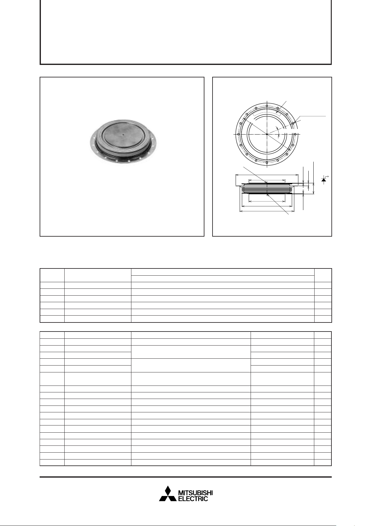
OUTLINE DRAWING Dimensions in mm
APPLICATION
Inverters, DC choppers, Induction heaters, DC to DC converters.
● ITQRM
Repetitive controllable on-state current
...........3000A
● I
T(AV) Average on-state current.....................1200A
● V
DRM
Repetitive peak off state voltage
...................4500V
● Anode short type
VRRM
VRSM
VR(DC)
VDRM
VDSM
VD(DC)
Unit
Symbol
Parameter
V
V
V
V
V
V
Voltage class
Repetitive peak reverse voltage
Non-repetitive peak reverse voltage
DC reverse voltage
Repetitive peak off-state voltage
+
Non-repetitive peak off-state voltage
+
DC off-state voltage
+
MAXIMUM RATINGS
3000
1880
1200
20
1.7 × 10
6
500
10
19
1000
4000
10
120
200
6300
–40 ~ +125
–40 ~ +150
39 ~ 55
1600
A
A
A
kA
A
2
s
A/µs
V
V
A
A
kW
kW
W
W
°C
°C
kN
g
V
DM = 3375V, CS = 3.0µF, LS = 0.4µH, Tj = 25/125°C
Applied for all conduction angles
f = 60Hz, sinewave θ = 180°, T
f = 78°C
One half cycle at 60Hz, T
j = 125°C
V
D = 2250V, ITM = 3000A, IGM= 100A, Tj= 125°C
di
G/dt = 50A/µs, CS = 3µF, RS = 5Ω
t
W = 20µs, f = 60Hz
t
W = 30µs, f = 60Hz
(Recommended value 47kN)
Typical value
Repetitive controllable on-state current
RMS on-state current
Average on-state current
Surge on-state current
Current-squared, time integration
Critical rate of rise of on-state current
Peak forward gate voltage
Peak reverse gate voltage
Peak forward gate current
Peak reverse gate current
Peak forward gate power dissipation
Peak reverse gate power dissipation
Average forward gate power dissipation
Average reverse gate power dissipation
Junction temperature
Storage temperature
Mounting force required
Weight
I
TQRM
IT(RMS)
IT(AV)
ITSM
I
2
t
diT/dt
VFGM
VRGM
IFGM
IRGM
PFGM
PRGM
PFG(AV)
PRG(AV)
Tj
Tstg
—
—
Symbol Parameter Conditions Ratings Unit
+ : VGK = –2V
NOTE1
φ3.5 ± 0.2 2.2 ± 0.2DEPTH
φ85 ± 0.2
+ 0
– 0.3
26 ± 0.5
φ120MAX
(φ127)
M3✕0.5 2.5DEPTH
0.4MIN
0.4MIN
(6.8)
φ134 ± 0.4
22.5° ± 0.5°
16-φ4.5
+0.2
0
φ147 ± 0.4
φ85 ± 0.2
(4 )

Aug.1998
On-state voltage
Repetitive peak reverse current
Repetitive peak off-state current
Reverse gate current
Critical rate of rise of off-state voltage
Delay time
Storage time
Peak gate turn-off current
Gate trigger current
Gate trigger voltage
Thermal resistance
3.5
100
150
100
—
3
3
—
4.0
1.5
0.01
—
—
—
—
—
—
—
—
—
—
—
—
—
—
—
1000
—
—
—
—
—
—
V
TM
IRRM
IDRM
IGRM
dv/dt
td
ts
IGQ
IGT
VGT
Rth(j-f)
V
mA
mA
mA
V/
µ
s
µ
s
µ
s
A
A
V
°C/W
I
T = 3000A, Tj = 125°C
V
RM = 19V, Tj = 125°C
V
DM = 4500V, VGK = –2V, Tj = 125°C
V
RG = 19V, Tj = 125°C
V
D = 2250V, Tj = 125°C, VGK = –2V (Expo. ware)
I
T = 3000A, VD = 2250V, IGM = 100A, Tj = 125°C
d
i/dt = 500A/µs, diG/dt = 50A/µs
C
S = 3µs, RS = 5Ω
MITSUBISHI GATE COMMUTATED TURN-OFF THYRISTORS
FG4000HX-90DS
HIGH POWER INVERTER USE
PRESS PACK TYPE
ELECTRICAL CHARACTERISTICS
Symbol
Parameter Test conditions
Limits
Min Typ Max
Unit
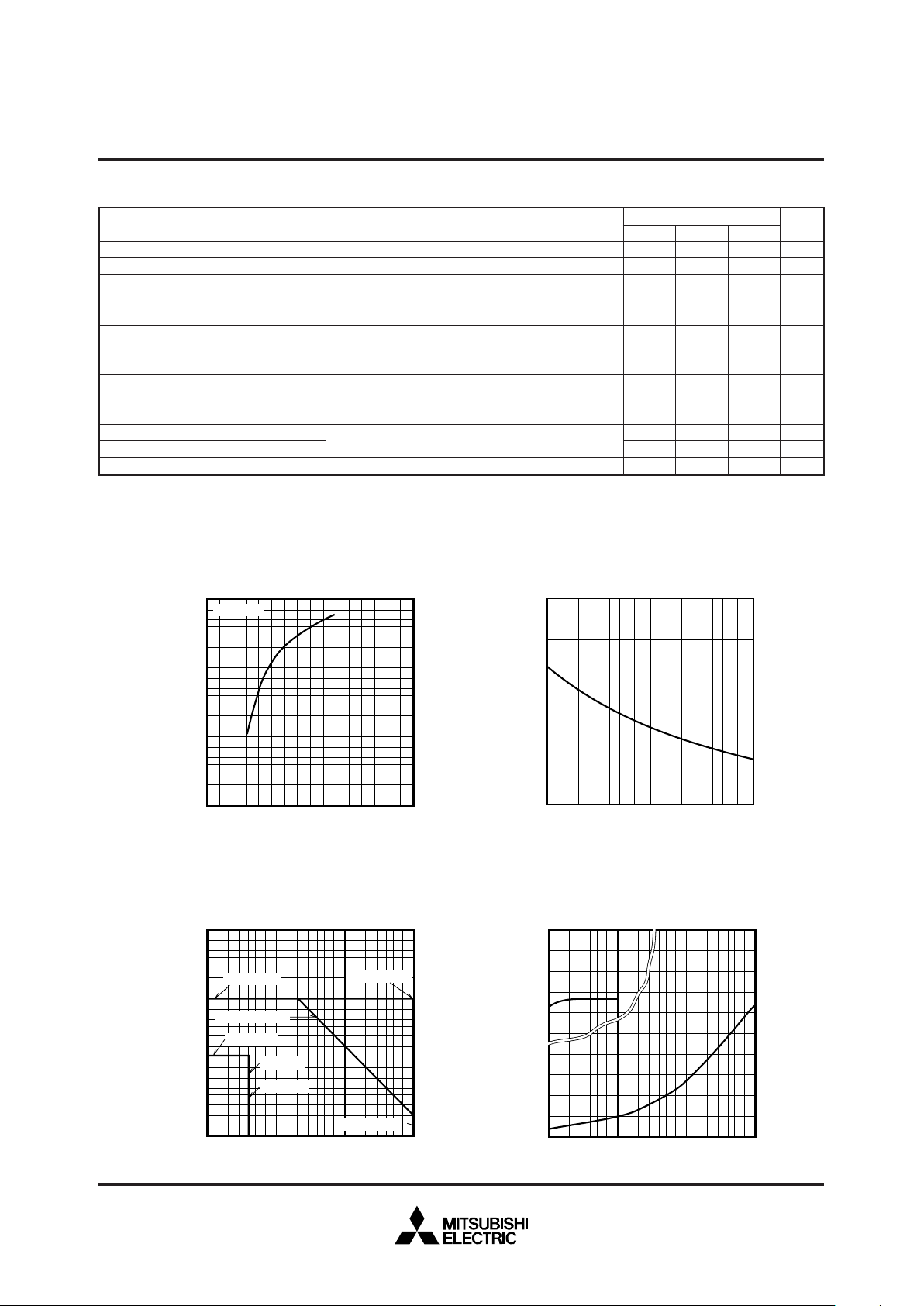
PERFORMANCE CURVES
MAXIMUM ON-STATE CHARACTERISTIC
ON-STATE CURRENT
(
A
)
ON-STATE VOLTAGE (V
)
RATED SURGE ON-STATE CURRENT
SURGE ON-STATE CURRENT (kA)
CONDUCTION TIME
(CYCLES AT 60Hz)
GATE CHARACTERISTICS
GATE VOLTAGE (V)
GATE CURRENT (mA)
MAXIMUM THERMAL IMPEDANCE
CHARACTERISTIC
(JUNCTION TO FIN)
THERMAL IMPEDANCE (°C/W)
TIME (S)
0 1.0 2.0 3.0 4.0 5.0 6.0 7.0 8.0
10
4
7
5
3
2
10
3
7
5
3
2
10
2
7
5
3
2
10
1
Tj = 125°C
30
24
21
18
12
3
0
9
6
15
27
10
0
23 57
10
1
23 57
10
2
10
0
23
10
0
57
10
1
23 57
10
2
23 57
10
3
10
2
7
5
3
2
10
1
7
5
3
2
7
5
3
2
10
–1
V
FGM
= 10V
VGT = 1.5V
P
FG(AV)
= 200W
I
FGM
= 1000A
Tj = 25°C
IGT = 4.0A
P
FGM
= 10kW
0.015
0
23
10
–3
57
10
–2
23
10
0
57
10
1
23 57
10
–1
23 57
10
0
0.006
0.009
0.012
0.003
IT = 3000A, VDM = 3375V, VD = 2250V
d
iGQ/dt = 6000A/µs, CS = 3.0µF, LS = 0.4µH
T
j = 125°C
Junction to fin
DC METHOD : V
D = 24V, RL = 0.1Ω, Tj = 25°C
 Loading...