

Page 1
2004
Service
Manual
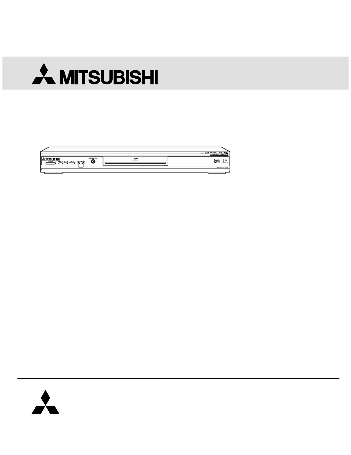
DVD PLAYER
MODEL
DD-8050
TABLE OF CONTENTS
SPECIFICATIONS . . . . . . . . . . . . . . . . . . . . . . . . . . . . . . . . . . . . . . . . . . . . . . . . . . . . . . . . . . . . . . . . . . . . . . .1-1-1
LASER BEAM SAFETY PRECAUTIONS. . . . . . . . . . . . . . . . . . . . . . . . . . . . . . . . . . . . . . . . . . . . . . . . . . . . . .1-2-1
IMPORTANT SAFETY PRECAUTIONS . . . . . . . . . . . . . . . . . . . . . . . . . . . . . . . . . . . . . . . . . . . . . . . . . . . . . .1-3-1
STANDARD NOTES FOR SERVICING. . . . . . . . . . . . . . . . . . . . . . . . . . . . . . . . . . . . . . . . . . . . . . . . . . . . . . .1-4-1
OPERATING CONTROLS AND FUNCTIONS. . . . . . . . . . . . . . . . . . . . . . . . . . . . . . . . . . . . . . . . . . . . . . . . . .1-5-1
CABINET DISASSEMBLY INSTRUCTIONS . . . . . . . . . . . . . . . . . . . . . . . . . . . . . . . . . . . . . . . . . . . . . . . . . . .1-6-1
BLOCK DIAGRAMS . . . . . . . . . . . . . . . . . . . . . . . . . . . . . . . . . . . . . . . . . . . . . . . . . . . . . . . . . . . . . . . . . . . . . .1-7-1
SCHEMATIC DIAGRAMS / CBA'S AND TEST POINTS . . . . . . . . . . . . . . . . . . . . . . . . . . . . . . . . . . . . . . . . . .1-8-1
WAVEFORMS . . . . . . . . . . . . . . . . . . . . . . . . . . . . . . . . . . . . . . . . . . . . . . . . . . . . . . . . . . . . . . . . . . . . . . . . . .1-9-1
WIRING DIAGRAM . . . . . . . . . . . . . . . . . . . . . . . . . . . . . . . . . . . . . . . . . . . . . . . . . . . . . . . . . . . . . . . . . . . . .1-10-1
FIRMWARE RENEWAL MODE . . . . . . . . . . . . . . . . . . . . . . . . . . . . . . . . . . . . . . . . . . . . . . . . . . . . . . . . . . . .1-11-1
SYSTEM CONTROL TIMING CHARTS . . . . . . . . . . . . . . . . . . . . . . . . . . . . . . . . . . . . . . . . . . . . . . . . . . . . . .1-12-1
IC PIN FUNCTION DESCRIPTIONS . . . . . . . . . . . . . . . . . . . . . . . . . . . . . . . . . . . . . . . . . . . . . . . . . . . . . . . .1-13-1
LEAD IDENTIFICATIONS . . . . . . . . . . . . . . . . . . . . . . . . . . . . . . . . . . . . . . . . . . . . . . . . . . . . . . . . . . . . . . . .1-14-1
EXPLODED VIEWS . . . . . . . . . . . . . . . . . . . . . . . . . . . . . . . . . . . . . . . . . . . . . . . . . . . . . . . . . . . . . . . . . . . . .1-15-1
MECHANICAL PARTS LIST . . . . . . . . . . . . . . . . . . . . . . . . . . . . . . . . . . . . . . . . . . . . . . . . . . . . . . . . . . . . . .1-16-1
ELECTRICAL PARTS LIST . . . . . . . . . . . . . . . . . . . . . . . . . . . . . . . . . . . . . . . . . . . . . . . . . . . . . . . . . . . . . . .1-17-1
MITSUBISHI ELECTRIC
MITSUBISHI DIGITAL ELECTRONICS AMERICA, INC.
9351 Jeronimo Road, Irvine, CA 92618-1904
Copyright © 2003 Mitsubishi Digital Electronics America, Inc.
All Rights Reserved
Page 2

Manufactured under license from Dolby Laboratories. "Dolby"
and the double-D symbol are trademarks of Dolby Laboratories.
Page 3

SPECIFICATIONS
ITEM CONDITIONS UNIT NOMINAL LIMIT
1. Video Output 75 ohm load Vpp 1.0 ± 0.1
2. Optical Digital Out dBm -18
3. Audio (PCM)
3-1. Output Level 1 kHz 0 dB Vrms 2.0
3-2. S/N dB 120
3-3. Freq. Response
DVD fs=48kHz ± 0.5dB Hz 20~22 k
CD fs=44.1kHz ± 0.5dB Hz 20~20 k
3-4. THD+N
DVD 1 kHz 0dB % 0.004
CD 1 kHz 0dB % 0.0045
NOTES:
1. All Items are measured without pre-emphasis unless otherwise specified.
2. Power supply : AC120 V 60 Hz
3. Load imp. : 100 k ohm
4. Ambient Temperature : +25
°C
1-1-1 E5932SP
Page 4
LASER BEAM SAFETY PRECAUTIONS
This DVD player uses a pickup that emits a laser beam.
Do not look directly at the laser beam coming
from the pickup or allow it to strike against your
skin.
The laser beam is emitted from the location shown in the figure. When checking the laser diode, be sure to keep
your eyes at least 30cm away from the pickup lens when the diode is turned on. Do not look directly at the laser
beam.
Caution: Use of controls and adjustments, or doing procedures other than those specified herein, may result in
hazardous radiation exposure.
Drive Mecha Assembly
Laser Beam Radiation
Laser Pickup
Turntable
WHEN OPEN. DO NOT
CAUTION
LASER RADIATION
STARE INTO BEAM.
Location: Top of DVD mechanism.
1-2-1 E5_LASER
Page 5

IMPORTANT SAFETY PRECAUTIONS
Product Safety Notice
Some electrical and mechanical parts have special
safety-related characteristics which are often not evident from visual inspection, nor can the protection they
give necessarily be obtained by replacing them with
components rated for higher voltage, wattage, etc.
Parts that have special safety characteristics are identified by a # on schematics and in parts lists. Use of a
substitute replacement that does not have the same
safety characteristics as the recommended replacement part might create shock, fire, and/or other hazards. The Product’s Safety is under review
continuously and new instructions are issued whenever appropriate. Prior to shipment from the factory,
our products are carefully inspected to confirm with
the recognized product safety and electrical codes of
the countries in which they are to be sold. However, in
order to maintain such compliance, it is equally important to implement the following precautions when a set
is being serviced.
Precautions during Servicing
A. Parts identified by the # symbol are critical for
safety. Replace only with part number specified.
B. In addition to safety, other parts and assemblies
are specified for conformance with regulations
applying to spurious radiation. These must also be
replaced only with specified replacements.
Examples: RF converters, RF cables, noise blocking capacitors, and noise blocking filters, etc.
C. Use specified internal wiring. Note especially:
1)Wires covered with PVC tubing
2)Double insulated wires
3)High voltage leads
D. Use specified insulating materials for hazardous
live parts. Note especially:
1)Insulation tape
2)PVC tubing
3)Spacers
4)Insulators for transistors
E. When replacing AC primary side components
(transformers, power cord, etc.), wrap ends of
wires securely about the terminals before soldering.
F. Observe that the wires do not contact heat produc-
ing parts (heatsinks, oxide metal film resistors, fusible resistors, etc.).
G. Check that replaced wires do not contact sharp
edges or pointed parts.
H. When a power cord has been replaced, check that
5 - 6 kg of force in any direction will not loosen it.
I. Also check areas surrounding repaired locations.
J. Be careful that foreign objects (screws, solder
droplets, etc.) do not remain inside the set.
K. Crimp type wire connector
The power transformer uses crimp type connectors
which connect the power cord and the primary side
of the transformer. When replacing the transformer,
follow these steps carefully and precisely to prevent
shock hazards.
Replacement procedure
1)Remove the old connector by cutting the wires at a
point close to the connector.
Important: Do not re-use a connector. (Discard it.)
2)Strip about 15 mm of the insulation from the ends
of the wires. If the wires are stranded, twist the
strands to avoid frayed conductors.
3)Align the lengths of the wires to be connected.
Insert the wires fully into the connector.
4)Use a crimping tool to crimp the metal sleeve at its
center. Be sure to crimp fully to the complete closure of the tool.
L. When connecting or disconnecting the internal
connectors, first, disconnect the AC plug from the
AC outlet.
1-3-1 DVD_SFN1
Page 6
Safety Check after Servicing
Examine the area surrounding the repaired location for
damage or deterioration. Observe that screws, parts,
and wires have been returned to their original positions. Afterwards, do the following tests and confirm
the specified values to verify compliance with safety
standards.
1. Clearance Distance
When replacing primary circuit components, confirm
specified clearance distance (d) and (d’) between soldered terminals, and between terminals and surrounding metallic parts. (See Fig. 1)
Table 1: Ratings for selected area
AC Line Voltage Clearance Distance (d), (d’)
Chassis or Secondary Conductor
Primary Circuit Terminals
dd'
120 V
Note: This table is unofficial and for reference only.
Be sure to confirm the precise values.
2. Leakage Current Test
Confirm the specified (or lower) leakage current
between B (earth ground, power cord plug prongs)
and externally exposed accessible parts (RF terminals, antenna terminals, video and audio input and
output terminals, microphone jacks, earphone jacks,
etc.) is lower than or equal to the specified value in the
table below.
Measuring Method (Power ON) :
Insert load Z between B (earth ground, power cord
plug prongs) and exposed accessible parts. Use an
AC voltmeter to measure across the terminals of load
Z. See Fig. 2 and the following table.
Table 2: Leakage current ratings for selected areas
AC Line Voltage Load Z Leakage Current (i) Earth Ground (B) to:
120 V
≥ 3.2mm (0.126 inches)
0.15µF CAP. & 1.5kΩ RES.
Connected in parallel
Exposed Accessible Part
Z
1.5k
i≤0.5mA Peak Exposed accessible parts
0.15 F
Earth Ground
B
Power Cord Plug Prongs
AC Voltmeter
(High Impedance)
Fig. 1
Fig. 2
Note: This table is unofficial and for reference only. Be sure to confirm the precise values.
1-3-2 DVD_SFN1
Page 7
STANDARD NOTES FOR SERVICING
Circuit Board Indications
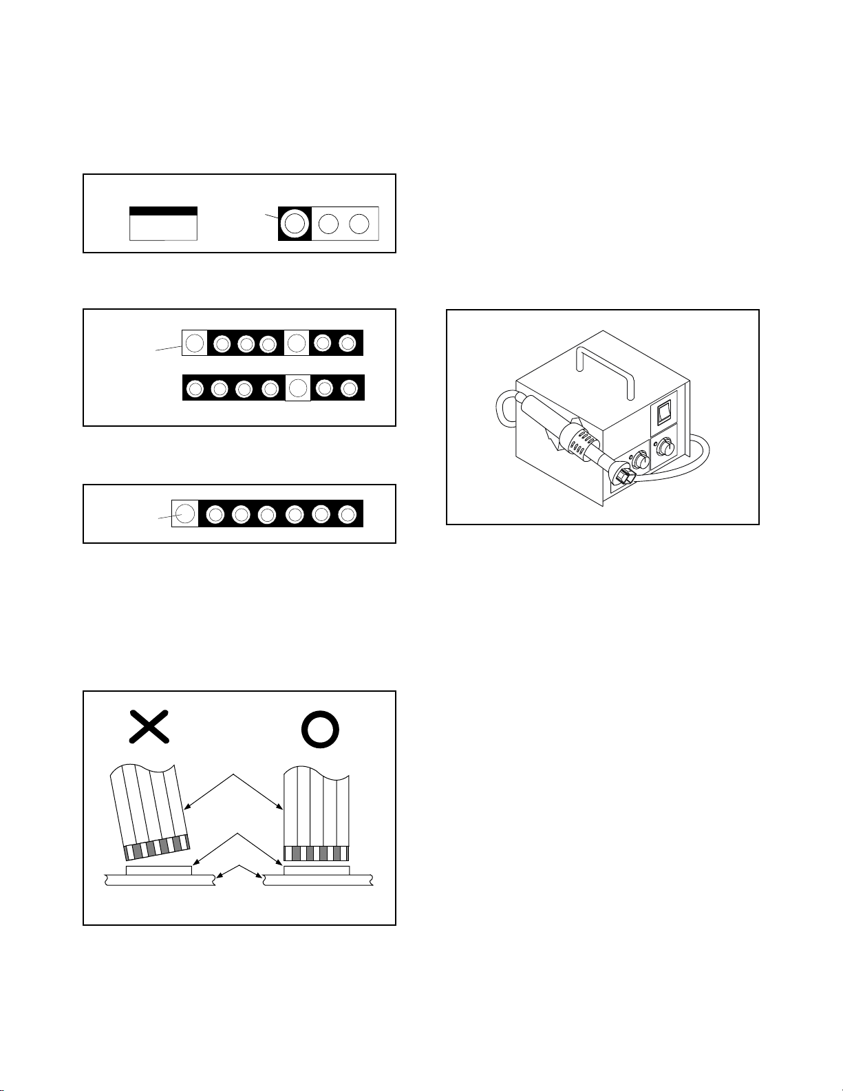
1. The output pin of the 3 pin Regulator ICs is indicated as shown.
Top View
Out
2. For other ICs, pin 1 and every fifth pin are indicated
as shown.
Pin 1
3. The 1st pin of every male connector is indicated as
shown.
Input
In
Bottom View
5
10
Pb (Lead) Free Solder
When soldering, be sure to use the Pb free solder.
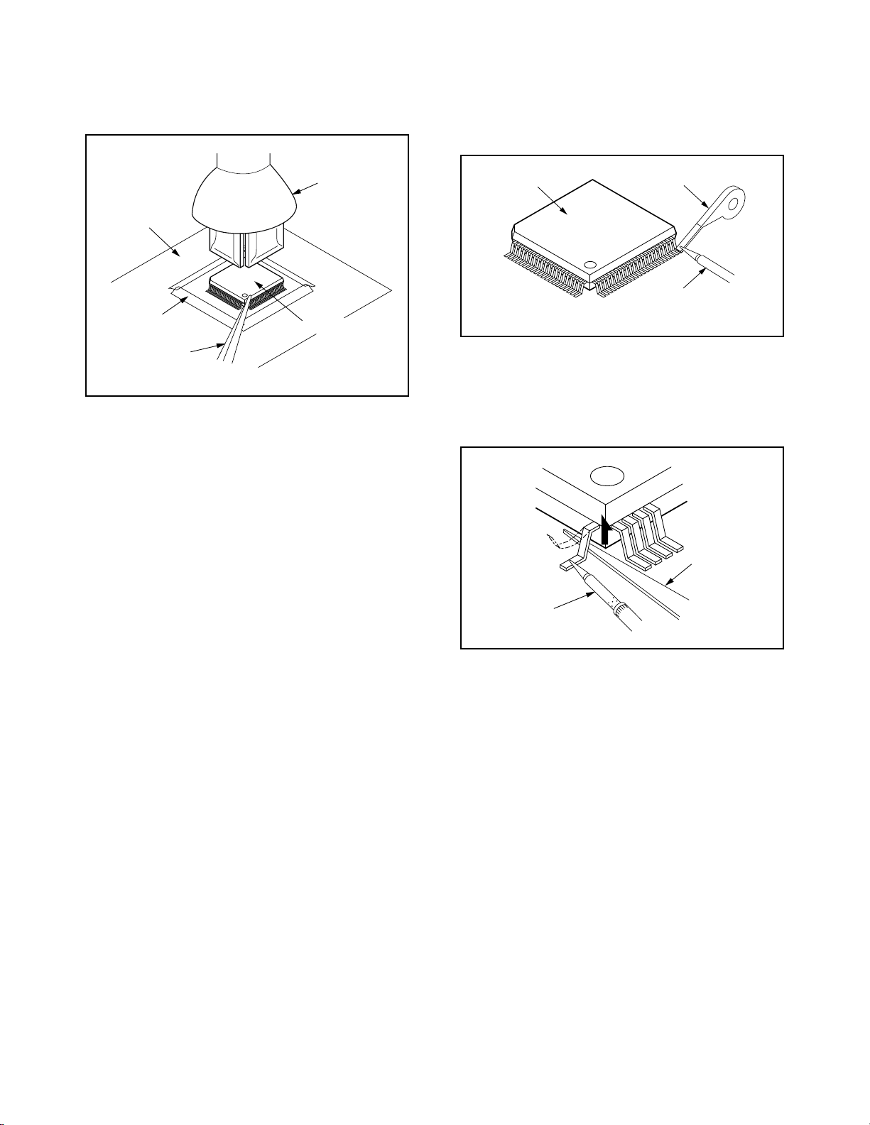
How to Remove / Install Flat Pack-IC
1. Removal
With Hot-Air Flat Pack-IC Desoldering Machine:.
(1) Prepare the hot-air flat pack-IC desoldering
machine, then apply hot air to the Flat Pack-IC
(about 5 to 6 seconds). (Fig. S-1-1)
Pin 1
Instructions for Connectors
1. When you connect or disconnect the FFC (Flexible
Foil Connector) cable, be sure to first disconnect
the AC cord.
2. FFC (Flexible Foil Connector) cable should be
inserted parallel into the connector, not at an angle.
FFC Cable
Connector
CBA
* Be careful to avoid a short circuit.
Fig. S-1-1
(2) Remove the flat pack-IC with tweezers while apply-
ing the hot air.
(3) Bottom of the flat pack-IC is fixed with glue to the
CBA; when removing entire flat pack-IC, first apply
soldering iron to center of the flat pack-IC and heat
up. Then remove (glue will be melted). (Fig. S-1-6)
(4) Release the flat pack-IC from the CBA using twee-
zers. (Fig. S-1-6)
Caution:
1. The Flat Pack-IC shape may differ by models. Use
an appropriate hot-air flat pack-IC desoldering
machine, whose shape matches that of the Flat
Pack-IC.
2. Do not supply hot air to the chip parts around the
flat pack-IC for over 6 seconds because damage to
the chip parts may occur. Put masking tape around
the flat pack-IC to protect other parts from damage.
(Fig. S-1-2)
1-4-1 E5STA
Page 8
3. The flat pack-IC on the CBA is affixed with glue, so
be careful not to break or damage the foil of each
pin or the solder lands under the IC when removing
it.
With Soldering Iron:
(1) Using desoldering braid, remove the solder from all
pins of the flat pack-IC. When you use solder flux
which is applied to all pins of the flat pack-IC, you
can remove it easily. (Fig. S-1-3)
CBA
Masking
Tape
Tweezers
Hot-air
Flat Pack-IC
Desoldering
Machine
Flat Pack-IC
Fig. S-1-2
Flat Pack-IC
Desoldering Braid
Soldering Iron
Fig. S-1-3
(2) Lift each lead of the flat pack-IC upward one by
one, using a sharp pin or wire to which solder will
not adhere (iron wire). When heating the pins, use
a fine tip soldering iron or a hot air desoldering
machine. (Fig. S-1-4)
Sharp
Pin
Fine Tip
Soldering Iron
(3) Bottom of the flat pack-IC is fixed with glue to the
CBA; when removing entire flat pack-IC, first apply
soldering iron to center of the flat pack-IC and heat
up. Then remove (glue will be melted). (Fig. S-1-6)
(4) Release the flat pack-IC from the CBA using twee-
zers. (Fig. S-1-6)
Fig. S-1-4
1-4-2 E5STA
Page 9
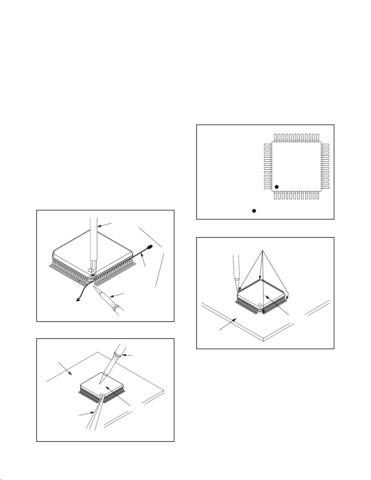
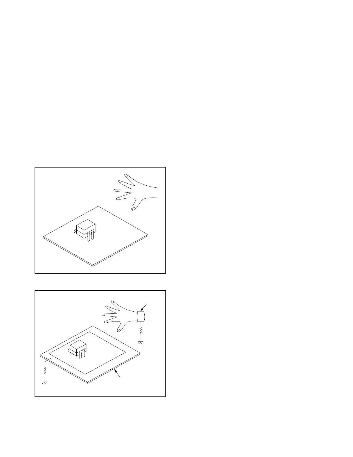
With Iron Wire:
(1) Using desoldering braid, remove the solder from all
pins of the flat pack-IC. When you use solder flux
which is applied to all pins of the flat pack-IC, you
can remove it easily. (Fig. S-1-3)
(2) Affix the wire to a workbench or solid mounting
point, as shown in Fig. S-1-5.
(3) While heating the pins using a fine tip soldering
iron or hot air blower, pull up the wire as the solder
melts so as to lift the IC leads from the CBA contact
pads as shown in Fig. S-1-5.
(4) Bottom of the flat pack-IC is fixed with glue to the
CBA; when removing entire flat pack-IC, first apply
soldering iron to center of the flat pack-IC and heat
up. Then remove (glue will be melted). (Fig. S-1-6)
(5) Release the flat pack-IC from the CBA using twee-
zers. (Fig. S-1-6)
Note:
When using a soldering iron, care must be taken
to ensure that the flat pack-IC is not being held by
glue. When the flat pack-IC is removed from the
CBA, handle it gently because it may be damaged
if force is applied.
Hot Air Blower
2. Installation
(1) Using desoldering braid, remove the solder from
the foil of each pin of the flat pack-IC on the CBA so
you can install a replacement flat pack-IC more
easily.
(2) The “I” mark on the flat pack-IC indicates pin 1.
(See Fig. S-1-7.) Be sure this mark matches the 1
on the PCB when positioning for installation. Then
presolder the four corners of the flat pack-IC. (See
Fig. S-1-8.)
(3) Solder all pins of the flat pack-IC. Be sure that none
of the pins have solder bridges.
Example :
Pin 1 of the Flat Pack-IC
is indicated by a " " mark.
Fig. S-1-7
To Solid
Mounting Point
CBA
Tweezers
Iron Wire
Soldering Iron
Fig. S-1-5
Fine Tip
Soldering Iron
Flat Pack-IC
or
Presolder
Flat Pack-IC
CBA
Fig. S-1-8
Fig. S-1-6
1-4-3 E5STA
Page 10
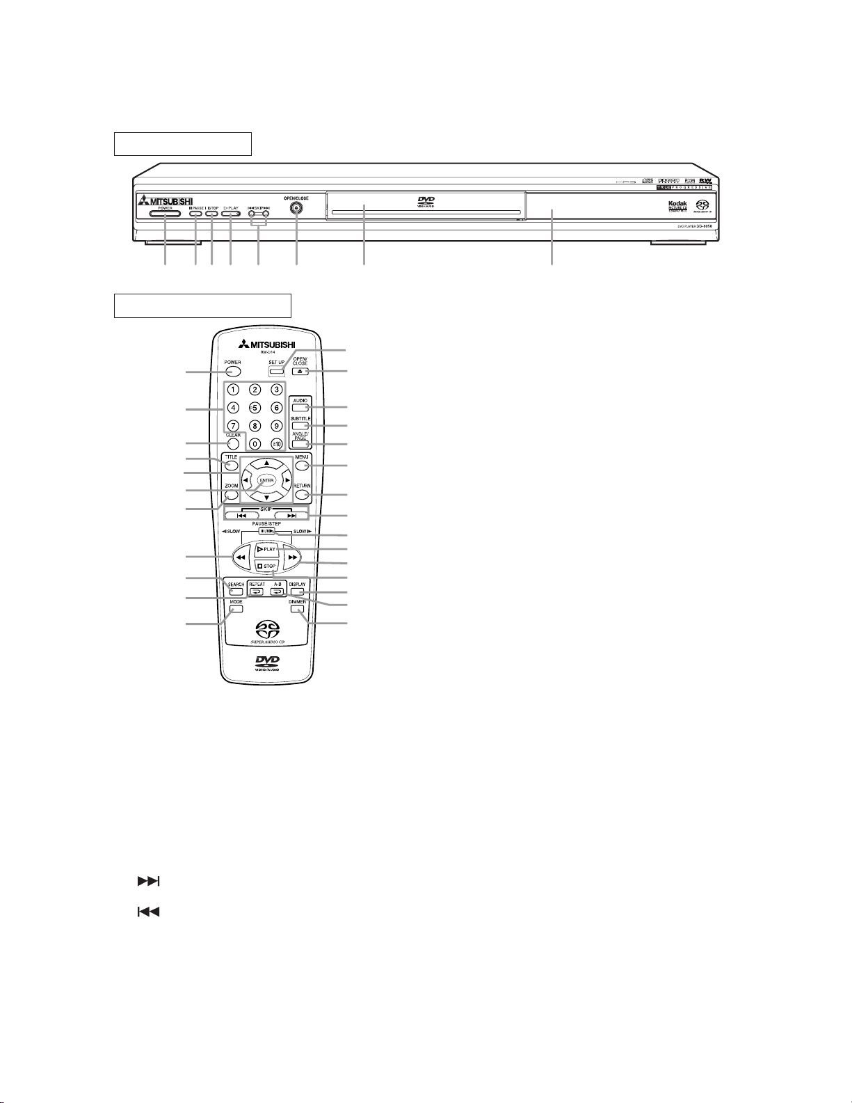
Instructions for Handling
Semi-conductors
Electrostatic breakdown of the semi-conductors may
occur due to a potential difference caused by electrostatic charge during unpacking or repair work.
1. Ground for Human Body
Be sure to wear a grounding band (1MΩ) that is properly grounded to remove any static electricity that may
be charged on the body.
2. Ground for Workbench
(1) Be sure to place a conductive sheet or copper plate
with proper grounding (1MΩ) on the workbench or
other surface, where the semi-conductors are to be
placed. Because the static electricity charge on
clothing will not escape through the body grounding band, be careful to avoid contacting semi-conductors with your clothing.
<Incorrect>
<Correct>
1MΩ
CBA
Grounding Band
1MΩ
CBA
Conductive Sheet or
Copper Plate
1-4-4 E5STA
Page 11
OPERATING CONTROLS AND FUNCTIONS
us
or
de
or
ty
ol.
V
ce
e.
s.
FRONT PANEL
4 5 6 7 8321
®
REMOTE CONTROL
28
1
9
10
11
12
13
14
15
16
17
18
1. POWER Button
Press to turn the power on and off.
2. PAUSE Button (main unit)
Pauses the current disc operation.
PAUSE/STEP Button (remote control)
Pauses the current disc operation. View the still
picture frame by frame.
3. STOP Button
Stops operation of the disc.
4. PLAY Button
Starts playback of the disc contents.
5. SKIP Buttons
: Plays back from the beginning of the next
chapter or track.
: Plays back from the beginning of the current
chapter or track.
6. OPEN/CLOSE Button
Press to insert or remove discs from the tray.
7. Disc loading tray
8. Display, Remote Sensor Window
6
27
26
25
24
23
5
2
4
22
3
21
20
19
9. Numeric Buttons
10. CLEAR Button
Resets a setting.
11. TITLE Button
Displays the title menu.
12. Arrow Buttons
Use to scroll and cycle through disc and player men
and settings.
13. ENTER Button
Press to accept a setting.
14. ZOOM Button
Enlarges part of a DVD-reproduced image.
15. REV Button
Fast reverse playback to a desired point.
16. SEARCH MODE Button
Press to locate a desired point.
17. REPEAT Button
Repeats playback of the current disc, title, chapter
track.
18. MODE Button
Activates program playback or random playback mo
when playing DVD-Audio, CDs, Super Audio CDs
MP3/JPEG/Picture CD/WMA. Also Sets Image Quali
setting, Black Level, Virtual Surround and Speech Contr
19. DIMMER Button
Select the display panel brightness.
20. A-B REPEAT Button
Repeats playback of a selected section.
21. DISPLAY Button
Displays timer and bit-rate information on the T
screen.
22. FWD Button
Fast forwards playback to a desired point.
23. RETURN Button
Returns to the previous operation.
24. MENU Button
Displays the disc menus.
25. ANGLE/PAGE Buttons
Press to change the camera angle to see the sequen
being played back from a different angle.
Press to select the image to be displayed.
26. SUBTITLE Button
Press to select a desired subtitle language.
27. AUDIO Button
Press to select a desired audio language or sound mod
28. SETUP Button
Press to enter the setup mode or to change setup item
1-5-1 E5932IB
Page 12
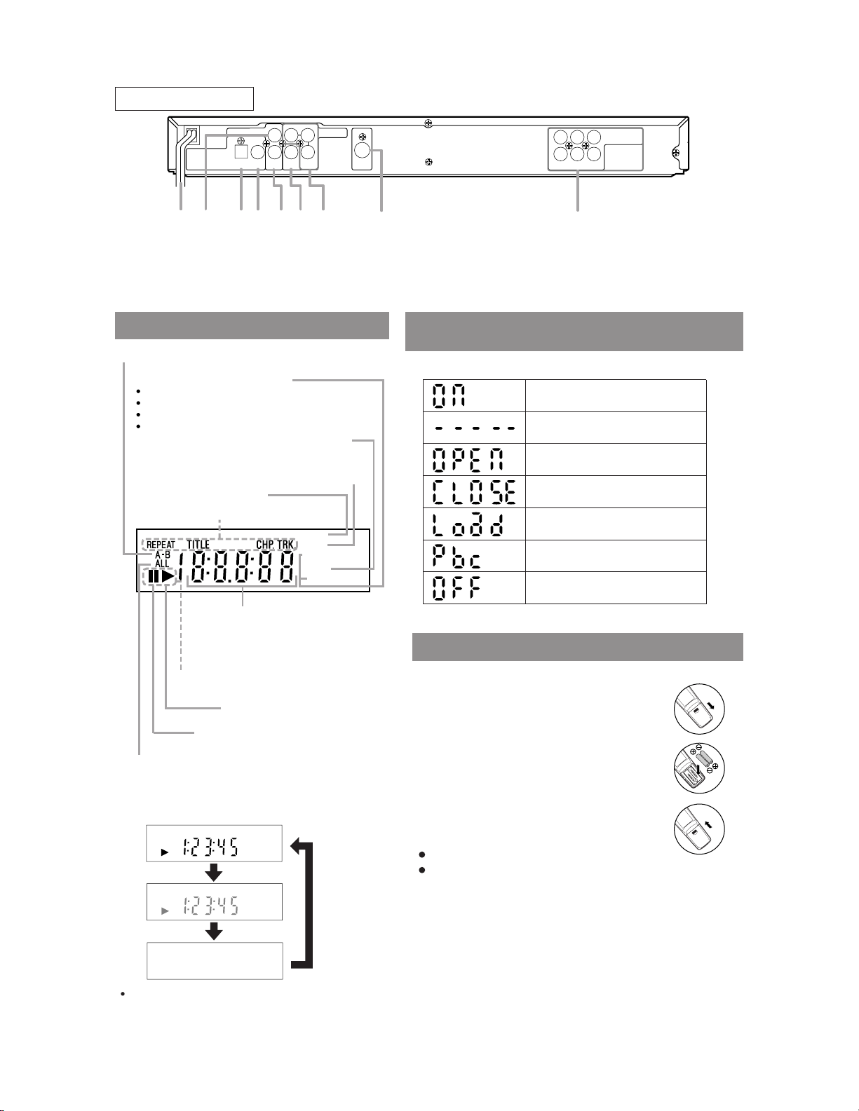
REAR VIEW
2
3
3
3
3
GROUP
SACD
P.SCAN
DVD A
VCD
M
Lights up when the A-B repeat function is on.
Lights up when the repeat function is on.
Lights up when
Progressive Scan is on.
Lights up when
playing a Super Audio CD.
Lights up when the ALL repeat function is on.
Lights up when the inserted
disc comes to a pause.
Lights up when playing MULTI-CH AREA
on Super Audio CD.
Displays a type of the disc
which is inserted on the tray.
: DVD disc
DVD
: DVD-audio
: VCD
:
Audio CD, MP3, JPEG, PictureCD, WMA
Lights up when the inserted
disc is being played back.
Lights up when the playback is
slow mode.
Displays how long the current
title or track has been played back.
When a chapter or track is
switched, the number of a new
title, chapter or track is displayed.
Power on
No disc inserted or playing DVD menu
Opening the Tray
Closing the Tray
Loading the disc
Lights up when the playback control is
activated (VCD)
Power off
Dark
OFF
Bright
DVD
DVD
LYCr
R
DIGITAL AUDIO OUT
(PCM/BITSTREAM)
AUDIO OUT
OPTICAL COAXIAL
29 34 36353330 3132 37
9. Power Cord
0. Left AUDIO OUT Jack
1. OPTICAL DIGITAL AUDIO OUT Jack
2. COAXIAL DIGITAL AUDIO OUT Jack
3. Right AUDIO OUT Jack
VIDEO
VIDEO OUT
Cb
S-VIDEO
ANALOG
L
R
SURROUND
SUBWOOFER
CENTER
5.1 CH
AUDIO OUT
L
R
OUT
FRONT
34. VIDEO OUT Jack
35. COMPONENT VIDEO OUT Jacks
36. S-VIDEO OUT Jack
37. ANALOG 5.1 CH AUDIO OUT Jacks
DISPLAY
DVD
VCD
CD
It is possible to change the brightness of display unit
by pressing the DIMMER button of remote control
When
the display is returned to the setup status.
the power supply is turned off,
DISPLAYS DURING
OPERATION
LOADING THE BATTERIES
1. Open the battery compartment cover.
2. Insert two AA batteries, with each one
oriented correctly.
3. Close the cover.
.
Notes
Do not mix alkaline and manganese batteries.
Do not mix old and new batteries.
1-5-2 E5932IB
Page 13
CABINET DISASSEMBLY INSTRUCTIONS
1. Disassembly Flowchart
This flowchart indicates the disassembly steps to gain
access to item(s) to be serviced. When reassembling,
follow the steps in reverse order. Bend, route, and
dress the cables as they were originally.
[6] Function
CBA
[2] Front
Assembly
[3] Reinforce
Plate
[8] DVD
Mecha
[9] Main
PCB Holder
[10] 5.1ch
Amp CBA
[1] Top Case
[4] DVD Main
CBA Unit
[11] Jack
PCB Holder
[5] Rear
Panel
[7] AV CBA
2. Disassembly Method
ID/
LOC.
No.
[1] Top Case D1 5(S-1) ---
[2]
[3]
[4]
[5] Rear Panel D4 7(S-4), (S-5) ---
[6]
[7] AV CBA D5 (S-6), (S-7), *CN1301 ---
[8]
[9]
[10]
[11]
PAR T
Front
Assembly
Reinforce
Plate
DVD Main
CBA Unit
Function
CBA
DVD
Mecha
Main PCB
Holder
5.1ch Amp
CBA
Jack PCB
Holder
Fig.
No.
D2
D2 2(S-2) ---
D3
D5 *CN2001 ---
D6 4(S-8) ---
D6 2(S-9) ---
D6 *2(L-4) ---
D6 2(S-10) ---
REMOVAL
REMOVE/*UNHOOK/
UNLOCK/RELEASE/
UNPLUG/DESOLDER
*4(L-1), *3(L-2),
*3(L-3)
(S-3A), 2(S-3B),
*CN201, *CN301,
*CN401, *CN501,
*CN601
Note
1
1-1
1-2
2
2-1
2-1
3
(1): Identification (location) No. of parts in the figures
(2): Name of the part
(3): Figure Number for reference
(4): Identification of parts to be removed, unhooked,
unlocked, released, unplugged, unclamped, or
desoldered.
P=Spring, L=Locking Tab, S=Screw,
CN=Connector
*=Unhook, Unlock, Release, Unplug, or Desolder
e.g. 2(S-2) = two Screws (S-2),
2(L-2) = two Locking Tabs (L-2)
(5): Refer to “Reference Notes.”
About tightening screws
When tightening screws, tighten them with the following torque.
Screws Torque
(S-1), (S-2), (S-3A),
(S-4), (S-5), (S-6),
(S-7), (S-8), (S-9),
(S-10)
(S-3B) 0.38 ± 0.04 N·m
0.45 ± 0.05 N·m
Reference Notes
CAUTION 1: Locking Tabs (L-1), (L-2) and (L-3) are
fragile. Be careful not to break them.
1-1. Release four Locking Tabs (L-1) and three Lock-
ing Tabs (L-2).
1-2. Release three Locking Tabs (L-3), then remove
the Front Assembly.
CAUTION 2: Electrostatic breakdown of the laser
diode in the optical system block may occur as a
potential difference caused by electrostatic charge
accumulated on cloth, human body etc, during
unpacking or repair work.
To avoid damage of pickup follow next procedures.
2-1. Short the three short lands of FPC cable with sol-
der before removing the FFC cable (CN201) from
it. If you disconnect the FFC cable (CN201), the
laser diode of pickup will be destroyed. (Fig. D4)
2-2. Remove Screw (S-3A) and two Screws (S-3B).
Then disconnect Connectors (CN301), (CN401),
(CN501) and (CN601) and lift the DVD Main CBA
Unit. (Fig. D3)
CAUTION 3: When reassembling, confirm the FFC
cable (CN201) is connected completely. Then remove
the solder from the three short lands of FPC cable.
(Fig. D3)
↓
(1)
↓
(2)
↓
(3)
↓
(4)
↓
(5)
1-6-1 E5932DC
Page 14
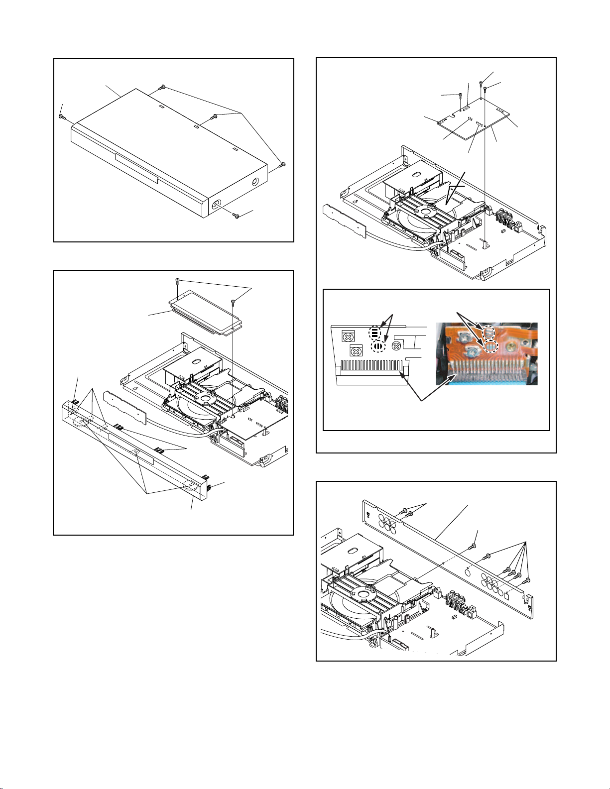
[1] Top Case
(S-1)
[3] Reinforce Plate
(S-1)
(S-1)
Fig. D1
(S-2)
CN201
(S-3B)
CN501
CN301
CN401
(S-3B)
(S-3A)
[4] DVD Main
CBA Unit
A
Short the three short lands by soldering.
(Either of two places.)
CN601
(L-1)
(L-3)
(L-1)
(L-2)
[2] Front Assembly
(L-1)
Fig. D2
Connector
View for A
(S-4)
Fig. D3
[5] Rear Panel
(S-5)
(S-4)
Fig. D4
1-6-2 E5932DC
Page 15
[6] Function CBA
(S-6)
CN2001
CN1301
(S-7)
[7] AV CBA
[10] 5.1ch Amp CBA
(S-10)
[11] Jack
PCB
Holder
(S-8)
(S-8)
(L-4)
Fig. D5
HOW TO EJECT MANUALLY (Method 1)
1. Remove the Top Case, Reinforce Plate and DVD Main CBA Unit.
2. Rotate the roulette in the direction of the arrow as shown below.
(L-4)
View for A
[8] DVD
Mecha
(S-9)
[9] Main
PCB
Holder
Fig. D6
Rotate this roulette in
the direction of the arrow
A
1-6-3 E5932DC
Page 16

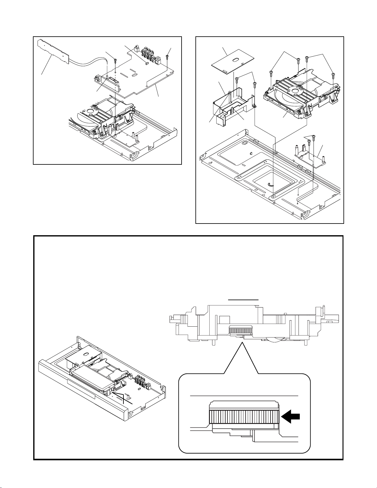
HOW TO EJECT MANUALLY (Method 2)
1. Turn the unit over.
2. Insert the shaft less than a diameter of 3 mm (e.g. screwdriver) straightly into the opening as shown.
3. Turn the shaft along with the opening clockwise.
4. Repeat steps 2 and 3 until the tray will open.
5. Pull the tray slowly with a hand.
View for B
Rear
Turn the shaft along with
the opening clockwise.
Shaft
(e.g. screwdriver)
Opening
B
Front
1-6-4 E5932DC
Page 17

BLOCK DIAGRAMS
System Control / Servo Block Diagram
FL2001
GRID FIP
~
23
17
~
7G
1G
IC2001
(FRONT PANEL CONTROL)
789
a/KEY-1
b/KEY-2
SEGMENT
10
c/KEY-3
d/KEY-4
12
11
f
e
FP-STB
2
CN1001
131416
g
h
FP-DIN
FP-DOUT
28
27
KEY-1 5
5
CN2001 CN2101
i
FP-CLK
1
KEY
MATRIX
FUNCTION CBA
KEY-3 4
K2 1
KEY-2 3
KEY-4 6
K1 2
4
1
3
6
2
3
4
K1
K2
AV CBA
SENSOR
REMOTE
RM2001
IC101
(MICRO CONTROLLER)
DVD MAIN CBA UNIT
A-MUTE
53
77 M-MUTE
ADAC-MD
57
56 ADAC-MC
86 ADAC-ML
IC462
+3.3V
IC461
+3.3V
RESET73
RESET
1 3
RESET
2 1
VREF
(SERVO DRIVE)
IC301
FOCUS DRIVE
FD-OFST
148
146
25
27
26
-
+
-
+
FOCUS
ACTUATOR
DRIVE
15
16
24
TRACKING
DRIVE
TD-OFST
147
139
-
+
-
+
TRACKING
ACTUATOR
DRIVE
14
13
312
SPDL
76
-
+
-
+
SPINDLE
MOTOR
DRIVE
12
11
645
FP-STB 20
FP-DIN 19
2221232024
CN401
82
60
FP-DIN
FP-STB
SLD
75
23
-
+
SLED
MOTOR
DRIVE
17
18
FP-DOUT 21
FP-CLK 18
REMOTE 22
61
67
59
FP-CLK
REMOTE
FP-DOUT
IC202
(OP AMP)
10
1FG-IN
TRAY-IN
66
8
9
3SP(+)
675
+3.3V
4SP(-)
5TRAY-IN
SL-AMP72FG-IN
81
14
13
12
6GND
7SL(-)
8SL(+)
SP-ROT
143
1
2
3
CN301
ADAC-MD
TO SACD
ADAC-MC
BLOCK DIAGRAM
M-MUTE
A-MUTE
TO AUDIO
ADAC-MD
BLOCK DIAGRAM
ADAC-MC
ADAC-ML
FS(+)
FS(-)
TO DIGITAL SIGNAL
TS(+)
TS(-)
PROCESS BLOCK
DIAGRAM
1-7-1
DRIVE CBA
TRAY-IN
SPINDLE
MOTOR
M
SLED
MOTOR
M
FG
SENSOR
FG CBA
E5932BLS
Page 18

Digital Signal Process Block Diagram
TO SACD
BLOCK
DATA(AUDIO) SIGNAL
DATA(VIDEO/AUDIO) SIGNAL VIDEO SIGNAL
SD1
SD2
SD0/SPDIF
177
176
175
SD3
174
DATA
SD4
171
RAM
SD5
SD6
170
INST.
DSP
DECODER
169
ROM
SD7
163
XSHD
187
XSHD
DATA
DIAGRAM
XSAK
186
XSAK
RAM
I/O
SDCK
RESET
185
189
SDCK
RESET
INST.
PROCESSOR
XSRQ
ROM
SDEF
168
XSRQ
PSP-WCK
SACD-READY
88
188
SDEF
PSP-WCK
SACD-DATA
SACD-LATCH
55
58
SACD-DATA
SACD-READY
SD0/SPDIF
54
SACD-LATCH
AUDIO
SD1
I/F
TO AUDIO
SD2
SD3
SERIAL
BLOCK
DIAGRAM
SD4
SD5
GENERAL
I/O
CPU
SD6
I/F
INTERRUPT
SACD
68
SACD
CONTROLLER
TIMER
VIDEO-C
VIDEO-Y(I)
156
C
Y(I)
D/A
WATCH DOG
TIMER
TO VIDEO
VIDEO-Cr/Pr
158
Cr/Pr
D/A
NTSC/PAL
VIDEO
REMOTE
CONTROL
BLOCK
DIAGRAM
VIDEO-Cb/Pb
152
Cb/Pb
D/A
ENCODER
I/F
VIDEO-Y
151
Y
D/A
32BIT CPU
BCU
149
D/A
DATA
INST
DEBUG
RAM
RAM
IC103 (FLASH ROM)
~
~
293638
45
EXADT (0-15)
ICS13(LATCH)
EXADT (0-15), EADR (16-19)
FLASH
ROM
EADR (0-7)
~
12
19
D TYPE
LATCH
~
2
9
EXADT (0-7)
~
1
9
162548
EADR (16-19)
ICS14(LATCH)
~
EADR (0-15)
EADR (8-15)
~
12
19
D TYPE
LATCH
~
2
9
EXADT (8-15)
SDRAM ADDRESS(0-11)
IC101 (MICRO CONTROLLER)
~
217
SDRAM ADDRESS(0-11)
~~
212760
ICS04 (SDRAM)
EXTERNAL
MEMORY
I/F
1
238
~~~
2
13314245567485
66
SDRAM
STREAM
I/F
DECODER
I/F
ECC
SDRAM DATA(0-15)
~~~
18
192
212
SDRAM DATA(0-31)
252
256
UMAC
DMA
DVD/CD
FORMATTER
RF
SIGNAL
PROCESS
CIRCUIT
114
115
116
117
132
131
134
133
~
CN201
C16
A17
B15
D18
DETECTOR
BCU
129
E14
130
F12
CD/DVD 19
READ
MEMORY
32BIT
INST.
ROM
126
AMP
Q253,Q254
CN201
CD-LD 10
CPU
DATA
RAM
124
125
Q251,Q252
AMP
DVD-LD 8
PD-MONI 7
123
6
5
9
GND(LD)
GND(CD-PD)
GND(DVD-PD)
CPU
I/F
WATCH DOG
TIMER
TIMER
INTERRUPT
CONTROLLER
CD/DVD
83
6
1 3
CD DVD
EXADT (0-15), EADR (16-19)
FSEL
27MHz
CLOCK
IC201
(SW)
4
69
166 165
+3.3V
FS
TS
(AND GATE)
ICS06
FS(+)
CN201
FS(+) 2
4
1
2
27MHz
OSC
X101
TO SYSTEM
CONTROL/SERVO
BLOCK DIAGRAM
FS(-)
TS(-)
TS(+)
FS(-) 3
TS(+) 1
TO SACD
BLOCK
DIAGRAM
CLK33M
9
14
CLK
GENE.
(CLOCK GENERATOR)
X'TAL
OSC
ICS03
7
DVD MAIN CBA UNIT
TS(-) 4
PICK-UP
UNIT
1-7-2
E5932BLD
Page 19

Video Block Diagram
VIDEO SIGNAL
JK1401
S-VIDEO OUT
2
1
3 4
YC
WF3
5
6
7
DRIVER
DRIVER
2dB
AMP
2dB
AMP
2dB
AMP
LPF DRIVER
4dB
AMP
IC1403 (VIDEO DRIVER)
3
4dB
LPF
AMP
1
COMPOSITE
VIDEO OUT
JK1404
2dB
4dB
IC1402 (VIDEO DRIVER)
VIDEO-Y
OUT
13
AMP
LPF DRIVER
AMP
3
VIDEO-Cb/Pb
OUT
11
2dB
AMP
2dB
LPF DRIVER
4dB
AMP
4dB
6
VIDEO-Cr/Pr
OUT
10
AMP
LPF DRIVER
AMP
8
88VIDEO-Y
33VIDEO-Y(I)
10 10VIDEO-C
VIDEO-Y
VIDEO-C
VIDEO-Cb/Pb
WF1
66VIDEO-Cb/Pb
44VIDEO-Cr/Pr
VIDEO-Cr/Pr
WF2
CN601 CN1601
VIDEO-Y(I)
DVD MAIN CBA UNIT AV CBA
TO DIGITAL
SIGNAL PROCESS
BLOCK DIAGRAM
1-7-3
E5932BLV
Page 20

Audio Block Diagram
FRONT-L
OUT
FRONT-R
OUT
AUDIO SIGNALDATA(AUDIO) SIGNAL
JK7101
MUTE-ON
MUTE-ON
Q7504
Q7503
1
(AMP)
IC7301
7
2
6
5.1CH AMP CBA
Q7552
Q7501
Q7502
Q7551
(AMP)
IC7401
SURROUND-L
OUT
Q7404
1
2
MUTE-ON
SURROUND-R
OUT
Q7403
7
6
MUTE-ON
Q7402
Q7452
Q7401
Q7451
(AMP)
IC7501
CENTER
OUT
Q7308
1
2
MUTE-ON
SUB
7
6
WOOFER
OUT
MUTE-ON
Q7307
Q7302
Q7352
Q7301
Q7351
IC1204
AV CBA
DIGITAL
OPTICAL
AUDIO
JK1202
Q1351
OUT
BUFFER
COAXIAL
(AMP)
IC1201
JK1404
1
2
AUDIO-L
OUT
Q1201
MUTE-ON
AUDIO-R
Q1202
7
6
OUT
MUTE-ON
Q1204
15
FRONT-AUDIO-L
15
CNS01 CN7102
13 13FRONT-AUDIO-R
99SURROUND-R
11 11SURROUND-L
77CENTER
55SUB WOOFER
14
A-L-MUTE
12 12A-R-MUTE
14
88SURROUND-R-MUTE
66CENTER-MUTE
44SUB WOOFER-MUTE
10 10SURROUND-L-MUTE
33A-MUTE
16 16A-MUTE2
22M-MUTE
WF4
WF6
CN601 CN1601
9
10
L-CH
R-CH
LPF+AMP
LPF+AMP
DAC
DAC
DSD
FILTER
ICS02 (AUDIO DAC)
DSD
373839404142434445
(X8 DF)
I/F
29
L-CH
LPF+AMP
DAC
28
R-CH
LPF+AMP
DAC
ENHANCED
MULTI-LEVEL
DELTA-SIGMA
31
L-CH
LPF+AMP
DAC
MODULATOR
30
R-CH
LPF+AMP
DAC
12
L-CH
LPF+AMP
DAC
PCM
FILTER
(X8 DF)
I/F
PCM
5150494847
11
R-CH
LPF+AMP
DAC
46
CONTROL
FUNCTION
2
3
4
19
SPDIF
19
16
AUDIO-R
14 14AUDIO-L
16
SYSTEM
13 13A-MUTE
8
A-MUTE2
CLOCK
33
WF5
15 15A-R-MUTE
7
A-R-MUTE
RESET
36
DVD MAIN CBA UNIT
A-L-MUTE
A-R-MUTE
SURROUND-L-MUTE
SURROUND-R-MUTE
TO SACD
BLOCK DIAGRAM
CENTER-MUTE
SUB WOOFER-MUTE
A-MUTE
M-MUTE
TO SYSTEM
CONTROL/SERVO
BLOCK DIAGRAM
DSD-CLK
DSD-MXL
DSD-MXR
DSD-FL
DSD-FR
DSD-C
DSD-SW
DSD-LS
TO SACD
BLOCK DIAGRAM
1-7-4
DSD-RS
(AND GATE)
ICS10
SD6
SD3
SD1
(AND GATE)
ICS07
SD4
SD0/SPDIF
4
2
1
SACD
(AND GATE)
ICS21
ADAC-MD
ADAC-MC
ADAC-ML
TO SYSTEM
CONTROL/SERVO
BLOCK DIAGRAM
4
1
2
CLK33M/36M
RESET
TO SACD
BLOCK DIAGRAM
4
4
(AND GATE)
ICS11
1
2
1
2
SD5
SD2
TO DIGITAL
SIGNAL PROCESS
BLOCK DIAGRAM
E5932BLA
Page 21

SACD Block Diagram
DATA(AUDIO) SIGNAL
ICS01 (SACD MULTI CHANNEL SIGNAL PROCESS)
ADAC-MD
4
ADAC-MC
3
XSRQ
TEST RESET
RESET
9
31
164
SDEF
168
WCK
123
TO AUDIO
TO AUDIO
DSD-CLK
DSD-XML
60
55
DSD-FL
DSD-FR
DSD-XMR
6466697174
56
DSD
OUTPUT
I/F
DSD
DSD
169
170
BLOCK DIAGRAM
DSD-C
SIGNAL
PROCESS
FADE
171
DSD-LS
DSD-SW
STREAM
MANAGER
173
172
DSD-RS
76
DST
174
175
DECODER
176
TO AUDIO
BLOCK DIAGRAM
ADDRESS (0-11)
19-24,
27-32
ADDRESS
BUS
154-157,159-162
148,149,151,152,
XSHD
165
2,3,5,6,
DATA BUS
131-134,
XSAK
167
DATA (0-7)
8,9,11,12
136-139
A-L-MUTE
A-R-MUTE
CENTER-MUTE
6365687073
A-L-MUTE
A-R-MUTE
CENTER-MUTE
SURROUND-L-MUTE
SURROUND-R-MUTE
SUB WOOFER-MUTE
75
SURROUND-L-MUTE
SUB WOOFER-MUTE
SURROUND-R-MUTE
ICS12 (SD-RAM)
SDCK
SACD-READY
SACD-LATCH
SACD-DATA
627
166
BLOCK DIAGRAM
RESET
CLK33M/36M
11
PCM-SCLK
DVD MAIN CBA UNIT
ADAC-MD
ADAC-MC
XSRQ
RESET
SDEF
PSP-WCK
SACD-READY
5
(FLIP-FLOP)
D-F/F
D-F/F
ICM04
3
2
11912
4
(AND GATE)
ICM28
1
SACD-LATCH
SACD-DATA
(AND GATE)
ICM03
2
XSHD
XSAK
(FLIP-FLOP)
D-F/F
D-F/F
ICM24
352
11912
4
4
(AND GATE)
ICM02
1
2
1
2
SD0/SPDIF
SD1
(AND GATE)
ICM23
(FLIP-FLOP)
D-F/F
D-F/F
ICM19
352
11912
4
4
(AND GATE)
ICM22
1
2
1
(AND GATE)
ICM18
2
SD2
SD3
(FLIP-FLOP)
D-F/F
D-F/F
ICM14
352
11912
4
4
(AND GATE)
ICM17
1
2
1
(AND GATE)
ICM13
2
SD5
SD4
(FLIP-FLOP)
D-F/F
D-F/F
ICM09
352
11912
4
4
(AND GATE)
ICM12
1
2
1
2
SD6
SD7
(AND GATE)
ICM08
4
(AND GATE)
ICM07
1
2
(FLIP-FLOP)
ICM27
SDCK
D-F/F
11912
(AND GATE)
ICM29
4
4
(AND GATE)
ICM30
1
2
1
2
D-F/F
362
4
(INVERTER)
ICM31
1
2
2 4
CLK33M
TO SYSTEM
CONTROL/SERVO
BLOCK DIAGRAM
1-7-5
TO DIGITAL
SIGNAL PROCESS
BLOCK DIAGRAM
TO DIGITAL
SIGNAL PROCESS
BLOCK DIAGRAM
E5932BLSA
Page 22

Power Supply Block Diagram
-FL
F1
P-ON+10V
F2
The voltage for parts in hot circuit is measured using
hot GND as a common terminal.
NOTE :
+1.2V
IC1002
-REPLACE FUSE AS MARKED.
SCHOTTKY
D1006
D1003
T1001
RECTIFIER
11
2
12
"Ce symbole reprèsente un fusible à fusion rapide."
"This symbol means fast operating fuse."
CAUTION
FOR CONTINUED PROTECTION AGAINST FIRE HAZARD,
REPLACE ONLY WITH THE SAME TYPE FUSE.
ATTENTION : POUR UNE PROTECTION CONTINUE LES RISQES
D'INCELE N'UTILISER QUE DES FUSIBLE DE MÊME TYPE.
RISK OF FIRE
F
A V
EV+5V
EV+3.3V
REG.
BARRIER
D1008
P-ON+5V
SCHOTTKY
BARRIER
131514
4
Q1002
D1030
TO CN401
1,2 EV+1.2V
3,4,5 EV+3.3V
CN1001
RECTIFIER
7 P-ON+5V
8,9 EV+11V
Q1011
6 P-ON+3.3V
17 PWRCON
Q1004
16
Q1005
D1016
Q1015
RECTIFIER
17
7
Q1016
18
6
IC1001
ERROR
VOLTAGE DET
REG
IC1006
1
4
2
3
(SHUNT REGULATOR)
SWITCHING
CONTROL
SWITCHING
Q1003 Q1031
BRIDGE
RECTIFIER
D1001, D1002
D1004, D1005
LINE
FILTER
L1001
F
F1001
CAUTION !
Fixed voltage ( or Auto voltage selectable ) power supply circuit is used in this unit.
If Main Fuse (F1001) is blown, check to see that all components in the power supply
circuit are not defective before you connect the AC plug to the AC power supply.
Otherwise it may cause some components in the power supply circuit to fail.
HOT CIRCUIT. BE CAREFUL.
1A 250V
AC1001
AC CORD
A V
1-7-6
AV CBA
HOT
E5932BLP
Page 23

SCHEMATIC DIAGRAMS / CBA’S AND TEST POINTS
Standard Notes
WARNING
Many electrical and mechanical parts in this chassis
have special characteristics. These characteristics
often pass unnoticed and the protection afforded by
them cannot necessarily be obtained by using replacement components rated for higher voltage, wattage,
etc. Replacement parts that have these special safety
characteristics are identified in this manual and its
supplements; electrical components having such features are identified by the mark " # " in the schematic
diagram and the parts list. Before replacing any of
these components, read the parts list in this manual
carefully. The use of substitute replacement parts that
do not have the same safety characteristics as specified in the parts list may create shock, fire, or other
hazards.
Notes:
1. Do not use the part number shown on these drawings for ordering. The correct part number is
shown in the parts list, and may be slightly different
or amended since these drawings were prepared.
2. All resistance values are indicated in ohms
3
(K=10
3. Resistor wattages are 1/4W or 1/6W unless otherwise specified.
4. All capacitance values are indicated in µF
(P=10
5. All voltages are DC voltages unless otherwise
specified.
, M=106).
-6
µF).
1-8-1 SC_FN1
Page 24

LIST OF CAUTION, NOTES, AND SYMBOLS USED IN THE SCHEMATIC DIAGRAMS ON THE FOLLOWING
PAG ES :
1. CAUTION:
FOR CONTINUED PROTECTION AGAINST FIRE HAZARD, REPLACE ONLY WITH THE
SAME TYPE FUSE.
F
A V
ATTENTION: POUR UNE PROTECTION CONTINUE LES RISQES D'INCELE N'UTILISER QUE
DES FUSIBLE DE MÊME TYPE.
RISK OF FIRE-REPLACE FUSE AS MARKED.
This symbol means fast operating fuse.
Ce symbole represente un fusible a fusion rapide.
2. CAUTION:
Fixed Voltage (or Auto voltage selectable) power supply circuit is used in this unit.
If Main Fuse (F1001) is blown, first check to see that all components in the power supply circuit are not defective
before you connect the AC plug to the AC power supply. Otherwise it may cause some components in the
power supply circuit to fail.
3. Note:
(1) Do not use the part number shown on the drawings for ordering. The correct part number is shown in the parts
list, and may be slightly different or amended since the drawings were prepared.
(2) To maintain original function and reliability of repaired units, use only original replacement parts which are
listed with their part numbers in the parts list section of the service manual.
4. Voltage indications for PLAY and STOP mode on the schematics are as shown below:
The same voltage for
both PLAY & STOP modes
5. How to read converged lines
1-D3
Distinction Area
Line Number
(1 to 3 digits)
Examples:
1. "1-D3" means that line number "1" goes to area "D3".
2. "1-B1" means that line number "1" goes to area "B1".
6. Test Point Information
: Indicates a test point with a jumper wire across a hole in the PCB.
: Used to indicate a test point with a component lead on foil side.
: Used to indicate a test point with no test pin.
(Unit: Volt)
5.0
2
3
5.0
(2.5)
Indicates that the voltage
is not consistent here.
PLAY mode
STOP mode
3
1-B1
1
AREA D3
2
1
AREA B1
1-D3
ABCD
: Used to indicate a test point with a test pin.
1-8-2 SC_FN2
Page 25

DVD Main 1/5 Schematic Diagram
1-8-3 1-8-4
E5932SCD1
Page 26

DVD Main 2/5 Schematic Diagram
1-8-5
1-8-6
E5932SCD2
Page 27

IC101 VOLTAGE CHART
PIN.NO PLAY STOP PIN.NO PLAY STOP PIN.NO PLAY STOP PIN.NO PLAY STOP
129 2.3 2.3 161 3.2 3.2 193 ~ ~ 225 3.2 3.2
130 2.3 2.3 162 0 0 194 ~ ~ 226 ~ ~
131 2.3 2.3 163 1.5 1.5 195 ~ ~ 227 ~ ~
132 2.3 2.3 164 0 0 196 3.2 3.2 228 ~ ~
133 2.4 2.4 165 1.7 1.8 197 ~ ~ 229 0 0
134 2.4 2.4 166 1.7 1.7 198 ~ ~ 230 ~ ~
135 2.3 2.3 167 3.2 3.2 199 ~ ~ 231 3.2 3.2
136 2.3 2.3 168 0 0 200 ~ ~ 232 1.3 1.6
137 2.3 2.3 169 1.7 1.7 201 0 0 233 ~ ~
138 2.3 2.3 170 1.5 0 202 3.2 3.2 234 1.9 2.3
139 1.7 1.7 171 1.7 0 203 ~ ~ 235 0 0
140 ----- ----- 172 1.2 1.2 204 ~ ~ 236 1.2 1.2
141 3.2 3.2 173 0 0 205 0 0 237 ~ ~
142 1.3 1.3 174 1.5 0 206 ~ ~ 238 ~ ~
143 2.1 1.7 175 1.7 0 207 ~ ~ 239 3.2 3.2
144 2.2 2.2 176 1.5 0 208 ~ ~ 240 3.4 3.3
145 0 0 177 1.7 0 209 3.2 3.2 241 1.9 1.9
146 1.7 1.7 178 3.2 3.2 210 ~ ~ 242 0 0
147 1.7 1.7 179 0 0 211 ~ ~ 243 1.9 1.9
148 1.7 1.7 180 3.3 3.3 212 ~ ~ 244 3.4 3.4
149 0.6 0.5 181 ----- ----- 213 0 0 245 3.4 3.4
150 3.2 3.2 182 3.3 3.3 214 2.5 3.0 246 3.2 3.2
151 0.5 0.6 183 1.5 1.5 215 2.5 3.0 247 0 0
152 0.5 0.4 184 ----- ----- 216 3.2 3.2 248 3.3 3.3
153 1.4 1.4 185 3.3 3.3 217 ~ ~ 249 3.2 3.0
154 1.4 1.4 186 3.3 3.3 218 0 0 250 0 0
155 2.4 2.4 187 3.3 3.3 219 1.2 1.2 251 3.2 3.0
156 3.4 3.4 188 3.3 3.3 220 ~ ~ 252 ~ ~
157 0 0 189 3.3 3.3 221 ~ ~ 253 0 0
158 0.9 0.9 190 3.2 3.2 222 0 0 254 ~ ~
159 3.2 3.2 191 0 0 223 ~ ~ 255 3.2 3.2
160 0 0 192 ~ ~ 224 ~ ~ 256 ~ ~
PIN.NO PLAY STOP PIN.NO PLAY STOP PIN.NO PLAY STOP PIN.NO PLAY STOP
1 ~ ~ 33 ~ ~ 65 ----- ----- 97 0 0
2 ~ ~ 343.23.2663.43.5983.23.2
3 0 0 35 0 0 673.43.4990.80.8
4 ~ ~36~ ~683.33.31000 0
5 ~ ~37~ ~690 01012.32.3
6 3.2 3.2 38 2.2 2.9 70 3.3 3.3 102 2.1 2.1
7 ~ ~ 39 ~ ~ 71 ----- ----- 103 1.8 1.8
8 ~ ~40~ ~721.52.71040.30.3
90041~~733.33.310500
10 ~ ~ 42 ~ ~ 74 0 0 106 1.7 1.7
11 ~ ~ 43 ~ ~ 75 1.6 1.7 107 3.2 3.2
12 3.2 3.2 44 1.2 1.2 76 2.3 1.8 108 ----- ----13 ~ ~ 45 ~ ~ 77 3.3 0.8 109 ----- ----14 ~ ~ 46 ~ ~ 78 ----- ----- 110 1.9 1.9
15 ~ ~ 47 ~ ~ 79 ----- ----- 111 1.9 1.9
16 0 0 48 3.2 3.2 80 3.3 0.1 112 1.7 1.7
17 ~ ~ 49 0 0 81 0 0 113 1.7 1.7
18 ~ ~ 50 ~ ~ 82 3.0 3.0 114 1.7 1.7
19 3.2 3.2 51 ~ ~ 83 0 0 115 1.7 1.7
20 0 0 52 0.8 0.8 84 0 0 116 1.7 1.7
21 ----- ----- 53 0 0 85 0 0 117 1.7 1.7
22 3.4 3.4 54 3.5 3.5 86 3.6 3.4 118 3.2 3.2
23 ~ ~ 55 3.2 3.2 87 0 0 119 1.9 1.9
24 ~ ~ 56 3.2 3.2 88 0 0 120 1.7 1.7
25 ~ ~ 57 3.3 3.3 89 1.2 1.2 121 1.4 1.4
26 1.2 1.2 58 3.2 3.2 90 0 0 122 0 0
27 ~ ~ 59 3.3 3.3 91 0 0 123 0.3 0.1
28 3.2 3.2 60 3.3 3.3 92 0 0 124 1.2 0
29 0 0 61 3.1 3.1 93 0 0 125 0.3 0.1
30 ~ ~ 62 3.2 3.2 94 0 0 126 0.1 0.1
31 ~ ~ 63 0 0 95 0 0 127 2.3 2.3
32 ~ ~ 64 0 0 96 0 0 128 1.7 1.7
1-8-7 1-8-8
Page 28

DVD Main 3/5 Schematic Diagram
1-8-9
1-8-10
E5932SCD3
Page 29

DVD Main 4/5 Schematic Diagram
1-8-11 1-8-12
E5932SCD4
Page 30

DVD Main 5/5 Schematic Diagram
1-8-13
1-8-14
E5932SCD5
Page 31

AV 1/3 Schematic Diagram
CAUTION !
Fixed voltage ( or Auto voltage selectable ) power supply circuit is used in this unit.
If Main Fuse (F1001) is blown, check to see that all components in the power supply
circuit are not defective before you connect the AC plug to the AC power supply.
Otherwise it may cause some components in the power supply circuit to fail.
F
A V
CAUTION
FOR CONTINUED PROTECTION AGAINST FIRE HAZARD,
REPLACE ONLY WITH THE SAME TYPE FUSE.
ATTENTION : POUR UNE PROTECTION CONTINUE LES RISQES
D'INCELE N'UTILISER QUE DES FUSIBLE DE MÊME TYPE.
RISK OF FIRE-REPLACE FUSE AS MARKED.
"This symbol means fast operating fuse."
"Ce symbole reprèsente un fusible à fusion rapide."
NOTE :
The voltage for parts in hot circuit is measured
using hot GND as a common terminal.
1-8-15 1-8-16
E5932SCAV1
Page 32

AV 2/3 Schematic Diagram
1-8-17
1-8-18
E5932SCAV2
Page 33

AV 3/3 & Function Schematic Diagram
7G 6G 5G 4G 3G 2G 1G
a
b
c
d
e
f
g
c
d
e
ff
g
c
d
e
f
g
c
d
e
f
g
c
d
e
f
g
c
d
e
f
g
h
ii
a
b
a
b
a
b
a
b
a
b
FL2001 MATRIX CHART
REPEAT
TITLE
GROUP
VCR
CHP
REC
SACD
TRK
ALL
B
PSCAN
DVD
P
M
HD
V
CD
A
A
7G
REPEAT
B
A
ALL
f
6G
TITLE
i
i
5G 4G 3G 2G 1G
CHP
REC
TRK
c
VCR
GROUP
a
b
d
ef
g
SACD
PSCAN
DVD
A
PM
HDVCD
1-8-19
1-8-20
E5932SCAV3
Page 34

5.1ch Amp Schematic Diagram
1-8-21
1-8-22
E5932SCA
Page 35

AV CBA Top View
CAUTION !
Fixed voltage ( or Auto voltage selectable ) power supply circuit is used in this unit.
If Main Fuse (F1001) is blown, check to see that all components in the power supply
circuit are not defective before you connect the AC plug to the AC power supply.
Otherwise it may cause some components in the power supply circuit to fail.
F
A V
CAUTION
FOR CONTINUED PROTECTION AGAINST FIRE HAZARD,
REPLACE ONLY WITH THE SAME TYPE FUSE.
ATTENTION : POUR UNE PROTECTION CONTINUE LES RISQES
D'INCELE N'UTILISER QUE DES FUSIBLE DE MÊME TYPE.
RISK OF FIRE-REPLACE FUSE AS MARKED.
"This symbol means fast operating fuse."
"Ce symbole reprèsente un fusible à fusion rapide."
NOTE :
The voltage for parts in hot circuit is measured
using hot GND as a common terminal.
1-8-23
1-8-24
BE5930F01011A
Page 36

AV CBA Bottom View
CAUTION !
Fixed voltage ( or Auto voltage selectable ) power supply circuit is used in this unit.
If Main Fuse (F1001) is blown, check to see that all components in the power supply
circuit are not defective before you connect the AC plug to the AC power supply.
Otherwise it may cause some components in the power supply circuit to fail.
F
A V
CAUTION
FOR CONTINUED PROTECTION AGAINST FIRE HAZARD,
REPLACE ONLY WITH THE SAME TYPE FUSE.
ATTENTION : POUR UNE PROTECTION CONTINUE LES RISQES
D'INCELE N'UTILISER QUE DES FUSIBLE DE MÊME TYPE.
RISK OF FIRE-REPLACE FUSE AS MARKED.
"This symbol means fast operating fuse."
"Ce symbole reprèsente un fusible à fusion rapide."
NOTE :
The voltage for parts in hot circuit is measured
using hot GND as a common terminal.
WF3
C1402
PLUS LEAD
WF2
PIN 10 OF
CN1601
WF1
PIN 8 OF
CN1601
WF4
PIN 14 OF
CN1601
WF5
PIN 16 OF
CN1601
WF6
PIN 19 OF
CN1601
1-8-25
1-8-26
BE5930F01011A
Page 37

FUNCTION CBA Top View
FUNCTION CBA Bottom View
1-8-27
1-8-28
BE5930F01011B
Page 38

5.1CH AMP CBA Top View
5.1CH AMP CBA Bottom View
1-8-29
1-8-30
BE5932F01011
Page 39

SPDIF
1V
0.1
WF1
AUDIO-L
1V
0.5ms
AUDIO-R
1V
0.5ms
VIDEO-Y
0.2V
VIDEO-C
0.2V
VIDEO-CVBS
0.5V
Pin 8 of CN1601
WAVEFORMS
WF5
Pin 16 of CN1601
VIDEO-Y
WF2
Pin 10 of CN1601
VIDEO-C
WF3
C1402 PLUS LEAD
0.2V
0.2V
2020µ
2020µ
s
s
WF6
AUDIO-R
Pin 19 of CN1601
SPDIF
1V
1V
0.5ms
0.1
µ
s
WF4
VIDEO-CVBS
0.5V
Pin 14 of CN1601
AUDIO-L
1V
2020µ
0.5ms
NOTE:
Input
CD: 1kHz PLAY
(WF4~WF6)
s
1-9-1
DVD: POWER ON (STOP) MODE
(WF1~WF3)
E5931WF
Page 40

WIRING DIAGRAM
FRONT-R
OUT
FRONT-L
OUT
SURROUND-R
OUT
SURROUND-L
OUT
CENTER
OUT
SUB WOOFER
OUT
K2 11K1 22KEY-1 55KEY-4 6
CN2001 CN2101
AC CORD
DIGITAL AUDIO OUT
OPTICAL COAXIAL
FUNCTION CBA
(BE5930F01011B)
CN2101 is soldered
KEY-2 33KEY-3 4
4
6
directly to the PCB.
AV CBA
(BE5930F01011A)
(BE5932F01011)
5.1CH AMP CBA
GND 33EV+3.3V 4
GND 11GND 22AUDIO+5V 55AUDIO+10V 66AUDIO+10V 7
4
CN1301 CN7101
7
CN1601
(NO CONNECTION )
VIDEO-Y(I) 33
VIDEO-Cr/Pr 44
GND 55
VIDEO-Cb/Pb 66
GND 77
VIDEO-Y 88
GND 99
VIDEO-C 1010
AUDIO-GND 1111
AUDIO-GND 1212
A-MUTE 1313
AUDIO-L 1414
A-R-MUTE 1515
AUDIO-R 1616
AUDIO+5V 1717
AUDIO+5V 1818
SPDIF 1919
CNS01 CN7102
1 SCLOCK
2 GND
3NU
4 EV+3.3V(D)
5SDATA
6 RESET
7NU
8 GND
9 TRCDATA1
9NU
10 NU
11 NU
12 NU
13 NU
CN601
A-MUTE 33SUB WOOFER-MUTE 4
GND 11M-MUTE 22SUB WOOFER 55CENTER-MUTE 66CENTER 77SURROUND-L-MUTE 1010SURROUND-L 11
CN702
CN201CN301
GND(DVD-PD)
GND(CD-PD) 5
4
P-ON+5V 20
CD/DVD 19
VREF 13
GND 11
CD-LD 10
GND(LD) 9
DVD-LD 8
PD-MONI 7
TS(-) 4
FS(-) 3
FS(+) 2
TS(+) 1
D 18
A 17
C 16
B
E 14
F 12
SURROUND-R-MUTE 88SURROUND-R 99A-R-MUTE 1212FRONT-AUDIO-R 1313A-L-MUTE 1414FRONT-AUDIO-L 1515A-MUTE2 16
15
6
11
16
4
DETECTOR
7 9 11 2 3 6 5
PICK UP UNIT
FS
TS
S-VIDEO
OUT
AUDIO-R
OUT
AUDIO-L
OUT
VIDEO
OUT
VIDEO-Cr/Pr
OUT
VIDEO-Cb/Pb
OUT
VIDEO-Y
OUT
EV+1.2V 1
3
4
EV+1.2V 2
EV+3.3V 3
5
EV+3.3V 4
6
7
EV+3.3V 5
8
P-ON+3.3V 6
P-ON+5V 7
9
10
EV+11V 8
EV+11V 9
11
GND 10
12
GND 11
13
GND 12
14
CN1001
GND 13
15
GND 14
16
GND 15
17
GND 16
18
PWRCON 17
19
(CN1001 is soldered directly to the PCB.) (CN1601 is soldered directly to the PCB.)
FP-CLK 18
20
FP-DIN 19
21
FP-STB 20
22
FP-DOUT 21
23
REMOTE
24
CN401
22
1-10-1
DVD MAIN CBA UNIT
SL(+) 8
SL(-) 7
GND 6
TRAY-IN 5
SP(-) 4
SP(+) 3
P-ON+3.3V 2
FG-IN 1
SLED
MOTOR
M
FG
SENSOR
SPINDLE
MOTOR
M
TRAY-IN
FG CBA
DVD MECHA
DRIVE CBA
E5932WI
Page 41

FIRMWARE RENEWAL MODE
1. Turn the power on and remove the disc on the tray.
2. To put the DVD player into version up mode, press
[9], [8], [7], [6], and [SEARCH MODE] buttons on
the remote control unit in that order. The tray will
open automatically.
Fig. a appears on the screen and Fig. b appears on
the VFD.
"
" differ depending on the models.
*******
F/W Version Up Mode Model No : *******
Please insert a DISC
for F/W Version Up.
VERSION : *.**
EXIT: POWER
Fig. a Version Up Mode Screen
Fig. b VFD in Version Up Mode
The DVD player can also enter the version up
mode with the tray open. In this case, Fig. a will be
shown on the screen while the tray is open.
3. Load the disc for version up.
4. The DVD player enters the F/W version up mode
automatically. Fig. c appears on the screen and
Fig. d appears on the VFD. If you enter the F/W for
different models, “Disc Error” will appear on the
screen, then the tray will open automatically.
"
" differ depending on the models.
*******
checksum in (*2) of Fig. e appears on the VFD.
(Fig. f)
"
" differ depending on the models.
*******
F/W Version Up Mode
VERSION : E5****_****.ab5
Completed
SUM : 7ABC (*2)
Model No : *******
VERSION : *.**
Fig. e Completed Program Mode Screen
Fig. f VFD upon Finishing the Programming Mode (Example)
At this time, no buttons are available.
6. Remove the disc on the tray.
7. Unplug the AC cord from the AC outlet. Then plug it
again.
8. Turn the power on by pressing the [POWER] button
and the tray will close.
9. Press [1], [2], [3], [4], and [DISPLAY] buttons on the
remote control unit in that order.
Fig. g appears on the screen.
"
" differ depending on the models.
*******
MODEL : *******
Version
Region
: *.**
: *
F/W Version Up Mode Model No : *******
VERSION : E5****_****.ab5
Reading...(*1)
VERSION : *.**
Fig. c Programming Mode Screen
Fig. d VFD in Programming Mode (Example)
The appearance shown in (*1) of Fig. c is
described as follows:
AppearanceNo. State
Reading... Sending files into the memory
1
Erasing... Erasing previous version data
2
Programming...
3 Writing new version data
5. After programming is finished, the tray opens automatically. Fig. e appears on the screen and the
EXIT: POWEREEPROM CLEAR : CLEAR
Fig. g
10.Press [CLEAR] button on the remote control unit.
Fig. h appears on the screen.
"
" differ depending on the models.
*******
MODEL : *******
Version
Region
: *.**
: *
EXIT: POWEREEPROM CLEAR : CLEAR
EEPROM CLEAR : OK
Fig. h
When “OK” appears on the screen, the factory
default will be set. Then the firmware renewal mode
is complete.
11.To exit this mode, press [POWER] button.
1-11-1 E5931TEST
Page 42

SYSTEM CONTROL TIMING CHARTS
Tray Close ~ Play / Play ~ Tray Open
Tray IN
(TL221)
Sled Drive
(TP303)
Disc Drive
(TP301)
Focus Drive
(TP304)
3.3V
0V
1.65V
0V
1.65V
0V
1.65V
0V
Tr ay
Close
Disc
Rotation
Play
Disc
Stop
Tr ay
Open
Tracking Drive
(TP302)
1.65V
0V
1-12-1 E5931TI
Page 43

IC2001 [ PT6313-S ]
IC PIN FUNCTION DESCRIPTIONS
Pin
In/Out
No.
1 In FP-CLK
2 In FP-STB
3 In K1
4 In K2
5 - VSS
6 - VDD
7 Out a / KEY-1
8 Out b / Key-2
9 Out c / Key-3
10 Out d / Key-4
11 Out e
12 In f
13 In g
Signal
Name
Name Function
Clock Input
Serial Interface Strobe
Key Data 1 Input
Key Data 2 Input
GND
Power Supply
Segment Output / Key
Source-1
Segment Output / Key
Source-2
Segment Output / Key
Source-3
Segment Output/ Key
Source-4
Segment Output
14 Out h
15 - VEE
16 Out i
17
18 6G
19 5G
Out
20 4G
21 3G
22 2G
23 1G
24 - VDD
25 - VSS
26 In OSC
27 Out FP-DOUT
28 In FP-DIN
7G
Pull Down Level
Segment Output
Grid Output
Power Supply
GND
Oscillator Input
Serial Data Output
Serial Data Input
1-13-1 E5931PIN
Page 44

LEAD IDENTIFICATIONS
2SA1015-Y(TPE2)
KTA1266(Y)
KTC3205(Y)
E C B E C B
KIA4558P
MM1636XWRE
8
5
NJM4558D
NJM4580M-TE1
8
2SC2785(H)
BN1L3Z(P)
KRA105M-AT
KRA110M
KTA1267(Y)
KTC3199(GR)
5
PT6313-S-TP
SC16313
28
2SD1913(R)
2SK3498
GDS
B C E
FAN431AZXA
KIA431-AT
15
1
MM1637XVBE
16
1
9
8
0C-0805T*002
GP1FA513TZ
4
123
1
PQ070XZ5MZP
123345
1: Vin
2: Vc
3: Vo
4: Vadj
5: GND
4
2SD2144S
A
K
EC B
1
LTV-817B-F
LTV-817C-F
PS2561A-1(Q,W)
14
K A R
C
E
Note:
A: Anode
K: Cathode
E: Emitter
C: Collector
B: Base
R: Reference
G: Gate
D: Drain
S: Source
1-14-1 E5932LE
Page 45

Cabinet
EXPLODED VIEWS
2L011
2L103
DVD Audio CBA
2L101
2B19
2L101
2L021
2L081
2L021
2L011
2L021
1B1
2B5
2L021
A16
2L011
2L011
2L081
A32
W1301
2L011
2L105
AC1001
F1001
Function CBA
See Electrical Parts List
for parts with this mark.
Some Ref. Numbers are
not in sequence.
A1X
DVD Main CBA Unit
A25
2L031
2L041
2L051
A26
2B1
2B3
2L032
AV CBA
2L071
A17
2L041
A13
2B31
A15
A13
1-15-1 E5932EX
Page 46

Packing
X1
X4
S4
X31
X10
S2
X5
X2
A30
A22
Unit
S2
S1
A30
A22
1-15-2 E5932EX
Page 47

PARTS LIST
Part Number Description
I/B DD8050 I/B DD8050
NA900UD REMOTE
WAC0162LW003 CORD-POWER
OVM101377 COVER-TOP
OVM204671 FRONT-ASSY
1VM320271 GIFT BOX CARTON
USESJRSKK037 I/R RECEIVER
N79FOHVM MECHA-P/U ASSY
OVM101344 PACKING-SIDE PAD E5900UD
1VSA10541 PCB-AV-ASSY (AV & FUNCTION)
1VSA10538 PCB-DVD AUDIO
N79M2HUP PCB-MAIN
1-16-1
 Loading...