

Page 1
2002
MITSUBISH ELECTRIC
POWER
DVD AUDIO/VIDEO PLAYER
STANDBY
DD-8020
TITLETRK CHP TOTAL REMAIN MEMORY
AUDIO
HDCD
CDVD
SerSer
Ser
SerSer
ManualManual
Manual
ManualManual
vicevice
vice
vicevice
DVD Player
Model
DD-8020
OPEN/CLOSE
PROGRESSIVE
STOP PLAY PAUSE/STEP
REV
FWD
/
SKIP
CAUTION
Before servicing this chassis, it is important that the service person reads all SAFETY PRECAUTIONS and the
SAFETY NOTICE in this manual.
SPECIFICATIONS
Power Supply: 120V AC, 60 Hz
Power Consumption: 17W
Weight: 6.6 lb.
External Dimensions: 17"x 3-3/8"x12-1/8"
(W/H/D)
Signal System: Standard NTSC
Laser: Semiconductor laser,
wavelength 650nm/780nm
Frequency Range: (Digital Audio)
DVD Linear -
48 kHZ Sampling: 4 Hz to 22 kHz
96 kHZ Sampling: 4 Hz to 44 kHz
Signal-To-Noise Ratio: More than 112 dB (EIAJ)
Audio Dynamic Range: More than 108 dB (EIAJ)
Harmonic Distortion: Less than 0.002%
Wow and flutter: Below measurable level
(less than ± 0.001%
(W.PEAK)) (EIAJ)
Operating conditions: Temperature: 5°C to 35°C
Operation status: Horizontal
Video output: 1.0 V (p-p), 75Ω, negative
sync., pin jack x 1
S Video output: (Y) 1.0 V (p-p), 75Ω, nega-
tive sync., Mini DIN 4-pin x 1
(C) 0.286 V (p-p), 75Ω
Color Difference outputs: (Y) 1.0 V (p-p), 75Ω,
(1 Interlaced) negative sync., pin jack x 1
(1 Progressive) (Cr, Pr)/(Cb, Pb) 0.7 V (p-p),
75Ω, pin jack x 2
Digital Audio output: (Bitstream/PCM) 0.5 V (p-p),
75Ω, pin jack x 1,
Optical connector x 1
Analog Audio output: 2.0 V (rms), 220Ω, pin jack
2 CH L R x 2,
5.1 CH SURROUND x 6
MITSUBISHI DIGITAL ELECTRONICS AMERICA, INC.
9351 Jeronimo Rd. Irvine, CA 92618
Copyright © 2002 Mitsubishi Digital Electronics America, Inc.
All Rights Reserved
Page 2

-
Page 3
SAFETY NOTICE
SAFETY PRECAUTIONS
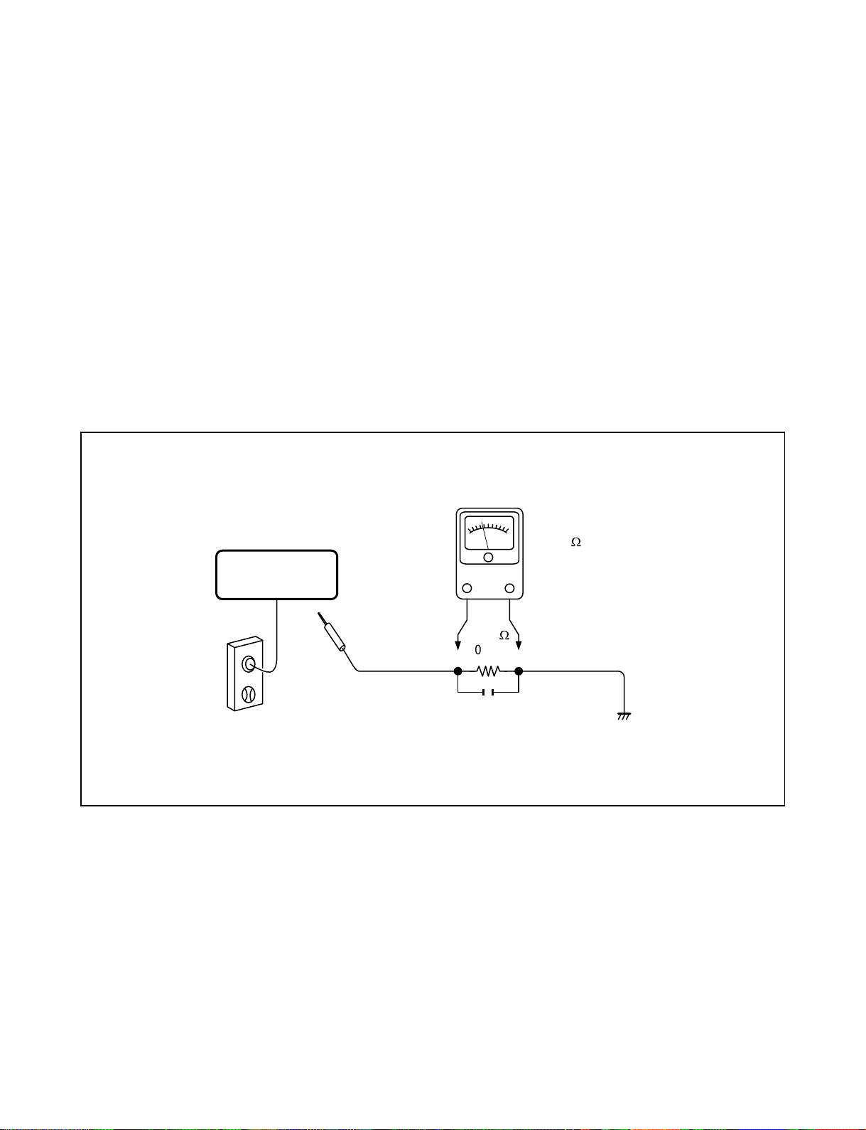
LEAKAGE CURRENT CHECK
Plug the AC line cord directly into a 120V AC outlet (do
not use an isolation transformer for this check). Use an
AC voltmeter, having 5000 Ω per volt or more sensitivity.
Connect a 1500 Ω 10 W resistor, paralleled by a 0.15 µF
150V AC capacitor between a known good earth ground
(water pipe, conduit, etc.) and all exposed metal parts of
cabinet (antennas, handle bracket, metal cabinet
screwheads, metal overlays, control shafts, etc.).
READING SHOULD NOT EXCEED 0.3V
Measure the AC voltage across the 1500 Ω resistor.
The test must be conducted with the AC switch on and
then repeated with the AC switch off. The AC voltage
indicated by the meter may not exceed 0.3 V. A reading
exceeding 0.3 V indicates that a dangerous potential
exists, the fault must be located and corrected.
Repeat the above test with the DVD VIDEO PLAYER
power plug reversed.
NEVER RETURN A DVD VIDEO PLAYER TO THE
CUSTOMER WITHOUT T AKING NECESSAR Y
CORRECTIVE ACTION.
DVD VIDEO PLAYER
AC OUTLET
Test all exposed metal.
Voltmeter Hook-up for Leakage Current Check
1500
W
10 W
0.15 µF 150V AC
AC VOLTMETER
(5000 W per volt
or more sensitivity)
Good earth ground
such as a water pipe,
conduit, etc.
Page 4
SAFETY NOTICE
The lightning flash with arrowhead symbol, within an
equilateral triangle, is intended to alert the user to the
presence of uninsulated “dangerous voltage” within the
product’s enclosure that may be of sufficient magnitude to
constitute a risk of electric shock to persons.
The exclamation point within an equilateral triangle is
intended to alert the user to the presence of important
operating and maintenance (servicing) instructions in the
literature accompanying the appliance.
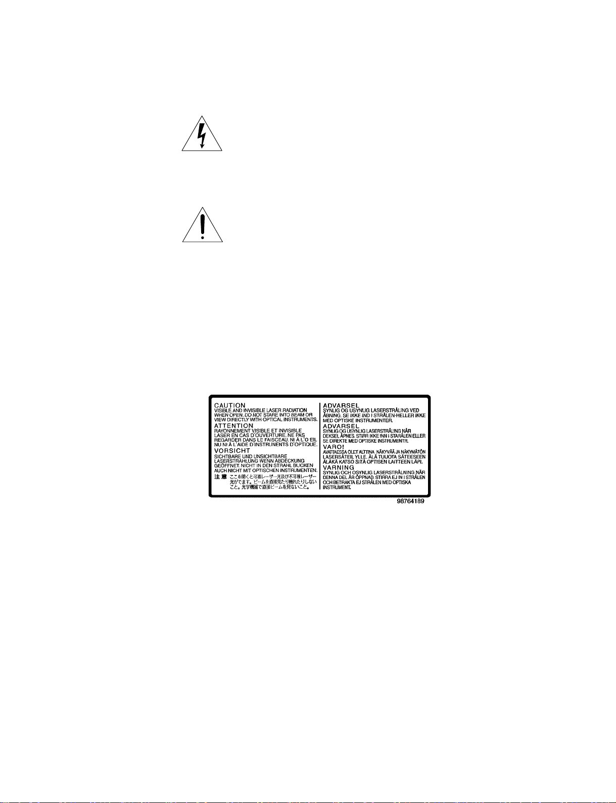
LASER BEAM CAUTION LABEL
When the power supply is turned on, you may not remove this laser caution label. If it is removed, laser radiation
may be recceived.
Page 5

CONTENTS
GENERAL DESCRIPTIONS
1. PREPARATION FOR SERVICING ......................................... 1-1
2. LOCATION OF MAIN PARTS AND
MECHANISM PARTS ............................................................... 1-2
2-1. Location of Main Parts....................................................... 1-2
2-2. Location of Mechanism Parts ............................................ 1-3
SECTION 1
3. TROUBLESHOOTING ............................................................ 1-7
3-1. Main Circuit....................................................................... 1 - 7
3-1-1. Servo System ................................................................. 1- 7
3-1-2. Location Diagram of Servo Test Point .................. 1-14
PART REPLACEMENT AND ADJUSTMENT PROCEDURES
1. REPLACEMENT OF MECHANICAL PARTS ................... 2- 1
1-1. Cabinet Replacement ....................................................... 2 - 1
1-1-1. Top Cover ...................................................................... 2-1
1-1-2. Clamper Stay ................................................................ 2 - 1
1-1-3. Tray Panel ..................................................................... 2 -2
1-1-4. Front Panel and Tray .................................................. 2 - 3
1-1-5. Rear Panel ..................................................................... 2 -3
1-2. PC Board Replacement ................................................... 2- 4
1-2-1. Main PC Board ............................................................. 2-4
1-2-2. Output PC Board ......................................................... 2 - 4
1-2-3. Power PC board ........................................................... 2- 5
SERVICING DIAGRAMS
1. STANDING PC BOARDS FOR SERVICING ..................... 3 - 1
2. CIRCUIT SYMBOLS AND
SUPPLEMENTARY EXPLANATION ..................................... 3-2
2-1. Precautions for Part Replacement .................................... 3-2
2-2. Solid Resistor Indication .................................................... 3-2
2-3. Capacitance Indication ....................................................... 3-2
2-4. Inductor Indication ............................................................. 3-3
2-5. Waveform and Voltage Measurement .............................. 3-3
3. PRINTED WIRING BOARD AND
SCHEMATIC DIAGRAM .......................................................... 3-5
4. BLOCK DIAGRAMS .................................................................. 3-7
4-1. Overall Block Diagram ...................................................... 3-7
4-2. Power Supply Block Diagram ........................................... 3-9
4-3. Front Display, Power Switch Block Diagram ................ 3-10
4-4. Main Block Diagrams .................................................... 3-13
4-5. Output Block Diagram .................................................. 3-17
SECTION 2
1-2-4. Front PC Board ............................................................ 2 - 5
1-3. Mechanism Parts ............................................................... 2- 6
1-3-1. Mechanism Chassis Assembly ..................................... 2-6
1-3-2. Loading Belt .................................................................. 2 -6
1-3-3. Loading Motor .............................................................. 2-7
1-3-4. Sub Chassis (with a pickup mechanism) ................... 2- 7
1-3-5. Pickup Mechanism Assembly ...................................... 2 - 8
1-3-6. Gear A Assembly, Gear B and
Rack Gear Assembly ...................................................... 2-8
1-3-7. Feed Motor ...................................................................... 2-9
SECTION 3
5. CIRCUIT DIAGRAMS ........................................................... 3-19
5-1. Power Supply Circuit Diagram.................................... 3-19
5-2. Front Display, Power Switch Circuit Diagram......... 3-21
5-3. Main Circuit Diagram ................................................... 3-24
5-4. Output Circuit Diagram................................................ 3-29
5-5. Motor System Circuit Diagrams .................................. 3-34
6. PC BOARDS ............................................................................ 3-35
6-1. Power Supply PC Board................................................ 3-35
6-2. Main PC Board ............................................................... 3-37
6-3. Output PC Board............................................................ 3-47
SAFETY PRECAUTION ............................................................... 4 - 1
NOTICE ............................................................................................ 4- 1
ABBREVIATIONS .......................................................................... 4- 1
1. Integrated Circuit (IC) ........................................................ 4- 1
2. Capacitor (Cap) .................................................................... 4-1
3. Resistor (Res) ......................................................................... 4- 1
SECTION 4
PARTS LIST
4. EXPLODED VIEWS ................................................................. 4 - 2
4-1. Packing Assembly ............................................................. 4 - 2
4-2. Chassis Assembly ............................................................... 4- 3
4-3. Mechanism Assembly........................................................ 4 - 4
5. PARTS LIST ............................................................................... 4- 6
Page 6

-
Page 7
GENERAL DESCRIPTIONS
S
GENERAL DESCRIPTIONS
SECTION 1
GENERAL DESCRIPTIONS
1. PREPARATION FOR SERVICING
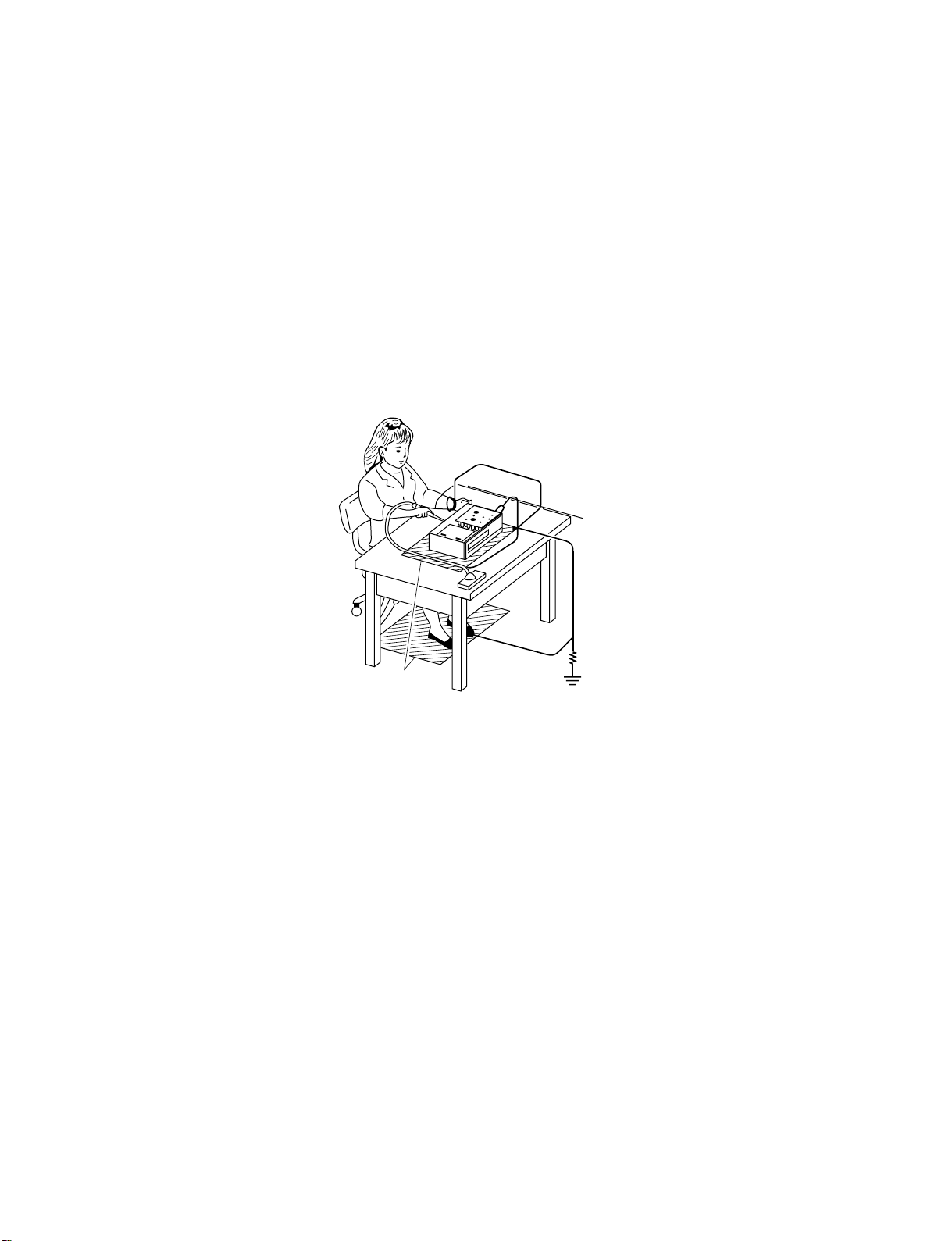
The Pickup Head consists of a laser diode that is very susceptible to external static electricity.
Although it may operate properly after replacement, if subjected to electrostatic discharge during replacement,
its life might be shortened. When replacing the laser diode, LSI's and IC's, use a conductive mat, soldering iron
with ground wire, etc. to protect against damage from static electricity.
Ground conductive
wrist strap for body.
oldering iron
with ground wire
or ceramic type
SECTION 1
1MΩ
Conductive mat
The ground resistance
between the ground line
and the ground is less than 10Ω.
1-1
Page 8
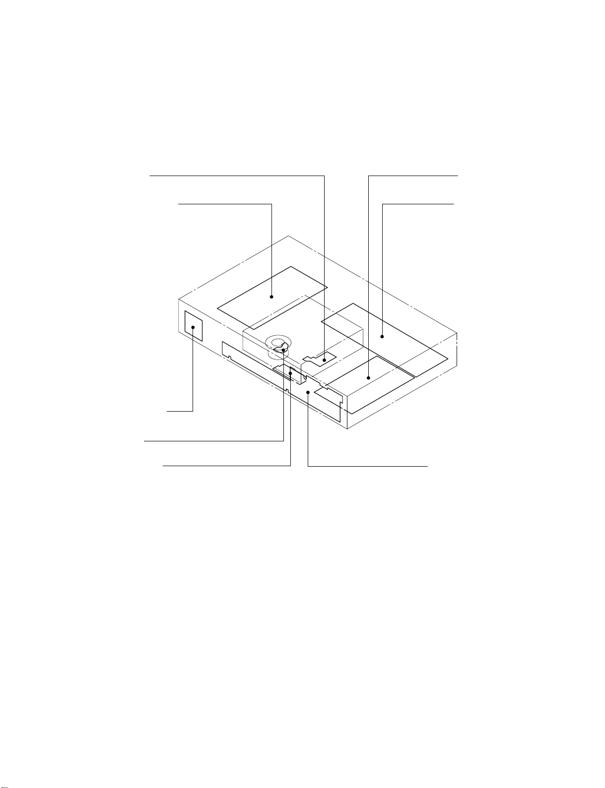
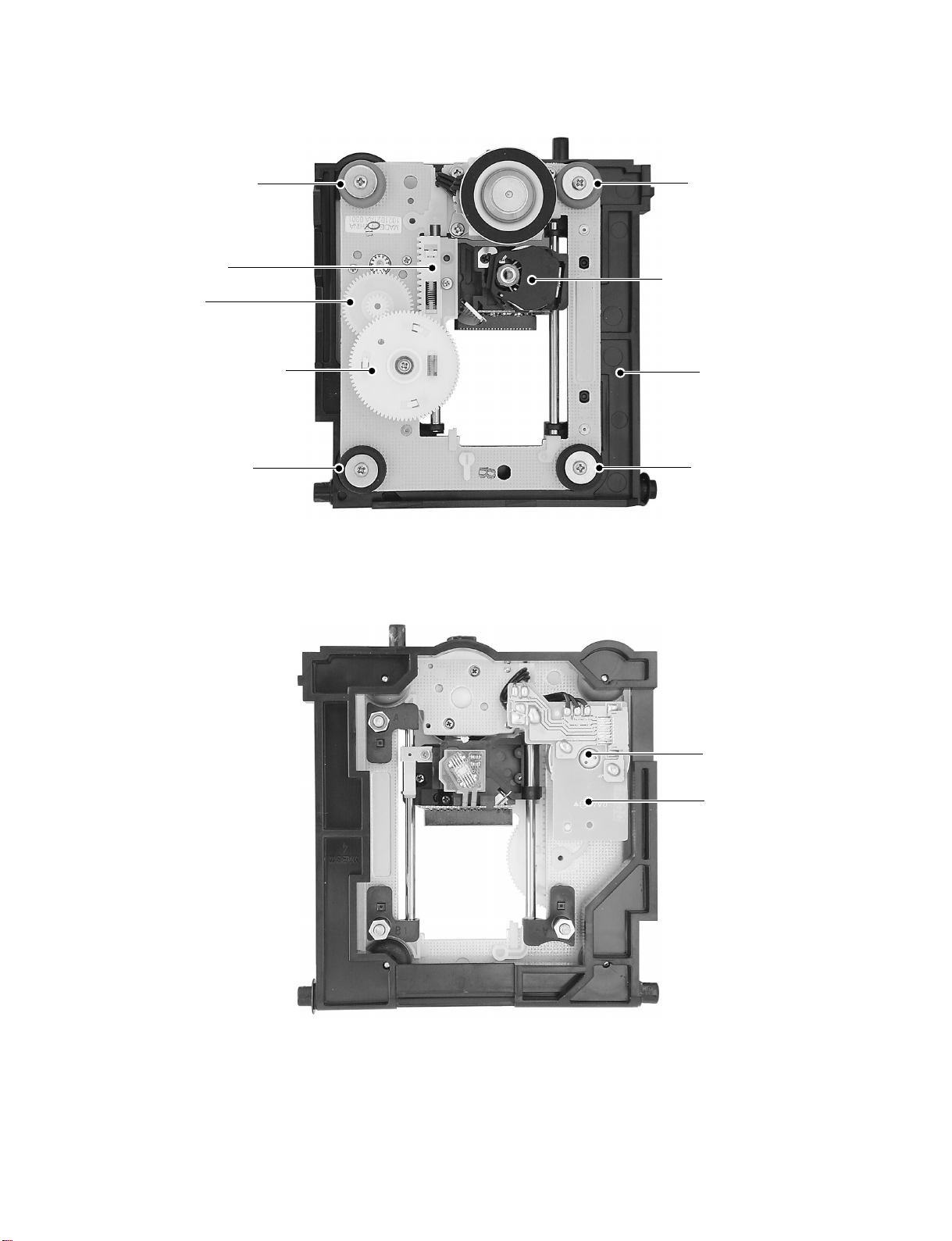
2. LOCATION OF MAIN PARTS AND MECHANISM PARTS
2-1. Location of Main Parts
Feed motor PC board
EU02 Power supply PC board
EU04 Power SW PC board
Disc motor PC board
EU01 Main PC board
EU05 Output PC board
Loading motor PC board
EU03 Front display PC board
Fig. 1-2-1
1-2
Page 9
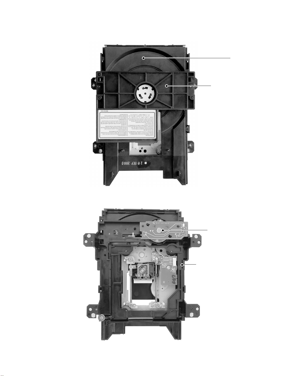
2-2. Location of Mechanism Parts
y
y
r
Tra
Clamper sta
Fig. 1-2-2 Mechanism chassis assembly (Top side)
Loading moto
PC board
Mechanism chassis
Fig. 1-2-3 Mechanism chassis assembly (Bottom side)
1-3
Page 10
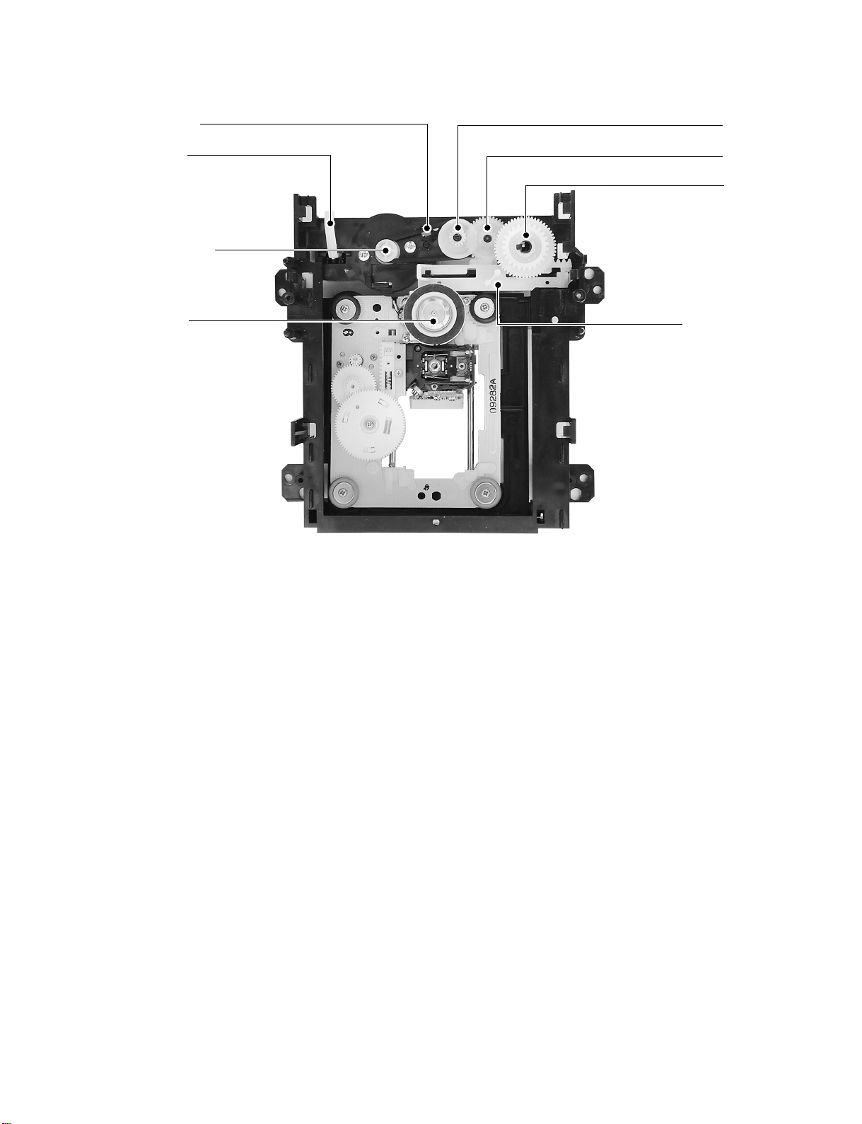
Loading belt
r
r
r
r
Gea
Kick lever
Loading motor
Disc motor
Gea
Gea
Cam Slide
Fig. 1-2-4 Mechanism chassis assembly (Internal side)
1-4
Page 11
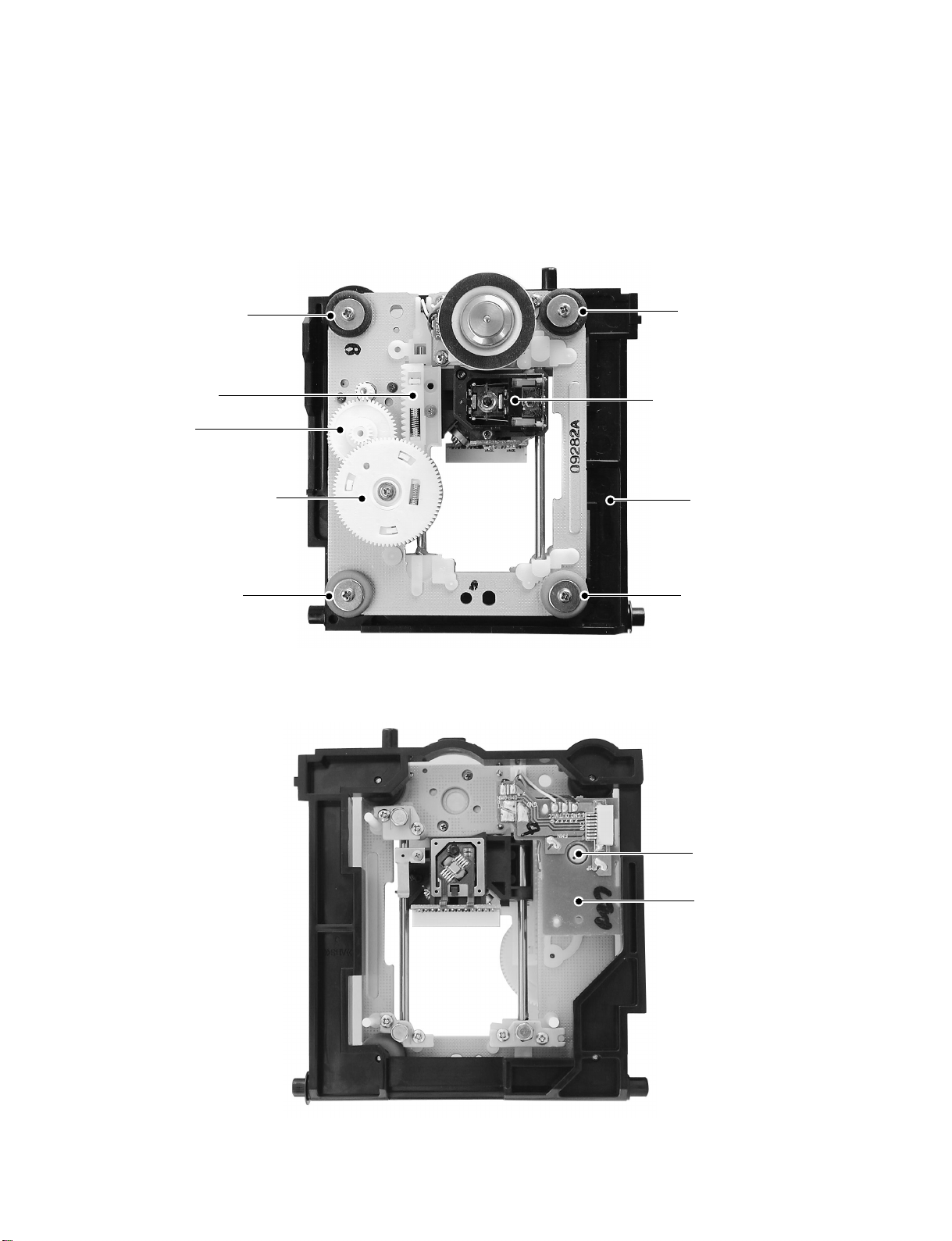
r
r
r
r
d
<Type A>
Note:
When servicing, note that this model has two types of
pickup mechanism assembly.
Type A is a service part. Type B can be replaced with a Type A pickup.
Front damper
Rack gear
assembly
Gear A
Gear B assembly
Rear damper
Front dampe
Pickup assembly
Sub chassis
Rear dampe
Fig. 1-2-5 Pickup mechanism chassis assembly (Top side)
Fig. 1-2-6 Pickup mechanism chassis assembly (Bottom side)
1-5
Feed moto
Feed moto
PC boar
Page 12
<Type B>
r
r
r
r
d
Front damper
Rack gear
assembly
Gear A
Gear B assembly
Rear damper
Front dampe
Pickup assembly
Sub chassis
Rear dampe
Fig. 1-2-7 Pickup mechanism chassis assembly (Top side)
Fig. 1-2-8 Pickup mechanism chassis assembly (Bottom side)
1-6
Feed moto
Feed moto
PC boar
Page 13
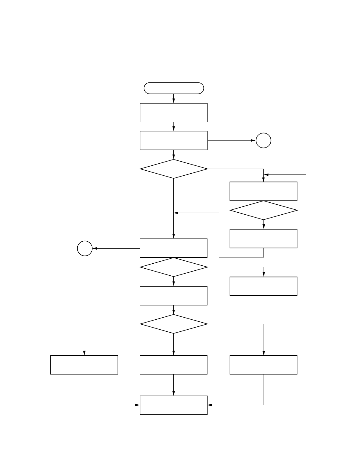
3. TROUBLESHOOTING
3-1. Main Circuit
3-1-1. Servo System
(1) Initial Operation after Power ON
Power ON
Send each LSI hard RST
command and initial command.
Pickup head is positioned at
transmission initial position.
Is tray closed?
Pin 5 of CN502,
TCLS=L
Y
2
NG
Disc presence/absence and
disc judgement
Is a disc present?
Y
DVD or CD initial setting.
N
Tray close operation
Pin C9 of IC306 (E537): LDMP = H/L
Pin Y19 of IC306 (E538): LDMN = L
Tray stops.
Pin C9 of IC306 : LDMP = H
Pin Y19 of IC306 : LDMN = L
N
Laser OFF
Display: INSERT DISC
Monitor screen: NO DISC
1
Is tray closed?
Pin 5 of CN502:
TCLS = L
Y
N
DVD single (single-layer)
DVD single
Initial setting.
DVD single
(single-layer)/DVD dual
(dual-layer)/CD?
DVD dual (dual-layer)
DVD dual
Initial setting.
To each disc playback process.
Fig. 1-3-1
1-7
CD
CD
Initial setting.
Page 14
1
Pickup (P.U.) transmission initial
operation does not occur.
The pickup transmission initial operation is carried out to
determine the initial position by transmitting the pickup to the
innermost position once (start-limit switch (pin 4 of CN503)
develops "L".) and to the external direction at low speed
(start-limit switch develops "H", turning off the switch.).
Does pulse of
1.65V 1.65V develop at
pin 162 of IC401?
Y
Check feed gear.
N
Check BUS between IC401-IC306
and oscillation.
Fig. 1-3-2
2-1
"No disc" misjudgement display of
N
disc presence.
Does lens move with
UP/DOWN full stroke in
focus direction?
Y
N
3
Does focus search
voltage of 1.65V 0.4V develop
at pin 23 of IC503 (E544)?
Y
Does search signal
output at both edges of focus coil?
(Pins 15 to 18 of CN501)
Y
Check pickup head
and wiring.
Is laser current normal?
Y
Does RFSB signal
develop more than 0.3V?
Y
Check peripheral
circuit of IC306.
N
N
Check IC401.
Check IC503.
Fig. 1-3-3
N
Check IC502.
Lens cleaning.
Replace pickup head.
1-8
Page 15
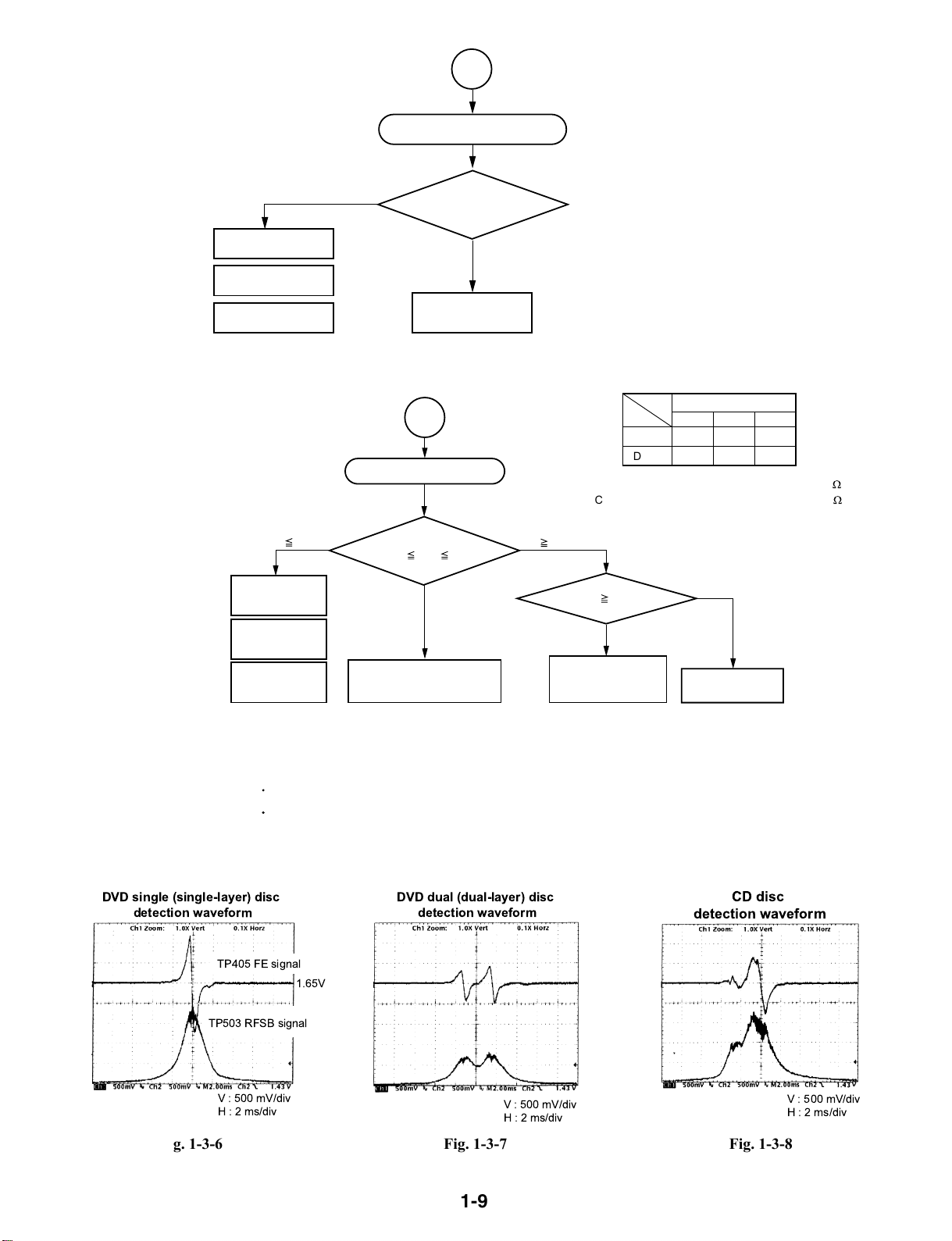
2-2
V : 500 mV/div
H : 2 ms/div
CD disc
detection waveform
Disc kind misjudgement
(Initial setting is NG.)
N
Check IC502.
Lens cleaning.
Replace pickup head.
Are FE and RFSB
signals for each disc normal?
Y
Check peripheral
circuit of IC306.
Fig. 1-3-4
3
DVD Iop
Check laser operating current.
lop I min
Check wiring for
pickup head.
Check pins 13, 14
and 15 of IC502
serial bus.
Check peripheral
circuits of IC502,
Q501, Q502.
To turn on each laser diode forcibly, press the following buttons on the remote controller.
DVD LD:
CD LD:
After checked the laser current, press POWER or OPEN/CLOSE button to turn it off.
CAUTION
The laser ray emitting out from the pickup head is very harmful to your eyes.
Keep your eyes from the objective lens at least 300mm distance during the pickup head operating.
When you perform solder removal work, please turn OFF a set power supply and perform the
ground of human body and a tool.
ZOOM, 0, 3, 0, ZOOM
ZOOM, 0, 3, 1, ZOOM
Check laser current.
I min lop I max
Y
Check FE and RFSB signal
lop I max
Check solder removal
of the short land for
laser diode protection.
CD Iop
DVD Iop = Voltage between (E559 and E534) /10
CD Iop = Voltage between (E536 and E534) /10
lop 200 mA
Y
Laser operating current
min
typ max
20mA
35mA
60mA
20mA
45mA
80mA
N
Replace pickup
mechanism.
W
W
DVD single (single-layer) disc
detection waveform
Fig. 1-3-5
DVD dual (dual-layer) disc
detection waveform
TP405 FE signal
1.65V
TP503 RFSB signal
V : 500 mV/div
H : 2 ms/div
V : 500 mV/div
H : 2 ms/div
Fig. 1-3-6 Fig. 1-3-7 Fig. 1-3-8
1-9
Page 16
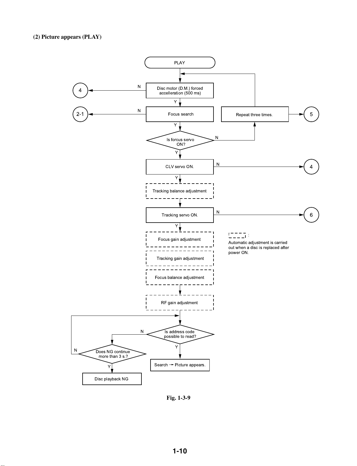
(2) Picture appears (PLAY)
PLAY
4
2-1
N
N
Disc motor (D.M.) forced
accelleration (500 ms)
Focus search
Is forcus servo
CLV servo ON.
Tracking balance adjustment
Tracking servo ON.
Focus gain adjustment
Tracking gain adjustment
Y
Y
Y
Y
Y
ON?
Repeat three times.
N
N
N
:
Automatic adjustment is carried
out when a disc is replaced after
power ON.
5
4
6
Focus balance adjustment
RF gain adjustment
N
N
Does NG continue
more than 3 s.?
Y
Disc playback NG
Is address code
possible to read?
Y
Search Picture appears.
Fig. 1-3-9
1-10
Page 17
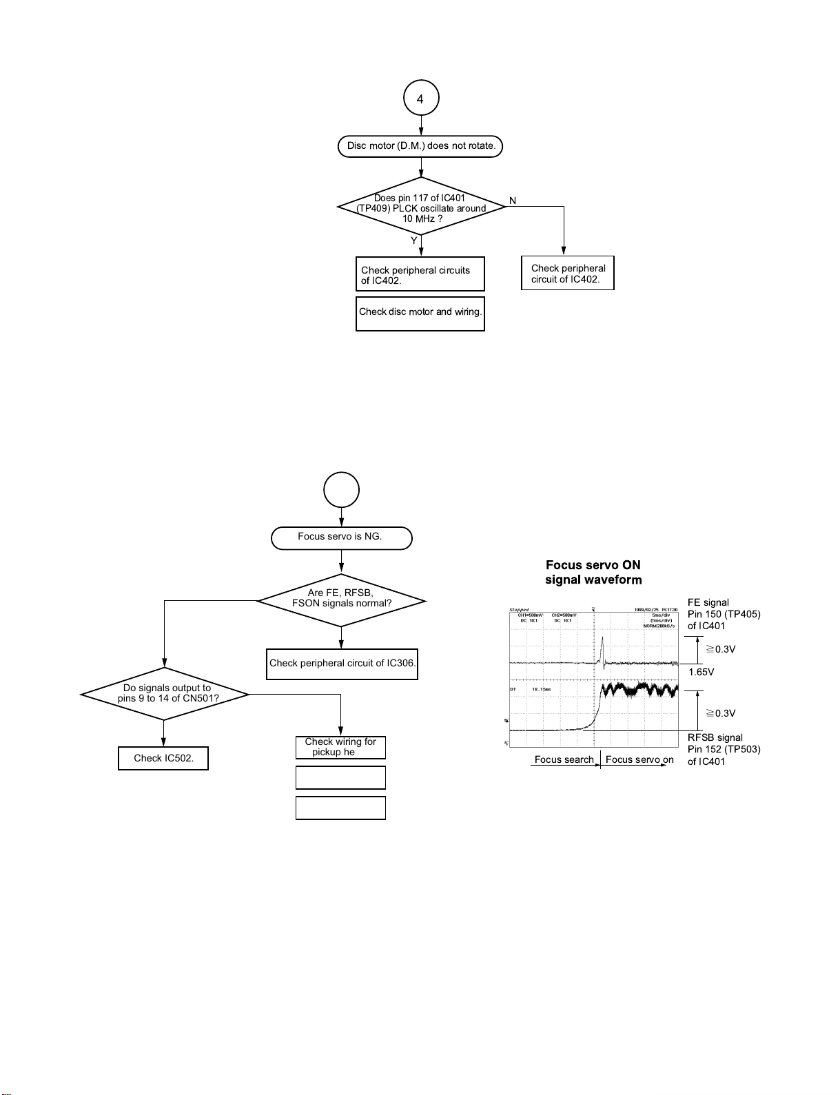
4
Disc motor (D.M.) does not rotate.
Does pin 117 of IC401
(TP409) PLCK oscillate around
10 MHz ?
Check peripheral
circuit of IC402.
Check peripheral circuits
of IC402.
Check disc motor and wiring.
N
Y
Do signals output to
pins 9 to 14 of CN501?
Y
Check IC502.
5
Focus servo is NG.
N
N
Are FE, RFSB,
FSON signals normal?
Y
Check peripheral circuit of IC306.
Check wiring for
pickup head.
Lens cleaning.
Replace pickup
mechanism.
Fig. 1-3-10
Focus servo ON
signal waveform
Focus search Focus servo on
Fig. 1-3-12
FE signal
Pin 150 (TP405)
of IC401
0.3V
1.65V
0.3V
RFSB signal
Pin 152 (TP503)
of IC401
Fig. 1-3-11
1-11
Page 18
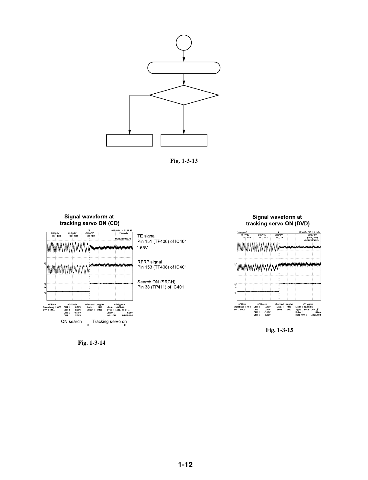
6
Signal waveform at
tracking servo ON (DVD)
Tracking servo is NG.
Signal waveform at
tracking servo ON (CD)
Check IC502.
TE signal
Pin 151 (TP406) of IC401
1.65V
RFRP signal
Pin 153 (TP408) of IC401
N
Is TE signal normal?
Y
Check peripheral
circuit of IC306.
Fig. 1-3-13
ON search Tracking servo on
Search ON (SRCH)
Pin 38 (TP411) of IC401
Fig. 1-3-15
Fig. 1-3-14
1-12
Page 19
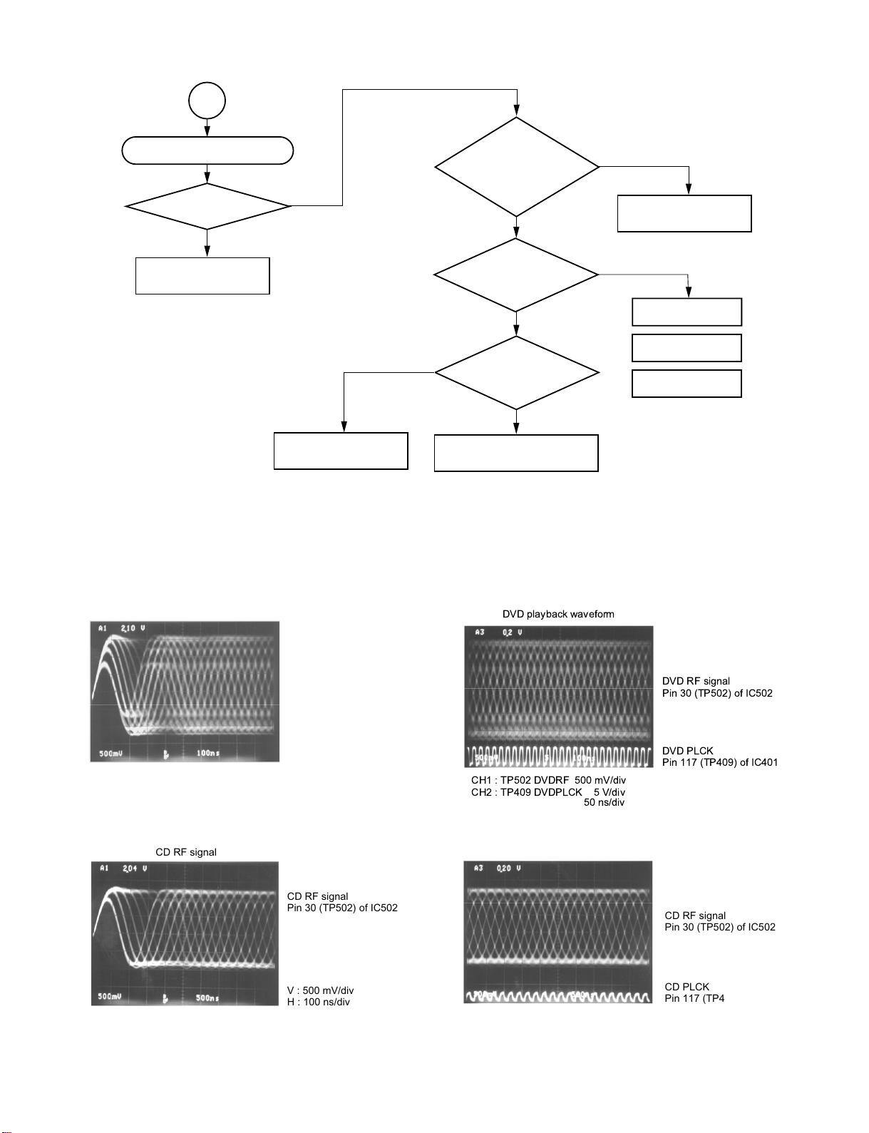
7
Disc playback is NG (DVD).
Is PLL locked?
(Refer to waveforms.)
Y
Check signal process
system following to IC402.
N
Check peripheral circuits of
IC401 and IC306.
N
Fig. 1-3-16
Does pulse of
L = 1.65V and H = 3.3V
develop at pin 131 and
L = 0V and H = 1.65V
develop at pin 132
of IC401?
Y
Does RF output
higher than 1 V(p-p)
develop at pin 30 (TP502)
of IC502?
Y
Pin 43 of IC502 = 2.4V
Pin 44 of IC502 = 3.0V
Y
Check peripheral circuits
of IC502 and IC401.
N
Check peripheral circuits
of IC401 and IC306.
N
Check IC502.
Lens cleaning.
Pickup mechanism
replacement
DVD RF signal
Fig. 1-3-17
CD RF signal
DVD RF signal
Pin 30 (TP502) of IC502
V : 500 mV/div
H : 50 ns/div
CD RF signal
Pin 30 (TP502) of IC502
PLL works as a servo loop to generate a clock signal for reading RF
signal binary data. With the PLL locked, the eye pattern is identified
clearly when triggered with the read clock PLCK.
DVD playback waveform
DVD RF signal
Pin 30 (TP502) of IC502
DVD PLCK
Pin 117 (TP409) of IC401
CH1 : TP502 DVDRF 500 mV/div
CH2 : TP409 DVDPLCK 5 V/div
50 ns/div
Fig. 1-3-19
CD playback waveform
CD RF signal
Pin 30 (TP502) of IC502
Fig. 1-3-18
V : 500 mV/div
H : 100 ns/div
1-13
CH1 : TP502 CDRF 500 mV/div
CH2 : TP409 CDPLCK 5 V/div
100 ns/div
Fig. 1-3-20
CD PLCK
Pin 117 (TP409) of IC401
Page 20
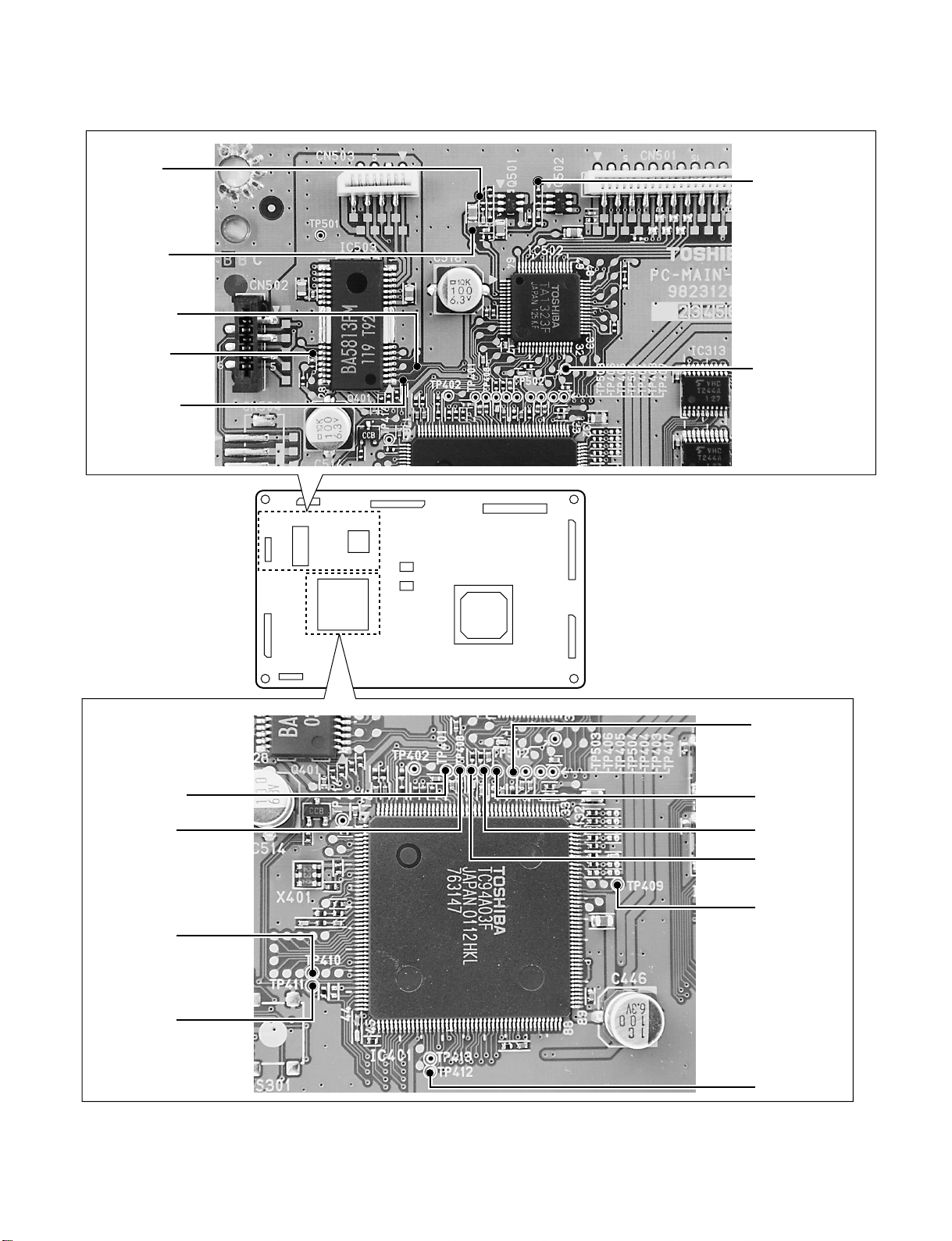
3-1-2. Location Diagram of Servo Test Point
E536 CD
E534 +5V
E538 LDMN
E544 FOO
E537 LDMP
CN502
CN603
IC503
CN503
IC401
IC502
CN501
IC313
IC312
E559 DVD
TP502 RFO
CN701
CN901
IC306
TP401 VRFED
TP408 RFRP
TP410 FLGA
TP411 FLGB
CN302
CN601
TP504 RFCT
TP405 FE
TP406 TE
TP503 RFSB
TP409 PLCK
TP412 VMCK
Fig. 1-3-21
1-14
Page 21

SECTION 2
PART REPLACEMENT AND
ADJUSTMENT PROCEDURES
CAUTIONS BEFORE STARTING SERVICING
Electronic parts are susceptible to static electricity and may easily damaged, so do not forget to take a proper grounding
treatment as required.
Many screws are used inside the unit. To prevent missing, dropping, etc. of the screws, always use a magnetized screwdriver in servicing. Several kinds of screws are used and some of them need special cautions. That is, take care of the
tapping screws securing molded parts and fine pitch screws used to secure metal parts. If they are used improperly, the
screw holes will be easily damaged and the parts can not be fixed.
1. REPLACEMENT OF MECHANICAL PARTS
1-1. Cabinet Replacement
1-1-1. Top Cover
1. Remove five screws (1) and remove the top cover (2).
Screw (1)
Top cover (2)
Screws (1)
Screw (1)
1-1-2. Clamper Stay
<Removal>
1. Remove two screws (1).
2. Release two claws and remove the clamper stay (2).
Screws (1)
Clamper stay (2)
Clamper
stay (2)
Claw
A
Clamper stay (2)
Claw
Fig. 2-1-1
2-1
Spring
Claws
Fig. 2-1-2
Page 22

<Mounting >
1. The spring for tray side pressure is inserted into the
portion “A”. (Refer to Fig. 2-1-2.)
2. By referring to Fig. 2-1-3, insert the spring normally
and mount the clamper stay.
This part should be touch
to the left side of the tray.
NG
1-1-3. Tray Panel
<Tray Ejection>
1. Slide the slider (2) of the mechanism chassis assembly
(1) with a screwdriver, etc. in the arrow direction, so
that the tray (3) is ejected.
Note:
• Take care not to damage the pickup and other parts.
OK
Mechanism
chassis assembly
Press down by finger
unitil fix the clamper assembly
No floating
OK
Fig. 2-1-3
NG
Spring
Floating NG
Tray
NG
Screw
driver
Slider (2)
Mechanism
chassis assembly (1)
Tray (3)
Front panel
Fig. 2-1-4
<Tray Panel Removal>
1. Eject the tray (3).
2. Twist the tray panel (4) a little in the arrow A direction
with the tray (3) hold by hand to release two claws and
lift up the tray panel (4) in the arrow B direction, then
the tray panel (4) is removed.
(Refer to Fig. 2-1-5.)
3. When mounting the tray panel (4), insert the tray panel
(4) along the grooves of the both sides of the tray (3)
until clicking.
2-2
Page 23

Tray (3)
Slider
Pickup mechanism
assembly
Tray (3)
Gear (4)
Gear (4)
Triangle mark
Triangle mark
Marking
Gear (4)
Position of the line
Fig. A
Fig. B
Tray rack gear
• Confirm that the mark of the gear matches with the
triangle mark on the reverse side of the tray in the tray
close status. (The gear is rotated with the slider locks.)
B
(Refer to Fig. B.)
Tray panel (4)
Tray (3)
A
Claws
Tray panel (4)
Fig. 2-1-5
1-1-4. Front Panel and Tray
1. Remove the flexible cable (1).
2. Remove one screw (2) and remove the GND lead (5).
3. Release four claws and remove the front panel (4).
4. Pull out the tray (3) to this side.
Screw (2)
GND lead (5)
Note:
Claw
Tray (3)
Front
panel (4)
Claws
Flexible cable (1)
Fig. 2-1-6
• Insert the tray (3) with the front side of the pickup
mechanism assembly descended. (The slider positions
to the left side.)
• The gears are required to match their phases each
other. After setting the gear (4) as shown in the figure
“A”, insert the tray (3). When inserting a tray (3), push
the rack gear side shown by the arrow.
Fig. 2-1-7
1-1-5. Rear Panel
1. Remove eight screws (1) and remove the rear panel (2).
Screws (1)
Rear panel (2)
Fig. 2-1-8
2-3
Page 24

1-2. PC Board Replacement
1-2-1. Main PC Board
Note:
• Before removing the main PC board (4), be sure to
short-circuit the laser diode output land.
After replacing, open the land as it was after inserting
the flexible cables (1).
1. Remove the top cover. (Refer to item 1-1-1.)
2. Remove six flexible cables (1) and remove one
connector (2).
3. Remove four screws (3).
4. Remove the main PC board (4).
Note:
• When mounting, be sure to twist the wire for the
connector (2) several times.
Twist more than 7 times.
Connector (2)
Flexible
cables (1)
Screws (3)
Flexible cables (1)
1-2-2. Output PC board
1. Peel off the tape (1).
2. Remove the connector (2).
3. Disconnect two flexible cables (3).
4. Remove three screws (4).
5. Remove five screws (5) and remove the output PC
board (6).
Note:
• When mounting, be sure to twist the wire for the
connectors (2) several times.
Twist more than 9 times.
Screws (4)
Connector (2)
Tape (1)
Output
PC board (6)
Main
PC board (4)
Pickup head
Laser diode
output lands
Type A Type B
Pickup head
Laser diode
output lands
Flexible
cables (1)
Screws (5)
Flexible cables (3)
Fig. 2-1-10
Fig. 2-1-9
2-4
Page 25

1-2-3. Power Supply PC Board
Power SW
PC board (5)
Front display
PC board (3)
Screws (2)
Screws (2)
1. Peel off the tape (1).
2. Remove the connectors (2) and (3).
3. Remove three screws (4).
4. Remove two screws (5).
5. Remove the power supply PC board (6).
Note:
• When mounting, be sure to twist the wire for the
connectors (2) and (3) several times.
1-2-4. Front PC Board
1. Remove the front panel. (Refer to item 1-1-4.)
2. Remove one flexible cable (1).
3. Remove six screws (2) and remove the front display
PC board (3).
4. Remove two screws (4) and remove the power switch
PC board (5).
5. Remove three screws (6) and the ENTER switch (7).
Screws (4)
Connector (3)
Twist more than 9 times.
Power supply
PC board (6)
Tape (1)
Screws (5)
Connector (2)
Fig. 2-1-12
Twist more than 7 times.
Fig. 2-1-11
2-5
Page 26

1-3. Mechanism Parts
1-3-1. Mechanism Chassis Assembly
Note:
• When removing the mechanism chassis assembly (3),
be sure to short-circuit the laser diode output land
before removing the connector and the flexible cables.
After replacing, open the land as it was after inserting
the connector and flexible cables.
1. Remove the tray . (Refer to items 1-1-3 and 1-1-4.)
2. Remove three flexible cables (1).
3. Remove four screws (2) and remove the mechanism
chassis assembly (3).
1-3-2. Loading Belt
1. Remove the gear (1) by releasing the claw.
2. Remove the gear (2).
3. Remove the gear (3) and the loading belt (4).
4. Replace the loading belt (4) with a new one.
5. When mounting, perform the reverse order of the
removal.
Note:
• When mounting the loading belt (4), twisting and
attaching of a grease, etc. are not allowed.
Gear (1)
Screws (2)
Flexible
cable (1)
Mechanism
chassis assembly (3)
Flexible
cables (1)
Type A
Pickup head
Laser diode
output lands
Type B
Pickup head
Laser diode
output lands
Gear (2)
Loading belt (4)
Gear (3)
Claw
Mechanism
chassis assembly
Fig. 2-1-14
Fig. 2-1-13
2-6
Page 27

Screw (2)
Boss A
Washer
Washer (3)
Sub chassis (4)
(with the pickup mechanism attached)
Boss C
Boss B
Cam slider
up/down cam (5)
Groove
Claw
Groove
Mechanism chassis
assembly (1)
Boss A
Claw
Boss B
Groove
1-3-3. Loading Motor
1. Remove the loading belt. (Refer to item 1-3-2.)
2. Remove two screws (1) and two claws. Then remove
the loading motor (2) (with the loading motor PC
board (3) attached).
3. Desolder the terminal section of the loading motor (2)
and remove the loading motor PC board (3).
4. Replace the loading motor (2) with a new one.
5. When mounting, perform the reverse order of the
removal.
Note:
• When replacing the loading motor , meet the polarity
phase of the terminals. (Mount the motor with the
label positioned as shown in Fig. 2-1-15.)
Screws (1)
1-3-4. Sub Chassis (with a pickup mechanism)
1. Turn the mechanism chassis assembly (1) upside down.
2. Remove one screw (2) and one washer (3) release the
boss “A” from the claw. Then remove the sub chassis (4)
(with the pickup mechanism) by sliding in the arrow
direction.
3. When mounting, perform the reverse order of the
removal.
Note:
• When mounting the sub chassis (4) (with the pickup
mechanism), first, insert the boss “C” along the groove
of the cam slider up/down cam (5) and next, the boss
“B” and “A”.
• The boss “A” may be used with washers. (One or two
washers are used to prevent from the slust rattling. In
some cases, no washer is used.)
When the washer(s) is used, be sure to assemble as it
was without losing.
Fig. 2-1-15
Mechanism
chassis assembly
Loading motor (2)
Claws
Desolder
Motor label
side
Loading motor
PC board (3)
Fig. 2-1-16
2-7
Page 28

r
1-3-5. Pickup Mechanism Assembly
<Removal>
1. Remove four screws (1) and four washers (2) then
remove the pickup mechanism assembly (3).
<Mounting>
1. Replace the pickup mechanism assembly (3) with a
new one.
2. When mounting, perform the reverse order of the
removal.
Screws (1)
1-3-6. Gear B Assembly, Gear A and Rack Gear
Assembly
<Removal>
1. Remove one screw (3) and remove the gear B assembly
(1).
2. Remove the gear A (2).
3. Remove one screw (5) and remove the rack gear
assembly (4).
Screw (5)
Screw (3)
Gear B
assembly (1)
Washars (2)
Damper
Damper
(Black)
Damper
(Black)
Fig. 2-1-17
(Blue)
Pickup mechanism
assembly (3)
Dampe
(Blue)
Note:
• The dampers’ color differs when used for the front
side and the rear.
• When mounting the pickup mechanism assembly (2)
with the screws (1), push the pickup mechanism assembly (2) downward without being caught and tighten the
screws (1) after placing the washer with the damper bent.
Screw (1)
Rack gear
assembly (4)
Gear A (2)
Pickup mechanism
assembly
Fig. 2-1-19
<Mounting>
1. When mounting, perform the reverse order of the
removal.
2. Mount the gear B assembly (1) by pushing the pickup
head (5) to the disc motor side (arrow A direction) and
shifting the upper gear of the rack gear assembly (4) in
the arrow B direction. (Refer to Fig. 2-1-20.)
3. Fit the positioning holes on the upper gear and lower
gear of the gear B assembly (1) and mount on the
pickup mechanism assembly with the phase matched.
At this time, note that the phase of the gear B assembly (1) and the gear A (2) shows the status in the Fig.
2-1-21.
Pickup mechanism
assembly (2)
Damper
Washer (2)
Fig. 2-1-18
2-8
Page 29

Pickup Head (5)
Pickup mechanism
assembly
B
Positioning holes
Gear B assembly (1)
A
Rack gear assembly (4)
Fig. 2-1-20
Gear A (2)
1-3-7. Feed Motor
<Removal>
1. Remove the gear B assembly and the gear A. (Refer to
item 1-3-6.)
2. Remove two screws (1) and remove the feed motor (2)
(with the feed motor PC board (3) attached).
(Refer to Fig. 2-1-22.)
3. Desolder the terminals of the feed motor (2) and
remove the feed motor PC board (3).
<Mounting>
1. Tighten the feed motor (2) on the pickup mechanism
assembly with two screws (1).
2. Insert the feed motor PC board (3) with the positioning pin on the chassis matched and solder the terminals.
3. Perform the reverse order of the removal.
Note:
• Mount the gear B assembly (1) and the gear A (2) with
their gear teeth placed more than one tooth at least
inside the shaded portion.
Innermost position
of pickup head
Rack gear assembly (4)
Gear A (2)
Within the position shown
by the shaded porition.
Gear B assembly (1)
Fig. 2-1-21
Note:
• After mounting, put the lead wires through the notch
of the pickup mechanism assembly .
• When replacing the loading motor, meet the polarity
phase of the terminals. (Mount the motor with the
label positioned as shown in Fig. 2-1-22.)
Screws (1)
Pickup mechanism
assembly
Notch
Lead wires
Feed motor (2)
Motor label side
Desolder
2-9
Feed motor
PC board
Fig. 2-1-22
Page 30

2-10
Page 31

SECTION 3
SERVICING DIAGRAMS
1. STANDING PC BOARDS FOR SERVICING
EU02 Power supply PC board
EU04 Power SW PC board
EU05 Output PC board
EU03 Front display PC board
EU01 Main PC board
Fig. 3-1-1
3-1
Page 32

2. CIRCUIT SYMBOLS AND SUPPLEMENTARY EXPLANATION
100k
Rated Wattage Type Tolerance
100
m
Temperature
response
Rated
voltage
Tolerance
2-1. Precautions for Part Replacement
• In the schematic diagram, parts marked
(ex.
F801) are critical part to meet the safety regulations,
so always use the parts bearing specified part codes
(SN) when replacing them.
2-2. Solid Resistor Indication
Unit None ...........Ω
Tolerance None ...........±5%
Rated Wattage (1) Chip Parts
Type None ...........Carbon film
K ...........kΩ
M ...........MΩ
B ...........±0.1%
C ...........±0.25%
D ...........±0.5%
F ...........±1%
G ...........±2%
K ...........±10%
M ...........±20%
None.........1/16W
(2) Other Parts
None.........1/6W
Other than above, described in the Circuit Diagram.
S ...........Solid
R ...........Oxide metal film
W ...........Metal film
W ...........Cement
FR ...........Fusible
• Using the parts other than those specified shall violate
the regulations, and may cause troubles such as
operation failures, fire etc.
Eg. 1
FIg. 3-2-1
2-3. Capacitance Indication
Symbol
Unit None ...........F
Rated voltage None ...........50V
Tolerance (1) Ceramic, plastic, and film capacitors of which
Temperature characteristic None ...........SL
(Ceramic capacitor) For others, temperature characteristics are
Static electricity capacity Sometimes described with abbreviated letters as
(Ceramic capacitor) shown in Eg. 3.
+
...........Electrolytic, Special electrolytic
NP
...........Non polarity electrolytic
...........Ceramic, plastic
M
...........Film
...........Trimmer
µ ...........µF
p ...........pF
For other than 50V and electrolytic capacitors,
described in the Circuit Diagram.
capacitance are more than 10 pF.
None ...........±5% or more
B ...........±0.1%
C ...........±0.25%
D ...........±0.5%
F ...........±1%
G ...........±2%
(2) Ceramic, plastic, and film capacitors of which
capacitance are 10 pF or less.
None ...........more than ±5% pF
B ...........±0.1 pF
C ...........±0.25 pF
(3) Electrolytic, Trimmer
Tolerance is not described.
described. (For capacitors of 0.01 µF and
no indications are described as F.)
Eg. 2
Fig. 3-2-2
Eg. 3
104
4
10x10
pF (0.1µF)
Temperature characteristic
(or Temperature characteristic+
Static electricity capacity tolerance)
Fig. 3-2-3
3-2
Page 33

2-4. Inductor Indication
Type name
10
µ
Type Tolerance
Unit None ...........Η
µ ...........µH
m ...........mH
Tolerance None ...........±5%
B ...........±0.1%
C ...........±0.25%
D ...........±0.5%
F ...........±1%
G ...........±2%
K ...........±10%
M ...........±20%
2-5. Waveform and Voltage Measurement
• The waveforms for CD/DVD and RF shown in the
circuit diagrams are obtained when a test disc is
played back.
• All voltage values except the waveforms are expressed
in DC and measured by a digital voltmeter.
2-6. Others
• The parts indicated with "NC" or "KETU" etc. are not
used in the circuits of this model.
Eg. 4
Fig. 3-2-4
Eg. 5
Fig. 3-2-5
3-3
Page 34

3-4
Page 35

3. PRINTED WIRING BOARD AND SCHEMATIC DIAGRAM
CNY02
Board-in
VCC+12V
VDD+5V
VCC+9V
VEE-9V
E+6V
GND
GND
7654321
7P
Press-fit
VCC+12V
VCC+9V
CN802
EU02
POWER
E+6V
GND
CN801
Board-in
VEE-9V
GND
7654321
VDD+5V
VDD+5V
VDD+3.3V
VDD+2.5V
VKK-34V
EU04 POWER-SW
PWON
E+5V
E+6V
GND
GND
M+8V
MGND
Mechanism
1
2
3
4
5
6
7
8
9
10
11
12
F-
13
F+
EU05 OUTPUT
FFC 1mm 26P
L=120
W501
FFC 1mm 23P
23
VCC
MON2
VOR2
VREF
LDMP
TOPN
LDMN
TCLS
TRAY
DMFG
W102
GND
E+5V
GND
VCC
VCC
GND
MON
VOR
GND
FMN
FMP
GND
LMT
DMN
DMP
VCC
1
RF
2
LD2
3
4
5
6
7
8
F0
9
E0
10
A0
11
D0
C0
B0
F+
TT+
F-
LD
CN501
12
13
14
15
16
17
18
19
20
21
22
23
1
2
3
CN502
4
5
6
1
2
3
4
CN503
5
6
7
8
1
2
3
4
5
6
7
8
9
10
11
12
13
1
2
3
4
22
21
20
19
18
17
16
15
14
13
PUH
12
11
10
9
8
7
6
5
4
3
2
1
FFC 1.25mm 6P W502
6
5
4
TRY
3
2
1
FFC 1mm 8P W503
1
2
3
4
MOTOR
5
6
7
8
13P
Press-fit
FFC 1mm 4P
4
3
CN103 CN102
POWER LED
2
POWER KEY
1
PWON
E+5V
E+6V
VDD+5V
VDD+3.3V
VDD+1.8V
GND
GND
M+8V
MGND
VKK-34V
FF+
GND
GND
IPX
IPX
DACS1X
DACS2X
DACS1X
DACS2X
DACS0X
SCLK
DACS0X
SCLK
CNY01 CNX01
ADATACSW
ADATA S
ADATA F
SDATA
ADATACSW
ADATA S
ADATA F
SDATA
1011121314151617181920212223242526
AMPON
PWON
AGND
AGND
LRCK
MCK
GND
BCK
AMPON
PWON
AGND
AGND
LRCK
MCK
GND
BCK
IEC958IN
G+6DB
4448X
AGND
RSTX
X2fs
X4fs
IEC958OUT
G+6DB
4448X
AGND
RSTX
X2fs
X4fs
1011121314151617181920212223242526
CN901 CN302
EU01 MAIN
CN701
EU03 FRONT
123456789
HMUTE
HMUTE
123456789
Cr(I/P)-INPUT
VGND
Cr(I/P)-INPUT
VGND
LEFT
GND
NC
Cb(I/P)-INPUT
VGND
VGND
Cb(I/P)-INPUT
VGND
VGND
ENTER
DOWN
Y(I/P)-INPUT
C-INPUT
VGND
Y(I/P)-INPUT
C-INPUT
VGND
VKK-34V
F+
F-
VKK-34V
F+
F-
1234567
RIGHT
UP
101112131415161718
VGND
VGND
101112131415161718
GND
GND
Y-INPUT
Y-INPUT
DSTBX
DSTBX
Cv-INPUT
VGND
Cv-INPUT
VGND
GND
GND
VGND
PIX
VGND
PIX
CN603
DSPCKX
GND
DSPCKX
GND
CN101
ASP2
ASP2
101112131415161718
DSPSO
GND
DSPSO
GND
101112131415161718
ASP1
ASP1
DSPSI
DSPSI
123456789
RGBON
SOUTX
RGBON
SOUTX
123456789
GND
GND
DSPRST
DSPRST
FFC 1mm 18P
W302
CN601
PWRCNT
HMUTE
E+5V
GND
PWRCNT
HMUTE
E+5V
GND
GND
5V
TXD
CTS
RXD
RTS
123456789
RSTOX
FFC 1mm 18P
RSTOX
123456789
W603
1
2
3
4
5
6
3-5
CN103
Fig. 3-3-1
3-6
Page 36

4. BLOCK DIAGRAMS
4-1. Overall Block Diagram
Data/Control Bus
DVD AV Data
SP DIF Data
Tray
Motor
SPM
PUH Driver
Motor Driver
IC503
BA5813FM
IC312
S24C02BFJ
E2PROM
IC313
S24C02BFJ
E2PROM
Feed
Motor
PUH
RF Amp.
IC502
TA1323F
M11B11664A-30T
IC306
ZR36750
IC402
X501
22.5792
MHz
16M-FRAM
IC309
MBM29LV160BE
1M-DRAM
1chip-SERVO
Data Processor
Decryption,
Video Process,MPEG-2 Decoder
Dolby-Digital Decoder, OSD
MAIN CPU
Zoran i54C
IC305
MT48LC2M32B2
MAIN PROCESSOR UNIT AUDIO/VIDEO OUTPUT UNIT
IC401
TC94A03F
64M-S-DRAM
IC903
PLL1700
Xtal
27MHz
AV
Master Clock
ICY09
TC74HCU04A
ICY01
AD1833AST
6ch
Audio-DAC
VIDEO LPF
AMPLIFIRE
BA7861
with
Buffer
ICY03
NJM4580E
LPF &
Amplifier
Audio Out
ICY11
NJM4580E
LPF &
Amplifier
Audio Out
ICY12
NJM4580E
LPF &
Amplifier
Audio Out
Coaxial
Digital
TOS Link Digital
Audio Out
Front 1
L, R Analog
Audio Out
Front 2
L, R Analog
Audio Out
SL, SR Analog
Audio Out
Center SW Analog
Audio Out
Composite
Video Out
S Video Out
Y,PB,PR
Video
Out
SW POWER SUPPLY
3-7
Display
(FL)
Display-CPU
IC101
TMP87CH75F-3D68
FRONT DISPLAY UNIT
Fig.3-4-1
3-8
Page 37

4-2. Power Supply Block Diagram
T802
TRANS
D821, C821
RECTIFIER
SMOOTHING
Q827
5V REG/SW
E+6V
E+5V
D829
VDD+5V
D801-04, C805
RECTIFIER
SMOOTHIN
C801-04
T801
AC FILTER
AC100-120V
50/60Hz
Q801
MOS-FET
D806, C809
RECTIFIER
SMOOTHING
Q802 Q803
CONTROL
IC
PHOTO
COUPLER
Q804
PHOTO
COUPLER
Q821
ERROR
AMP
Q830
ON/OFF
CHANGE
D822-23, C822-23
RECTIFIER
SMOOTHING
D825, C824
RECTIFIER
SMOOTHING
D826, C825
RECTIFIER
SMOOTHING
D827, C826
RECTIFIER
SMOOTHING
Q828
3.3V REG/SW
Q829, D830-31
2.5V REG/SW
Q823-24
9V SW
Q825-26, D832-34
-34V REG/SW
Q822
F+F- SW
D836
D838-40, R845-46
-9V REG
PWON
VDD+3.3V
VDD+2.5V
VCC+9V
M+8V
VKK-34V
VCC-9V
F+F-
3-9
Fig. 3-4-2
Page 38

4-3. Front Display, Power Switch Block Diagram
4-3-1. Front Display
1G 2G 3G 4G 5G 6G 7G 8G 9G
10G 11G 12G 13G
4-3-2. Front Display Pattern
P1
P2
P3
P4
P5
P6
P7
P8
P9
P10
P11
P12
P13
P14
P15
P16
P17
P18
P19
P20
P21
1G 2G
a
b
j
h
k
f
g
s
m
c
r
n
p
e
d
t
u
v
w
3G 4G 5G 6G 7G 8G 9G 10G 11G 13G 14G
m
w
a
u
h
f
g
e
w
a
b
j
h
k
f
g
s
c
r
n
p
e
d
t
u
v
a
b
j
h
k
f
g
s
m
c
r
n
p
e
d
t
u
v
w
a
b
j
h
k
f
g
s
m
c
r
n
p
e
d
t
u
v
w
j
kb
s
r
a
b
j
h
k
f
g
s
m
c
r
n
p
e
d
t
u
v
w
n
p
v
d
a
b
j
h
k
f
g
s
m
c
r
n
p
e
d
t
u
v
w
col 1
t
m
c
a
b
j
h
k
f
g
s
m
c
r
n
p
e
d
t
u
v
w
col 2
Fig. 3-4-3
a
b
j
h
k
f
g
s
m
c
r
n
p
e
d
t
u
v
w
a
b
j
h
k
f
g
s
m
c
r
n
p
e
d
t
u
v
w
a
b
j
h
k
f
g
s
m
c
r
n
p
e
d
t
u
v
w
a
b
j
h
k
f
g
s
m
c
r
n
p
e
d
t
u
v
w
col 1
col 2
P22
P23
P24
Fig. 3-4-4
3-10
Page 39

4-3-3. Front Display, Power Switch Block Diagram
FWD
REV
3-11
Fig. 3-4-5
3-12
Page 40

4-4. Main Block Diagrams
4-4-1. Servo System Block Diagram
Q502
m
Q501
3-13
PUDET2
IC306
Fig.3-4-6
3-14
Page 41

4-4-2. Logical System Block Diagram
3-15
Fig. 3-4-7
3-16
Page 42

4-5. Output Block Diagram
CNY01
G+6DB
ADATAF
BCK
LRCK
SDATA
ADATAS
ADATACSW
HMUTE
ICE958
IN
4
17
16
15
20
18
19
HMUTE
1
DIGITAL AUDIO SIGNAL
2
ICY01
AD1833
AUDIO DAC
20
18
17
15
OUT RN1
21
OUT RP1
22
OUT LN1
OUT RN2
OUT RP2
OUT LN3
OUT RN3
OUT RP3
OUT LP1
OUT LN1
OUT LP1
OUT LP3
Lch SIGNAL
1
2
Rch SIGNAL
35
36
Lch SIGNAL
47
48
Rch SIGNAL
37
38
Lch SIGNAL
45
46
Rch SIGNAL
39
40
QY17
SW
QY29
SW
QY25
SW
ICY03
NJM4580E
AMP
2
3
5
6
ICY11
NJM4580E
AMP
2
3
5
6
ICY12
NJM4580E
AMP
2
3
5
6
ICY09
TC74HCU04AF
BUFFER
13
ICY04
NJM4580
3
1
4
6
7
5
JY01
Lch
Rch
JY02
Lch
Rch
Lch
Rch
Lch
Rch
JY03
DIGITAL OUTPUT
(COAXIAL)
FRONT1
FRONT2
REAR
SENTER SW
ICY07
TOTX179
QY01
QY07
QY13
QY14
QY16
QY02
QY04
QY05
QY08
QY09
QY03
QY06
QY12
QY15
QY18
QY27
MUTE
QY19
MUTE
MUTE
CONTROL
QY10
MUTE
QY11
MUTE
MUTE
CONTROL
QY20
MUTE
QY21
MUTE
MUTE
CONTROL
1
7
1
7
1
7
2
4
6
8
3-17
CNY01
CNX01
Y (I/P)/ G
CB (I/P)/ B
CR (I/P)/ R
AUDIO
JX02
5V
H : Interlace
L : Progressive
PR
PB
Y
COMPOSITE
VIDEO
JX01
C
S VIDEO
Y
Fig. 3-4-8
3-18
VIDEO
25
IPX
9
Y
11
C
13
15
17
ICX01
BH7863FS
VIDEO LPF/AMP
5
3
8
12
14
17
19
22
21
30
29
32
25
24
Page 43

5. CIRCUIT DIAGRAMS
5-1. Power Supply Circuit Diagram
1
Q801
Drain-Sourse
ON MODE
(AC120V 60Hz in)
V:50 V/div
H:5 ms/div
Fig. 3-5-1
2
Q801
Gate-Sourse
ON MODE
(AC120V 60Hz in)
V:5 V/div
H:5 ms/div
Fig. 3-5-2
3-19
3-20
Page 44

5-2. Front Display, Power Switch Circuit Diagram
3-21
Fig. 3-5-3
3-22
Page 45

Front Display, Power Switch Circuit Diagram
IC101, Pin
1
IC101, Pin
2
IC101, Pin
3
12
X-OUT
V: 2 V/div
H: 100 ns/div
18
STB G1
V: 2 V/div
H: 5 ms/div
27
D-7
D-7
D-8
IC101, Pin
5
IC101, Pin
6
IC101, Pin
7
29
SCK
V: 2 V/div
H: 5 ms/div
66
V: 10 V/div
H: 5 ms/div
67
D-8
C-7
C-7
IC101, Pin
4
SI
V: 2 V/div
H: 5 ms/div
28
SO
V: 2 V/div
H: 5 ms/div
S1
V: 10 V/div
H: 5 ms/div
D-8
Fig. 3-5-4
3-23
Page 46

5-3. Main Circuit Diagrams
5-3-1. New Main ICs Information
TMP87CH75F
W986432DH
MBM29LV160
86
48
80
81
100
25
TC74VHCT
50
51
31
30
1
S24C02AFJA
44
43
1
PQ3RD23
PQ05RD11
24
1
20
11
10
1
5
8
4
1
1
2
3
4
AD1833AST8
BH7863
36
37
32
35
48
17
1
MPC2948T
34
13
12
1
16
4
1
2
3
3-24
Page 47

5-3-2. Main Circuit Diagram
3-25
3-26
3-27
Fig. 3-5-5
3-28
Page 48

5-4 Output Circuit Diagram
Fig. 3-5-6
3-30 3-31 3-323-29
Page 49

Output Circuit Diagram
ICY03
LPF & AMP
1
2
3
4
5
6
7
8
0
0
0
-10.0
0
0
0
9.5
1
2
3
4
5
6
7
8
9
10
11
12
13
14
2.5
2.4
2.5
2.4
2.5
2.4
0
2.4
2.5
2.5
2.0
2.0
3.9
4.9
ICY09
BUFFER
IC
1
JX01 Composite
video output
CVBS output
75Ω terminated
100% color bar
V: 500 mV/div
H: 20 µs/div
D-5
5
CNX01
(a) Pin (CB)
(b) Pin (C
15
17
(a)
(b)
R)
100% color
bar (Play)
V: 0.5 V/div
H: 20 µs/div
E-1
E-1
2
JX01
(a) S-video output Y
(b) S-video output C
S-Y/C
75Ω terminated
100% color bar
(a) Y
(b) C
V: 500 mV/div
H: 20 µs/div
3
JX02 Y/CB/CR
output
Component output
75Ω terminated
100% color bar
(Play)
Y
C
B
C
R
V: 500 mV/div
H: 20 µs/div
4
CNX01
(a) Pin (Y)
(b) Pin (C)
9
11
E-5
D-5
E-5
D-1
D-1
JY01 L ch output
6
/ R ch output
(1 kHz, FS)
JY03 COAXIAL
7
-DIGITAL OUTPUT
A-8
A-8
L ch output
R ch output
V: 2 V/div
H: 200 µs/div
C-8
75Ω terminated
V: 500 mV/div
H: 0.1 µs/div
100% color bar
(Play)
(a)
(b)
V: 0.5 V/div
H: 20 µs/div
Fig. 3-5-7
3-33
Page 50

5-5. Motor System Circuit Diagram
3-34
Fig. 3-5-8
Page 51

A
134
2 5
6. PC BOARDS
6-1. Power Supply PC Board
B
C
D
E
F
G
834
Q801
801
825
D805
T802
C840
C835
R802
R803
824
C807
C822
823
A
C841
L801
F822
C823
Q828
R804R805
R806
R817
C806
C805
D821
F821
C832
C821
D828
R825
C838
R816
R821
R823
R824
R822
C827
L821
Part Loca No. tion
C801 B1
F2
12345
C802 B2
C803 B2
C804 B2
C805 A2
C806 A2
C807 A2
C808 B2
C809 B3
C811 B2
C812 B2
C821 A4
C822 A4
C823 A4
C824 B4
C825 B3
C826 B3
C827 A4
C828 A4
C829 B3
C830 B4
C831 B5
C832 A5
C833 B5
C834 B5
C835 A5
C837 B5
C838 A5
C839 A5
C840 A4
C841 A5
CN801 B4
Q803
CN802 B4
D801 B1
D802 B2
D803 B1
D804 B2
D805 A2
D806 B2
821
D807 B2
D808 B2
D821 A4
D822 A4
D823 A4
D824 B3
C828
Q821
D825 A3
D826 B3
D827 B3
D828 A4
D829 A5
D830 B5
R842
822
D831 B4
D832 B4
D833 B4
D834 B4
D842
D829
D835 B4
D836 B4
D838 B4
D839 B4
D840 B4
D841 B4
D842 A5
F1 B5
F2 A1
F801 A1
F821 A4
Part Loca No. tion
F822 A4
F823 B4
L801 A2
L821 A5
P802 A1
Q801 A2
Q802 B2
Q803 A3
Q804 B3
Q821 A4
Q822 B3
Q823 B4
Q824 A4
Q825 B4
Q826 B4
Q827 B5
Q828 A5
Q829 A5
Q830 B4
R801 B1
R802 A2
R803 A2
R804 A2
R805 A2
R806 A2
R807 B2
R808 B2
R809 A3
R810 B2
R811 B2
R812 B2
R813 B3
R814 B3
R815 B3
R816 A2
R817 A2
R821 A4
R822 A4
R823 A4
R824 A4
R825 A4
R826 B3
R827 B3
R828 B3
R829 A4
R830 B4
R831 B4
R832 B3
R833 B4
R834 B4
R835 B4
R836 B5
R837 B5
R838 B5
R839 B5
R841 B4
R842 A4
R843 A4
R844 A4
R845 B4
R846 B4
R847 A5
R848 A5
RF821 B3
RF822 B3
T801 B1
T802 A3
B
R801
C801
P802
F823
R839
R836
D806
C833
D825
841
R829
R809
D823
Q824
Q829
F801
D822
R843
R847
R848
R844
826
C839
T801
D801
D802
D807
805
840
839
D827
C837
843
Q825
R831
R830
Q827
D808
R808
C824
R810
842
R837
R807
Q804
828
D803
D804
C809
D826
D824
Q830
R835
R834
R833
844
802
C802
C803
C804
C808
803
C811
C812
R827
R813
804
RF822
838
D836
833
D831
D830
C834
C825
R832
D834
R845
830
829
Q802
R814
R815
D833
D839
D841
Q826
D832
D840
D838
Q823
C831
R811
R812
RF821
C826
Q822
R828
R826
C829
D835
R841
835
R846
CN802
836
CN801
C830
831
832
R838
F1
Fig. 3-6-1 EU02 Power Supply PC Board (Bottom side)
3-35
Page 52

3-36
Page 53

6-2. Main PC Board
A
CN502
CN504
1234
Q504Q505
TP501
C507
C509
R511
R509
C514
C437 C438
CN503
IC503
C511
Q401
R402
X401
R441
R445R446
R447
R520
R517
R518
C453
TP414
R453
R440
R444
C504
R521
R410
C452
R417
R405
R425
C421
C518
TP402
R424
R411
R406
C410
R539
R512
R507
C508
C510
R510
C542
C541
R556
C524
C525
C529
C527
R542
R546
C401
R415
R416
TP401
TP503 TP504
C411
IC401
Q501
R505
R508
R403
C517
C402
C409
R454
R553R554R555
IC502
R408
R404
TP403TP404TP405TP406 TP407TP408
Q502
C539
TP502
R522
R407
C418
C543
R557
C416
R427
R429
R431
R433
R434
R435
R437
R439
C444
R525
R519
R545
C427
C428
C429
C430
C433
C434
C435
TP409
R502
CN501
C330 C331
IC313
IC312
R501
R529
RM301
R309
R363
R526
R528
R527
J301
JP501
C702
C710
JP301
JP302
C712
IC310
Q307
C707
CN701
C709
C701
R901
R902
C904
IC901
C901
C902
C903
X901
C320
C321
C705
C905
R905
C906
IC311
IC903
C907
IC904
C914
IC902
CN901 CN902
C916
B
CN603
S301
CN601
TP410
C445
R448
TP411
C407
R452
R451
TP413
TP412
C443
C446
R449R450
R362
R317
R318
RM306
R342
RM304
Fig. 3-6-2 EU01 Main PC Board (Top pattern and Top parts location diagram)
C318
RM302
IC306
RM305
RM303
R364
C314
L302
C326
R344
R345
J302
R325
R323
R355
R354
R313
R351
Q308Q309
CN301
CN302
3-37
3-38
Page 54

A
B
R916
R910
R917
R918
R911
R912
C328
R337
R331
R338
R332
R339
R333
RM901RM902RM903RM904RM905RM906
1234
C711
R341
R320
C329
C718
C708
R356
C309
C324
C313
C311
C704
C706
C713
R319
R348
R359
R360
IC305
R361
R321
C319
R322
C322
R310
C323
R343
C316
C317
C310
R301
R306
R357
R315
C304
R314
R311
C301
C303
C308
R302
C302
C307
R358
R312
R347
R303
R365
R305
R304
R350
R316
R346
RM307RM308
RM309RM310
IC309
D501
R506
C306
R503R504
C501C502
R547
C503
R551
R552
D502
C532
R536
C513
R426
R412
R428
R418
R430
C422
R432
R438
R436
C431
C432
C442
C519
C522
C523C526
C533 C534
C528
C530
C417
R535
C424
C425
C426
C419
R442
R443
C439
C440
C448
C516
C423
IC402
C520
R401
C404
C405
C408
C412
C451
C413
C420
R413
R409
R419
R420
R421
R422
C447
C406
C403
R414
R423
C415
C449
C450
C436
C441
R461
R514
R515
R516
Q503
IC302 IC303
IC304
C505
C515
C332
C506
IC501
R513
C512
IC301
C305
R606
R609
R308
R601
R608
R602
R610
R604
R607
R605
R603
R307
R615R616
C603
C601
C602
R904
R328R329R330
Q301Q302Q303 Q304Q305 Q306
R334R335 R336
C715
C703
R327
C327
R349
C716
R701
C714
IC307
IC308
C717
R903
R340
R368
R366
R367
R369
C315
C325
C312
Fig. 3-6-3 EU01 Main PC Board (Bottom pattern and bottom parts location diagram)
3-39 3-40
Page 55

Main PC Board (Top Side)
Part Loca No. tion
C314 B3
C318 B3
C320 A4
C321 B4
C326 B4
C330 A2
C331 A2
C401 A2
C402 A2
C407 B1
C409 A2
C410 A1
C411 A2
C416 A2
C418 A2
C421 A1
C427 A2
C428 A2
C429 A2
C430 A2
C433 A2
C434 B2
C435 B2
C437 B1
C438 B1
C443 B2
C444 B2
C445 B1
C446 B2
C452 A1
C453 A1
C504 A1
C507 A1
C508 A1
C509 A1
C510 A2
C511 A1
C514 A1
C517 A2
C518 A1
C524 A2
C525 A2
C527 A2
C529 A2
C539 A2
C541 A2
C542 A2
C543 A2
C701 A4
C702 A3
C705 A4
C707 A3
C709 A4
C710 A3
C712 A3
C901 A4
C902 A4
C903 A4
C904 A4
C905 A4
C906 A4
C907 A4
C914 A4
C916 A4
CN301 B4
CN302 B4
CN501 A2
CN502 A1
CN503 A1
CN504 B1
Part Loca No. tion
CN601 B1
CN603 B1
CN701 A4
CN901 A4
CN902 B4
IC306 B3
IC310 A3
IC311 A4
IC312 A2
IC313 A2
IC401 B2
IC502 A2
IC503 A1
IC901 A4
IC902 A4
IC903 A4
IC904 A4
J301 A3
J302 B4
JP301 A3
JP302 A3
JP501 A3
L302 B4
Q307 A3
Q308 B4
Q309 B4
Q401 A1
Q501 A2
Q502 A2
Q504 A3
Q505 A3
R309 B2
R313 B4
R317 B3
R318 B3
R323 B4
R325 B4
R342 B3
R344 B4
R345 B4
R351 B4
R354 B4
R355 B4
R362 B3
R363 B2
R364 B3
R402 A1
R403 A2
R404 A2
R405 A1
R406 A1
R407 A2
R408 A2
R410 A1
R411 A1
R415 A2
R416 A2
R417 A1
R424 A1
R425 A1
R427 A2
R429 A2
R431 A2
R433 A2
R434 A2
R435 A2
R437 B2
R439 B2
R440 B1
R441 B1
Part Loca No. tion
R444 B1
R445 B1
R446 B1
R447 B1
R448 B1
R449 B2
R450 B2
R451 B1
R452 B1
R453 A1
R454 A2
R501 A3
R502 A2
R505 A2
R507 A2
R508 A2
R509 A1
R510 A2
R511 A1
R512 A2
R517 A1
R518 A1
R519 A2
R520 A1
R521 A1
R522 A2
R525 A2
R526 A3
R527 A3
R528 A3
R529 A3
R539 A2
R542 A2
R545 A2
R546 A2
R553 A2
R554 A2
R555 A2
R556 A2
R557 A2
R901 A4
R902 A4
R905 A4
RM301 A3
RM302 B3
RM303 B3
RM304 B3
RM305 B3
RM306 B3
S301 B1
TP401 A1
TP402 A1
TP403 A2
TP404 A2
TP405 A2
TP406 A2
TP407 A2
TP408 A2
TP409 B2
TP410 B1
TP411 B1
TP412 B1
TP413 B1
TP414 A1
TP501 A1
TP502 A2
TP503 A2
TP504 A2
X401 B1
X901 A4
3-41
Page 56

Main PC Board (Bottom Side)
Part Loca No. tion
C301 B2
C302 B2
C303 B2
C304 B2
C305 B4
C306 B3
C307 B2
C308 B2
C309 B2
C310 B2
C311 B2
C312 B2
C313 B2
C315 B1
C316 B2
C317 B2
C319 A2
C322 A2
C323 B2
C324 B2
C325 B2
C327 B1
C328 B1
C329 B1
C332 B4
C403 A4
C404 A3
C405 A3
C406 A4
C408 A3
C412 B3
C413 A4
C415 A4
C417 A3
C419 A3
C420 A3
C422 A3
C423 A3
C424 A3
C425 A3
C426 A3
C431 B3
C432 B3
C436 B4
C439 B3
C440 B3
C441 B4
C442 B3
C447 B3
C448 B3
C449 B4
C450 B4
C451 B3
C501 A3
C502 A3
C503 A3
C505 A4
C506 A4
C512 A4
C513 A3
C515 A4
C516 A3
C519 A3
C520 A3
C522 A3
C523 A3
C526 A3
C528 A3
C530 A3
C532 A3
C533 A3
C534 A3
Part Loca No. tion
C601 B4
C602 B4
C603 B4
C703 A1
C704 A2
C706 A2
C708 A2
C711 A1
C713 A2
C714 A1
C715 A1
C716 A1
C717 A1
C718 A2
D501 A3
D502 A3
IC301 B4
IC302 B4
IC303 B4
IC304 B4
IC305 B2
IC307 B1
IC308 B1
IC309 B2
IC402 B3
IC501 A4
Q301 B1
Q302 B1
Q303 B1
Q304 B1
Q305 B1
Q306 B1
Q503 A4
R301 A2
R302 B2
R303 B2
R304 B2
R305 B2
R306 B2
R307 B4
R308 B4
R310 B2
R311 B2
R312 B2
R314 B2
R315 B2
R316 B2
R319 A2
R320 A1
R321 A2
R322 A2
R327 B1
R328 B1
R329 B1
R330 B1
R331 B1
R332 B1
R333 B1
R334 B1
R335 B1
R336 B1
R337 B1
R338 B1
R339 B1
R340 A1
R341 A1
R343 B2
R346 B2
R347 B2
R348 B2
R349 B1
R350 B2
R356 B2
Part Loca No. tion
R357 B2
R358 B2
R359 B2
R360 B2
R361 A2
R365 B2
R366 B1
R367 B1
R368 B1
R369 B1
R401 A3
R409 A4
R412 A3
R413 A4
R414 A4
R418 A3
R419 A4
R420 A4
R421 A4
R422 B4
R423 A4
R426 A3
R428 A3
R430 A3
R432 A3
R436 A3
R438 A3
R442 B3
R443 B3
R461 B4
R503 A3
R504 A3
R506 A3
R513 A4
R514 A4
R515 A4
R516 A4
R535 A3
R536 A3
R547 A3
R551 A3
R552 A3
R601 B4
R602 B4
R603 B4
R604 B4
R605 B4
R606 B4
R607 B4
R608 B4
R609 B4
R610 B4
R615 B4
R616 B4
R701 A1
R903 A1
R904 A1
R910 A1
R911 A1
R912 A1
R916 A1
R917 A1
R918 A1
RM307 B2
RM308 B2
RM309 B2
RM310 B2
RM901 A1
RM902 A1
RM903 A1
RM904 A1
RM905 B1
RM906 A1
3-42
Page 57

A
CN502
CN504
1234
Q504Q505
TP501
C507
C509
R511
R509
C514
CN503
IC503
R520
R517
R518
C511
C453
Q401
TP414
R402
R453
R440
X401
R441
R444
R445R446
R447
C437 C438
C504
R521
R405
R410
C452
R417
TP402
R425
C421
C518
R406
R411
R424
C410
R539
R512
R507
C508
R510
C510
C542
C541
R556
C524
C525
C529
C527
R542
R546
C401
R415
R416
TP401
TP503 TP504
C411
IC401
Q501
R508
R403
C517
C402
C409
R505
R553R554R555
IC502
R404
R408
TP403TP404TP405TP406 TP407TP408
R454
Q502
C539
TP502
R522
R407
C418
C543
R557
C416
R427
R429
R431
R433
R434
R435
R437
R439
C444
R525
R519
R545
C427
C428
C429
C430
C433
C434
C435
TP409
R502
CN501
C330 C331
IC313
IC312
R501
R529
R309
R363
R526
RM301
J301
R528
R527
JP501
C702
C710
JP301
JP302
C712
IC310
Q307
C707
CN701
C709
C701
R901
R902
C904
IC901
C901
C902
C903
X901
C320
C321
C705
C905
R905
C906
IC311
IC903
C907
IC904
C914
IC902
CN901 CN902
C916
B
CN603
S301
CN601
TP410
C445
R448
TP411
C407
R452
R451
TP413
TP412
R449R450
C443
C446
R362
R317
R318
RM306
R342
RM304
Fig. 3-6-4 EU01 Main PC Board (Top pattern, character/symbol)
C318
RM302
IC306
RM303
RM305
R364
C314
L302
C326
R344
R345
J302
R325
R323
R355
R354
R313
R351
Q308Q309
CN301
CN302
3-43 3-44
Page 58

A
B
R916
R910
R917
R918
R911
R912
C328
R337
R331
R338
R332
R339
R333
F-MARK3
RM901RM902RM903RM904RM905RM906
1234
C711
R341
R320
C329
C718
C708
R356
C309
C324
C313
C311
C704
C706
C713
R319
R348
R359
R360
IC305
R361
C319
R322
C322
R310
C316
C317
C310
R301
R321
R306
C323
R343
C304
C301
C308
R357
R315
R314
R302
R311
C303
C302
R358
R312
C307
R347
R303
R365
R305
R304
R350
R316
R346
RM307RM308
RM309RM310
IC309
D501
R506
C306
R503R504
C501C502
R547
C503
R551
R552
D502
C532
C513
R536
R426
R412
R428
R418
R430
C422
R432
R438
R436
C431
C432
C442
C519
C522
C523C526
C533 C534
C528
C530
C417
R535
C424
C419
C425
C426
R442
R443
C439
C440
C448
C516
C423
IC402
C520
R401
C404
C405
C408
C412
C451
C413
C420
R413
R409
R419
R420
R421
R422
C447
C406
C403
R414
R423
C415
C449
C450
C436
C441
R461
R514
R515
R516
Q503
IC302 IC303
IC304
C505
C515
C332
C506
IC501
R513
C512
IC301
C305
F-MARK4
R606
R609
R307
R308
R615R616
R601
R608
R602
R610
R604
R607
R605
R603
C603
C601
C602
R904
R328R329R330
Q301Q302Q303 Q304Q305 Q306
R334R335 R336
C715
C703
R327
C327
R349
C716
R701
C714
IC307
IC308
C717
R903
R340
R368
R366
R367
R369
C315
C325
C312
Fig. 3-6-5 EU01 Main PC Board (Bottom pattern, character/symbol)
3-45 3-46
Page 59

6-3. Output PC Board
123456
A
B
Fig. 3-6-6 EU05 Output PC Board (Top side)
Part Loca No. tion
CNX01 B6
CNX02 A6
CNY01 B4
CNY02 B1
CX01 B6
CX02 B6
CX03 B6
CX04 B6
CX05 B6
CX06 B6
CX07 B6
CX08 B6
CX16 A6
CX17 A6
CX18 B6
CX19 B5
CX20 A6
CX21 A6
CX22 A6
CX23 A6
CX25 B5
CX26 B5
CX27 B5
CX28 B5
CX29 B5
CX30 B5
CX31 B5
CX32 B5
CX33 B5
CX34 B5
CX35 A5
CX38 B5
CX40 A5
CX42 B5
CX44 B5
CX50 A5
CX51 A5
CX52 A4
CX53 A4
CX54 A5
CX55 A5
CY01 A2
CY02 A3
CY03 B3
CY04 A3
CY05 B3
CY06 A3
CY07 B4
CY08 B3
CY09 A3
CY10 B4
CY11 B2
CY12 B4
Part Loca No. tion
CY14 B3
CY15 B4
CY16 A2
CY17 A3
CY19 A2
CY20 A4
CY21 A4
CY22 A4
CY24 B2
CY25 B1
CY27 B4
CY28 B1
CY29 B4
CY30 B4
CY31 A4
CY32 A3
CY35 A2
CY36 A2
CY37 A2
CY38 B3
CY39 B4
CY40 A3
CY42 B1
CY43 B3
CY44 B1
CY45 B1
CY46 B1
CY47 A3
CY48 B3
CY50 A3
CY52 B3
CY56 A3
CY57 A2
CY60 A3
CY61 B2
CY62 A2
CY63 B2
CY64 B4
CY65 A2
CY66 B2
CY68 A2
CY69 B2
CY70 B2
CY73 B4
CY75 A1
CY76 A1
CY77 A1
CY78 A2
CY79 B2
CY84 A3
CY85 A3
CY88 A3
CY89 A3
Part Loca No. tion
DX01 A5
DX02 A5
DX03 A5
DX05 A5
DX07 A6
DX08 A6
DX10 A6
DX11 A6
DX14 A5
DX18 A6
DY01 B2
DY02 B3
DY03 B3
DY04 B4
DY05 B1
EX20 A5
EX21 A5
EX22 A5
FLY01 A1
ICX01 B6
ICX02 B5
ICX03 B5
ICY01 B4
ICY02 B4
ICY03 B2
ICY04 B2
ICY07 A1
ICY09 A1
ICY11 B3
ICY12 B3
ICY13 B4
JX01 A5
JX02 A6
JX03 A4
JY01 A2
JY02 A3
JY03 A1
LX01 B6
LY01 A1
LY03 B1
QX01 B6
QX02 B6
QX03 B6
QX05 A5
QX06 A5
QX07 B5
QX08 A5
QX12 A5
QX17 A5
QY01 B2
QY02 B3
QY03 B3
QY04 B2
QY05 B3
Part Loca No. tion
QY06 B3
QY07 B2
QY08 B3
QY09 B2
QY12 B3
QY13 B2
QY14 B2
QY15 B3
QY16 B2
QY17 B1
QY18 B3
RW05 A2
RW10 A1
RW11 A1
RW12 A1
RX01 B6
RX02 B6
RX03 B6
RX04 B6
RX05 B6
RX06 B6
RX20 B6
RX31 B6
RX32 B6
RX33 B6
RX34 B6
RX35 B5
RX36 A5
RX37 B5
RX38 A5
RX39 A5
RX40 A5
RX43 A5
RX44 A5
RX45 A5
RX49 B5
RX60 A5
RX61 A5
RX66 B5
RX67 A6
RY02 A4
RY03 B4
RY04 B4
RY05 B4
RY06 B3
RY08 B3
RY09 B3
RY10 A4
RY11 B3
RY12 B3
RY14 B3
RY15 B3
RY16 A3
RY17 B2
Part Loca No. tion
RY18 B2
RY19 B3
RY20 B3
RY21 B4
RY22 A2
RY23 B3
RY24 A3
RY25 B3
RY26 B4
RY27 B2
RY29 A3
RY30 B3
RY31 B1
RY33 A3
RY34 A3
RY37 B3
RY38 B3
RY39 B1
RY40 B1
RY41 A2
RY42 B3
RY43 B3
RY46 B4
RY47 B4
RY49 A2
RY50 B4
RY52 B3
RY53 B3
RY55 A3
RY57 B3
RY58 B2
RY59 B2
RY60 B2
RY61 B2
RY64 B3
RY67 B2
RY68 B2
RY69 A3
RY71 A3
RY72 B2
RY75 B4
RY76 A3
RY77 A3
RY78 B2
RY79 A2
RY80 B2
RY81 B4
RY85 A2
RY86 B4
RY87 B2
RY91 B4
RY93 B2
RY97 B2
SX01 A6
Part Loca No. tion
654321
A
B
Fig. 3-6-7 EU05 Output PC Board (Bottom side)
CX09 B1
CX10 B1
CX11 B1
CX12 B1
CX13 B1
CX14 B1
CX15 A2
CX24 A2
CX36 A2
CX37 A2
CX41 B2
CX43 A3
CX46 A3
CX47 A3
CX48 A2
CX49 A3
CY13 B4
CY18 B5
CY23 B3
CY26 B5
CY33 B3
CY34 B3
CY41 B6
CY49 B6
CY51 B6
CY53 B2
CY54 B3
CY55 B4
CY58 B2
CY59 B4
CY67 B6
CY71 B5
CY72 B6
CY82 B5
CY86 A6
CY90 A6
DX04 A1
DX06 A1
DX09 A1
DX12 A2
DX13 A3
DX15 A3
DX16 A2
DX17 A3
EX01 B1
Part Loca No. tion
EX02 B1
EX03 B1
EX04 B1
EX05 B1
EX06 B1
EX07 B1
EX08 B1
EX09 B2
EX10 B1
EX11 B1
EX12 B1
EX13 A1
EX14 A1
EX15 A1
EX16 A2
EX17 A2
EX18 A2
EX19 B2
EX23 A4
EX24 A3
EX25 A4
EX26 A3
EX27 A3
EX28 A3
EX29 A3
EX30 A3
EX31 A3
EX32 A3
EX33 A3
EX34 A3
EX35 A3
EX36 A3
EX37 A3
EX38 A3
EX39 A3
EX40 A3
EX41 A3
EX42 A3
EX43 A3
EX44 A1
EX45 A1
EX46 A1
EX47 A1
EX48 A1
EX49 A1
Part Loca No. tion
EY05 A3
EY06 A3
EY07 B3
EY08 B3
EY09 B3
EY10 B3
EY11 B3
EY12 B3
EY13 B3
EY14 B3
EY15 B3
EY16 B3
EY17 B3
EY18 B3
EY19 B3
EY20 B3
EY21 B3
EY22 B3
EY23 B3
EY24 B3
EY25 B3
EY26 B3
EY27 B3
EY28 B3
EY29 B3
EY30 B3
EY31 B5
EY32 B4
EY33 B5
EY34 B5
EY36 B5
EY37 B5
EY39 B4
EY42 B3
EY44 B5
EY48 B4
EY50 B4
EY51 B5
EY52 B5
EY54 A5
EY55 A4
EY56 A4
EY57 A4
EY58 A4
EY59 A5
Part Loca No. tion
EY61 A6
EY64 A6
EY65 A6
EY66 A6
EY67 A6
LX02 B1
LX03 B1
LX04 B1
LX05 B1
LX06 B1
QX09 A2
QX10 B2
QX11 B2
QX13 B2
QX14 B2
QX15 A2
QY10 A4
QY11 A4
QY19 A5
QY20 A4
QY21 A4
QY25 A6
QY27 A5
QY29 B6
RW02 A4
RW03 A4
RW04 A4
RW06 B5
RW09 A4
RW13 A6
RW14 A6
RW15 A6
RW16 A6
RW17 B3
RW19 B3
RX07 A2
RX08 A2
RX09 A1
RX10 A2
RX11 A2
RX13 A2
RX16 A1
RX17 A2
RX18 A1
RX19 A2
Part Loca No. tion
RX22 A1
RX23 A1
RX25 A1
RX27 A2
RX28 A2
RX29 A2
RX30 A1
RX41 B2
RX42 B2
RX46 B2
RX47 B2
RX48 B2
RX50 B2
RX51 A2
RX52 A2
RX53 A2
RX54 A2
RX55 B2
RX56 A2
RX57 A2
RX58 B2
RX59 A3
RX62 A3
RX63 A3
RX64 A2
RX65 A3
RY01 A3
RY07 B4
RY13 B4
RY28 B5
RY32 B5
RY35 B4
RY36 B6
RY44 B3
RY45 B4
RY48 B5
RY54 A5
RY56 A5
RY65 B5
RY66 B5
RY70 B4
RY74 B4
RY94 A3
RY96 B6
3-47
3-48
Page 60

Page 61

SECTION 4
PARTS LIST
SAFETY PRECAUTION
The parts identified by ! ( ) mark are critical for safety. Replace only with part number specified.
The mounting position of replacement is to be identical with originals.
The substitute replacement parts which do not have the same safety characteristics as specified in the parts list may create
shock, fire or other hazards.
NOTICE
The part number must be used when ordering parts in order to assist in processing, be sure to include the model number and
description.
ABBREVIATIONS
1. Integrated Circuit (IC)
2. Capacitor (Cap)
• Capacitance Tolerance (for Nominal Capacitance more than 10pF)
Table 4-2-1
Symbol
Tolerance %
Symbol
Tolerance %
• Capacitance Tolerance (for Nominal Capacitance 10pF or less)
Symbol
Tolerance pFB± 0.1C± 0.25D± 0.5
3. Resistor (Res)
• Resistance tolerance
Symbol
Tolerance %
B
± 0.1C± 0.25D± 0.5
P
+ 100
0
B
± 0.1C± 0.25D± 0.5
Q
+ 30
– 10
T
+ 50
– 10
F
± 1
U
+ 75
– 10
Table 4-2-2
F
± 1
Ex. 10pF G = 10pF ± 2pF
Table 4-3-1
F
± 1
± 2
+ 20
– 10
± 2
± 2
G
V
G
G
J
± 5
W
+ 100
– 10
J
± 5
K
± 10
X
+ 40
– 20
Ex. 10MF J = 10µF ± 5%
K
± 10
M
± 20
Y
+ 150
– 10
M
± 20
N
± 30
Z
+ 80
– 20
4-1
Ex. 470ohm J = 470ohm± 5%
Page 62

4. EXPLODED VIEWS
4-1. Packing Assembly
ZF10
ZF11
ZF23
ZF20
ZF01
ZK03
ZK01
ZK02
Note: The shape of the packing
material is sometimes different.
Fig. 4-4-1
4-2
Page 63

4-2. Chassis Assembly
ZG20
ZG60
BID 3.0x6.0
ZG63
ZG27
ZG60
BID 3.0x6.0
ZG60
BID 3.0x6.0
ZG67
EU04
EU02
W502
W503
W501
ZG71
ZG64
W901
W302
EU01
ZG74
ZG21
ZG60
EU05
ZG71
ZG03
ZG01
W102
EU03
ZG69
W603
Fig. 4-4-2
4-3
ZG22
ZG26
ZG70
Page 64

4-3. Mechanism Assembly
MC12
MC03
MC63
BID 2.6x3.5
MC11 MC14
MC10
MC33
MC61
BID 2.6x8.0
MC04
MC65
BID 2.6x3.5
MP01
(MP01A)
MP61
PAN 2.6x15
MP36
MP60
PAN 1.7x4.0
MP92
MP37
MP65
PAN 1.7x3
MP36
FM01
EU05
Type A
MP16
MP91
MP37
RM01
MC02
ZG63
MC01
W6.15P0.3D10.5
MP02
Fig. 4-4-3
4-4
Page 65

MP61
MP01
(MP01B)
PAN 2.6x16
W3.3xt1xD10
PAN 2.6x5
MP60
MP16
MP37
MP36
MP36
PAN 1.7x4.0
MP65
PAN 1.7x3
MP92
MP91
MP37
FM01
EU05
Type B
Mechanism Assembly (Type B)
Note:
The pickup mechanism assembly has two types, A and B of
which shapes differ.
Only Type A is a service part. Type B can be changed to Type A
pickup free from any performance problem.
Type A also has two types, but either of the part can be used for
service.
Fig. 4-4-4
4-5
Page 66

5. PARTS LIST
Part Number Description
I/B DD8020 Instruction Book
79070037 CABLE-AV
79070416 CHASSIS ASSY MECHANISM
79070489 MECHA-PU ASSY
79071205 PANEL-FRONT
79071206 PANEL-TRAY
79073035 COVER-TOP
79078072 REMOTE
79080192 CABLE (6 pin main-chassis mech)
79080193 CABLE (8 pin main-chassis)
79080273 CABLE
79081092 PCB-FRONT
79081093 PCB-SWITCH POWER
79083101 PCB-MAIN
79085082 PCB-POWER SUPPLY
79085084 PCB-OUTPUT
79088007 CORD-POWER
4-6
Page 67

Page 68

 Loading...