

Page 1

2000
MITSUBISH ELECTRIC
DD-5000
POWER
STANDBY
TITLE TRK CHP TOTAL REMAIN MEMORY
HDCD
CDVD
SerSer
Ser
SerSer
ManualManual
Manual
ManualManual
vicevice
vice
vicevice
DVD Player
Model
DD-5000
OPEN/CLOSE
STOP PLAY PAUSE/STEP
REV
FWD
/
SKIP
CAUTION
Before servicing this chassis, it is important that the service person reads all SAFETY PRECAUTIONS and the
SAFETY NOTICE in this manual.
SPECIFICATIONS
Power Supply: 120V AC, 60 Hz
Power Consumption: 19W
Weight: 6.7 lb.
External Dimensions: 17"x 3-1/4"x12-1/4"
(W/H/D)
Signal System: Standard NTSC
Laser: Semiconductor laser,
wavelength 650 nm
Frequency Range: (Digital Audio)
Audio CD: 4 Hz to 20 kHz
DVD Linear -
48 kHZ Sampling: 4 Hz to 22 kHz
96 kHZ Sampling: 4 Hz to 44 kHz
Signal-To-Noise Ratio: More than 112 dB (EIAJ)
Audio Dynamic Range: More than 106 dB (EIAJ)
Harmonic Distortion: Less than 0.001%
Wow and flutter: Below measurable level
(less than ± 0.001%
(W.PEAK)) (EIAJ)
Operating conditions: Temperature: 5 °C to 35°C
Operation status: Horizontal
Video output: 1.0 V (p-p), 75Ω, negative
sync., pin jack x 1
S Video output: (Y) 1.0 V (p-p), 75Ω, nega-
tive sync., Mini DIN 4-pin x 1
(C) 0.286 V (p-p), 75Ω
Color Difference output: (Y) 1.0 V (p-p), 75Ω, nega-
tive sync., pin jack x 1
(Cr)/(Cb) 0.7 V (p-p), 75Ω, pin
jack x 2
Digital Audio output: (Bitstream/PCM) 0.5 V (p-p),
75Ω, pin jack x 1,
Optical connector x 1
Analog Audio output: 2.0 V (rms), 330Ω, pin jack
2 CH L R x 2,
5.1 CH SURROUND x 6
MITSUBISHI DIGITAL ELECTRONICS AMERICA, INC.
9351 Jeronimo Rd. Irvine, CA 92618
Copyright © 2000 Mitsubishi Digital Electronics America, Inc.
All Rights Reserved
Page 2

LASER BEAM CAUTION LABEL
When the power supply is on, do not remove this laser caution label. If it is removed, laser radiation may be recceived.
SAFETY NOTICE
The lightning flash with arrowhead symbol, within an
equilateral triangle, is intended to alert the user to the
presence of uninsulated “dangerous voltage” within the
product’s enclosure that may be of sufficient magnitude to
constitute a risk of electric shock to persons.
The exclamation point within an equilateral triangle is
intended to alert the user to the presence of important
operating and maintenance (servicing) instructions in the
literature accompanying the appliance.
Page 3

SAFETY PRECAUTIONS
LEAKAGE CURRENT CHECK
Plug the AC line cord directly into a 120V AC outlet (do
not use an isolation transformer for this check). Use an
AC voltmeter, having 5000 Ω per volt or more sensitivity.
Connect a 1500 Ω 10 W resistor, paralleled by a 0.15 µF
150V AC capacitor between a known good earth ground
(water pipe, conduit, etc.) and all exposed metal parts of
the cabinet (antennas, handle bracket, metal cabinet
screwheads, metal overlays, control shafts, etc.).
READING SHOULD NOT EXCEED 0.3V
Measure the AC voltage across the 1500 Ω resistor.
The test must be conducted with the AC switch on and
then repeated with the AC switch off. The AC voltage
indicated by the meter may not exceed 0.3 V. A reading
exceeding 0.3 V indicates that a dangerous potential
exists, the fault must be located and corrected.
Repeat the above test with the DVD VIDEO PLAYER
power plug reversed.
NEVER RETURN A DVD VIDEO PLAYER TO THE
CUSTOMER WITHOUT TAKING NECESSARY
CORRECTIVE ACTION.
DVD VIDEO PLAYER
AC OUTLET
Test all exposed metal.
Voltmeter Hook-up for Leakage Current Check
1500
W
10 W
0.15 µF 150V AC
AC VOLTMETER
(5000 W per volt
or more sensitivity)
Good earth ground
such as a water pipe,
conduit, etc.
Page 4

CONTENTS
GENERAL DESCRIPTIONS
1. PREPARATION FOR SERVICING ......................................... 1-1
2. LOCATION OF MAIN PARTS AND
MECHANISM PARTS ............................................................... 1-2
2-1. Location of Main Parts ....................................................... 1-2
2-2. Location of Mechanism Parts ............................................ 1-3
SECTION 1
3. TROUBLESHOOTING .............................................................. 1-6
3-1. Main Circuit ........................................................................ 1-6
3-1-1. Servo System ................................................................... 1-6
3-1-2. Location Diagram of Servo Test Point ....................... 1-13
PART REPLACEMENT AND ADJUSTMENT PROCEDURES
1. REPLACEMENT OF MECHANICAL PARTS ...................... 2-1
1-1. Cabinet Replacement .......................................................... 2-1
1-1-1. Top Cover ........................................................................ 2-1
1-1-2. Clamper Stay ................................................................... 2-1
1-1-3. Tray Panel ....................................................................... 2-2
1-1-4. Front Panel and Tray ..................................................... 2-3
1-1-5. Rear Panel ....................................................................... 2-3
1-2. PC Board Replacement ...................................................... 2-4
1-2-1. Main PC Board ............................................................... 2-4
1-2-2. Output PC Board ............................................................ 2-4
1-2-3. Power PC board .............................................................. 2-5
SERVICING DIAGRAMS
1. STANDING PC BOARDS FOR SERVICING ......................... 3-1
2. CIRCUIT SYMBOLS AND
SUPPLEMENTARY EXPLANATION ..................................... 3-2
2-1. Precautions for Part Replacement .................................... 3-2
2-2. Solid Resistor Indication .................................................... 3-2
2-3. Capacitance Indication ....................................................... 3-2
2-4. Inductor Indication ............................................................. 3-3
2-5. Waveform and Voltage Measurement .............................. 3-3
2-6. When Replaced ROM ICs or Upgraded Firmware ........ 3-4
3. PRINTED WIRING BOARD AND
SCHEMATIC DIAGRAM .......................................................... 3-5
4. BLOCK DIAGRAMS.................................................................. 3-7
4-1. Overall Block Diagram ...................................................... 3-7
4-2. Power Supply Block Diagram ........................................... 3-9
4-3. Front Display, Power Switch Block Diagram ................3-10
SECTION 2
1-2-4. Front PC Board ............................................................... 2-5
1-3. Mechanism Parts ................................................................. 2-6
1-3-1. Mechanism Chassis Assembly ....................................... 2-6
1-3-2. Loading Belt .................................................................... 2-6
1-3-3. Loading Motor ................................................................ 2-7
1-3-4. Sub Chassis (with a pickup mechanism) ...................... 2-7
1-3-5. Pickup Mechanism Assembly ........................................ 2-8
1-3-6. Gear A Assembly, Gear B and
Rack Gear Assembly ...................................................... 2-8
1-3-7. Feed Motor ...................................................................... 2-9
SECTION 3
4-4. Main Block Diagrams ....................................................... 3-13
4-5. Output Block Diagram ..................................................... 3-17
5. CIRCUIT DIAGRAMS ............................................................. 3-18
5-1. Power Supply Circuit Diagram ....................................... 3-18
5-2. Front Display, Power Switch Circuit Diagram .............. 3-21
5-3. Main Circuit Diagram ......................................................3-24
5-4. Output Circuit Diagram ................................................... 3-41
5-5. Motor System Circuit Diagrams ..................................... 3-47
6. PC BOARDS .............................................................................. 3-49
6-1. Power Supply PC Board ................................................... 3-49
6-2. Main PC Board ................................................................. 3-50
6-3. Output PC Board .............................................................. 3-55
SAFETY PRECAUTION ................................................................. 4-1
NOTICE ............................................................................................. 4-1
ABBREVIATIONS ........................................................................... 4-1
1. Integrated Circuit (IC) ............................................................ 4-1
2. Capacitor (Cap) ....................................................................... 4-1
3. Resistor (Res) ........................................................................... 4-1
SECTION 4
PARTS LIST
4. EXPLODED VIEWS................................................................... 4-2
4-1. Packing Assembly ............................................................... 4-2
4-2. Chassis Assembly ................................................................ 4-3
4-3. Mechanism Assembly ......................................................... 4-4
5. PARTS LIST ................................................................................ 4-5
Page 5

SECTION 1
General Descriptions
1. PREPARATION FOR SERVICING
The Pickup Head consists of a laser diode that is very susceptible to external static electricity.
Although it may operate properly after replacement, if subjected to electrostatic discharge during replacement, its
life may be shortened. When replacing the laser diode, LSI's and IC's, use a conductive mat, soldering iron with
ground wire, etc. to protect against damage from static electricity.
Ground conductive
wrist strap for body.
Soldering iron
with ground wire
or ceramic type
Conductive mat
1MΩ
The ground resistance
between the ground line
and the ground is less than 10Ω.
Fig. 1-1-1
1-1
Page 6
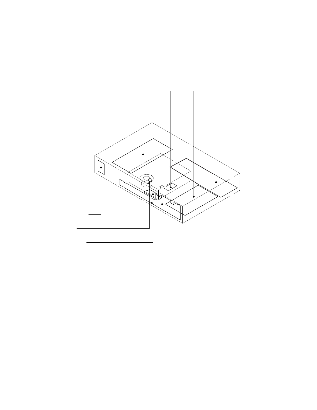
2. LOCATION OF MAIN PARTS AND MECHANISM PARTS
EU05 Output PC board
Feed motor PC board
EU03 Front display PC board
Loading motor PC board
Disc motor PC board
EU04 Power SW PC board
EU01 Main PC board
EU02 Power supply PC board
2-1. Location of Main Parts
Fig. 1-2-1
1-2
Page 7

2-2. Location of Mechanism Parts
y
y
r
d
s
Tr a
Clamper sta
Fig. 1-2-2 Mechanism chassis assembly (Top side)
Loading moto
PC boar
Mechanism chassi
Fig. 1-2-3 Mechanism chassis assembly (Bottom side)
1-3
Page 8

Loading belt
r
r
r
r
Gea
Kick lever
Loading motor
Disc motor
Gea
Gea
Cam Slide
Fig. 1-2-4 Mechanism chassis assembly (Internal side)
1-4
Page 9

Front damper
r
r
y
r
r
d
Gear A
Gear B assembly
Rack gear
assembly
Front dampe
Sub chassis
Pickup assembl
Rear damper
Rear dampe
Fig. 1-2-5 Pickup mechanism chassis assembly (Top side)
Feed moto
Feed moto
PC boar
Fig. 1-2-6 Pickup mechanism chassis assembly (Bottom side)
1-5
Page 10
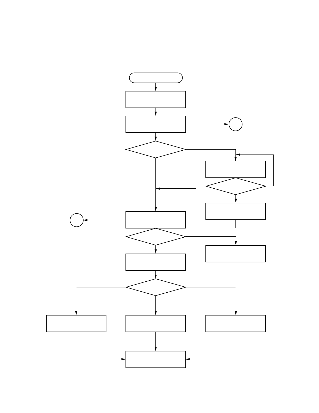
3. TROUBLESHOOTING
3-1. Main Circuit
3-1-1. Servo System
(1) Initial Operation after Power ON
Power ON
Send each LSI hard RST
command and initial command.
Pickup head is positioned at
transmission initial position.
Is tray closed?
Pin 5 of CN502,
TCLS=L
Y
2
NG
Disc presence/absence and
disc judgement
Is a disc present?
Y
DVD or CD initial setting.
N
Tray close operation
Pin 6 of IC601: LDMP = H/L
Pin 7 of IC601: LDMN = L
Tray stops.
Pin 6 of IC601: LDMP = H
Pin 7 of IC601: LDMN = L
N
Laser OFF
Display: INSERT DISC
Monitor screen: NO DISC
1
Is tray closed?
Pin 5 of CN502:
TCLS = L
Y
N
H
DVD single (single-layer)
DVD single
Initial setting.
DVD single
(single-layer)/DVD dual
(dual-layer)/CD?
DVD dual (dual-layer)
DVD dual
Initial setting.
To each disc playback process.
Fig. 1-3-1
1-6
CD
CD
Initial setting.
Page 11

1
Pickup (P.U.) transmission initial
operation does not occur.
The pickup transmission initial operation is carried out to
determine the initial position by transmitting the pickup to the
innermost position once (start-limit switch (pin 4 of CN503)
develops "L".) and to the external direction at low speed
(start-limit switch develops "H", turning off the switch.).
Does pulse of
1.65V 1.65V develop at
pin 162 of IC502?
Y
Check feed gear.
N
Check BUS between IC502
and IC601 and oscillation.
Fig. 1-3-2
2-1
"No disc" misjudgement display of
N
disc presence.
Does lens move with
UP/DOWN full stroke in
focus direction?
Y
N
3
Does focus search
voltage of 1.65V 0.4V develop
at pin 1 of IC504 (E597)?
Y
Does search signal
output at both edges of focus coil?
(Pins 10 to 13 of CN501)
Y
Check pickup head
and wiring.
Is laser current normal?
Y
Does SBAD signal
develop more than 0.3V?
Y
Check peripheral
circuit of IC601.
N
N
Check IC502.
Check IC505.
Fig. 1-3-3
N
Check IC501.
Lens cleaning.
Replace pickup head.
1-7
Page 12

2-2
3
Disc kind misjudgement
(Initial setting is NG.)
N
Are FE and SBAD
signals for each disc normal?
Check peripheral
circuit of IC601.
Check IC501.
Lens cleaning.
Replace pickup head.
Fig. 1-3-4
Check laser current.
lop 50 mA
Y
Check pins 14, 15
and 16 of IC501
serial bus.
Check peripheral
circuits of IC501,
Q501 and Q502.
Check laser current.
50 mA lop 90 mA
lop = Voltage between
E522 and E523/3.3Ω
Y
Check peripheral circuits
of IC501, Q501 and Q502.
lop 90 mA
Check wiring for
pickup head.
Replace pickup
mechanism.
Fig. 1-3-5
DVD single (single-layer) disc
detection waveform
FE signal
Pin150 (TP504) of IC502
SBAD signal
Pin152 (TP506) of IC502
V : 500 mV/div
H : 2 ms/div
Fig. 1-3-6 Fig. 1-3-7 Fig. 1-3-8
1.65V
DVD dual (dual-layer) disc
detection waveform
V : 500 mV/div
H : 2 ms/div
CD disc
detection waveform
V : 500 mV/div
H : 2 ms/div
1-8
Page 13

(2) Picture appears (PLAY)
PLAY
4
2-1
N
N
Disc motor (D.M.) forced
accelleration (500 ms)
Focus search
Is forcus servo
CLV servo ON.
Tracking balance adjustment
Tracking servo ON.
Focus gain adjustment
Tracking gain adjustment
Y
Y
Y
Y
Y
ON?
Repeat three times.
N
N
N
:
Automatic adjustment is carried
out when a disc is replaced after
power ON.
5
4
6
Focus balance adjustment
RF gain adjustment
N
N
Does NG continue
more than 3 s.?
Y
Disc playback NG
Is address code
possible to read?
Y
Search Picture appears.
Fig. 1-3-9
1-9
Page 14

4
Disc motor (D.M.) does not rotate.
Do signals output to
pins 4 to 9 of CN501?
Y
Check IC501.
Does pin 117 of IC502
(TP511) PLCK oscillate around
10 MHz ?
Check peripheral circuits
of IC510 and IC503.
Check disc motor and wiring.
5
Focus servo is NG.
N
N
Are FE, SBAD,
FSON signals normal?
Y
Check peripheral circuit of IC601.
Check wiring for
pickup head.
Lens cleaning.
Replace pickup
mechanism.
Y
Fig. 1-3-10
N
Check peripheral
circuit of IC503.
Focus servo ON
signal waveform
Focus search Focus servo on
Fig. 1-3-12
FE signal
Pin 150 (TP504)
of IC502
0.3V
1.65V
0.3V
SBAD signal
Pin 152 (TP506)
of IC502
Fig. 1-3-11
1-10
Page 15

6
Tracking servo is NG.
Signal waveform at
tracking servo ON (CD)
N
Check IC501.
Fig. 1-3-13
TE signal
Pin 151 (TP503) of IC502
1.65V
RFRP signal
Pin 153 (TP501) of IC502
Is TE signal normal?
Y
Check peripheral
circuit of IC601.
Signal waveform at
tracking servo ON (DVD)
ON search Tracking servo on
Fig. 1-3-14
Search ON (SRCH)
Pin 38 (TP508) of IC502
Fig. 1-3-15
1-11
Page 16

7
Disc playback is NG (DVD).
Is PLL locked?
(Refer to waveforms.)
Y
Check signal process
system following to IC503.
N
Check peripheral circuits of
IC502 and IC601.
N
Check peripheral circuits
of IC501and IC502.
Fig. 1-3-16
Does pulse of
L = 1.65V and H = 3.3V
develop at pin 131 and
L = 0V and H = 1.65V
develop at pin 132
of IC502?
Y
Does RF output
higher than 1.5 V(p-p)
develop at pin 45 (TP515)
of IC501 ?
Y
Pin 57 of IC501 = 2.4V
Pin 58 of IC501 = 3.0V
Y
N
Check peripheral circuits
of IC502 and IC601.
N
Check IC501.
Lens cleaning.
Pickup mechanism
replacement
DVD RF signal
CD RF signal
Fig. 1-3-17
DVD RF signal
Pin 45 (TP515) of IC501
V : 500 mV/div
H : 50 ns/div
CD RF signal
Pin 45 (TP515) of IC501
PLL works as a servo loop to generate a clock signal for reading
RF signal binary data. With the PLL locked, the eye pattern is
identified clearly when triggered with the read clock PLCK.
DVD playback waveform
DVD RF signal
Pin 45 (TP515) of IC501
DVD PLCK
Pin 117 (TP511) of IC502
CH1 : TP515 DVDRF 500 mV/div
CH2 : TP511 DVDPLCK 5 V/div
50 ns/div
Fig. 1-3-19
CD playback waveform
CD RF signal
Pin 45 (TP515) of IC501
Fig. 1-3-18
V : 500 mV/div
H : 100 ns/div
1-12
CH1 : TP515 CDRF 500 mV/div
CH2 : TP511 CDPLCK 5 V/div
100 ns/div
Fig. 1-3-20
CD PLCK
Pin 117 (TP511) of IC502
Page 17

3-1-2. Location Diagram of Servo Test Point
E594 DMDRV
E595 FMDRV
E596 TRDRV
E597 FODRV
CN503
CN502
CN602
E523
E522
TP515 RF
IC504
IC501
IC601
TP506 RFSB
(SBAD)
IC502
CN501
TP503 TE
IC502
CN801
CN901
IC305
CN301
TP505 VREF
TP504 FE
TP501 RFRP
TP511 PLCK
TP507 FSON
TP509 VMCK
(23MHz)
TP508 SRCH
Fig. 1-3-21
1-13
Page 18

This page is not printed.
1-14
Page 19
SECTION 2
PART REPLACEMENT AND
ADJUSTMENT PROCEDURES
CAUTIONS BEFORE STARTING SERVICING
Electronic parts are susceptible to static electricity and may easily damaged, so do not forget to take a proper ground-
ing treatment as required.
Many screws are used inside the unit. To prevent missing, dropping, etc. of the screws, always use a magnetized
screwdriver in servicing. Several kinds of screws are used and some of them need special cautions. That is, take care
of the tapping screws securing molded parts and fine pitch screws used to secure metal parts. If they are used improp-
erly, the screw holes will be easily damaged and the parts can not be fixed.
1. REPLACEMENT OF MECHANICAL PARTS
1-1. Cabinet Replacement
1-1-1. Top Cover
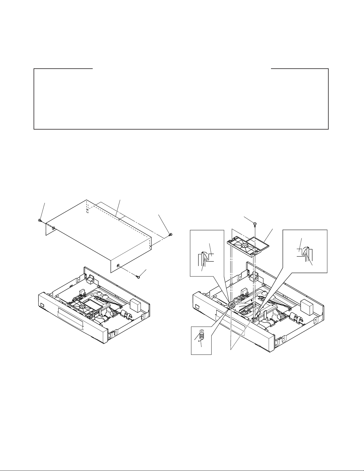
1. Remove five screws (1) and remove the top cover (2).
Screw (1)
Top cover (2)
Screws (1)
Screw (1)
1-1-2. Clamper Stay
<Removal>
1. Remove two screws (1).
2. Release two claws and remove the clamper stay (2).
Screws (1)
Clamper stay (2)
Clamper
stay (2)
Claw
A
Clamper stay (2)
Claw
Fig. 2-1-1
2-1
Spring
Claws
Fig. 2-1-2
Page 20

<Mounting >
1. The spring for tray side pressure is inserted into the
portion “A”. (Refer to Fig. 2-1-2.)
2. By referring to Fig. 2-1-3, insert the spring normally
and mount the clamper stay.
This part should be touch
to the left side of the tray.
NG
1-1-3. Tray Panel
<Tray Ejection>
1. Slide the slider (2) of the mechanism chassis assem-
bly (1) with a screwdriver, etc. in the arrow direction,
so that the tray (3) is ejected.
Note:
• Take care not to damage the pickup and other parts.
OK
Mechanism
chassis assembly
Press down by finger
unitil fix the clamper assembly
NG
Spring
Tray
Screw
driver
Mechanism
chassis assembly (1)
Slider (2)
Tray (3)
Front panel
Fig. 2-1-4
No floating
OK
Fig. 2-1-3
Floating NG
NG
<Tray Panel Removal>
1. Eject the tray (3).
2. Twist the tray panel (4) a little in the arrow A
direction with the tray (3) hold by hand to release
two claws and lift up the tray panel (4) in the arrow B
direction, then the tray panel (4) is removed.
(Refer to Fig. 2-1-5.)
3. When mounting the tray panel (4), insert the tray
panel (4) along the grooves of the both sides of the
tray (3) until clicking.
2-2
Page 21

B
Tray (3)
• After inserting the tray (3), confirm that the mark of
the gear (4) matches with that of the rack gear on the
tray (first tooth of the gear). (Refer to Fig. B.)
Figure A
Gear (4)
Triangle mark
Tray panel (4)
Tray (3)
A
Claws
Tray panel (4)
Fig. 2-1-5
1-1-4. Front Panel and Tray
1. Remove the flexible cable (1).
2. Release four claws and remove the front panel (2).
3. Pull out the tray (3) to this side.
The first tooth of the gear of
this side on the tray rack gear.
Rack gear
Position of the line
Pickup mechanism
assembly
Gear (4)
Slider
Tray (3)
Gear (4)
Claw
Tray (3)
Claws
Front panel (2)
Flexible cable (1)
Claw
Fig. 2-1-6
Note:
• Insert the tray (3) with the front side of the pickup
mechanism assembly descended. (The slider positions to the left side.)
• The gears are required to match their phases each
other. After setting the gear (4) as shown in the figure
“A”, insert the tray (3). When inserting a tray (3),
push the rack gear side shown by the arrow.
Marking
Figure B
Fig. 2-1-7
1-1-5. Rear Panel
1. Remove three screws (1) and remove the rear panel (2).
Screw (1)
Rear panel (2)
Fig. 2-1-8
2-3
Page 22

Tape (3)
Connector (2)
Screws (4)
Screws (5)
Flexible cables (1)
Output
PC board (6)
Twist more than 9 times.
1-2. PC Board Replacement
1-2-1. Main PC Board
Note:
• Before removing the main PC board (4), be sure to
short-circuit the laser diode output land.
After replacing, open the land as it was after inserting
the flexible cables (1).
1. Remove the top cover. (Refer to item 1-1-1.)
2. Remove six flexible cables (1) and remove one
connector (3).
3. Remove four screws (2).
4. Release two claws and remove the main PC board (4).
Note:
• When mounting, be sure to twist the wire for the
connector (3) several times.
Pickup head
1-2-2. Output PC Board
1. Remove the rear panel. (Refer to item 1-1-4
2. Peel off the tape (1).
3. Remove the connector (2).
4. Disconnect two flexible cables (3).
5 Remove the wire part of the connector (5) from the
binding band (4).
6. Remove three screws (6) and remove the output PC
board (7).
Note:
• When mounting, keep the wire part of the connector
(5) with the banding band (4).
Output PC board (7)
Tape (1)
Binding band (4)
Screws (6)
Laser diode
output land
Flexible
cables (1)
Main PC board (4)
Claws
Connector (2)
Screws (2)
Connector (3)
Flexible
cables (1)
Flexible cables (3)
Connector (5)
Fig. 2-1-10
Twist more than 7 times.
Fig. 2-1-9
2-4
Page 23

1-2-3. Power PC board
1. Peel off the tape (1).
2. Remove the connectors (2) and (3).
3. Release the wire part of the connector with the
binding band (4) tightened.
4. Remove three screws (5).
5. Remove two screws (6).
6. Release two claws and remove the power supply PC
board (7).
Power PC board (7)
1-2-4. Front PC Board
1. Remove the front panel. (Refer to item 1-1-4.)
2. Remove four screws (1) and remove the front display
PC board (2)
3. Remove two screws (3) and remove the power switch
PC board (4).
Power SW
PC board (4)
Screws (3)
Front display
PC board (2)
Screws (1)
Screws (5)
Claws
Connector (2)
Tape (1)
Screws (6)
Connector (3)
Fig. 2-1-12
Binding band (4)
Fig. 2-1-11
2-5
Page 24

1-3. Mechanism Parts
1-3-1. Mechanism Chassis Assembly
Note:
• When removing the mechanism chassis assembly (3),
be sure to short-circuit the laser diode output land
before removing the connector and the flexible
cables.
After replacing, open the land as it was after inserting
the connector and flexible cables.
1. Remove the tray. (Refer to items 1-1-3 and 1-1-4.)
2. Remove three flexible cables (1).
3. Remove four screws (2) and remove the mechanism
chassis assembly (3).
1-3-2. Loading Belt
1. Remove the gear (1) by releasing the claw.
2. Remove the gear (2).
3. Remove the gear (3) and the loading belt (4).
4. Replace the loading belt (4) with a new one.
5. When mounting, perform the reverse order of the
removal.
Note:
• When mounting the loading belt (4), twisting and
attaching of a grease, etc. are not allowed.
Gear (1)
Gear (2)
Mechanism
chassis assembly (3)
Screws (2)
Pickup head
Laser diode
output land
Flexible cables (1)
Loading belt (4)
Gear (3)
Claw
Mechanism
chassis assembly
Fig. 2-1-14
Fig. 2-1-13
2-6
Page 25

1-3-3. Loading Motor
1. Remove the loading belt. (Refer to item 1-3-2.)
2. Remove two screws (1) and two claws. Then remove
the loading motor (2) (with the loading motor PC
board (3) attached).
3. Desolder the terminal section of the loading motor (2)
and remove the loading motor PC board (3).
4. Replace the loading motor (2) with a new one.
5. When mounting, perform the reverse order of the
removal.
Note:
• When replacing the loading motor, meet the polarity
phase of the terminals. (Mount the motor with the
label positioned as shown in Fig. 2-1-15.)
1-3-4. Sub Chassis (with a pickup mechanism)
1. Turn the mechanism chassis assembly (1) upside down.
2. Remove one screw (2) and release the boss “A” from the
claw. Then remove the sub chassis (3) (with the pickup
mechanism) by sliding in the arrow direction.
3. When mounting, perform the reverse order of the
removal.
Note:
• When mounting the sub chassis (3) (with the pickup
mechanism), first, insert the boss “C” along the
groove of the cam slider up/down cam (4) and next,
the boss “B” and “A”.
• The boss “A” and “B” may be used with washers.
(One or two washers are used to prevent from the slust
rattling. In some cases, no washer is used.)
When the washer(s) is used, be sure to assemble as it
was without losing.
Mechanism
chassis assembly
Claw
Loading motor (2)
Desolder
Fig. 2-1-15
Screws (1)
Claw
Motor label
side
Loading motor
PC board (3)
Screw (2)
Claw
Sub chassis (3)
(with the pickup mechanism attached)
Boss A
Washers
Boss A
Boss C
Boss B
Groove
Groove
Cam slider
up/down cam (4)
Mechanism chassis
assembly (1)
2-7
Claw
Boss B
Groove
Fig. 2-1-16
Page 26

1-3-5. Pickup Mechanism Assembly
<Removal>
1. Remove four screws (1) and four washers (2) and
then remove the pickup mechanism assembly (3).
<Mounting>
1. Replace the pickup mechanism assembly (3) with a
new one.
2. When mounting, perform the reverse order of the
removal.
Screw (1)
Washers (2)
Damper
(Black)
Damper
(Blue)
Damper
(Black)
1-3-6. Gear B Assembly, Gear A and Rack Gear
Assembly
<Removal>
1. Remove one screw (5) and remove the gear B assem-
bly (1).
2. Remove the gear A (2).
3. Remove one screw (3) and remove the rack gear
assembly (4).
Screw (3)
Gear B assembly (1)
Rack gear
assembly (4)
Gear A (2)
Screw (5)
Claw
Damper
(Blue)
Pickup mechanism
assembly (3)
Fig. 2-1-17
Note:
• The dampers’ color differs when used for the front
side and the rear.
• When mounting the pickup mechanism assembly (2)
with the screws (1), push the pickup mechanism
assembly (2) downward without being caught and
tighten the screws (1) after placing the washer with
the damper bent.
Screw (1)
Washer (2)
Pickup mechanism
assembly (3)
(W6.6P0.5D12)
Pickup mechanism
assembly
Fig. 2-1-19
<Mounting>
1. When mounting, perform the reverse order of the
removal.
2. Mount the gear B assembly (1) by pushing the pickup
head (5) to the disc motor side (arrow A direction)
and shifting the upper gear of the rack gear assembly
(4) in the arrow B direction. (Refer to Fig. 2-1-20.)
3. Fit the positioning holes on the upper gear and lower
gear of the gear B assembly (1) and mount on the
pickup mechanism assembly with the phase matched.
At this time, note that the phase of the gear B
assembly (1) and the gear A (2) shows the status in
the Fig. 2-1-21.
Damper
Fig. 2-1-18
2-8
Page 27

Positioning holes
Gear B assembly (1)
Pickup Head (5)
A
B
Gear A (2)
Pickup mechanism
assembly
Rack gear assembly (4)
Fig. 2-1-20
Note:
• Mount the gear B assembly (1) and the gear A (2)
with their gear teeth placed more than one tooth at
least inside the shaded portion.
Innermost position
of pickup head
Within the position shown
by the shaded porition.
1-3-7. Feed Motor
<Removal>
1. Remove the gear B assembly (1) and the gear A (2).
(Refer to item 1-3-6.)
2. Remove two screws (1) and remove the feed motor (2)
(with the feed motor PC board (3) attached).
(Refer to Fig. 2-1-22.)
3. Desolder the terminals of the feed motor (2) and
remove the feed motor PC board (3).
<Mounting>
1. Tighten the feed motor (2) on the pickup mechanism
assembly with two screws (1).
2. Insert the feed motor PC board (3) with the position-
ing pin on the chassis matched and solder the
terminals.
3. Perform the reverse order of the removal.
Note:
• After mounting, put the lead wires through the notch
of the pickup mechanism assembly.
• When replacing the loading motor, meet the polarity
phase of the terminals. (Mount the motor with the
label positioned as shown in Fig. 2-1-22.)
Screws (1)
Rack gear assembly (4)
Gear A (2)
Fig. 2-1-21
Gear B assembly (1)
Pickup mechanism
assembly
Notch
Lead wires
Feed motor (2)
Motor label
side
Desolder
Feed motor
PC board (3)
Fig. 2-1-22
2-9
Page 28

This page is not printed.
2-10
Page 29

SECTION 3
SERVICING DIAGRAMS
1. STANDING PC BOARDS FOR SERVICING
EU02 Power supply PC board
EU04 Power SW PC board
EU05 Output PC board
EU03 Front display PC board
EU01 Main PC board
Fig. 3-1-1
3-1
Page 30

2. CIRCUIT SYMBOLS AND SUPPLEMENTARY EXPLANATION
100k
Rated Wattage Type Tolerance
100µ
Temperature
response
Rated
voltage
Tolerance
2-1. Precautions for Part Replacement
• In the schematic diagram, parts marked (ex.
F801) are critical part to meet the safety regulations,
so always use the parts bearing specified part codes
(SN) when replacing them.
2-2. Solid Resistor Indication
Unit None ...........Ω
K ...........kΩ
M ...........MΩ
Tolerance None ...........±5%
B ........... ±0.1%
C ........... ±0.25%
D ...........±0.5%
F ...........±1%
G ...........±2%
K ...........±10%
M ...........±20%
Rated Wattage (1) Chip Parts
None ......... 1/16W
(2) Other Parts
None ......... 1/6W
Other than above, described in the Circuit Diagram.
Type None ...........Carbon film
S ...........Solid
R ........... Oxide metal film
W ...........Metal film
W ...........Cement
FR ...........Fusible
• Using the parts other than those specified shall violate
the regulations, and may cause troubles such as
operation failures, fire etc.
Eg. 1
FIg. 3-2-1
2-3. Capacitance Indication
Symbol
Unit None ...........F
Rated voltage None ...........50V
Tolerance (1) Ceramic, plastic, and film capacitors of which
Temperature characteristic None ...........SL
(Ceramic capacitor) For others, temperature characteristics are
Static electricity capacity Sometimes described with abbreviated letters as
(Ceramic capacitor) shown in Eg. 3.
+
...........Electrolytic, Special electrolytic
NP
...........Non polarity electrolytic
...........Ceramic, plastic
M
...........Film
...........Trimmer
µ ...........µF
p ........... pF
For other than 50V and electrolytic capacitors,
described in the Circuit Diagram.
capacitance are more than 10 pF.
None ...........±5% or more
B ........... ±0.1%
C ........... ±0.25%
D ...........±0.5%
F ...........±1%
G ...........±2%
(2) Ceramic, plastic, and film capacitors of which
capacitance are 10 pF or less.
None ...........more than ±5% pF
B ........... ±0.1 pF
C ........... ±0.25 pF
(3) Electrolytic, Trimmer
Tolerance is not described.
described. (For capacitors of 0.01 µF and
no indications are described as F.)
Eg. 2
Fig. 3-2-2
Eg. 3
104
4
pF (0.1µF)
10x10
Temperature characteristic
(or Temperature characteristic+
Static electricity capacity tolerance)
Fig. 3-2-3
3-2
Page 31

2-4. Inductor Indication
10µ
Type Tolerance
Unit None ...........Η
µ ...........µH
m ...........mH
Tolerance None ...........±5%
B ........... ±0.1%
C ........... ±0.25%
D ...........±0.5%
F ...........±1%
G ...........±2%
K ...........±10%
M ...........±20%
2-5. Waveform and Voltage Measurement
• The waveforms for CD/DVD and RF shown in the
circuit diagrams are obtained when a test disc is
played back.
• All voltage values except the waveforms are expressed
in DC and measured by a digital voltmeter.
Eg. 4
Type name
Fig. 3-2-4
Eg. 5
Fig. 3-2-5
3-3
Page 32

2-6. When Replaced ROM ICs or Upgraded Firmware
1. When replaced the following ROM ICs, it is necessary
to write the data into the new ICs.
1) IC615 (firmware)
2) IC613 (Setup default data and other information)
2. When the firmware is upgraded, rewriting the new
firmware into IC615 may be requested for servicing.
DATA UPDATE KIT
(RS-232C Interface/cable)
RS-232C
cable
3. Connect a computer to the main PC board of the DVD
video player with using DATA UPDATE KIT (P/No.
79080074). (Fig. 3-2-6)
4. Writing operation
Refer to the instruction attached to the data floppy
disc.
Computer
(MS-DOS/PC-DOS)
Fig. 3-2-6
Note:
• The firmware and setup data floppy discs are not available as service parts.
CN601
3-4
Page 33

7
6
5
4
3
2
1
VCC+5V
GND
NC
VEE-9V
GND
E+6V
VCC+9V
ANALOG 5V
GND
-5V
-9V
GND
NON REG+6V
ON-OFF 9V
7
6
5
4
3
2
1
1
2
3
4
5
6
7
8
9
10
11
12
13
14
15
16
17
18
19
20
21
22
23
24
25
GND
DA3CSX
DA2CSX
SCLK
SD ATA
AD ATA1
AD ATA3
BCK
LRCK
MCK
MIC ON
ZEROX
X2fs
4448X
G+6dB
RSTX
2131X
MIC-DATA
HMUTE
BIAS+5V
Rch-IN
AGND
Lch-IN
AGND
IEC958IN
VGND
C
R
-INPUT
VGND
C-INPUT
VGND
C
B
-INPUT
VGND
Y-INPUT
DGND
S1
NTPALX
NC
NC
VGND
C
R
-OUTPUT
VGND
C-OUTPUT
VGND
C
B
-OUTPUT
VGND
Y-OUTPUT
DGND
S1
NTPALX
NC
NC
F-
F+
VKK-24V
GND
DSTBX
DSPCKX
DSPSO
DSPSI
DSPRST
STBYX
E+5V
GND
GND
GND
DA3CSX
DA2CSX
SCLK
SD ATA
AD ATA1
AD ATA3
BCK
LRCK
MCK
MIC ON
ZEROX
X2fs
4448X
G+6dB
RSTX
2131X
MIC-DATA
HMUTE
BIAS+5V
Rch-OUT
AGND
Lch-OUT
AGND
IEC958OUT
1
2
3
4
5
6
7
8
9
10
11
12
13
13
12
11
10
9
8
7
6
5
4
3
2
1
25
24
23
22
21
20
19
18
17
16
15
14
13
12
11
10
9
8
7
6
5
4
3
2
1
18
171615
141312
11
10
987654321
123456789
10
111213
141516
17
18
GND
VREF
VCC
F0
E0
A0
D0
C0
B0
F+
T -T+F -
VCC
GND
LD
MON
VOR
GND
LDMP
TOPN
LDMN
TCLS
TRAY
GND
5V
TXD
CTS
RXD
RTS
GND
5V
TXD
CTS
RXD
RTS
FMN
FMP
GND
LMT
DMN
DMP
VCC
DMFG
123456789
1011121314
E12V
EVER 5V
PO ON-OFF SIG
ANALOG 5V
NON REG +6V
ON-OFF 8V
DIGITAL 5V
DIGITAL 3V
GND
GND
GND
-24V
F2 (-)
F1 (+)
GND
E+5V
POWLED
POWKEY
DC+12V
E+5V
PWON
VCC+5V
VCC+6V
M+8V
VDD+5V
VDD+3V
GND
GND
MGND
VKK-24V
F-
F+
123456789
10
11
12
13
14
8765432
1
1234567
8
65432
1
12345
6
123
4
123
4
1
2
3
4
5
6
7
8
9
10
11
12
13
1
2
3
4
5
6
7
8
9
10
11
12
13
12345
6
12345
6
7P
Press-fit
7P
Press-fit
14P
Press-fit
W501
FFC 1mm 18P
FFC 1.25mm 6P W502
FFC 1mm 8P W503
FFC 1mm 4P
W102
FFC 1mm 13P
W602
FFC 1mm 25P
W901
FFC 1mm 13P
W301
CNY03
Board-in
CN802
Lch +6dB
Lch OUT
Lch 0dB
Rch +6dB
Rch OUT
Rch 0dB
CTL
9V
Lch +6dB
Lch OUT
Lch 0dB
Rch +6dB
Rch OUT
Rch 0dB
CTL
9V
8
7
6
5
4
3
2
1
8
7
6
5
4
3
2
1
WW91
(Sub output circuit is not
provided depending on units.)
CNW91
B88-PH-K-S
PUH
TRY
MOTOR
CN501
CN502
CN503
CN801
CN103 CN102
CN801
Board-in
CNY01 CNX01
CN901 CN301
CN603
CN601
CN602
CN101
EU05 OUTPUT
EU52 SUB OUTPUT
MECHA
EU02
POWER
EU04 POWER-SW
EU03 FRONT
EU01 MAIN
3-5 3-6
3. PRINTED WIRING BOARD AND SCHEMATIC DIAGRAM
Fig. 3-3-1
Page 34

PUH
Display-CPU
TMP47C416F
Display
(FL)
Feed
Motor
Tray
Motor
PUH Driver
Motor Driver
KA3032
2M-DRAM
HY512264JC-50
2M-DRAM
HY512264JC-50
Video Encoder
ADV7170
Decryption,
Video Process,MPEG-2 Decoder
Dolby-Digital Decoder, OSD
ZORAN
MD36710X
16M-S-DRAM
HY57V16160ALTC-10 x2
1chip-SERVO
Data Processor
TC9453F
SPM
LPF&VideoOut
x 4ch
Composit Video
Out
S Video Out
Y,C
B,CR video
Out
Coaxial Digital
Audio Out
22. 5792
MHz
Main-CPU
TMP94CS40AF
8M-FROM
MBM29F800TA-55
EE-PROM
S24C04BFJ-TB
9MHz
CeraOSC
27MHz
Xtal OSC
RF Amp.
TA1293F
Data/Control Bus
DVD AV Data
SP DIF Data
Buffer
TC74HCU04AF
LPF&
Amplifier
Audio Out
SL,SR Analog
Audio Out
Y,C Mixer
&Buffer
Track Buffer
4M-DRAM
MSM514800C-70
TC203G08AF
-0103(Z)
Audio-DAC
Audio-DAC1
ICY01
AD71010
Audio-DAC3
ICY31
AD1854
PCM1727
PCM1727
384fs Audio
Master Clock
SW POWER SUPPLY
FRONT DISPLAY UNIT
MAIN PROCESSOR UNIT AUDIO/VIDEO OUTPUT UNIT
IC501
X501
X601
IC504
IC613
IC614
IC615
IC601
IC503
IC502
IC301
IC101
IC306
IC305,302
IC202
IC201
IC901
ICY09
LPF&
Amplifier
Audio Out
FL,FR Analog
Audio out
LPF&
Amplifier
Audio Out
Center SW
Analog
Audio Out
FL2,FR2 Analog
Audio Out
TOS Link Digital
Audio Out
4-1. Overall Block Diagram
4. BLOCK DIAGRAMS
REDUCTION
NOISE
3D
TC209C08HS
2M-FIFO
MSM51V8221A
IC309
IC310
3-83-7
Fig.3-4-1
Page 35

4-2. Power Supply Block Diagram
3-9
Fig. 3-4-2
Page 36

4-3. Front Display, Power Switch Block Diagram
4-3-1. Front Display
4-3-2. Front Display Pattern
Fig. 3-4-3
3-10
Fig. 3-4-4
Page 37

3-11 3-12
4-3-3. Front Display, Power Switch Block Diagram
GP1U263X
BF
Fig. 3-4-5
Page 38

@
7(%&
(4%&
'3'&
)(%&
+)0RG
021
/'
925
'&$
%
9FF
(
)
/' '59
9U$9
)RFXV
&RLO
7UDFNLQJ
&RLO
9GG
9
,& 5)$
,& 5)$
0
0
3
3
7
7
$
$
)
)
(4%
5)*DLQ
)*DLQ
)($03
)(*DLQ
5)(4
5)53
‘ob
/9/'HW
5)$'6%$'
'3'7(DPS
%7(DPS
7(*DLQ
7*DLQ
9UHI &LUFXLW
7(%
7(2
/9/
)(2
5)2
9U'9
9U$
)(%
6HULDO %86 ,)
G%
G%
$
^
'
'LJLWDO HTXDOL]HU
$XWRPDWLF
DGMXVWPHQW
520
5$0
'DWD
VOLFHU
'9' 6\QFKURQRXV
'HWHFWLRQ3URWHFWLRQ
&' 6\QFKURQRXV
'HWHFWLRQ3URWHFWLRQ
GHFRGH
()0 GHFRGH
(&&
(UURU
&RUUHFWLRQ
&RGH
,&
0 '5$0
9&2
3//
70$;
$GGUHVV
&LUFXLW
6HDUFK FRQWURO
˚
FRQ %86 ,)
&''9' 'DWD ,)
&/9 VHUYR
'
^
$
6\VWHP FORFN
9&2
,&
0 '5$0
W
W
R
R
$
$
9
9
SURF
SURF
H
H
VVRU
VVRU
/6
/6
,
,
,&
5)53
,&
,&
7
7
UDFN EXIIHU FRQWUR
UDFN EXIIHU FRQWUR
O
O
@
@@@@@@@@@@@@@
5)&'
5)'9'
)(,
5)6%
7(,
5)53
3:0
'02
)02
'3'%
@
)&6(55
6%$''
@@@@@@@@@@
@@@ @
,&
,&
0$
0$
,
,
1&
1&
3
3
8
8
&RQWURO %86
6(592 6<67(0
6WDQGDUG YROWDJH
/(9(/ 6+,)7
6:
9UU9
9U'9
@
@@@@@@@@@@@@@@@
)FRLO
)FRLO
7FRLO
7FRLO
)03
/(9(/ 6+,)7
/(9(/ 6+,)7
/(9(/ 6+,)7
/(9(/ 6+,)7
)01
'03
'01
&1
&1
&1
)0
'0
6/7 6:
)*
/0
/'03
/'01
7231 6:
7&/6 6:
)2GUY
75GUY
)0GUY
'0GUY
)22
752
/'3
/'1
7231
7&/6
38+20(6/7 6:
'0)*
7UDFN EXIIHU FRQWURO
'HVFUDPEOH
&' 6XEFRGH4 GHFRGH
9&' +HDGHU GHFRGH
,&
,&
6HUYR
6HUYR
^
'DWD SU
'DWD SU
R
R
F
F
H
H
V
V
VR
VR
U
U
7&
7&
)
)
,& 0RWR
,& 0RWR
U
U
'ULYH
'ULYH
U
U
,&.$
,&.$
3/&.
&''9' 'DWD
3-13 3-14
4-4. Main Block Diagrams
4-4-1. Servo System Block Diagram
Fig.3-4-6
Page 39

4-4-2. Logical System Block Diagram
3-163-15
Fig. 3-4-7
Page 40

3-17
1 Q803
AC120V 60Hz input
ON MODE
V:100 V/div
H:5 µs/div
C-3
1 2
4-5. Output Block Diagram
Fig. 3-4-8
5-1. Power Supply Circuit Diagram
5. CIRCUIT DIAGRAMS
3-18
Fig. 3-5-1
Page 41

3-203-19
Fig. 3-5-2
Page 42

3-21 3-22
5-2. Front Display, Power Switch Circuit Diagram
FWY620-1
Fig. 3-5-3
RN2402
220
FWY620-2
10K
Page 43

IC101, Pin
1
IC101, Pin
2
IC101, Pin
3
IC101, Pin
4
14
X-OUT
V: 2 V/div
H: 100 ns/div
22
STB G1
V: 2 V/div
H: 5 ms/div
21
SI
V: 2 V/div
H: 5 ms/div
20
SO
V: 2 V/div
H: 5 ms/div
E-5
E-6
E-6
E-6
IC101, Pin
5
IC101, Pin
6
IC101, Pin
7
19
SCK
V: 2 V/div
H: 5 ms/div
49
V: 10 V/div
H: 5 ms/div
50
S1
V: 10 V/div
H: 5 ms/div
E-6
C-6
C-6
Fig. 3-5-4
Part Loca No. tion
A101 B 2
C101 E 6
C102 D6
C103 F6
C104 F6
CN101 F1
CN102 F7
CN103 F8
D101 F5
D102 D 3
D141 F9
E002 F 3
E004 E 5
E005 E 5
E006 E 5
E007 E 5
E008 E 5
E025 D 6
E026 D 6
E027 D 6
E028 D 6
E029 D 6
E030 D 6
E031 D 6
E032 D 6
E036 D 6
E037 D 6
E038 D 6
E071 D 4
E072 D 4
E073 D 4
E074 D 4
E075 D 4
E076 D 4
E077 D 4
E078 D 4
E080 D 4
E101 F 1
E102 F 1
E103 F 1
E104 F 1
E105 F 1
E106 F 1
E107 F 1
E108 F 1
E109 F 1
E110 F 1
E111 G 1
E113 F 7
E114 F 7
E121 E 3
E122 F 3
E123 D 3
E124 E 6
E125 E 4
E126 F 2
E127 F 2
E128 F 2
E129 F 2
E130 F 2
E131 F 2
E132 C 2
E133 C 3
E134 C 6
E135 E 6
E141 F 8
E142 F 8
E143 F 8
E144 F 8
E145 F10
E146 F 9
E147 F10
E148 F10
EF+1 B 6
EG01 B 3
EG02 B 3
Part Loca No. tion
EG03 B 3
EG04 B 3
EG05 B 3
EG06 B 4
EG07 B 4
EG08 B 4
EG09 B 4
EG10 B 4
EG11 B 4
EG12 B 4
EG13 B 4
EP01 B5
EP02 B5
EP03 B5
EP04 B5
EP05 B5
EP06 B5
EP07 B5
EP08 B5
EP09 B5
EP10 B5
EP11 B5
EP12 B5
EP13 B4
EP14 B4
EP15 B4
EP16 B4
FG101 G2
FG102 G7
IC101 D 5
L101 F6
MT101 E6
Q101 D 6
Q141 F 10
Q142 F 9
R101 F2
R102 F2
R103 F2
R105 F2
R106 F2
R107 F2
R108 F2
R109 F2
R110 F2
R112 F7
R113 F7
R114 G7
R115 E 3
R119 E 2
R120 E 2
R121 F6
R122 F2
R123 E 6
R124 E 6
R125 D6
R126 C6
R128 B7
R129 B7
R130 B7
R131 E 5
R135 F4
R141 F10
R142 F10
R143 F10
R144 F9
R145 F9
R146 F10
S101 E 3
S102 E 3
S103 D 3
S104 D 3
S105 D 3
S106 E 3
S141 F8
SP101 F4
X101 F 5
3-23
Page 44

5-3. Main Circuit Diagrams
5-3-1. Main ICs Information
TC9453F
MD36710X, TMP94CS40AF
TC203G08AF
ADV7170
MBM29F800TA-55
PCM1727
TA1293F
KA3032
S24C01AFJ-TB
3-24
Page 45

Main ICs Function
Table 3-5-1
Ref. No.
IC613
IC306
IC301
IC502
IC501
IC504
IC901
IC601
IC201
IC615
IC309
Pin
No.
1
2
3
4
5
6
7
8
9
10
11
12
13
14
15
16
17
18
19
20
21
22
23
24
25
S24C01AFJ-TB
ADV7170
MD36710X
TC9453F
TA1293F
KA3032
PCM1727
TMP94CS40AF-0103(Z)
TC203G08AF
MBM29F800TA-55
TC203G08AF-0101(Z)
Table 3-5-2 (1/2) ADV7170 Table 3-5-2 (2/2) ADV7170
Name
V
AA
P5-P12
GND
V
AA
P13-P15
HSYNC
FIELD/
VSYNC
BLANK
ALSB
GND
V
AA
GND
RESET
SCLOCK
SDATA
COMP
Power supply
8 bit, 4:2:2 Multiplexed Y/Cr/Cb pixel port
(P7-P0) or
16 bit Y/Cr/Cb pixel port (P15-P0).
P0 represents the LSB.
Ground
Power supply
8 bit, 4:2:2 Multiplexed Y/Cr/Cb pixel port
(P7-P0) or
16 bit Y/Cr/Cb pixel port (P15-P0).
P0 represents the LSB.
HSYNC (Modes 1 & 2) control signal.
Master Mode: control signal output
Slave Mode: control signal acceptance
Dual function field (Mode 1) and VSYNC
(mode 2) control signal.
Master Mode: control signal output
Slave Mode: control signal acceptance
Video blanking control signal. The pixel
inputs are ignored when this is logic level
"0". This signal is optional.
TTL address input. This signal set up the
LSB of the MPU address.
Ground pin
Power supply
Ground pin
This pin resets the on-chip timing generator
and sets the ADV7170 into default mode.
NTSC operation, timing slave mode 0, 8 bit
operation, 2 x composite & S VHS OUT.
MPU port serial interface clock input
MPU port serial data input/output
Compensation pin. Connect a 0.1µF
capacitor from COMP to VAA. For
optimum dynamic performance in low
power mode, the value of the COMP
capacitor can be varied as described in
low power mode section.
IC Name
Function
EE-PROM
Video Encorder
AV Decorder
SERVO & Data Processor
RF Signal processing IC
5-CH Motor Driver
DA Converter
Main Micro Processor
Track Buffer
Flash ROM
3D DNR
Function
Detail
Setup default, memorization of specification setting.
Built-in D/A converter. Encodes digital video signal to analog video
signal of NTSC/PAL system.
Decryption, MPEG-2 Decode, Audio Decode, Sub Picture Decode,
OSD.
Performs servo control of DVD or CD, and performs demodulation
and correction of RF signal.
Equalizes of playback RF signal and generates error detection signal
required for each servo operation.
5ch driver for motor driving.
Stereo audio DA converter with a dual PPL built-in.
Performs system control for all circuits.
Rate control and Buffer control.
Memorization for firmware.
3 Dimension Digital Noise Reduction.
Pin
No.
26
Name
RED/
RED/S-VHS C/V analog output.
Function
CHROMA/V
27
GREEN/
Green/S-VHS Y/Y analog output.
LUMA/Y
28
29
30
31
V
AA
GND
V
AA
BLUE/
Power supply
Ground pin
Power supply
Blue/Composite/U analog output
CVBS/U
32
COMPO-
PAL/NTSC composite video output.
SITE
(CVBS)
33
34
V
R
REF
SET
Voltage reference input for DACs or
voltage reference output.
A 150 ohm resistor connected from this
pin to GND is used to control full scale
amplitudes of the video signal.
35
SCRESET/
RTC
This pin can be configured as an input by
setting MR22 and MR21 of mode register
2. It can be configured as a subcarrier
reset pin, in which case a high to low
transition on this pin will reset the
subcarrier to field 0. Alternately it may be
configured as a real time control (RTC)
input.
36
TTX REQ
Teletext data request signal
Defaults to GND when teletext not selected
(enables backward compatibility to
ADV7175/ADV7176).
37
TTX V
Teletext data
AA
Defaults to VAA when teletext not selected
(enables backward compatibility to
ADV7175A/ADV7176.)
38
39
40
41
P0-P4
8 bit, 4:2:2 Multiplexed Y/Cr/Cb pixel port
(P7-P0) or
16 bit Y/Cr/Cb pixel port (P15-P0). P0
represents the LSB.
42
43
44
GND
CLOCK
Ground pin
TTL clock input.
3-25
Page 46

Table 3-5-3 KA3032
Table 3-5-4 MBM29F800TA-55
Pin
No.
1
2
3
4
5
6
7
8
9
10
11
12
13
14
15
16
17
18
19
20
21
22
23
24
25
26
27
28
29
30
31
32
33
34
35
36
37
38
39
40
41
42
43
44
45
46
47
48
Name
OUT1
IN2.1
IN2.2
OUT2
IN3.1
GND
IN3.2
OUT3
IN4.1
IN4.2
OUT4
CTL
FWD1
REV1
SGND
OPOUT
GND
OPIN(+)
IPIN(–)
MUTE4
MUTE3
MUTE1,2
PVCC1
DO5.2
DO5.1
DO4.2
DO4.1
GND
DO3.2
DO3.1
PGND
DO2.2
DO2.1
DO1.2
DO1.1
PVCC2
GEG50
REG050
GND
RES50
SVCC
REF
IN1.1
IN1.2
Function
CH1 OP-AMP output
CH2 OP-AMP input (+)
CH2 OP-AMP input (–)
CH2 OP-AMP output
CH3 OP-AMP input (+)
Ground
CH3 OP-AMP input (–)
CH3 OP-AMP output
CH4 OP-AMP input (+)
CH4 OP-AMP input (–)
CH4 OP-AMP output
CH5 motor speed control
CH5 forward input
CH5 reverse input
Signal ground
OP-AMP output
Ground
OP-AMP input (+)
OP-AMP input (–)
CH4 mute
CH3 mute
CH1,2 mute
Power supply voltage (for CH5)
CH5 drive output
CH5 drive output
CH4 drive output
CH4 drive output
Ground
CH3 drive output
CH3 drive output
Power ground
CH2 drive output
CH2 drive output
CH1 drive output
CH1 drive output
Power supply voltage
(for CH1, CH2, CH3, CH4)
Regulator output
Regulator 5V output
Ground
Regulator reset
Signal supply voltage
Bias voltage input
CH1 OP-AMP input (+)
CH1 OP-AMP input (–)
Pin
No.
1
8
16
24
25
45
48
29
36
38
45
26
28
11
12
15
47
27
37
9
10
13
14
|
|
|
|
Name
A–1,
A0 – A
18
DQ0 – DQ
CE
OE
WE
RESET
RY/BY
BYTE
V
SS
V
CC
N.C.
Address input
Data I/O
15
Chip enable
Output enable
Write enable
Hardware reset
Ready/busy output
8 bit, 16 bit mode switch
Ground
Power supply
Not connected.
Function
3-26
Page 47

Table 3-5-5 MD36710X (1/5) Table 3-5-5 MD36710X (2/5)
Pin
No.
Host Interface, CD-DSP interface, Sub ode interface (32 pins)
3
4
5
6
7
9
10
11
12
14
|
16
19
|
21
22
24
25
26
27
29
30
31
32
34
Name
HD [15:12]
CDERR (HD [15])
CDFRM (HD [14])
CDDAT (HD [13])
CDDAT (HD [12])
HD [11:8]
SCCLK (HD [11])
SCDAT (HD [10])
SCSYN (HD [9])
SCFRM (HD [8])
HD [7:0]
HA [3:0]
HWR# (HR/W#)
HCS#
HRD# (HDS#)
HRDY
HACK#
HIRQ#
Function
When connecting HWID to VDD,
become data lines 15:12 of 16 bit host
data bus. When connecting HWID to
GND, the lines become CD-DSP serial
input port pins defined as below.
CD-DSP data error input
CD-DSP LR clock (frame) input
CD-DSP data input
CD-DSP bit clock input
When connecting HWID to VDD,
become data lines 11:8 of 16 bit host
data bus. When connecting HWID to
GND, the lines become sub code port
pins defined as below.
Sub code bit clock output
Sub code bit clock input
Sub code sync signal display input
Sub code frame sync input
8 I.s. host data bus. When connecting
HWID to GND, only the 8 I.s. signal is
defined as a host data signal. When
connecting HWID to VDD, 8 I.s. line is
used for of 16 bit data bus.
Host address input. Inputs address
signal that specifies physical address
inside MD36710X.
Host protocol, type A
(HTYPE=GND): HR/W#. Decides
direction of host access.
Host protocol, type B (HTYPE=VDD):
HWR#. Host writing input (active low).
Host chip select input. Active low.
Host protocol, type A (HTYPE=GND):
HDS#.
Data strobe input (active low).
Host protocol, type B (HTYPE=VDD):
HRD#.
Host writing input (active low).
Host ready output (active high). Use
this signal to transmit bit stream via
host bus. External pull-up resistor is
required.
Transmission of CodBurstLen byte
length is determined as 1 packet.
Check that the signal is active before
transmitting each packet. Possible to
write the bit stream serially up to
CodBurstLen byte to MD36710X.
Host acknowledge output (active low).
Protocol is type A, MD36710X asserts
this output and notify completion of
reading or writing cycle.
If this signal is not active, 3-state
condition occurs (External pull-up
resistor is required.).
If protocol is type B, the signal
functions as wait output signal. When
high speed host (microprocessor) is
used, this signal may not be used.
Interruption requirement (active low).
Deassert when host reads interruption
status resister of MD36710X. Also
deassert after host masks interruption in
the interrupt mask resister of
MD36710X or reseting.
If HIRQ# is not asserted, 3-state
condition occurs (External pull-up
resistor is required.)
Pin
No.
35
36
37
130
141
142
GPI/O signal (4 pins)
2
122
123
159
PLL signal (6 pins)
126
128
129
135
137
136
Name
HWID
HORD
HTYPE
STNDBY#
RESET#
IDLE
GPSI
GPAI/O [1:0]
GPSO
GCLK1
XO
GCLK
PLLCFG [1:0]
PLLCA
Function
Determines data bus width of host
interface. It can be changed only
during reset. Host interface of
MD36710X is set to 8 bit width at low
level (GND) and set to 16 bit width at
high level (VDD).
Determines byte order for data bus of
host interface in 16 bit width setting.
(HWID: VDD).
It can be changed only during reset.
Set MD36710X to obtain I/O signals of
m.s. byte in HD [15:8] at low level
(GND) and those in HD [7:0] at high
level.
If HWID is GND level, connect to
GND.
Determines protocol of host bus. It
can be changed only during reset.
Sets MD36710X to type A at low level
and type B at High level.
Standby input (active low). All output
pins and bidirectional pins become
float state if asserting with RESET#
and MD36710X is cut electrically from
peripheral circuits. All internal
operation stop and power
consumption is confined to the
minimum.
Contents of SDRAM are not stored at
stanby.
Reset input (active low). Initializing
process of MD36710X starts at the
time deasserting is carried out from
assert state.
Idle, init or reset states display output
(active high).
General input controlled by DVP micro
code.
General bidirectional pin controlled by
ADP micro code. After resetting, this
pin is defined as an input pin. ADP
command specifies the setting.
General output conrolled by DVP
micro code.
Master clock input for audio. Must
be connected to GCLK for usual
operation.
Output to the crystal connected to
GCLK. If the crystal is not used for
GCLK, XO is not connected.
Clock for main processor or crystal
input.
PLL configuration input. It can be
changed only during reset. Both pins
must be connected to GND (digital)
for usual operation.
Capacitor connection pin for PLL.
Connect the other terminal of the
capacitor to PLLGND.
3-27
Page 48

Table 3-5-5 MD36710X (3/5) Table 3-5-5 MD36710X (4/5)
Pin
No.
Digital video port (24 pins)
84
85
87
89
90
91
92
94
|
97
99
|
101
98
102
104
105
106
107
109
|
111
124
Digital audio port (8 pins)
112
114
115
116
117
118
119
Name
VCLK
VMASTER
VDEN#
VSYNC
HSYNC
FI
Y [7:0]
CBLANK
C [7:0]
OSDPLT (C [4])
OSDPEL [3:0]
(C [3:0])
VCLKx2
AIN
AOUT [2:0]
S/PDIF
(AOUT [3])
ALRCLK
ABCLK
Function
VCLKx2 signal is divided by 2. Used
as a qualifier of data and sync signal.
Video master/slave selection input. At
high level, video sync in MD36710X
enters master mode. (Video sync and
clock signals are developed.) After
low level, video sync enters slave
mode. (Video sync and clock signals
are entered.)
Only during reset, setting of terminal
can be changed.
Video enable input (active low). When
active, MD 36710X develops video
data. When deasserting, pixel output
becomes 3-state condition. (But sync
and clock signals are kept to be
active.)
Input is changeable at any time but
becomes effective at the next
VCLKx2.
Vertical sync bidirectional signal pin.
Polarity and length are programmable.
Horizontal sync bidirectional signal
pin. Polarity and length are
programmable.
Field identification bidirectional signal
pin. Polarity is programmable.
At 16 bit video mode (Video 8=0),
develop luminance signals. At 8 bit
mode (Video 8=1), develop luminance
and color difference signals
multiplexed in time sequence
according to the ITU-R656 standard
(in no relation to presence of SAV and
EAV sync code).
Composite blank output. Waveforms are
programmable other than polarity.
At 16 bit video mode (Video 8=0),
develop color difference signal. At 8
bit mode (Video 8=1), m.s. line 3 pin
(c [7:5]) is not used, I.s.5 pin (C [4:0])
is used as input from external OSD
device.
On-chip OSD palette selector. Selects
OSD Palette0 at low level and OSD
Plette1 at high level.
OSD pixel input. Used as an entry
signal to on-chip OSD palette.
Main video clock input or output.
Serial input of PCM stereo audio for
ADC
Serial output of PCM stereo audio for
DAC. After reset, develop signals of
low level. Only AOUT [0] supports 24
bit sample width.
S/PDIF transmitter output. Possible to
connected to DAC as the forth audio
output (AOUT [3]). After reset,
develop signal of low level.
LR clock output of AOUT [3..0] and
AIN. Becomes square waveform in
sampling frequency. Polarity of LR is
programmable.
Bit clock output of AOUT [3..0] and
AIN. At rising/falling edges
(programmable) AOUT is developed
and AIN is latched.
Pin
No.
132
DVD-DSP interface (13 pins)
143
144
146
147
148
149
151
|
154
156
|
158
SDRAM interface (35 pins)
38
39
42
|
47
49
|
52
54
55
56
57
59
60
61
62
64
|
67
69
|
72
74
|
79
82
TEST signal (3 pins)
83
127
139
Name
AMCLK
DVDERR
DVDSOS
DVDVALID
DVDSTRB
DVDREQ
DVDDAT [7:0]
RAMADD [11:0]
RAMCS0#
RAMCS1#
RAMRAS#
PCLK
RAMCAS#
RAMWE#
RAMDQM
RAMDAT [15:0]
TESTMODE
SCNENBL
ICEMODE
Audio master clock I/O. 384 fs, 256 fs,
192 fs and 128 fs of sampling
frequency can be selected
(programmable).
DVD-DSP error input (Polarity
programmable)
DVD-DSP data selector start input
(Polarity programmable)
DVD-DSP data effective input
(Polarity programmable)
DVD-DSP data bit strobe (clock)
input. Polarity programmable.
DVD-DSP data requirement output
(Polarity programmable)
DVD-DSP data input bus
SDRAM address bus output
SDRAM chip select (active low)
output. Lower bit for 2 Mbyte device.
SDRAM ship select (active low).
Upper bit for 2 Mbyte device.
Row selection of SDRAM (active low)
output
SDRAM clock output (same as
internal process clock).
Column selection of SDRAM (active
high) output
SDRAM write enable (active low)
output
SDRAM data masking (active high)
output
SDRAM bidirectional data bus
Test pin. Connects to VDD for normal.
Test pin. Connects to GND for normal.
Test pin. Connects to VDD for normal.
Function
3-28
Page 49

Table 3-5-6 PCM1727Table 3-5-5 MD36710X (5/5)
Pin
No.
Name
Power signal (35 pins)
GND
1
40
41
53
68
80
81
93
108
120
121
125
131
145
160
VDD
8
28
33
48
58
63
73
86
78
113
133
140
150
155
PLLGND (GNDA)
134
PLLVDD (VDDA)
138
Function
Digital GND
Digital power supply (3.3V)
GND of internal PLL circuit
Power supply of internal PLL circuit
Pin
No.
1
2
3
4
5
6
7
8
9
10
11
12
13
14
15
16
17
18
19
20
21
22
23
24
Name
XT1
PGND
V
CP
MCKO
RSV
SCKO3
ML
MC
MD
RSTB
V
R
OUT
AGND
V
CA
V
L
OUT
CAP
ZERO
BCK
DATA
LRCK
SCKO2
SCKO1
V
DD
DGND
XT2
Function
PLL master clock input or crystal
connector terminal
PLL GND
PLL power supply
Master clock buffer output
Not connected. Use the pin with open.
PLL-2 generation system clock output.
Serial control data enable input.
Serial control data clock input.
Serial control data, data input.
External reset input, reset at L.
(1)
(1)
(1)
(1)
Rch analog audio output
Analog GND
Analog power supply
Lch analog audio output
Internal analog bias
(connected with a bypass capacitor)
Infinity zero detection output.
PCM audio data, bit clock input.
PCM audio data, data input.
PCM audio data, LRCK input (fs)
(2)
(3)
(3)
(3)
PLL-1 generation system clock output
PLL-1 generation system clock output
Digital power supply
Digital GND
Crystal oscillator connection terminal,
connected to GND at external clock input.
Note:
(1) With internal pull-up. Schmitt trigger input.
(2) Open drain output.
(3) Schmitt trigger input.
Table 3-5-7 S-24C01AFJ-TB-01
Pin
No.
1
2
3
4
5
6
7
8
Name
A0
A1
A2
GND
SDA
SCL
TEST
V
CC
Address input
Address input
Address input
Ground
Serial data I/O
Serial clock input
Connect to GND.
Power supply
Function
3-29
Page 50

Table 3-5-8 (1/2) TA1293F Table 3-5-8 (2/2) TA1293F
Pin
No.
1
2
3
4
5
6
7
8
9
10
11
12
13
14
15
16
17
18
19
20
21
22
23
24
25
26
27
28
29
30
31
32
33
34
35
36
37
38
39
40
41
42
43
44
45
46
47
48
49
50
51
52
53
54
55
Name
GNDP
LDO2
MDI2
NC
VrA
Vrfi
VrD
Vdd
DPAC
DPBD
DPD1
DPD2
SCB
SCL
SCD
VRCK
NC
VCKF
VccP
NC
RFSW
VccS
NC
LV L
NC
TEO
FEO
NC
DFTN
RPZ
RPO
RPB
RPP
RFO
VccR
DPDB
TEB
FEB
PSC
VccO
Vcc2
NC
EQD
GND2
Function
GND terminal
Drive terminal
Monitor terminal
–––
Analog V
Filter capacity for reference
Digital V
Power supply terminal
DPD AC coupling capacity 1
DPD AC coupling capacity 2
DPD integration capacity 1
DPD integration capacity 2
Control line (bit clock)
Control line (latch signal)
Control line (serial data)
Reference clock input
Capacity for time constant adjustment
Power supply terminal
RFO control terminal
Power supply terminal
Servo addition output
TE output
FE output
DPD defect
RF ripple center output
RF ripple output
Bottom of RF ripple
Peak of RF ripple
Equivalent RF output
Power supply terminal (RF)
Pit depth adjustment
TE balance
FE balance
VRCK dividing ON/OFF
Power supply terminal
Power supply terminal
Group delay correction
GND terminal
REF
REF
–––
–––
–––
–––
–––
–––
Pin
No.
56
57
58
59
60
61
62
63
64
65
66
67
68
69
70
71
72
73
74
75
76
77
78
79
80
Name
RFDC
EQB
EQF
MDI1
LDO1
P1TN
P1TP
P1FN
P1FP
LDP1
GNDR
P1DI
P1CI
P1BI
P1AI
LDP2
P2AI
P2BI
P2CI
P2DI
GNDS
P2FP
P2FN
P2TP
P2TN
Function
DC feed back capacity
Boost adjustment
Frequency adjustment
Monitor input
Drive output
TE– input (DVD)
TE+ input (DVD)
FE– input (DVD)
FE+ input (DVD)
APC polarity 1
GND terminal
D input (DVD)
C input (DVD)
B input (DVD)
A input (DVD)
APC polarity 2
A input (CD)
B input (CD)
C input (CD)
D input (CD)
GND terminal
FE+ input (CD)
FE– input (CD)
TE+ input (CD)
TE– input (CD)
3-30
Page 51

Table 3-5-9 (1/4) TC9453F Table 3-5-9 (2/4) TC9453F
Pin
No.
1
2
3
4
5
6
7
8
9
10
11
12
13
14
15
16
17
18
19
20
21
22
23
24
25
26
27
28
29
30
31
32
33
34
35
36
37
38
39
40
41
42
43
44
45
46
47
48
49
50
51
52
53
54
55
56
57
58
Name
NC
DVSS
RO
DVDD
DVR
LO
DVSS
XVSS
XI
XO
XVDD
TESM0
TESM1
TESM2
VDD3
VSS3
VPFC
TEST0
VLPFI
VLPFO
VSS3
MON0
MON1
MON2
MON3
MON4
MON5
MON6
MON7
MON8
MON9
VDD3
NC
TEST1
FLGA
FLGB
VSS3
/RST
/MA
/MRD
/MWR
/MCE
/MINT
MD0
MD1
MD2
MD3
MD4
MD5
MD6
MD7
VDD5
NC
SMCK
VMCK
Function
–––
Exclusive ground for DAC
R-ch output signal
Exclusive power supply for DAC
Amplifier reference signal output
L-ch output signal
Exclusive ground for DAC
Exclusive ground for oscillator
Crystal oscillation input
Crystal oscillation output
Exclusive power supply for oscillator
Test terminal
Digital power supply
Digital ground
Clock PLL phase/frequency comparison
output
Test mode terminal
VCO filter input for clock PLL
VCO filter output for clock PLL
Digital ground
Test monitor
Digital power supply
–––
Test mode terminal
General I/O or flag monitor
General I/O or flag monitor
Digital ground
Reset terminal
Microprocessor address enable signal
Microprocessor data read signal
Microprocessor data write signal
Microprocessor chip enable signal
Microprocessor interrupt signal
Microprocessor data bus
Power supply
–––
Clock output
Data output (signal process) clock output
Pin
No.
59
60
61
62
63
64
65
66
67
68
69
70
71
72
73
74
75
76
77
78
79
80
81
82
83
84
85
86
87
88
89
90
91
92
93
94
95
96
97
98
99
100
101
102
103
104
105
106
107
108
109
110
111
112
113
114
115
116
117
Name
VDD3
PD0
VSS5
PD1
PD2
PD3
PD4
VSS3
PD5
PD6
PD7
PD8
/PSYC
/PDRQ
PDCK
VDD5
TESM3
DIGI
TESM4
VDD3
BA0
BA1
BA2
BA3
VSS5
BA4
BA5
BA6
BA7
BA8
VDD3
/BOE
/BRAS
/BCAS
/BWL
/BWU
VDD5
BD0
BD1
BD2
BD3
BD4
BD5
BD6
BD7
BD8
VSS3
BD9
BD10
BD11
BD12
VSS5
BD13
BD14
BD15
NC
VDD3
PLCK
Function
Digital power supply
DVD/CD data output
Ground
DVD/CD data output
Digital ground
DVD/CD data output
DVD data sector sync signal
DVD data transfer block
DVD data transfer clock
Power supply for 5V
Test terminal
1 bit DAC digital IN input
Test terminal
Digital power supply
External RAM address output
Ground
External RAM address output
Digital power supply
External RAM/OE signal
External RAM/RAS signal
External RAM/CAS signal
External RAM Lower/WE signal
External RAM Upper/WE signal
Power supply
External RAM data I/O
Digital ground
External RAM data I/O
Ground
External RAM data I/O
–––
Digital power supply
PLL clock I/O
3-31
Page 52

Table 3-5-9 (3/4) TC9453F Table 3-5-9 (4/4) TC9453F
Pin
No.
118
119
120
121
122
123
124
125
126
127
128
129
130
131
132
133
134
135
136
137
138
139
140
141
142
143
144
145
146
147
148
149
150
151
152
153
154
155
156
157
158
159
160
161
162
163
Name
TESM5
TESM6
TESM7
TESM8
VSS3
CFC1
CFC2
PPW
PESV
PVSS
PESP
PDOP1
PDON1
PDOP2
PDON2
LPFN
LPFO
PVREF
VCOREF
VCOF
PVDD
SLCO1
TESM9
TEST2
RFCD
RFDVD
AVDD
RFCT
RFZI
TEZI
AWIN
AVSS
FEI
TEI
RFSB
RFRP
AVSS
TESM10
EXTAD
VREF
FOO
TRO
AVDD
AWCTL
FMO
DMO
Function
Test terminal
Digital ground
VCO frequency control signal
VCO frequency control signal
Phase comparator offset adjustment voltage
output
Phase comparator offset adjustment signal
input
Exclusive ground for PLL
Phase comparator offset adjustment signal
output
DVD/CD phase control signal
(Positive polarity)
DVD/CD phase control signal
(Negative polarity)
DVD/CD phase control signal
(Positive polarity)
DVD/CD phase control signal
(Negative polarity)
Data PLL low pass filter inverted input
Data PLL low pass filter output
Exclusive reference power supply for data
PLL
VCO reference
VCO automatic adjustment filter output
Exclusive power supply for PLL
Data slice 6 bit DAC output
Test terminal
Test mode terminal
CD RF signal input
DVD RF signal input
Exclusive power supply for analog
RFRP center voltage input (zero cross)
RFRP signal input (zero cross)
Tracking error signal input (zero cross)
Active wide PLL control signal input
Exclusive ground for analog
Focus error signal input
Tracking error signal input
RF level or sub beam signal addition input
RFRP signal input
Exclusive ground for analog
Test terminal
General external ADC input
Exclusive reference power supply for
analog
Focus EQ output
Tracking EQ output
Exclusive power supply for analog
Active wide PLL control output
Focus EQ output
Disc EQ output
Pin
167
168
169
170
171
172
173
174
175
176
Name
TEBC
FEBC
DPDC
EQBC
ANMON
/DFCT
VRCK
VSS3
SCD
SCL
SCB
FGIN
NC
Tracking balance control signal
Focus balance control signal
DPD error signal pit depth adjustment
signal
RF wide range boost adjustment signal
General PWM output
Black dot detection signal
RF EQ characteristic control clock
Digital ground
Head amplifier serial data
Head amplifier serial data latch pulse
Head amplifier serial data clock
Disc FG signal input (with self-bias circuit)
No.
164
165
166
* “ / ” indicated at the head of pin name means active “L” pin.
Function
–––
3-32
Page 53

Table 3-5-10 (1/5) TMP94CS40AF Table 3-5-10 (2/5) TMP94CS40AF
Pin
No.
77
|
84
86
|
93
95
|
102
104
|
111
113
|
120
122
|
129
131
|
138
75
74
73
72
71
Name
P00 – P07
D0 – D7
P10 – P17
D8 – D15
P20 – P27
D16 – D23
P30 – P37
D24 – D31
P40 – P47
A0 – A7
P50 – P57
A8 – A15
P60 – P67
A16 – A23
P70
RD
P71
WRLL
P72
WRLH
P73
WRHL
P74
WRHH
Function
Port 0: I/O port.
Data 0–7: data bus 0–7.
Function is selectable by setting of AM0/1
terminal.
It becomes high impedance at no external
memory access.
Port 1: I/O port.
Data 8–15: data bus 8–15.
Function is selectable by setting of AM0/1
terminal.
It becomes high impedance at no external
memory access.
Port 2: I/O port.
Data 16–23: data bus 16–23.
Function is selectable by setting of AM0/1
terminal.
It becomes high impedance at no external
memory access.
Port 3: I/O port.
Data 24–31: data bus 24–31.
Function is selectable by setting of AM0/1
terminal.
It becomes high impedance at no external
memory access.
Port 4: I/O port.
Address 0–7: address bus 0–7.
Function is selectable by setting of AM0/1
terminal.
Signal does not change at no external
memory access.
Port 5: I/O port.
Address 8–15: address bus 8–15.
Function is selectable by setting of AM0/1
terminal.
Signal does not change at no external
memory access.
Port 6: I/O port.
Address 16–23: address bus 16–23.
Function is selectable by setting of AM0/1
terminal.
Signal does not change at no external
memory access.
Port 70: output port. (Initializes to “1” output.)
Read: strobe signal reading external memory.
Function is selectable by setting of AM0/1
terminal.
Strobe signal is not developed at no
external memory access.
Port 71: output port. (Initializes to “1” output.)
Write: strobe signal writing D0–D7 of
external memory.
Strobe signal is not developed at no
external memory access.
Port 72: output port. (Initializes to “1” output.)
Write: strobe signal writing D8–D15 of
external memory.
Strobe signal is not developed at no
external memory access.
Port 73: output port. (Initializes to “1” output.)
Write: strobe signal writing D16–D23 of
external memory.
Strobe signal is not developed at no
external memory access.
Port 74: output port. (Initializes to “1” output.)
Write: strobe signal writing D24–D31 of
external memory.
Strobe signal is not developed at no
external memory access.
Pin
No.
70
69
67
66
65
64
63
62
49
60
59
58
57
56
Name
P75
BUSRQ
P76
BUSAK
P80
CS0
P81
CS1
RAS0
P82
CS2
P83
CS3
RAS1
P84
CS4
P85
CS5
P86
WAIT
PA 0
CAS0
LCAS0
PA 1
UCAS0
PA 2
OE0
PA 3
OE1
PA 4
WE0
Function
Port 75: I/O port.
Bus request: signal with memory interface
terminal requested to be high impedance.
The following pins become high
impedance, but no change is made when
used as a port.
A0 – A23, D0 – D31, RD, WRLL, WRLH,
WRHL, WRHH, CS0 – CS5, OE0 – OE1,
WE0–WE1, RAS group, CAS group
Port 75: output port. (Initializes to “1” output.)
Bus acknowledge: signal, that indicates
request of BUSRQ received.
Port 80: output port. (Initializes to “1” output.)
Chip select 0: “L” level is developed if
address is within the assigned address
range.
Port 81: output port. (Initializes to “1” output.)
Chip select 1: “L” level is developed if
address is within the assigned address
range.
Low address strobe 0: RAS strobe signal
for DRAM is developed if address is within
the assigned address range.
Port 82: output port. (Initializes to “0” output.)
Chip select 2: “L” level is developed if
address is within the assigned address
range.
Port 83: output port. (Initializes to “1” output.)
Chip select 3: “L” level is developed if
address is within the assigned address
range.
Low address strobe 1: RAS strobe signal
for DRAM is developed if address is within
the assigned address range.
Port 84: output port. (Initializes to “1” output.)
Chip select 4: “L” level is developed if
address is within the assigned address
range.
Port 85: output port. (Initializes to “1” output.)
Chip select 5: “L” level is developed if
address is within the assigned address
range.
Port 86: I/O port.
Wait: Bus wait request signal
Port A0: output port. (Initializes to “1” output.)
Column address strobe 0: CAS strobe
signal for DRAM is developed if address is
within the assigned address range.
Lower column address strobe 0: lower CAS
strobe signal for DRAM is developed if
address is within the assigned address
range.
Port A1: output port. (Initializes to “1” output.)
Upper column address strobe 0: upper CAS
strobe signal for DRAM is developed if
address is within the assigned address
range.
Port A2: output port. (Initializes to “1” output.)
Out enable 0: out enable signal for DRAM is
developed.
Port A3: output port. (Initializes to “1” output.)
Out enable 1: out enable signal for DRAM is
developed.
Port A4: output port. (Initializes to “1” output.)
Write enable 0: write enable signal for
DRAM is developed.
3-33
Page 54

Table 3-5-10 (3/5) TMP94CS40AF Table 3-5-10 (4/5) TMP94CS40AF
Pin
No.
55
54
53
52
51
140
141
17
18
19
20
21
22
24
25
13
Name
PB0
CAS1
LCAS1
LLCAS1
PB1
UCAS1
LUCAS1
PB2
HLCAS1
PB3
HUCAS1
PB4
WE1
PC0
TO1
TO7
PC1
TO3
TOB
PD0
TO4
PD1
TI4
INT4
PD2
TI5
INT5
PD4
TO6
PD5
TI6
INT6
PD6
TI7
INT7
PE0
TO8
PE1
TI8
INT8
PE2
TI9
INT9
Function
Port B0: output port. (Initializes to “1” output.)
Column address strobe 1: CAS strobe
signal for DRAM is developed if address is
within the assigned address range.
Lower column address strobe 1: lower CAS
strobe signal for DRAM is developed if
address is within the assigned address
range.
Lower-lower column address strobe 1:
lower-lower CAS strobe signal for DRAM is
developed if address is within the assigned
address range.
Port B1: output port. (Initializes to “1” output.)
Upper column address strobe 1: upper CAS
strobe signal for DRAM is developed if
address is within the assigned address
range.
Lower-upper column address strobe 1:
lower-upper CAS strobe signal for DRAM is
developed if address is within the assigned
address range.
Port B2: output port. (Initializes to “1” output.)
Upper-lower column address strobe 1:
upper lower CAS strobe signal for DRAM is
developed if address is within the assigned
address range.
Port B3: output port. (Initializes to “1” output.)
Upper-upper column address strobe 1:
upper-upper CAS strobe signal for DRAM is
developed if address is within the assigned
address range.
Port B4: output port. (Initializes to “1” output.)
Write enable 1: write enable signal for
DRAM is developed.
Port C0: I/O port.
Timer output 1: 8 bit timer 0 or timer 1 is
developed.
Timer output 7: 16 bit timer 7 is developed.
Port C1: I/O port.
Timer output 3: 8 bit timer 2 or timer 3 is
developed.
Timer output B: 16 bit timer B is developed.
Port D0: I/O port.
Timer output 4: 16 bit timer 4 is developed.
Port D1: I/O port.
Timer input 4: 16 bit timer 4 is entered.
Interrupt request terminal 4: programmable
at rising/falling edges.
Port D2: I/O port.
Timer input 5: 16 bit timer 4 is entered.
Interrupt request terminal 5: Interrupt
request terminal at rising edge.
Port D4: I/O port
Timer output 6: 16 bit timer 6 is developed.
Port D5: I/O port.
Timer input 6: 16 bit timer 6 is entered.
Interrupt request terminal 6: programmable
at rising/falling edges.
Port D6: I/O port.
Timer input 7: 16 bit timer 6 is entered.
Interrupt request terminal 7: Interrupt
request terminal at rising edge.
Port E0: I/O port.
Timer output 8: 16 bit timer 8 is developed.
Port E1: I/O port.
Timer input 8: 16 bit timer 8 is entered.
Interrupt request terminal 8: programmable
at rising/falling edges.
Port E2: I/O port.
Timer input 9: 16 bit timer 8 is entered.
Interrupt request terminal 9: Interrupt
request terminal at rising edge.
Pin
No.
14
15
16
24
25
26
27
28
29
152
|
159
6
7
8
9
10
31
32
4
5
43
48
36
38
40
Name
PE4
TOA
PE5
TIA
INTA
PE6
TIB
INTB
PF0
TXD0
PF1
RXD0
PF2
CTS0
SCLK0
PF4
TXD1
PF5
RXD1
PF6
CTS1
SCLK1
AN0 – AN7
PH0
TC0
PH1
TC1
PH2
TC2
PH3
TC3
PH4
INT0
NMI
WDTOUT
AM0,1
TEST0,1
CLK
X1/X2
Function
Port E4: I/O port.
Timer output A: 16 bit timer A is developed.
Port E5: I/O port.
Timer input A: 16 bit timer A is entered.
Interrupt request terminal A: programmable
at rising/falling edges.
Port E6: I/O port.
Timer input B: 16 bit timer A is entered.
Interrupt request terminal B: Interrupt
request terminal at rising edge.
Port F0: I/O port.
Serial transfer data 0 (open drain output
capability)
Port F1: I/O port.
Serial reception data 0
Port F2: I/O port.
Serial transfer capability 0
Serial clock I/O 0
Port F4: I/O port.
Serial transfer data 1 (open drain output
capability)
Port F5: I/O port.
Serial reception data 1
Port F6: I/O port.
Serial transfer capability 1
Serial clock I/O 1
Analog input: input of 10 bit A/D converter.
Port H0: I/O port.
Terminal count 0: Strobe output signal is
developed at “H” level when count value of
micro DMA channel 0 is 0.
Port H1: I/O port.
Terminal count 1: Strobe output signal is
developed at “H” level when count value of
micro DMA channel 1 is 0.
Port H2: I/O port.
Terminal count 2: Strobe output signal is
developed at “H” level when count value of
micro DMA channel 2 is 0.
Port H3: I/O port
Terminal count 3: Strobe output signal is
developed at “H” level when count value of
micro DMA channel 3 is 0.
Port H4: I/O port (schmitt input)
Interrupt request terminal 0: programmable
at level/rising edge. (Schmitt input)
Nonmaskable interrupt request terminal:
interrupt request terminal at falling edge.
Available at rising edge by using a program.
Watchdog timer output terminal
Address mode: selects start-up external
data bus width after releasing reset.
AM1= “0” AM0= “0”:
starts with 8 bit external data bus
AM1= “0” AM0= “1”:
starts with 16 bit external data bus
AM1= “1” AM0= “0”:
starts with 32 bit external data bus
AM1= “1” AM0= “1”:
starts from internal ROM
Test: used with “GND” fixed.
Clock: develops system clock.
Oscillation connection terminal
3-34
Page 55

Table 3-5-10 (5/5) TMP94CS40AF
Pin
No.
33
160
1
4
2
37
39
30
23
Name
RESET
VREFH
VREFL
ADVCC
ADVSS
CLVCC
CLVSS
DVCC
DVSS
Function
Reset: initializes device
(with pull-up resistance) (schmitt input)
Reference voltage input terminal (H) for 10
bit A/D converter
Reference voltage input terminal (L) for 10
bit A/D converter
10 bit A/D converter power supply terminal
10 bit A/D converter GND terminal
Power supply terminal for clock doubler
GND terminal for clock doubler
Digital power supply terminal
Digital GND terminal
3-35
Page 56

5-3-2. Main Circuit Diagram
Part Loca No. tion
C201 A6
C202 B6
C203 C6
C204 B8
C205 A7
C301 G 8
C302 G 8
C303 F9
C304 E 9
C305 E 9
C306 E 8
C307 G 8
C308 E10
C309 E10
C310 F11
C311 F11
C312 F10
C313 F11
C314 F10
C315 F10
C316 H12
C317 B8
C318 C8
C319 C9
C320 E10
C321 B10
C322 G10
C323 E11
C335 F11
C336 F11
C337 G12
C338 G12
C339 G11
C340 H11
C341 H12
C344 G11
C345 G11
C347 C9
C349 A9
C350 A9
C351 B11
C352 C11
C501 B1
C502 B1
C503 B1
C504 A2
C505 A2
C506 A2
C507 A2
C508 A2
C509 A2
C510 A3
C511 A3
C512 A3
C513 C2
C514 C2
C515 C2
C516 C2
C517 C2
C518 C2
C519 C2
C520 C2
C521 C2
C522 C2
C523 C3
C524 B3
C525 B3
C526 B3
C527 B3
C528 B3
C529 B3
C530 B3
C531 A4
C532 B4
C533 B4
C534 B4
C535 B4
C536 B4
C537 B4
C538 B4
C539 B4
C540 B3
C541 B4
C542 B4
C543 C4
Part Loca No. tion
C544 C4
C545 C3
C546 C3
C547 C4
C548 C4
C549 C4
C550 C4
C551 C4
C552 C4
C553 C4
C554 C4
C555 C4
C556 C4
C557 C4
C558 D5
C559 D5
C560 D5
C561 C6
C562 C6
C563 B6
C564 B6
C565 A6
C566 B6
C567 B6
C568 B5
C569 A5
C570 A5
C571 A5
C572 A5
C573 A5
C574 B5
C575 B5
C576 B4
C577 B4
C578 B4
C579 B4
C580 A4
C581 C2
C582 C1
C583 D2
C584 D2
C585 D2
C586 C2
C587 C1
C588 D5
C590 B4
C591 C6
C592 C3
C593 C3
C594 B6
C601 E 2
C602 H4
C603 G 2
C604 G 2
C605 G 3
C606 E 3
C607 E 3
C608 G 2
C609 G 2
C610 G10
C611 E 2
C615 E 3
C616 F1
C617 G 1
C618 G 1
C619 G 1
C621 H3
C622 H12
C623 H12
C624 H12
C901 A11
C902 A11
C903 A11
C904 A11
C905 A11
C906 B11
C907 A10
C908 A10
C909 A11
C910 B12
C911 A11
C912 A11
C913 A11
C914 B11
CN301 F12
Part Loca No. tion
CN302 D12
CN501 B1
CN502 C1
CN503 C1
CN601 E 1
CN602 F1
CN603 E 1
CN801 G12
CN901 B12
E20 G 2
E303 F12
E304 F12
E305 F12
E306 F12
E307 F12
E308 F12
E309 F12
E310 F12
E311 F12
E312 F12
E313 F12
E314 F12
E315 F10
E316 F10
E317 F10
E318 F10
E319 F10
E320 F10
E321 F10
E322 F10
E323 F10
E324 F12
E326 E12
E327 E12
E328 E12
E329 E12
E330 B11
E331 C11
E332 E12
E333 D12
E334 D12
E335 D12
E336 D12
E337 D12
E338 E12
E339 E12
E340 B11
E341 E12
E501 A2
E502 B6
E503 B6
E504 C6
E522 A2
E523 A2
E524 A1
E525 B1
E526 B1
E527 B1
E528 B1
E529 B1
E530 B1
E531 B1
E532 B1
E533 B1
E534 B1
E535 B1
E536 B1
E537 B1
E538 B1
E539 B1
E540 B1
E541 B1
E542 C1
E543 C1
E544 C1
E545 C1
E546 C1
E547 D1
E548 D1
E549 D1
E550 D1
E551 D1
E552 D1
E553 D1
Part Loca No. tion
E554 D1
E555 C2
E556 B3
E557 B3
E558 B3
E559 B3
E560 B3
E561 B4
E562 C4
E563 D4
E564 D4
E565 D4
E566 D4
E567 D4
E568 C5
E569 D5
E570 D5
E571 D5
E572 D5
E573 D5
E574 D5
E575 D5
E576 D5
E577 D5
E578 D5
E579 D5
E580 D5
E581 C6
E582 C6
E583 B5
E584 B5
E585 B5
E586 B5
E587 D2
E588 D2
E589 D2
E590 C2
E591 C2
E592 C2
E593 C1
E594 C2
E595 C2
E596 D2
E597 D2
E598 A1
E599 B1
E601 E1
E602 E1
E603 E1
E604 F1
E605 F1
E606 F1
E607 F1
E608 G1
E609 G1
E610 G1
E611 G1
E612 G1
E613 G1
E614 G1
E615 G1
E616 F1
E617 E4
E618 F1
E619 F2
E620 F2
E621 G2
E622 F2
E623 G2
E624 G2
E625 G2
E626 G2
E628 G2
E629 G2
E631 G3
E632 G3
E633 G3
E634 G3
E635 G3
E636 F4
E637 F4
E639 F4
E640 F4
E641 F4
Part Loca No. tion
3-36
E644 E3
E645 E2
E646 E2
E647 E2
E648 E2
E649 G3
E801 G12
E802 G12
E803 G12
E804 G12
E805 G12
E806 G12
E807 H12
E808 H12
E810 H12
E811 H12
E812 H12
E813 H12
E814 H12
E815 G12
E816 G11
E817 G11
E818 G11
E819 H11
E901 B12
E902 B12
E903 C12
E904 C12
E905 C12
E906 C12
E907 C12
E908 C12
E909 C12
E910 C12
E911 C12
E912 C12
E913 C12
E914 C12
E915 C12
E916 C12
E917 C12
E918 C12
E919 C12
E920 C12
E921 C12
E922 C12
E923 C12
E924 C12
E925 C12
E926 A11
FL301 G12
FL302 G12
FL303 G11
FL304 G12
FL305 H12
FL308 F11
FL501 C 3
FL502 C 3
IC201 B 7
IC202 A 7
IC301 B 9
IC302 C10
IC305 C 8
IC306 F10
IC307 E1 0
IC308 E1 1
IC309 F9
IC310 G 9
IC311 B10
IC312 B11
IC313 B11
IC314 B11
IC501 B 2
IC502 C 5
IC503 A 5
IC504 C 2
IC506 C 2
IC507 A 4
IC508 C 3
IC601 F3
IC602 G 1
IC607 G 2
IC613 E 1
IC614 H2
Part Loca No. tion
IC615 H5
IC616 E 4
IC617 G10
IC618 H6
IC901 A11
IC902 A12
IC903 A10
IC904 A10
JP301 C 8
JP601 F4
Q501 A2
Q502 A2
Q503 D4
Q601 G4
R201 C7
R301 F11
R302 F11
R303 F8
R305 F11
R306 F11
R307 F11
R308 F11
R309 F11
R310 F11
R311 C10
R312 C12
R313 C10
R314 B10
R315 F10
R316 E12
R317 E12
R319 F11
R320 A9
R321 A9
R323 G10
R324 G10
R325 B11
R326 E12
R327 E12
R328 F12
R329 A9
R401 C2
R415 G4
R450 C4
R451 D4
R452 D3
R501 A4
R502 A2
R503 A2
R504 A2
R505 A2
R506 B1
R507 B1
R508 B2
R509 B2
R510 B1
R511 B1
R513 C2
R514 C2
R515 C3
R516 C3
R517 A2
R518 A2
R519 A2
R520 A3
R521 B3
R522 B3
R523 B3
R524 B3
R525 B3
R526 B3
R527 B3
R528 B3
R529 B3
R530 B3
R531 C3
R533 B4
R534 B4
R535 B4
R536 B4
R537 B3
R538 B4
R539 C4
R540 C4
Part Loca No. tion
R541 C4
R542 C4
R543 C4
R544 C4
R545 C4
R546 C4
R547 C4
R548 C4
R549 C4
R550 C4
R551 C4
R552 C4
R553 D4
R554 D5
R555 D5
R556 D5
R557 D5
R558 D5
R559 D5
R560 C6
R561 B6
R562 B6
R563 B6
R564 B5
R565 B5
R566 B4
R567 B4
R568 B4
R569 A5
R570 A4
R571 B4
R572 B4
R573 B4
R574 B4
R575 B4
R576 A4
R577 A4
R578 A4
R579 A4
R581 C4
R582 C4
R583 C2
R584 C2
R585 C2
R586 C2
R587 C2
R588 C2
R589 C3
R590 C2
R591 C2
R592 D2
R593 D3
R594 D2
R595 D2
R596 D2
R597 D2
R598 D2
R599 D4
R601 H4
R602 G2
R603 G1
R604 G2
R605 E 4
R606 F2
R607 E 3
R608 E 2
R609 F4
R610 E 2
R611 E 2
R612 F1
R613 E 2
R614 F1
R615 G2
R616 F1
R617 G1
R618 H11
R619 G3
R620 G10
R621 E 3
R622 F2
R623 F2
R624 F2
R625 F1
R626 F2
Part Loca No. tion
R628 G2
R629 E 3
R630 E 2
R631 E 3
R632 E 3
R640 F1
R642 G1
R643 G1
R644 G1
R645 F1
R646 F2
R901 B12
R902 A10
R903 C12
R904 C12
R905 C12
R906 C12
R907 C12
R908 A10
R909 A10
R910 A10
R911 C12
R912 A10
R913 A11
R914 B11
R915 B11
R916 B11
RM303 F10
RM304 E10
RM601 H4
RM602 H3
RM603 E 3
RM604 F1
RM605 E 3
RM606 E 4
RM607 F4
RM608 F4
RM609 F4
RM610 G 4
RM611 G 4
RM612 G 4
RM613 G 3
RM614 G 3
RM615 G 3
RM903 C12
RM904 C12
RM905 C12
S602 G 2
SD0 B8
SD1 B8
SD2 B8
SD3 B8
SD4 B8
SD5 B8
SD6 B8
SD7 B8
TP301 B9
TP302 C9
TP303 A9
TP304 A9
TP305 A10
TP306 A10
TP307 G10
TP308 G10
TP309 G11
TP501 A4
TP502 B4
TP503 B4
TP504 B4
TP505 C4
TP506 C3
TP507 D5
TP508 D5
TP509 C6
TP510 C6
TP511 B5
TP512 C2
TP513 B4
TP514 B4
TP515 A3
TP516 A3
TP517 C4
X301 E10
X501 D4
X601 G2
Page 57

Page 58

Page 59

Page 60

Page 61

Page 62

Page 63

Page 64

Page 65

5-4. Output Circuit Diagram
Fig. 3-4-1
Page 66

1
JX01 Composite video output
C-16
5
CNX01
(a) Pin (CB)
(b) Pin (C
6
R
)
2
B-8
C-9
2
JX01 S-video output
3
JX02 Y/CB/CRoutput
(a) Pin (Y)
(b) Pin (Cb)
(c) Pin (Cr)
6
5
4
CVBS output
75Wterminated
100% color bar
V: 500 mV/div
H: 20 µs/div
S-Y/C
75Wterminated
Y
100% color bar
C
V: 500 mV/div
H: 20 µs/div
Component output
75Wterminated
(a)
100% color bar (Play)
(b)
(c)
V: 500 mV/div
H: 20 µs/div
D-16
E-16
100% color bar (Play)
(a)
(b)
V: 1 V/div
H: 20 µs/div
6
CNY01
(a) Pin (S DATA)
(b) Pin (S CLOCK)
(c) Pin (DA2CSX)
7
3
4
5
(a)
(b)
(c)
V: 5 V/div
H: 20 µs/div
JY01 L ch output/Rchoutput
L ch output
R ch output
V: 2 V/div
H: 200 µs/div
G-1
G-1
G-1
H-8
4
CNX01
(a) Pin (Y)
(b) Pin (C)
CNY01
8
8
4
100% color bar (Play)
(a)
(b)
V: 1 V/div
H: 20 µs/div
B-8
C-9
(a) Pin (LRCK)
(b) Pin (BCK)
(c) Pin (ADATA3)
9
8
7
(ADATA1)
6
F-1
F-1
F-1
F-1
(a)
(b)
(c)
Fig. 3-4-2
3-45
Page 67

IC
ICY01
DA CONVERTER
1
2
2.5
3
4.9
4
3.2
5
3.5
6
7
8
9
10
11
12
2.3
13
2.4
14
2.4
15
16
2.4
17
2.3
18
4.9
19
3.3
20
21
22
23
24
4.9
25
2.4
26
2.4
27
1.3
28
4.9
ICY02
REGURATOR
1
6.5
2
3
1.2
4
4.9
5
6.5
ICY03
OP AMP
1
4.9
2
4.9
3
4.9
4
4.9
5
4.9
6
4.9
7
4.9
8
9.2
ICY04
OP AMP
1
4.9
2
4.9
3
4.9
4
5
4.9
6
4.9
7
4.9
8
9.2
ICY09
INVERTER
1
0
0
0
0
0
0
0
0
0
0
0
0
0
0
2.5
2
2.5
3
2.5
4
2.5
5
2.5
6
2.5
7
0
8
2.5
9
2.5
10
2.5
11
2.0
12
2.6
13
2.0
14
4.9
ICY21
OP AMP
1
4.9
2
4.9
3
4.9
4
0
5
4.9
6
4.9
7
4.9
8
9.2
ICY31
DA CONVERTER
1
0
2
2.5
3
4.9
4
3.2
5
3.5
6
0
7
0
8
0
9
0
10
0
11
0
12
2.3
13
2.4
14
2.4
15
0
16
2.4
17
2.3
18
4.9
19
3.3
20
0
21
0
22
0
23
0
24
4.9
25
2.4
26
2.4
27
1.3
28
4.9
ICY26
OP AMP
1
4.9
2
4.9
3
4.9
4
0
5
4.9
6
4.9
7
4.9
8
9.2
ICY28
REGURATOR
1
6.5
2
0
3
1.2
4
4.9
5
6.5
ICY34
D-FLIP-FLOP
1
2.6
2
2.5
3
2.5
4
0
5
2.5
6
4.9
7
4.9
8
4.9
ICY35
3-STATE
BUFFER
1
0
2
0
3
0
4
0
5
0
6
2.5
7
4.9
8
4.9
QY01
SWITCH
1
4.9
2
4.9
3
4.9
4
5
6
QY02
SWITCH
1
2
3
4
5
6
QY03
SWITCH
1
2
3
4
5
6
QY08
SWITCH
1
2
3
4
5
6
QY09
SWITCH
1
4.9
2
4.9
3
4.9
4
5
6
QY10
SWITCH
1
2
3
4
5
6
QY11
SWITCH
1
0
2
0
3
0
0
0
0
0
0
0
0
0
0
0
0
0
0
0
0
0
0
0
0
0
0
0
0
0
0
0
0
0
0
4
5
6
QY12
SWITCH
1
4.9
2
4.9
3
4.9
4
5
6
QY13
SWITCH
1
2
3
4
5
6
QX01
BUFFER
1
1.8
2
1.1
3
4
2.1
5
1.4
6
QX02
BUFFER
1
2.1
2
1.4
3
4
2.1
5
1.4
6
QX03
BUFFER
1
2.7
2
2.0
3
4
2.4
5
1.7
6
0
0
0
0
0
0
0
0
0
0
0
0
0
0
0
0
0
0
0
QX04
BUFFER
1
2.7
2
2.0
3
0
4
2.7
5
2.0
6
0
QX05
BUFFER
1
9.2
2
2.7
3
2.1
4
9.2
5
2.4
6
1.8
QX06
MIX AMP
BUFFER
1
9.2
2
1.6
3
1.0
4
6.0
5
6.0
6
5.5
QX07
DRIVER
1
Ð
2
5.4
3
9.2
4
4.7
5
5.4
6
0
QX08
DRIVER
1
3.4
2
2.7
3
0
4
0
5
0
6
0
QX09
DRIVER
1
3.1
2
2.4
3
4
5
6
0
0
0
0
QX10
SWITCH
1
3.1
2
2.4
3
4
5
6
QX11
DRIVER
1
2.6
2
2.6
3
4
5
6
QX12
DRIVER
1
2.6
2
2.0
3
4
5
6
0
0
0
0
0
0
0
0
0
0
0
0
QY15
SWITCH
E
4.9
C
B
4.9
QY16
SWITCH
E
4.9
C
B
4.9
QY17
SWITCH
E
4.9
C
B
4.9
QY22
SWITCH
E
4.9
C
B
4.9
QY23
SWITCH
E
4.9
C
B
4.9
QY24
SWITCH
E
4.9
0
0
0
0
0
C
B
4.9
QY25
SWITCH
E
4.9
C
B
4.9
QY26
SWITCH
E
4.9
C
B
4.9
QY27
SWITCH
E
4.9
C
B
4.9
QY29
SWITCH
E
C
B
4.7
0
0
0
0
0
0
Transistor
3-46
Page 68

Output Circuit Diagram (With Sub Output Circuit)
Sub output circuit is provided depending on units. For more information, please refer to the circuits below.
EU52 SUB-OUTPUT
CW92
NP
47µ
10V-NP
CNW91
B88-PH-K-S
Lch +6dB
Lch OUT
Lch 0dB
Rch +6dB
Rch OUT
Rch 0dB
CTL
9V
8
7
6
5
4
3
2
1
EU05 OUTPUT (Old type)
DW91
1SS133
10 9
876
1
2345
NP
CW91
47µ
10V-NP
NCNC
SW91
EG2-9
3-47
Fig. 3-5-8
Page 69

This page is not printed.
3-48
Page 70

5-5. Motor System Circuit Diagram
Part Loca-
No. tion
CN1 A3
H1 D2
R1 D4
R2 D3
S1 B5
3-49
3-50
Fig. 3-5-9
Part Loca-
No. tion
CN2 F2
MM1 E5
SW1 F5
SW2 G5
SW3 G5
Page 71

SECTION 4
PARTS LIST
SAFETY PRECAUTION
The parts identified by mark are critical for safety. Replace only with part number specified.
The mounting position of replacement is to be identical with originals.
The substitute replacement parts which do not have the same safety characteristics as specified in the parts list may create
shock, fire or other hazards.
NOTICE
The part number must be used when ordering parts in order to assist in processing, be sure to include the model number
and description.
Parts marked # are of chip type and mounted on original PC boards.
However, when they are placed for servicing works, use discrete parts listed on the parts list.
ABBREVIATIONS
1. Integrated Circuit (IC)
2. Capacitor (Cap)
• Capacitance Tolerance (for Nominal Capacitance more than 10pF)
Table 4-2-1
Symbol
Tolerance %B± 0.1C± 0.25D± 0.5
Symbol
Tolerance %
• Capacitance Tolerance (for Nominal Capacitance 10pF or less)
Symbol
Tolerance pFB± 0.1C± 0.25D± 0.5
3. Resistor (Res)
• Resistance tolerance
P
+ 100
0
Q
+ 30
– 10
T
+ 50
– 10
Ex. 10pF G = 10pF ± 2pF
F
± 1
U
+ 75
– 10
Table 4-2-2
F
± 1
Table 4-3-1
G
± 2
V
+ 20
– 10
G
± 2
J
± 5
W
+ 100
– 10
K
± 10
X
+ 40
– 20
Ex. 10µF J = 10µF ± 5%
M
± 20
Y
+ 150
– 10
N
± 30
Z
+ 80
– 20
Symbol
Tolerance %B± 0.1C± 0.25D± 0.5
F
± 1
4-1
G
± 2
J
± 5
K
± 10
Ex. 470ΩJ = 470Ω± 5%
M
± 20
Page 72

4. EXPLODED VIEWS
4-1. Packing Assembly
Fig. 4-4-1
4-2
Page 73

4-2. Chassis Assembly
ZG20
EU02
ZG67
ZG60
BID 3.0x6.0
W502
ZG63
W503
W501
ZG64
EU01
ZG60
BID 3.0x6.0
W901
W301
EU04
ZG74
EU05
ZG71
W102
ZG22
EU03
ZG26
ZG70
ZG03
ZG01
W602
Fig. 4-4-2
4-3
Page 74

4-3. Mechanism Assembly
MC03
MC61
BID 2.6x8.0
MC04
MP01
MP61
PAN 2.6x1.5
W6.6P0.5D12
MP36
MP60
PAN 1.7x4.0
MP92
MP37
MP65
PAN 2.6x8
MP16
MP91
MP37
RM01
MC12
MC63
BID 2.6x3.5
MC11 MC14
MC10
MC33
MC02
MC65
BID 2.6x3.5
MG63
FM01
EU05
W6.2P0.2D12
MP02
MP36
MC01
W6.2P0.2D12
Fig. 4-4-3
4-4
Page 75

5. PARTS LIST
DD-5000 Parts List
Part Number Description
79070428 BELT-LOAD
79080193 CABLE
79080196 CABLE
79080194 CABLE-13P
79080197 CABLE-13P
79080191 CABLE-18P
79080145 CABLE-4P
79080192 CABLE-6P
79070416 CHASSIS ASSY MECHANISM
79088007 CORD-POWER
79050041 COUPLER-PHOTO (TLP621)
79073035 COVER-TOP
79089034 DISPLAY FL
79073038 FOOT,ASSY FRONT
79087002 FUSE-(1.6A/250)
79070055 FUSE-(125V 2.0A)
79070061 FUSE-(125V 3.0A)
79070422 GEAR A
79070420 GEAR-RACK ASSY
79040105 IC-BA10324A
79040147 IC-STR-G6651LF1105
79040146 IC-TA76431S
I/B DD5000 INSTRUCTION BOOK
79089023 JACK,AC INLET
79070419 KIT-GEAR B ASSY
79060035 LED
79070415 MECHA-PU ASSY
79089035 MODULE, REMOTE
79070421 MOTOR-ASSY, FEED
79070427 MOTOR-ASSY, LOADING
79071076 PANEL-TRAY
79071075 PANEL-UNIT ASSY,FRONT
79081034 PCB-FRONT ASSY
79083028 PCB-MAIN ASSY(TA REQUIRED)
79085020 PCB-OUTPUT (TA REQUIRED)
79085017 PCB-POWER ASSY(TA REQUIRED)
79081033 PCB-SWITCH POWER
79089018 RELAY, DS9D2-0S
79080018 RELAY, EG2-9
79078023 REMOTE
79030054 Res, Fusible 1 ohm J 1/4W
79050040 TR-2SA1048-Y
79050036 TR-2SA1832 GR
79050042 TR-2SC2883-Y
79010015 TRANSF-(SRW3020ed5-207)
4-5
Page 76

4-6
 Loading...