

Page 1
2001
Service
Manual
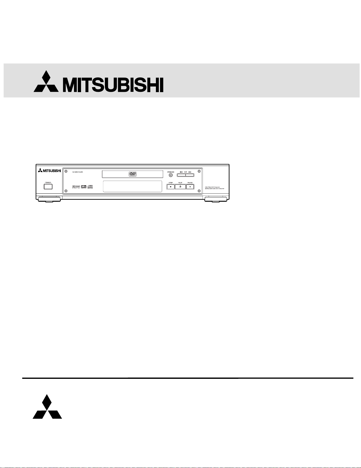
DVD PLAYER
MODEL
DD-4021
TABLE OF CONTENTS
SPECIFICATIONS .......................................................................................................................................... 1-1-1
LASER BEAM SAFETY PRECAUTIONS........................................................................................................ 1-2-1
IMPORTANT SAFETY PRECAUTIONS .......................................................................................................... 1-3-1
STANDARD NOTES FOR SERVICING .......................................................................................................... 1-4-1
CABINET DISASSEMBLY INSTRUCTIONS................................................................................................... 1-5-1
BLOCK DIAGRAMS ........................................................................................................................................ 1-6-1
SCHEMATIC DIAGRAMS / CBA’S AND TEST POINTS ................................................................................. 1-7-1
WAVEFORMS.................................................................................................................................................. 1-8-1
WIRING DIAGRAM.......................................................................................................................................... 1-9-1
SYSTEM CONTROL TIMING CHARTS ........................................................................................................ 1-10-1
IC PIN FUNCTION DESCRIPTIONS..............................................................................................................1-11-1
LEAD IDENTIFICATIONS.............................................................................................................................. 1-12-1
EXPLODED VIEWS....................................................................................................................................... 1-13-1
MECHANICAL PARTS LIST .......................................................................................................................... 1-14-1
ELECTRICAL PARTS LIST ........................................................................................................................... 1-15-1
MITSUBISHI ELECTRIC
MITSUBISHI DIGITAL ELECTRONICS AMERICA, INC.
9351 Jeronimo Road, Irvine, CA 92618-1904
Copyright © 2001 Mitsubishi Digital Electronics America, Inc.
All Rights Reserved
Page 2
HOW TO INITIALIZE THE SETUP MENU
After turning the power ON, without a disc in the tray, press the "1," "2," "3," "4," "DISPLAY" and "ENTER" buttons
on the remote control unit in this order. Then, after turning the power OFF temporarily, turn the power ON again
to intialize the Setup Menu.
HOW TO CLEAR THE PASSWORD PROTECTION
(In case the Parental Lock password is forgotten)
To release parental lock, initialize the setup menu using the procedure above.
HOW TO SET OR CLEAR THE TRAY LOCK
To set the tray lock mode to on, follow the procedures below:
1. With loading a disc, set the DVD player to the stop mode.
2. Press the "SETUP" button to display the SETUP menu.
3. Press the "TITLE" button.
4. Press the "3" button.
5. Press the "AUDIO" button.
6. Press the "0" button.
7. Press the SETUP" button. Tray Lock mode is set to ON and "Tray Lock On" is displayed on the top right of
the screen.
While the Tray Lock mode is on, the tray cannot be opened or closed. Other operations are available.
To release the Tray Lock mode, perform the above procedures again. Tray Lock mode is set to OFF and "Tray
Lock Off" is displayed on the top right of the screen.
HOW TO MANUAL EJECT
1. Remove the Top Case.
2. Insert the eject-bar (length = approximately 3 mm,
diameter = approximately 8 mm) into the manual eject
hole on the PCB Holder. Then, press it until the tray
is ejected.
3. Pull out the tray.
Tray
Top Case
PCB Holder
Manual
Eject Hole
Eject-Bar (Length = approximately 80 mm, Diameter = approximately 3 mm)
Manufatured under license from Dolby Laboratories. "Dolby" and the double-D symbol are trademarks of Dolby
Laboratories. Confidential Unpublished Works.
(©1992-1997 Dolby Laboratories, Inc. All rights reserved.)
"DTS" and "DTS Digital Out" are trademarks of Digital Theater Systems Inc.
Page 3

SPECIFICATIONS
ITEM CONDITIONS UNIT NOMINAL LIMIT
1 Video Output 75 ohm load Vpp 1.0
2 Optical Digital Out dBm -18
3 Audio(PCM)
3-1. Output Level 1kHz 0dB Vrms 2.0
3-2. S/N dB 110
3-3. Freq. Response
DVD fs=48kHz 20~22kHz dB ± 2
CD fs=44.1kHz 20~20 kHz dB ± 2
3-4. THD+N 1 kHz 0dB % 0.005
NOTES:
1. All Items are measured without pre-emphasis unless otherwise specified.
2. Power supply : AC120 V 60 Hz
3. Load imp. : 100 K ohm
4. Room ambient : +25 °C
1-1-1 E5500SP
Page 4
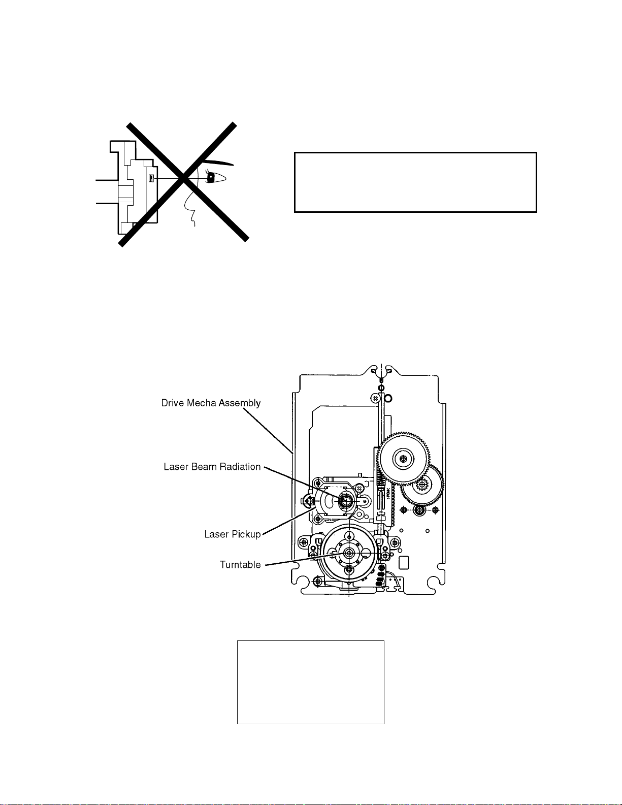
LASER BEAM SAFETY PRECAUTIONS
This DVD player uses a pickup that emits a laser beam.
Do not look directly at the laser beam coming
from the pickup or allow it to strike against
your skin.
The laser beam is emitted from the location shown in the figure. When checking the laser diode, be sure to keep your
eyes at least 30cm away from the pickup lens when the diode is turned on. Do not look directly at the laser beam.
Caution: Use of controls and adjustments, or doing procedures other than those specified herein, may result in
hazardous radiation exposure.
CAUTION
LASER RADIATION
WHEN OPEN. DO NOT
STARE INTO BEAM.
Location: Inside Top of DVD mechanism.
1-2-1 DVD_LASER
Page 5

IMPORTANT SAFETY PRECAUTIONS
Product Safety Notice
Some electrical and mechanical parts have special
safety-related characteristics which are often not evident from visual inspection, nor can the protection they
give necessarily be obtained by replacing them with
components rated for higher voltage, wattage, etc. Parts
that have special safety characteristics are identified by
a # on schematics and in parts lists. Use of a substitute replacement that does not have the same safety
characteristics as the recommended replacement part
might create shock, fire, and/or other hazards. The
Product’s Safety is under review continuously and new
instructions are issued whenever appropriate. Prior to
shipment from the factory, our products are carefully
inspected to confirm with the recognized product safety
and electrical codes of the countries in which they are
to be sold. However, in order to maintain such compliance, it is equally important to implement the following
precautions when a set is being serviced.
Precautions during Servicing
A.Parts identified by the # symbol are critical for
safety. Replace only with part number specified.
B.In addition to safety, other parts and assemblies are
specified for conformance with regulations applying
to spurious radiation. These must also be replaced
only with specified replacements.
Examples: RF converters, RF cables, noise blocking capacitors, and noise blocking filters, etc.
C.Use specified internal wiring. Note especially:
1) Wires covered with PVC tubing
2) Double insulated wires
3) High voltage leads
D.Use specified insulating materials for hazardous live
parts. Note especially:
1) Insulation tape
2) PVC tubing
3) Spacers
4) Insulators for transistors
E.When replacing AC primary side components
(transformers, power cord, etc.), wrap ends of wires
securely about the terminals before soldering.
F. Observe that the wires do not contact heat produc-
ing parts (heatsinks, oxide metal film resistors, fusible resistors, etc.).
G.Check that replaced wires do not contact sharp
edges or pointed parts.
H.When a power cord has been replaced, check that
5 - 6 kg of force in any direction will not loosen it.
I.Also check areas surrounding repaired locations.
J.Use care that foreign objects (screws, solder drop-
lets, etc.) do not remain inside the set.
K.Crimp type wire connector
The power transformer uses crimp type connectors
which connect the power cord and the primary side
of the transformer. When replacing the transformer,
follow these steps carefully and precisely to prevent
shock hazards.
Replacement procedure
1)Remove the old connector by cutting the wires at a
point close to the connector.
Important: Do not re-use a connector. (Discard it.)
2)Strip about 15 mm of the insulation from the ends of
the wires. If the wires are stranded, twist the strands
to avoid frayed conductors.
3)Align the lengths of the wires to be connected. Insert
the wires fully into the connector.
4)Use a crimping tool to crimp the metal sleeve at its
center. Be sure to crimp fully to the complete closure
of the tool.
L.When connecting or disconnecting the internal con-
nectors, first, disconnect the AC plug from the AC
outlet.
1-3-1 DVD_SFN1
Page 6
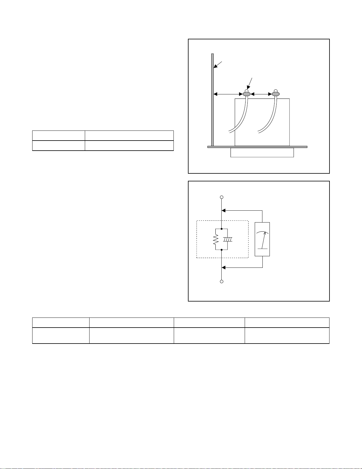
Safety Check after Servicing
Examine the area surrounding the repaired location for
damage or deterioration. Observe that screws, parts,
and wires have been returned to their original positions.
Afterwards, do the following tests and confirm the specified values to verify compliance with safety standards.
1. Clearance Distance
When replacing primary circuit components, confirm
specified clearance distance (d) and (d’) between soldered terminals, and between terminals and surrounding metallic parts. (See Fig. 1)
Table 1 : Ratings for selected area
AC Line Voltage Clearance Distance (d) (d’)
120 V ≥ 3.2 mm (0.126 inches)
Note: This table is unofficial and for reference only.
Be sure to confirm the precise values.
2. Leakage Current Test
Confirm the specified (or lower) leakage current between B (earth ground, power cord plug prongs) and
externally exposed accessible parts (RF terminals, antenna terminals, video and audio input and output terminals, microphone jacks, earphone jacks, etc.) is lower
than or equal to the specified value in the table below.
Measuring Method (Power ON) :
Insert load Z between B (earth ground, power cord plug
prongs) and exposed accessible parts. Use an AC
voltmeter to measure across the terminals of load Z.
See Fig. 2 and the following table.
Z
1.5kΩ
Chassis or Secondary Conductor
Primary Circuit Terminals
dd'
Exposed Accessible Part
AC Voltmeter
0.15µF
Earth Ground
B
Power Cord Plug Prongs
(High Impedance)
Fig. 1
Fig. 2
Table 2 : Leakage current ratings for selected areas
AC Line Voltage Load Z Leakage Current (i) Earth Ground (B) to:
120 V
Note: This table is unofficial and for reference only. Be sure to confirm the precise values.
0.15µF CAP. & 1.5kΩ RES.
Connected in parallel
i ≤ 0.5mA Peak Exposed accessible parts
1-3-2 DVD_SFN1
Page 7
STANDARD NOTES FOR SERVICING
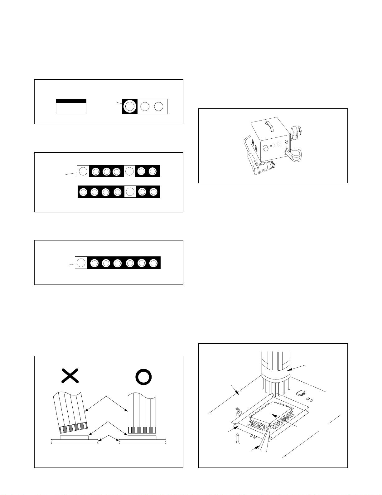
Circuit Board Indications
a.The output pin of the 3 pin Regulator ICs is indicated
as shown.
Top View
Out
b.For other ICs, pin 1 and every fifth pin are indicated
as shown.
Input
In
Pin 1
c.The 1st pin of every male connector is indicated as
shown.
Bottom View
5
10
How to Remove / Install Flat Pack-IC
1. Removal
With Hot-Air Flat Pack-IC Desoldering Machine:
(1)Prepare the hot-air flat pack-IC desoldering ma-
chine, then apply hot air to the Flat Pack-IC (about
5 to 6 seconds). (Fig. S-1-1)
Fig. S-1-1
(2)Remove the flat pack-IC with tweezers while apply-
ing the hot air.
(3)Bottom of the flat pack-IC is fixed with glue to the
CBA; when removing entire flat pack-IC, first apply
soldering iron to center of the flat pack-IC and heat
up. Then remove (glue will be melted). (Fig. S-1-6)
(4)Release the flat pack-IC from the CBA using tweez-
ers. (Fig. S-1-6)
Pin 1
Instructions for Connectors
1.When you connect or disconnect the FFC (Flexible
Foil Connector) cable, be sure to first disconnect the
AC cord.
2.FFC (Flexible Foil Connector) cable should be inserted parallel into the connector, not at an angle.
FFC Cable
Connector
CBA
Caution:
1.Do not supply hot air to the chip parts around the flat
pack-IC for over 6 seconds because damage to the
chip parts may occur. Put masking tape around the
flat pack-IC to protect other parts from damage.
(Fig. S-1-2)
2.The flat pack-IC on the CBA is affixed with glue, so
be careful not to break or damage the foil of each
pin or the solder lands under the IC when removing
it.
Hot-air
Flat Pack-IC
Desoldering
Machine
CBA
Masking
Tape
Flat Pack-IC
* Be careful to avoid a short circuit.
Tweezers
Fig. S-1-2
1-4-1 DVD_NOTE
Page 8
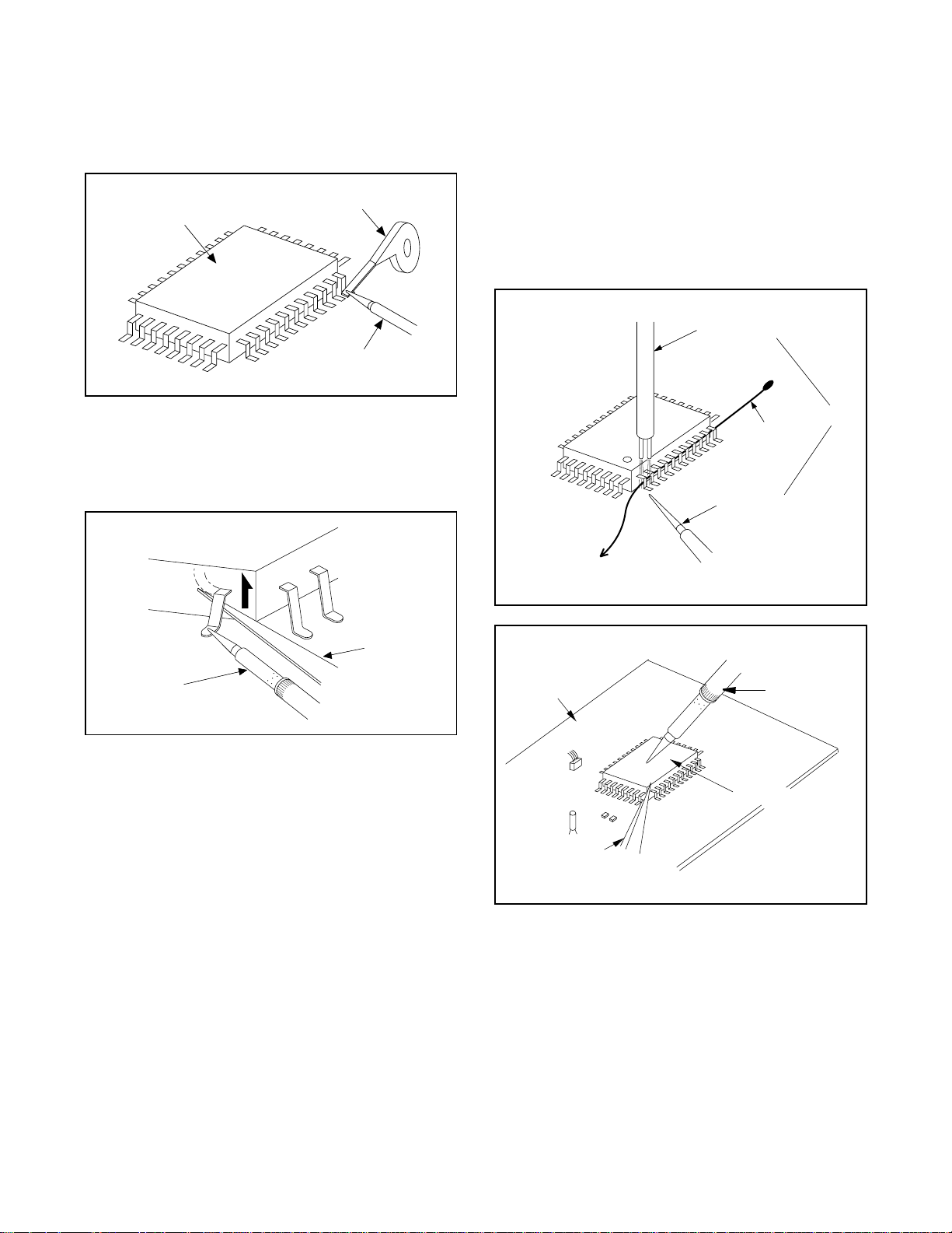
With Soldering Iron:
(1)Using desoldering braid, remove the solder from all
pins of the flat pack-IC. When you use solder flux
which is applied to all pins of the flat pack-IC, you
can remove it easily. (Fig. S-1-3)
Desoldering Braid
Flat Pack-IC
Soldering Iron
Fig. S-1-3
soldering iron to center of the flat pack-IC and heat
up. Then remove (glue will be melted). (Fig. S-1-6)
(5)Release the flat pack-IC from the CBA using tweez-
ers. (Fig. S-1-6)
Note:
When using a soldering iron, care must be taken to
ensure that the flat pack-IC is not being held by glue.
When the flat pack-IC is removed from the CBA,
handle it gently because it may be damaged if force
is applied.
Hot Air Blower
(2)Lift each lead of the flat pack-IC upward one by one,
using a sharp pin or wire to which solder will not
adhere (iron wire). When heating the pins, use a fine
tip soldering iron or a hot air desoldering machine.
(Fig. S-1-4)
Sharp
Pin
Fine Tip
Soldering Iron
Fig. S-1-4
(3)Bottom of the flat pack-IC is fixed with glue to the
CBA; when removing entire flat pack-IC, first apply
soldering iron to center of the flat pack-IC and heat
up. Then remove (glue will be melted). (Fig. S-1-6)
(4)Release the flat pack-IC from the CBA using tweez-
ers. (Fig. S-1-6)
To Solid Mounting Point
CBA
Tweezers
Iron Wire
or
Soldering Iron
Fig. S-1-5
Fine Tip
Soldering Iron
Flat Pack-IC
With Iron Wire:
(1)Using desoldering braid, remove the solder from all
pins of the flat pack-IC. When you use solder flux
which is applied to all pins of the flat pack-IC, you
can remove it easily. (Fig. S-1-3)
(2) Affix the wire to a workbench or solid mounting point,
as shown in Fig. S-1-5.
(3)While heating the pins using a fine tip soldering iron
or hot air blower, pull up the wire as the solder melts
so as to lift the IC leads from the CBA contact pads
as shown in Fig. S-1-5.
(4)Bottom of the flat pack-IC is fixed with glue to the
CBA; when removing entire flat pack-IC, first apply
Fig. S-1-6
1-4-2 DVD_NOTE
Page 9
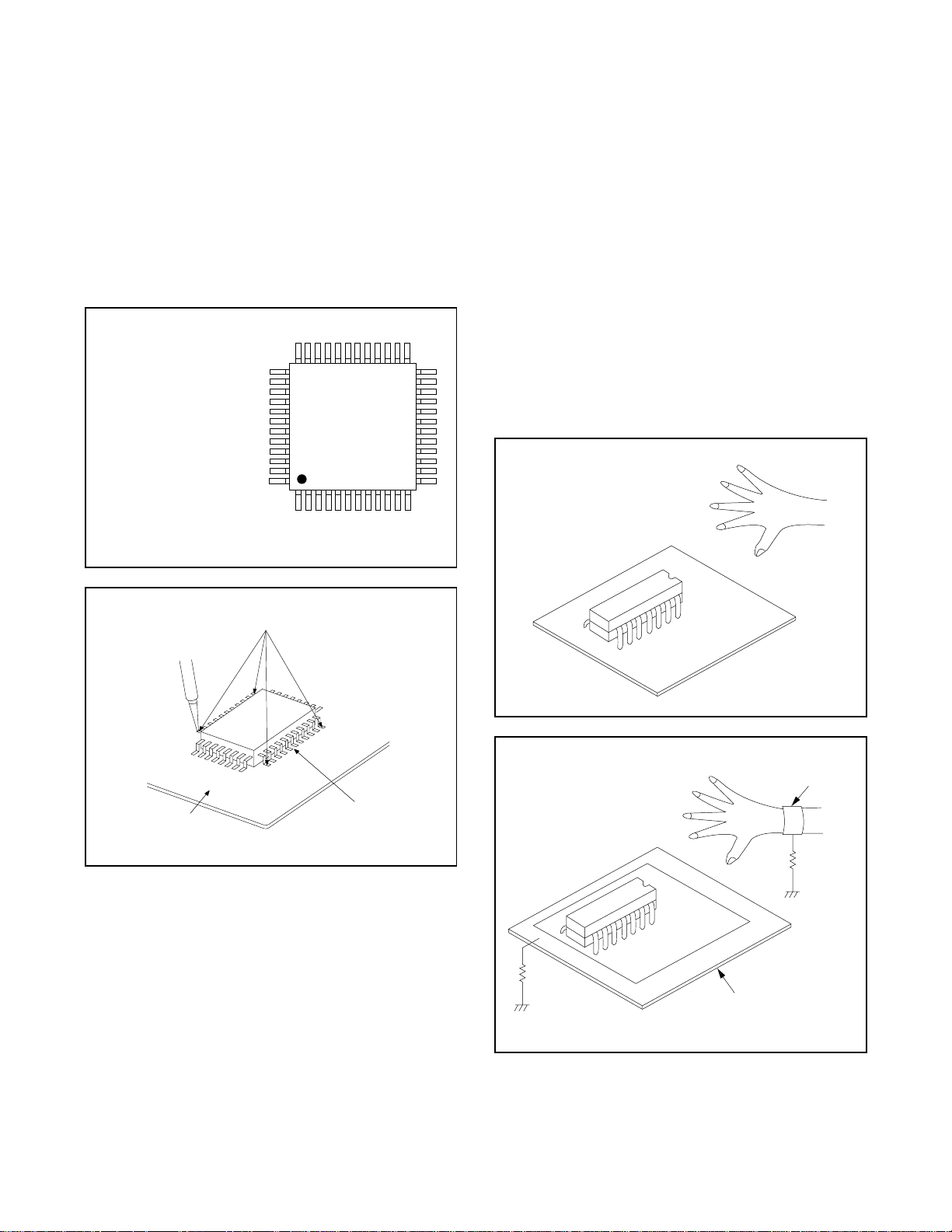
2. Installation
(1)Using desoldering braid, remove the solder from the
foil of each pin of the flat pack-IC on the CBA so you
can install a replacement flat pack-IC more easily.
(2)The " ● " mark on the flat pack-IC indicates pin 1.
(See Fig. S-1-7.) Be sure this mark matches the 1
on the PCB when positioning for installation. Then
pre- solder the four corners of the flat pack-IC. (See
Fig. S-1-8.)
(3)Solder all pins of the flat pack-IC. Be sure that none
of the pins have solder bridges.
Example :
Pin 1 of the Flat Pack-IC
is indicated by a " ● " mark.
Fig. S-1-7
Instructions for Handling
Semiconductors
Electrostatic breakdown of the semiconductors may
occur due to a potential difference caused by electrostatic charge during unpacking or repair work.
1. Ground for Human Body
Be sure to wear a grounding band (1MΩ) that is properly
grounded to remove any static electricity that may be
charged on the body.
2. Ground for Workbench
Be sure to place a conductive sheet or copper plate with
proper grounding (1MΩ) on the workbench or other
surface, where the semiconductors are to be placed.
Because the static electricity charge on clothing will not
escape through the body grounding band, be careful to
avoid contacting semiconductors with your clothing.
< Incorrect >
Soldering Iron
CBA
Presolder
CBA
< Correct >
Grounding Band
Flat Pack-IC
Fig. S-1-8
1MΩ
CBA
1MΩ
Conductive Sheet or
Copper Plate
1-4-3 DVD_NOTE
Page 10
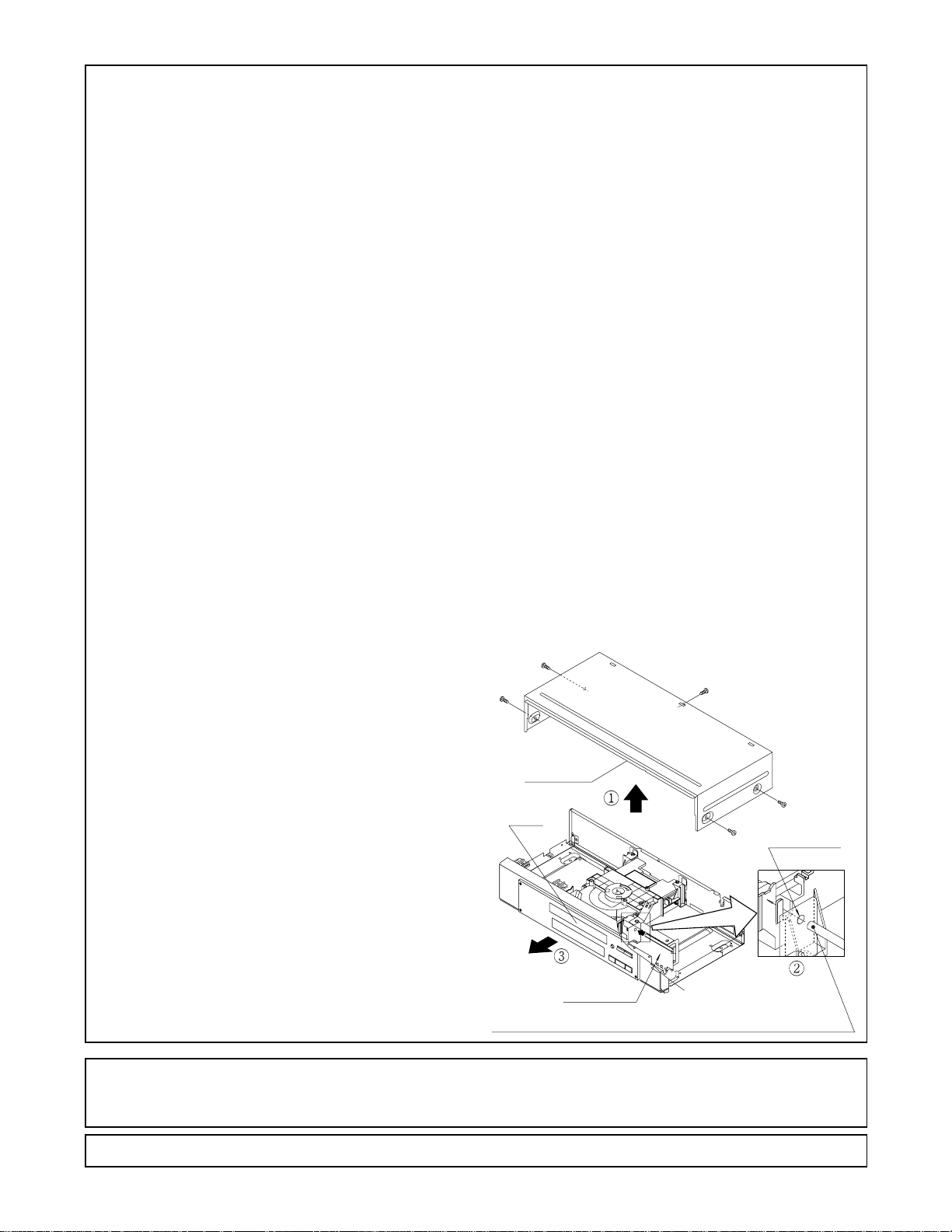
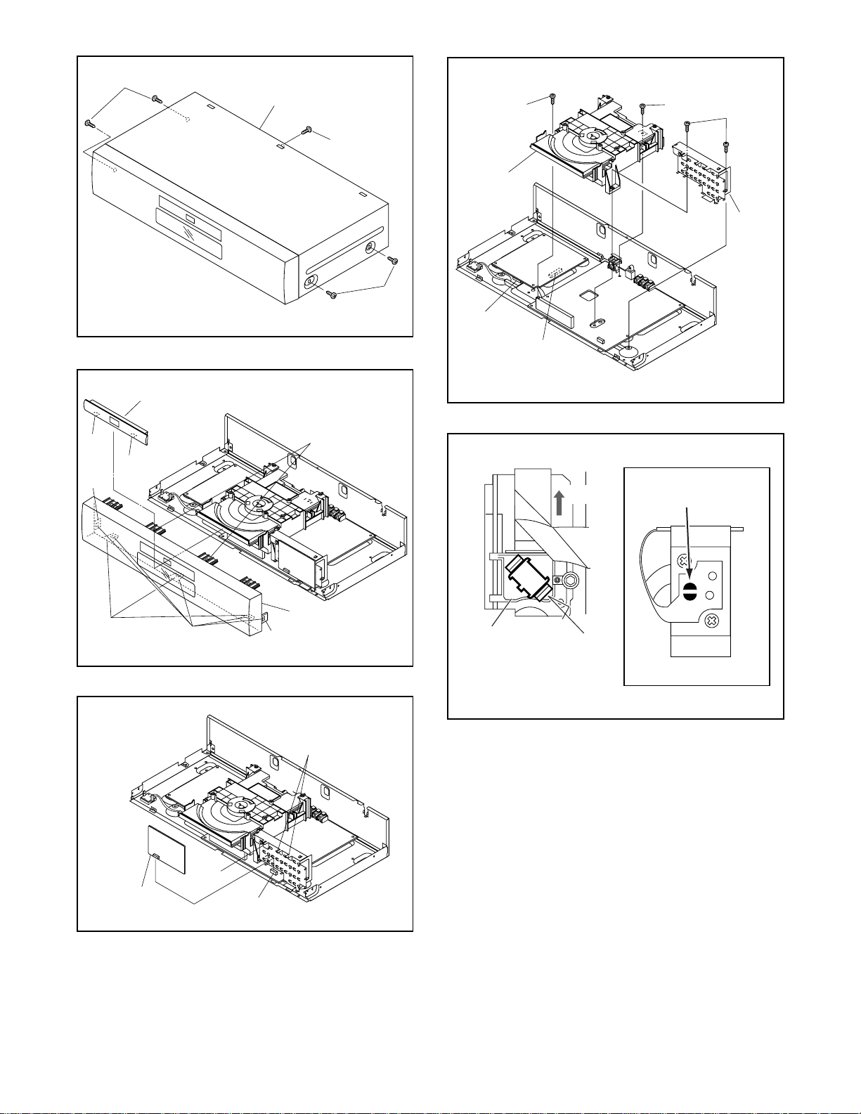
CABINET DISASSEMBLY INSTRUCTIONS
1. Disassembly Flowchart
This flowchart indicates the disassembly steps to gain
access to item(s) to be serviced. When reassembling,
follow the steps in reverse order. Bend, route, and dress
the cables as they were originally.
2. Disassembly Method
[1] Top Case
[2] Front Assembly
[3] Function CBA
[4] PCB Holder
[5] DVD Mecha
[7] DVD Main CBA Unit[6] AV CBA
[8] Rear Panel
REMOVAL
ID/
LOC.
No.
[1] Top Case 1 5(S-1) -
[2]
[3]
[4]
[5]
[6] AV CBA 6
[7]
[8]
↓
➀
PART
Front
Assembly
Function
CBA
PCB
Holder
DVD
Mecha
DVD
Mecha
CBA Unit
Rear
Panel
↓
➁
REMOVE/
Fig.
*UNHOOK/UNLOCK/
No.
RELEASE/UNPLUG/
DESOLDER
*2(L-1), Tray Panel,
2
*2(L-2), *5(L-3)
3 *3(L-4), *(CN2001) -
42(S-2) -
*(CN001, CN201),
4,5
2(S-3)
4(S-4), 4(S-5),
*2(L-5), *(CN701,
CN501)
64(S-6) -
73(S-7) -
↓
➂
↓
➃
Note
1-1
1-2
2-1
2-2
2-3
3
-
↓
➄
1 : Identification (location) No. of parts in the figures
2 : Name of the part
3 : Figure Number for reference
4 : Identification of parts to be removed, unhooked, un-
locked, released, unplugged, unclamped, or
desoldered.
P=Spring, L=Locking Tab, S=Screw,
CN=Connector
*=Unhook, Unlock, Release, Unplug, or Desolder
e.g. 2(S-2) = two Screws (S-2),
2(L-2) = two Locking Tabs (L-2)
5 :Refer to "Reference Notes."
Reference Notes
CAUTION 1: Locking Tabs (L-1) are fragile. Be careful
not to break them.
1-1.Connect the wall plug to an AC outlet and press the
OPEN/CLOSE button to open the Tray.
1-2.First, remove the Tray Panel by releasing two Lock-
ing Tabs (L-1). Second, release two Locking Tabs
(L-2). Then, release five Locking Tabs (L-3) (to do
this, first release three Locking Tabs (A) at the
bottom, and then two Locking Tabs (B) at the side.)
(Fig. 2)
CAUTION 2: Electrostatic breakdown of the laser diode
in the optical system block may occur as a potential
difference caused by electrostatic charge accumulated
on cloth, human body etc, during unpacking or repair
work.
To avoid damage of pickup follow next procedures.
2-1.Slide out the pickup unit as shown in Fig. 5.
2-2.Short the copper pattern (half-moon shape) of FPC
cable with solder before removing the FFC cable
(CN001) from it. If you disconnect the FFC cable
(CN001), the laser diode of pickup will be destroyed.
(Fig. 5)
2-3.Disconnect Connector (CN201). Remove two
Screws (S-3) and lift the DVD Mecha. (Fig. 4)
CAUTION 3: When reassembling, confirm the FFC
cable (CN001) is connected completely. Then remove
the solder from copper pattern (half-moon shape) of
FPC cable. (Fig. 5)
1-5-1 E5540DC
Page 11
(S-1)
[1] Top Cover
(S-1)
(S-1)
(S-3)
[5] DVD
Mecha
(S-3)
(S-2)
[4] PCB
Holder
(L-1)
(B)
(A)
(L-1)
Tray Panel
(L-3)
(L-2)
[2] Front Assembly
(B)
Fig. 1
Fig. 2
CN201
CN001
Pickup Unit
DVD Mecha
Bottom View
Slide
A
Fig. 4
Short the copper pattern
by soldering
View for A
Fig. 5
[3] Function
CBA
(L-4)
CN2001
(L-4)
Fig. 3
1-5-2 E5540DC
Page 12
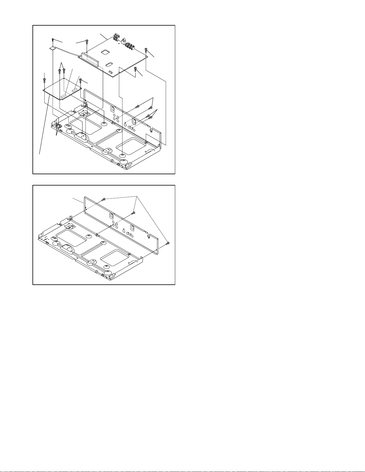
[6] AV CBA
(S-5)
(S-6)
(S-6)
(L-5)
[7] DVD Main CBA Unit
[8] Rear Panel
CN501
CN701
(S-6)
(S-5)
(S-5)
(S-4)
(S-4)
Fig. 6
(S-7)
Fig. 7
1-5-3 E5540DC
Page 13
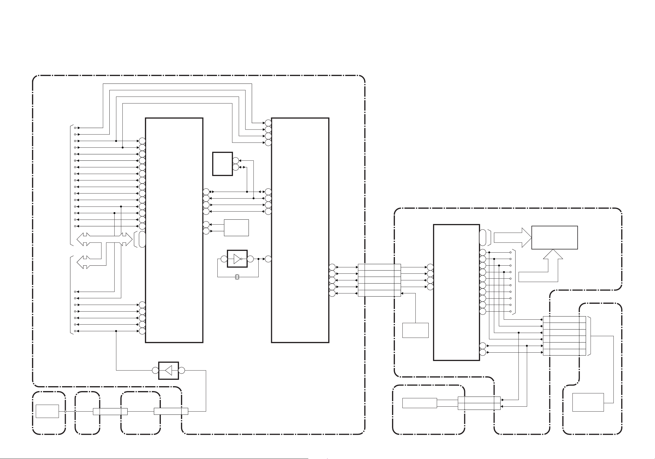
System Control Block Diagram
BLOCK DIAGRAMS
FROM/TO
RF SIGNAL
PROCESS
/SERVO
BLOCK
DIAGRAM
FROM/TO
DVD SIGNAL
PROCESS
BLOCK
DIAGRAM
TFW
TREV
TIN
TOUT
SCLKH
SDATA
CSL
MUTE
PS
RS
HINT
HCS
HWR
HRD
HA0
HA1
HRD
HWR
JITTER
MRDY
MCS
MALE
FG
HD0-HD7
IC400
(FRONT END PROCESSOR)
TIN
60
61
TOUT
3 SCLKH
4 SDATA
5 CSL
99 MUTE
100
PS
1 RS
51 HINT
95 HCS
HWR
10
HRD
8
HA0
92
HA1
93
HD0
83
~
~
HD7
90
37 JITTER
14 MRDY
94 MCS
7 MALE
52 FG
IC002
(OP AMP)
RDY-HIF
/FERS
XOUT8180
SDA
SCL
XIN
IC603
(MEMORY)
25
26
30
50
SCL
6
5
SDA
X401
16MHz
IC608
(INVERTER)
2 4
X601
27MHz
IC601
(DVD HOST PROCESSOR)
TFW
200
TREV
201
187
TIN
TOUT
188
SDA
196
SCL
195
RDY-HIF
208
186
/FERS
CLOCK
120
VFD-DOUT
VFD-CLK
REMOTE
3VFD-STB
1VFD-DIN
2
204
125
CN501 CN1001
FP-STB 19
19
FP-DIN 20
20
FP-DOUT 21
21
FP-CLK 22
22
REMOTE 24
24
RM2001
REMOTE
SENSOR
IC2003
(FRONT PANEL CONTROL)
1G
~
11G
a/KEY-1
b/KEY-2
9
FP-STB
7
FP-DIN
6
FP-DOUT
FP-CLK
8
c/KEY-3
d/KEY-4
e
f
g
h
i
j
K2
K1
42
32
14
15
16
17
18
19
20
21
22
23
11
10
FL2002
~
GRID FIP
SEGMENT
CN2001
KEY-4 1
1
KEY-3 2
2
KEY-2 3
3
KEY-1 4
4
K2 5
5
K1 6
6
CN2003
FG
SENSOR
CN3004 CN3003
FG-IN 6
6
INNER
CBA
1 3
FG-IN 10
1-6-1
CN201
MAIN CBA UNIT
POWER SW
SWITCH CBAFG CBA MECHA CBA
AV CBA
KEY-2 1
1
K2 2
2
JP1003JP1004
1-6-2
KEY MATRIX
FUNCTION CBA
E5542BLS
Page 14
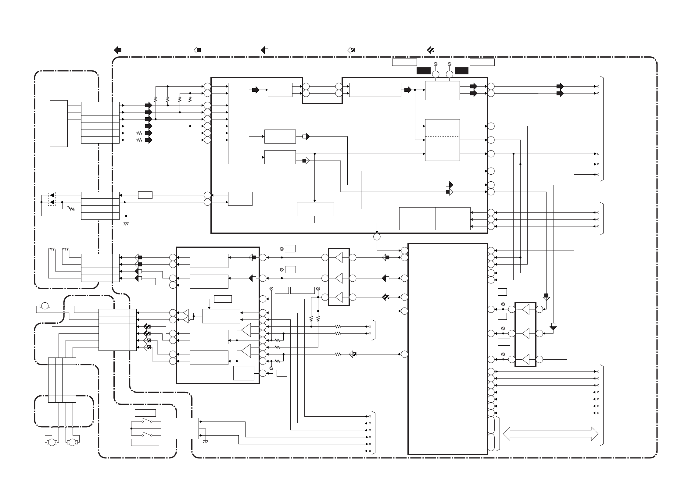
RF Signal Process/Servo Block Diagram
PICK-UP UNIT
DETECTOR
A 3
D 4
C 1
B 2
F 7
E 8
LD 11
MON 12
GND 9
GND 10
RF(VIDEO/AUDIO) SIGNAL FOCUS SERVO SIGNAL TRACKING SERVO SIGNAL
IC001
(RF SIGNAL PROCESS)
17
18
FOCUS ON
GATE SIGNAL
CN001
CN001
Q001
AMP
29
30
28
25
26
27
40
39
60
58
RF
AMP
INPUT
MATRIX
TRACKING
ERROR DET
FOCUS
ERROR DET
PB-ALPC
SLIDE SERVO SIGNAL DISK SERVO SIGNAL
16
15
AGC AMP
PROGRAMMABLE EQ
MONREF MONREP
TP001 TP002
WF1 WF2
DATA SLICER
ASYMMETRY
CONTROL
MIRROR DET
DEFECT DET
CONTROL
REGISTERS
5 6
MCU
I/F
76
77
69
74
73
51
52
53
66
67
68
MAIN CBA UNIT
NRZN
NRZP
DEFECT
TC
SRV33M
SCLKH
SDATA
CSL
TO DVD SIGNAL
PROCESS
BLOCK DIAGRAM
FROM
SYSTEM CONTROL
BLOCK DIAGRAM
LOADING
MOTOR
M
CN3004 CN3003
M M
SPINDLE
MOTOR
SPL(-) 11
FSTS
SL(-) 33
SPL(+) 22
SLIDE
MOTOR
SL(+) 44
INNER
FS(+) 17
FS(-) 16
TS(+) 15
TS(-) 18
SPL(-) 6
SPL(+) 7
CBA
MECHA CBA
CN001
LD(+) 1
LD(-) 2
SL(+) 9
SL(-) 8
CN201
TRAY-IN
TRAY-OUT
IC200 (SERVO DRIVE)
12 6
11
14
13
10
9
18
17
16
15
TRAY-IN 3
GND 5
TRAY-OUT 4
FOCUS
DRIVE
TRACKING
DRIVE
MUTE
LOADING
MOTOR DRIVE
SPINDLE
MOTOR DRIVE
SLIDE
MOTOR DRIVE
POWER
SAVE
CN201
TP202
FS
TP201
TS
5
TP203
PWM
21
1
2
24
+
-
23
22
27
+
-
26
25
TP205
4
SL
TP104
VREF165
IC002
(OP AMP)
14 12
8 10
7 5
PWM1
PWM2
MUTE
TREV
TRAY-IN
TRAY-OUT
70
FROM
DVD SIGNAL
PROCESS
BLOCK
TFW
FROM/TO
SYSTEM
CONTROL
BLOCK
PS
IC100 (SERVO DSP)
41
PDM2
3 52
PDM0
7
1
PDM3
19
ADC4
PDM1
5
CLKINFSGATE
TC
MIRROR
TZC
DEFECT
ADC1
ADC0
ADC2
RS
HINT
HCS
HWR
HRD
HA0
HA1
HD0
~
HA7
95
27
26
34
FE
IC102
(OP AMP)
TP103
22 10
23
21 14 12
68
76
77
78
79
81
80
90
86
84
82
8
TE
TP102
1 3
ASO
TP101
~
~
HD0-HD7
RS
HINT
HCS
HWR
HRD
HAO
HA1
FROM/TO
SYSTEM CONTROL
BLOCK DIAGRAM
1-6-4
E5542BLRF1-6-3
Page 15

DVD Signal Process Block Diagram
IC300 (DVD SIGNAL PROCESS)
WF4
WF5
FROM RF SIGNAL
PROCESS/SERVO
BLOCK DIAGRAM
NRZN
NRZP
TC
DEFECT
118
117
94
95
DATA(VIDEO/AUDIO) SIGNAL DATA(VIDEO) SIGNAL DATA(AUDIO) SIGNALRF(VIDEO/AUDIO) SIGNAL
MAIN CBA UNIT
PLL
VCO
HD0
24
27
HD1
HD2
DATA
SLICER
BCA
DVD
DEMODULATOR
VIDEO/AUDIO
INTERFACE
HD3
HD4
HD5
HD6
HD7
30
34
37
40
43
46
HD0-HD7
TO VIDEO BLOCK
FROM/TO
SYSTEM CONTROL
BLOCK DIAGRAM
TO RF SIGNAL
PROCESS/SERVO
BLOCK DIAGRAM
HD0-HD8
MCS
JITTER
MRDY
HRD
HWR
MALE
FG
X301 (33MHz)
SRV33M
PWM1
PWM2
HD0
69
~
~
HD7
77
86
MCS
124
JITTER
83 MRDY
81 HRD
79 HWR
80 MALE
155
156
57
99
100
101
MASTER
CLOCK
CLV/CAV
CPU
INTERFACE
MEMORY
MANAGER
IC301 (4M D-RAM)
RAS
189
174
UCAS
173
LCAS
190
WE
175
OE
RA0 RA0
187
~
RD0
~
RD15 2
~
177
207
~
191
1
RA0-RA8
RD0-RD15
14
28
29
13
27
16
~
26
2
~
10
31
~
39
RAS
UCAS
LCAS
WE
OE
~
RA8RA8
RD0
~
RD15
1-6-6
E5542BLD1-6-5
Page 16

Video Block Diagram
DATA(VIDEO) SIGNAL VIDEO SIGNAL AUDIO SIGNALDATA(AUDIO) SIGNAL
IC601 (DVD HOST PROCESSOR)
FROM
DVD SIGNAL
PROCESS
BLOCK
PARA0-PARA7
6
13
PARA0
~
PARA7
~
INTERNAL
PERIPHERALS
PORTS
CPU
CENTRAL
COMMAND
PORT
ST20 ARBITER &
MEMORY CONTROLLER
MPEG2 PER
PARSER & MPEG1
SYSTEM PARSER
VIDEO
CD FIFO
AUDIO
CD FIFO
DATA(VIDEO/AUDIO) SIGNAL DATA(VIDEO) SIGNAL
CACHE
SUBSYSTEM
FRONT-END
& LINK
INTERFACE
AUDIO
DECODER
SUB
PICTURE
CD FIFO
51
52
53
54
55
56
57
PCM-SCLK
PCM-DATA0
PCM-DATA1
PCM-DATA2
PCM-MCLK
PCM-LRCLK
SPDIF
TO AUDIO
BLOCK
Q1481, Q1482
6dB AMP
Q1461, Q1462
6dB AMP
Q1483
75Ω
BUFFER
Q1463
75Ω
BUFFER
Q1443
75Ω
BUFFER
JK1202
VIDEO-V
OUT
VIDEO-U
OUT
VIDEO-Y
OUT
IC602
(16M SD-RAM)
A0
~
A18
DQ0
~
DQ15
WE
CE
OE
25
16
29
45
11
26
28
8
1
~
~
~
A0-A18
DQ0-DQ15
161
170
173
181
141
158
128
132
117
~
A0
A18
~
DQ0
~
DQ15
DQM(0)
CS3
OE
~
PROGRAMMABLE
CPU INTERFACE
~
SHARED SDRAM INTERFACE
~
AD0
AD13
58 63~69 66~ 84
20 26~ 2 13~29 35~ 42 53~
~
AD0
AD13
VIDEO
DECODER
~
DQ0
DQ15
102
~70 73~
~
DQ0
DQ15
SDRAM ARBITER
VIDEO
FILTERING
DQML
DQMU
LDQM
UDQM
WE
WE
RAS
CAS
79 80 78
7677
17 18 39 16
15
RAS
CAS
OSD, SP
DECODER
& MIXING
DENC &
DAC
27
25
34
33
32
WF5
CN701
1 1VIDEO-V
3 3VIDEO-U
5 5VIDEO-Y
7 7
VIDEO-CVBS
9 9VIDEO-C
WF7WF6
CN1601
Q1441, Q1442
6dB AMP
Q1401, Q1402
6dB AMP
Q1421, Q1422
6dB AMP
Q1445
75Ω
AMP
BUFFER
Q1423
75Ω
BUFFER
Q1403
75Ω
BUFFER
3 4
3 4
21
21
JK1401
S-VIDEO
OUT
JK1201
COMPOSITE
VIDEO OUT
AV CBA
IC606
(64Mbit SDRAM)
MAIN CBA UNIT
1-6-8
E5542BLV1-6-7
Page 17

Audio Block Diagram
VIDEO SIGNAL AUDIO SIGNALDATA(AUDIO) SIGNAL
FROM
VIDEO
BLOCK
FROM
SYSTEM
CONTROL
BLOCK
SPDIF
PCM-SCLK
PCM-DATA0
PCM-LRCK
ADAC-MD
ADAC-MC
ADAC-ML
WF11WF10
WF9
IC801 (AUDIO DAC)
1
2
3
13
14
15
SERIAL
PORT
SERIAL
CONTROL
4X/8X
OVERSAMPLING
DIGITAL FILTER
/FUNCTION
CONTROLLER
ENPHANCED
MULTI-LEVEL
DELTA-SIGMA
MODULATOR
ZERP DETECT
SYSTEM CLOCK
16
DAC LPF+AMP
DAC
LPF+AMP
L-CH
R-CH
7
8
12
11
WF12
CN701
1212SPDIF
CN701 CN1601
15 15AUDIO-L
1717AUDIO-R
14 14A-L MUTE
16 16A-R MUTE
18 18A-MUTE
CN1601
REF
Q1204
3
2
6
5
+3.3V
Q1203
IC1201
Q1351
AMP
(AMP)
1
7
Q1202
JK1202
DIGITAL
AUDIO OUT
JK1201
AUDIO-L
OUT
AUDIO-R
OUT
Q1201
TO
VIDEO
BLOCK
PCM-MCLK
A-MUTE
+3.3V
MAIN CBA UNIT
1-6-9 1-6-10
AV CBA
E5542BLA
Page 18

Power Supply Block Diagram
CAUTION !
Fixed voltage power supply circuit is used in this unit.
If Main Fuse (F1001) is blown, check to see that all components in the
power supply circuit are not defective before you connect the AC plug to
the AC power supply. Otherwise it may cause some components in the
power supply circuit to fail.
AC1001
AC CORD
F1001
1A 250V
F
A V
L1001
CHOKE
COIL
D1001, D1002
D1004, D1005
BRIDGE
RECTIFIER
Q1003
SWITCHING
CONTROL
A V
Q1001
SWITCHING
CAUTION
FOR CONTINUED PROTECTION AGAINST FIRE HAZARD,
F
REPLACE ONLY WITH THE SAME TYPE FUSE.
ATTENTION : POUR UNE PROTECTION CONTINUE LES RISQES
D'INCELE N'UTILISER QUE DES FUSIBLE DE MEMO TYPE.
RISK OF FIRE
"This symbol means fast operating fuse."
"Ce symbole reprèsente un fusible à fusion rapide."
-REPLACE FUSE AS MARKED.
T1001
2
4
7
11
12
13
14
15
16
17
D1003
RECTIFIER
D1030
RECTIFIER
D1008
RECTIFIER
D1009
RECTIFIER
D1013
RECTIFIER
D1016
RECTIFIER
Q1010
Q1002
Q1006
IC1004
+3.3V
REG.
+12V
REG.
Q1007
REG
Q1004
IC1003
Q1005
NOTE :
The voltage for parts in hot circuit is measured using
hot GND as a common terminal.
IC302
CN1001
1
EV+2.5V
2
EV+2.5V
3
P-ON+5V
4
P-ON+5V
12
EV+9V
13
EV+9V
14
EV+3.3V
15
EV+3.3V
16
P-ON+3.3V
17
P-ON+3.3V
18
PWRCON
CN501
1
2
3
4
12
13
14
15
16
17
18
+3.3V
5 4
REG.
P-ON+3.3V(A)
EV+2.5V
P-ON+5V(D)
P-ON+5V(A)
EV+9V
EV+3.3V
P-ON+3.3V(D)
PWRCON
MAIN CBA UNIT
FROM
SYSTEM
CONTROL
BLOCK
DIAGRAM
Q1008
LATCH
HOT
AV CBA
6
IC1001
ERROR
VOLTAGE DET
4
3
18
1
2
Q1009
(SHUNT REGULATOR)
REG
COLD
1-6-12
P-ON+12V
F2
F1
-FL
P-ON+5V
P-ON+3.3V
EV+5V
E5542BLP1-6-11
Page 19

SCHEMATIC DIAGRAMS / CBA’S AND TEST POINTS
Standard Notes
Warning
Many electrical and mechanical parts in this chassis
have special characteristics. These characteristics
often pass unnoticed and the protection afforded by
them cannot necessarily be obtained by using replacement components rated for higher voltage, wattage, etc.
Replacement parts that have these special safety characteristics are identified in this manual and its supplements; electrical components having such features are
identified by the mark " #" in the schematic diagram
and the parts list. Before replacing any of these components, read the parts list in this manual carefully. The
use of substitute replacement parts that do not have the
same safety characteristics as specified in the parts list
may create shock, fire, or other hazards.
Capacitor Temperature Markings
Mark
(B) ±10% 20°C -25~+85°C
(F) +30 -80% 20°C -25~+85°C
(SR) ±15% 20°C -25~+85°C
(Z) +30 -80% 20°C -10~+70°C
Capacity
change rate
Standard
temperature
Temperature
range
Note:
1.Do not use the part number shown on these drawings for ordering. The correct part number is shown
in the parts list, and may be slightly different or
amended since these drawings were prepared.
2.
All resistance values are indicated in ohms (K=10
6
M=10
).
3.Resistor wattages are 1/4W or 1/6W unless otherwise specified.
4.All capacitance values are indicated in µF
−6
(P=10
5.All voltages are DC voltages unless otherwise specified.
µF).
3
,
Capacitors and transistors are represented by the following symbols.
CBA Symbols
(Top View) (Bottom View)
+
Electrolytic Capacitor
(Bottom View)
Transistor or Digital Transistor
E C B
(Top View)
NPN Transistor
E C B
(Top View)
NPN Digital Transistor
E C B
(Top View)
E C B
(Top View)
E C B
Schematic Diagram Symbols
Digital Transistor
PNP Transistor
PNP Digital Transistor
1-7-1 DVD_SC01
Page 20

LIST OF CAUTION, NOTES, AND SYMBOLS USED IN THE SCHEMATIC DIAGRAMS ON THE FOLLOWING
PAGES:
1. CAUTION:
FOR CONTINUED PROTECTION AGAINST FIRE HAZARD, REPLACE ONLY WITH THE SAME
F
A V
TYPE FUSE.
ATTENTION: POUR UNE PROTECTION CONTINUE LES RISQES D’INCELE N’UTILISER QUE
DES FUSIBLE DE MEMO TYPE.
RISK OF FIRE-REPLACE FUSE AS MARKED.
This symbol means fast operating fuse.
2. CAUTION:
Ce symbole represente un fusible a fusion rapide.
Fixed Voltage (or Auto voltage selectable) power supply circuit is used in this unit.
If Main Fuse (F001) is blown, first check to see that all components in the power supply circuit are not defective
before you connect the AC plug to the AC power supply. Otherwise it may cause some components in the power
supply circuit to fail.
3. Note:
(1)Do not use the part number shown on the drawings for ordering. The correct part number is shown in the parts
list, and may be slightly different or amended since the drawings were prepared.
(2)To maintain original function and reliability of repaired units, use only original replacement parts which are listed
with their part numbers in the parts list section of the service manual.
4. Wire Connectors
(1)Prefix symbol "CN" means "connector" (can disconnect and reconnect).
(2)Prefix symbol "CL" means "wire-solder holes of the PCB" (wire is soldered directly).
5. Note: Mark "•" is a leadless (chip) component.
6. Mode: SP
7. Voltage indications for PLAY mode on the schematics are as shown below:
PLAY mode
5.0
231
5.0
Indicates that the voltage
is not consistent here.
8. How to read converged lines
1-D3
Distinction Area
Line Number
(1 to 3 digits)
Examples:
1. "1-D3" means that line number "1" goes to area "D3".
2. "1-B1" means that line number "1" goes to area "B1".
3
AREA D3
2
1
1-D3
ABCD
Unit: Volts
1-B1
AREA B1
9. Test Point Information
: Indicates a test point with a jumper wire across a hole in the PCB.
: Used to indicate a test point with a component lead on foil side.
: Used to indicate a test point with no test pin.
: Used to indicate a test point with a test pin.
1-7-2 DVD_SC02
Page 21

Main 1/5 Schematic Diagram
1-7-3
1-7-4
1-7-5
E5542SCM1
Page 22

Main 2/5 Schematic Diagram
1-7-6 1-7-7
1-7-8
E5542SCM2
Page 23

Main 3/5 Schematic Diagram
1-7-9
1-7-10
1-7-11
E5542SCM3
Page 24

Main 4/5 Schematic Diagram
1-7-12
1-7-13
1-7-14
E5542SCM4
Page 25

Main 5/5 Schematic Diagram
1-7-15 1-7-16
E5542SCM5
Page 26

AV 1/3 Schematic Diagram
CAUTION !
Fixed voltage power supply circuit is used in this unit.
If Main Fuse (F1001) is blown, check to see that all components in the power supply circuit
are not defective before you connect the AC plug to the AC power supply. Otherwise it may
cause some components in the power supply circuit to fail.
NOTE :
The voltage for parts in hot circuit is measured
using hot GND as a common terminal.
F
A V
CAUTION
FOR CONTINUED PROTECTION AGAINST FIRE HAZARD,
REPLACE ONLY WITH THE SAME TYPE FUSE.
ATTENTION : POUR UNE PROTECTION CONTINUE LES RISQES
D'INCELE N'UTILISER QUE DES FUSIBLE DE MEMO TYPE.
RISK OF FIRE-REPLACE FUSE AS MARKED.
"This symbol means fast operating fuse."
"Ce symbole reprèsente un fusible à fusion rapide."
1-7-17 1-7-18 E5542SCAV1
Page 27

AV 2/3 Schematic Diagram
1-7-19
1-7-20
E5542SCAV2
Page 28

AV 3/3 & Function Schematic Diagram
PBCCDVIDEODVDB
CHP
TTL TRK
A
11G 9G10G 8G 7G 6G 5G 4G 3G 2G 1G
a
b
c
d
e
f
g
c
d
e
f
g
h
i
j
c
d
e
f
g
c
d
e
f
g
c
d
e
f
g
h
i
c
d
e
f
g
c
d
e
f
g
c
d
e
f
g
c
d
e
f
g
c
d
e
f
g
c
d
e
f
g
h
i
j
a
b
a
b
c
d
e
f
g
a
b
a
b
a
b
a
b
a
b
a
b
a
b
a
b
a
b
FL2001 MATRIX CHART
TRK
DVD CD PBC
CHP
AB
10G11G
a
j
b
i
h
c
d
g
e
f
9G
7G8G
a
cb
d
e
f
gh
i
6G
5G
jj
4G
i
i
3G
2G
i
i
1G
a
cb
d
ef
g
1-7-21 1-7-22 E5542SCAV3
Page 29

AV CBA Top View
CAUTION !
Fixed voltage power supply circuit is used in this unit.
If Main Fuse (F1001) is blown, check to see that all components in the power
supply circuit are not defective before you connect the AC plug to the AC
power supply.
Otherwise it may cause some components in the power supply circuit to fail.
CAUTION
FOR CONTINUED PROTECTION AGAINST FIRE HAZARD,
F
A/ V
REPLACE ONLY WITH THE SAME TYPE FUSE.
ATTENTION : POUR UNE PROTECTION CONTINUE LES RISQES
D'INCELE N'UTILISER QUE DES FUSIBLE DE MEMO TYPE.
RISK OF FIRE-REPLACE FUSE AS MARKED.
"This symbol means fast operating fuse."
"Ce symbole reprèsente un fusible à fusion rapide."
BECAUSE A HOT CHASSIS GROUND IS PRESENT IN THE POWER
SUPPLY CIRCUIT, AN ISOLATION TRANSFORMER MUST BE USED.
ALSO, IN ORDER TO HAVE THE ABILITY TO INCREASE THE INPUT
SLOWLY, WHEN TROUBLESHOOTING THIS TYPE POWER SUPPLY
CIRCUIT, A VARIABLE ISOLATION TRANSFORMER IS REQUIRED.
1-7-23
1-7-24
BE5500F01016-A
Page 30

AV CBA Bottom View
Switch CBA
Top View
Switch CBA
Bottom View
BE5500F01016-B
CAUTION !
Fixed voltage power supply circuit is used in this unit.
If Main Fuse (F1001) is blown, check to see that all components in the power
supply circuit are not defective before you connect the AC plug to the AC
power supply.
Otherwise it may cause some components in the power supply circuit to fail.
CAUTION
FOR CONTINUED PROTECTION AGAINST FIRE HAZARD,
F
A/ V
BECAUSE A HOT CHASSIS GROUND IS PRESENT IN THE POWER
SUPPLY CIRCUIT, AN ISOLATION TRANSFORMER MUST BE USED.
ALSO, IN ORDER TO HAVE THE ABILITY TO INCREASE THE INPUT
SLOWLY, WHEN TROUBLESHOOTING THIS TYPE POWER SUPPLY
CIRCUIT, A VARIABLE ISOLATION TRANSFORMER IS REQUIRED.
REPLACE ONLY WITH THE SAME TYPE FUSE.
ATTENTION : POUR UNE PROTECTION CONTINUE LES RISQES
D'INCELE N'UTILISER QUE DES FUSIBLE DE MEMO TYPE.
RISK OF FIRE-REPLACE FUSE AS MARKED.
"This symbol means fast operating fuse."
"Ce symbole reprèsente un fusible à fusion rapide."
1-7-25
1-7-26
BE5500F01016-A
Page 31

Function CBA Top View
Function CBA Bottom View
1-7-27
1-7-28
BE5560F01013
Page 32

WAVEFORMS
WF1
MONREF
WF2
Pin 5 of IC001
0.2V 0.2usec
Pin 6 of IC001
WF5
WF6
Pin32 of IC601
VIDEO-Y
Pin33 of IC601
0.2V 20usec
WF9
PCM-DATA0
WF10
Pin2 of IC801
1V 0.2usec
Pin1 of IC801
NOTE:
Input
CD: 1KHz PLAY
(WF8~WF11)
DVD: BLUE BACK (STOP MODE)
(WF1~WF7)
MONREP
Pin 117 of IC300
WF3
NRZP
Pin 118 of IC300
WF4
0.2V 0.2usec
0.2V 0.2usec
WF7
WF8
VIDEO-C
Pin34 of IC601
VIDEO
Pin3 of IC801
0.2V 20usec
0.2V 20usec
PCM-MCLK
WF11
AUDIO-L
1V 0.2usec
Pin7 of IC801
1V 0.5msec
NRZN
0.2V 0.2usec
1-8-1
PCM-LRCK
1V 0.2usec
1-8-2
E5540WF
Page 33

WIRING DIAGRAM
VIDEO-Y
OUT
EV+2.5V 11
EV+2.5V 22
VIDEO-U
OUT
P-ON+5V 44
P-ON+5V 33
GND 55
VIDEO-V
OUT
GND 66
GND 77
EV+3.3V 1414
EV+3.3V 1515
AUDIO
OUT(L)
P-ON+3.3V 1616
P-ON+3.3V 1717
VIDEO
OUT
CN1001
GND 88
GND 99
GND 1010
GND 1111
EV+9V 1212
EV+9V 1313
CN501
PWRCON 1818
AUDIO
OUT(R)
FP-STB 1919
FP-DIN 2020
AV CBA
(BE5500F01016-A)
FP-DOUT 2121
FP-CLK 2222
D-GND 2323
REMOTE 2424
DIGITAL
AUDIO OUT
VIDEO-V 11
GND 22
S-VIDEO
OUT
GND 44
VIDEO-U 33
AC CORD
CN2001 CN2003
KEY-4 1
1
KEY-3 2
2
KEY-2 3
3
KEY-1 4
4
K2 5
5
K1 6
6
CN1601
VIDEO-Y 55
GND 66
VIDEO-C 77
GND 88
VIDEO-CVBS 99
GND 1010
GND 1111
SPDIF 1212
P-ON+5V 1313
A-L-MUTE 1414
AUDIO-L 1515
A-R-MUTE 1616
AUDIO-R 1717
A-MUTE 1818
CN701
JP1003 JP1004
KEY-2 1
1
K2 2
2
NU 3
3
GND 4
4
FUNCTION CBA
(BE5501F01012)
SWITCH CBA
(BE5500F01016-B)
M
LOADING
MOTOR
SPINDLE
MOTOR
M
1 LM(+)
2 LM(-)
3 TRAY-IN
4 TRAY-OUT
TRAY-IN
TRAY-OUT
CN3003
CN3004
GND
5
6 SPL(-)
7 SPL(+)
8 SL(-)
9 SL(+)
SPL(-) 11SPL(+) 22SL(-) 33SL(+) 44GND 55FG-IN 66P-ON+3.3V 7
P-ON+3.3V(D)
10 FG-IN
11
MECHA CBA
7
MAIN CBA UNIT
CN301
1 TEST0
2 TEST1
3 TEST2
4 TEST3
5 TEST4
(NO CONNECTION)
6 TEST12
7 GND
8 TEST13
9 TEST16
10 MODE0
1 C
2 B
3 A
DETECTOR
4 D
5 VREF+2.5V
CN001CN201
6 P-ON+5V(A)
7 F
8 E
9 GND
PICK UP UNIT
10 GND
11 LD
12 MON
13 GND
14 GND
15 TS(+)
16 FS(-)
FS
TS
17 FS(+)
18 TS(-)
1 NU
2 GND
3 TRIG-OUT
4 GND
5 TRIG-IN
6 GND
7 NU
8 GND
(NO CONNECTION)
CN603
9 TMS
10 GND
11 TCK
12 GND
13 TDI
14 GND
15 TDO
16 GND
17 JTAG-RST
18 GND
19 TRST
20 GND
M
SLIDE
MOTOR
FG
SENSOR
INNER CBA FG CBA
1-9-1
1-9-2
E5542WI
Page 34

SYSTEM CONTROL TIMING CHARTS
Tray close ~ Play / Play ~ Tray open
Eject key on
LSW2
LSW1
LM-
LM+
I/o
(TL123)
0V
+5V
+6V
0V
+6V
0V
+2V
0V
Tray close Tray open
Disc
Rotation
4.4s
2.0s
Eject key on
Play
700ms
SP
( TP122 )
Tv
( TL122 )
+5V
1.2s
0V
1.7s
+2V
0V
1-10-1 E5540TI
Page 35

IC PIN FUNCTION DESCRIPTIONS
IC2003 ( PT6315 )
Pin
No.
10 In K1 Key Data 1 Input
11 In K2 Key Data 2 Input
12 - VSS GND
13 - VDD Power Supply
14 Out a / KEY-1
15 Out b / Key-2
16 Out c / Key-3
17 Out d / Key-4
18 OUT e Display Segment
19 OUT f Display Segment
20 OUT g Display Segment
21 OUT h Display Segment
22 OUT i Display Segment
23 OUT j Display Segment
24 - N.U. Not Used
25 - N.U. Not Used
26 - N.U. Not Used
27 - N.U. Not Used
28 - N.U. Not Used
29 - N.U. Not Used
30 - VEE Pull Down Level
31 - N.U. Not Used
In/
Out
1 - N.U. Not Used
2 - N.U. Not Used
3 - N.U. Not Used
4 - N.U. Not Used
5 In OSC Oscillator Input
6 Out DOUT Serial Data Output
7 In DIN Serial Data Input
8 In CLK Clock Input
9 In STB Serial Interface Strobe
Signal
Name
Function
Segment Output
/ Key Souce-1
Segment Output
/ Key Souce-2
Segment Output
/ Key Souce-3
Segment Output
/ Key Souce-4
Pin
No.
32
33 10G
34 9G
35 8G
36 7G
37 6G
38 5G
39 4G
40 3G
41 2G
42 1G
43 - VDD Power Supply
44 - VSS GND
In/
Out
OUT
Signal
Name
11G
Function
Grid Output
1-11-1 E5540PIN
Page 36

LEAD IDENTIFICATION
E C B
NJM4558D
8 5
2SA1015-Y (TPE2)
2SC1815-Y (TPE2)
KTA1266 (Y)
2SC1815-GR (TPE2)
2SA966 (Y)
2SC2236-Y-TPE6,C
KTC3205(Y)
28
E C B
PT6315
2SC2785 (J, H, F)
KTC3199 (Y, GR)
KRA110M
KTA1273 (Y)
KRC110M-AT
BA1L3Z-T
BN1L3Z (P)
15
2SK2599
S D G
KIA431
AN1431-(NSC)
1 4
LTV-817B-F
LTV-817C-F
PS2501-1 (D, H, L, M, W)
PF-5001-B, C
PC817 (A, B, AB)
A
K
1
C
E
14
BA033ST-V5
15
R A K
Note:
A: Anode
K: Cathode
E: Emitter
C: Collector
B: Base
R: Reference
1 VCC
2 GND
3 OUT
1-12-1 E5540LE
Page 37

Cabinet
EXPLODED VIEWS
2L011
2L011
See Electrical Parts List
for parts with this mark.
Some Ref. Numbers are
not in sequence.
A2
DVD Main
CBA Unit
2L031
2L031
W1001
2L051
Function CBA
2L031
W1601
2L021
2L031
2L021
2L081
1B1
JK1202
2L031
2B6
JK1401
JK1201
2L021
F1001
2L031
2B17
A16
2L011
2L081
2B5
AC1001
2L022
2B2
A1X
S8
WJ1001
AV CBA
A13
2L022
2L071
A17
A26
2L071
A13
2L041
2L041
2L071
A15
1-13-1 E5542EX
Page 38

Packing
X31
X27
X25
S2
X10
X1
X5
X2
X4
S4
S2
Unit
A30
A22
A30
A22
S1
1-13-2 E5542EX
Page 39

MECHANICAL PARTS LIST
PRODUCT SAFETY NOTE: Products marked with a
have special characteristics important to safety.
Before replacing any of these components, read carefully the product safety notice in this service manual.
Don't degrade the safety of the product through
improper servicing.
Ref. No. Description Part No.
A1X FRONT ASSEMBLY E5542UD 0VM203258
A2 TRAY PANEL ASSEMBLY E5541JD 0VM411923
A13 FOOT K7010UA 0VM403657
A14 FOOT ASSEMBLY E5542UD 0VM412440
A15 MAIN CHASSIS E5500UD 0VM100944
A16 TOP COVER E5541JD 0VM304814
A17 REAR PANEL E5542UD 0VM203263
1B1 DVD MECHA N79F0EVM
ACCESSORIES
X1 REMOTE CONTROL UNIT DVD 0842 VCDVR020 orN9476UD
REMOTE CONTROL UNIT DVD 0842 VCDVR020 N9076UD
X5 2+1RCA RED -WHITE+YELLOW AWG26 1.5M WPZ0152LG001
X10 OWNER'S MANUAL E5540UD 0VMN02710A
20010719 1-14-1 E5542CA
Page 40

ELECTRICAL PARTS LIST
PRODUCT SAFETY NOTE: Products marked with a
have special characteristics important to safety.
Before replacing any of these components, read carefully the product safety notice in this service manual.
Don't degrade the safety of the product through
improper servicing.
NOTE:
Tolerance of Capacitors and Resistors are noted with
the following symbols.
C.....±0.25% D.....±0.5% F.....±1%
G.....±2% J......±5% K.....±10%
M.....±20% N.....±30% Z.....+80/-20%
Main CBA
Ref. No. Description Part No.
DVD MAIN CBA N79M0EUP
AV CBA
Ref. No. Description Part No.
AV CBA
Consists of the following:
CAPACITORS
C1001 METALLIZED FILM CAP. 0.01µF/250V K or CT2E103DC011
METALLIZED FILM CAP. 0.01µF/250V M CT2E103MS037
C1002 ELECTROLYTIC CAP. 22µF/50V M CE1JMASDL220
C1003 ELECTROLYTIC CAP. 2.2µF/250V M or CA2E2R2S6009
ELECTROLYTIC CAP. 2.2µF/250V M(105ºC) CE2EMASTH2R2
C1004 ELECTROLYTIC CAP. 100µF/200V M CE2DMZNDL101
C1005 CERAMIC CAP. B K 120pF/500V CCD2JKP0B121
C1006 SAFETY CAP. 2200pF/250V or CCG2EMA0F222
SAFETY CAP. 2200pF/125V or CCG2BMA0E222
SAFETY CAP. 2200pF/250V CCG2EMA0E222
C1007 ELECTROLYTIC CAP. 1000µF/6.3V M CE0KMASDL102
C1012 ELECTROLYTIC CAP. 1000µF/16V M CE1CMASDL102
C1013 FILM CAP.(P) 0.0033µF/50V J or CMA1JJS00332
FILM CAP.(P) 0.0033µF/50V J CA1J332MS029
C1014 ELECTROLYTIC CAP. 1000µF/10V M CE1AMASDL102
C1015 ELECTROLYTIC CAP. 220µF/10V M CE1AMASDL221
C1016 ELECTROLYTIC CAP. 47µF/16V M CE1CMASDL470
C1018 ELECTROLYTIC CAP. 100µF/10V M CE1AMASDL101
C1021 CERAMIC CAP. B K 0.01µF/50V CCD1JKS0B103
C1022 CERAMIC CAP.(AX) X K 5600pF/16V CCA1CKT0X562
C1024 ELECTROLYTIC CAP. 470µF/6.3V M CE0KMASDL471
C1025 CHIP CERAMIC CAP. B K 0.1µF/25V or CHD1EK30B104
CHIP CERAMIC CAP. B K 0.1µF/16V CHD1CK30B104
C1026 CHIP CERAMIC CAP. B K 0.1µF/25V or CHD1EK30B104
CHIP CERAMIC CAP. B K 0.1µF/16V CHD1CK30B104
C1029 CERAMIC CAP.(AX) X K 5600pF/16V CCA1CKT0X562
C1030 ELECTROLYTIC CAP. 220µF/6.3V M CE0KMASDL221
C1031 FILM CAP.(P) 0.01µF/50V J or CMA1JJS00103
FILM CAP.(P) 0.01µF/50V J CA1J103MS029
C1032 ELECTROLYTIC CAP. 10µF/16V M CE1CMASDL100
C1033 CERAMIC CAP. YV Z 0.022µF/50V or CCD1JZSYV223
0VSA11636
Ref. No. Description Part No.
CERAMIC CAP. F Z 0.022µF/50V CCD1JZS0F223
C1034 ELECTROLYTIC CAP. 220µF/6.3V M CE0KMASDL221
C1035 ELECTROLYTIC CAP. 470µF/16V M CE1CMASDL471
C1201 ELECTROLYTIC CAP. 10µF/16V M CE1CMASDL100
C1202 ELECTROLYTIC CAP. 10µF/16V M CE1CMASDL100
C1203 CHIP CERAMIC CAP. CH J 680pF/50V CHD1JJ3CH681
C1204 CHIP CERAMIC CAP. CH J 680pF/50V CHD1JJ3CH681
C1205 CHIP CERAMIC CAP. CH J 390pF/50V CHD1JJ3CH391
C1206 CHIP CERAMIC CAP. CH J 390pF/50V CHD1JJ3CH391
C1207 CHIP CERAMIC CAP. CH D 9pF/50V CHD1JD3CH9R0
C1208 CHIP CERAMIC CAP. CH D 9pF/50V CHD1JD3CH9R0
C1221 ELECTROLYTIC CAP. 10µF/16V M CE1CMASDL100
C1222 ELECTROLYTIC CAP. 10µF/16V M CE1CMASDL100
C1245 CHIP CERAMIC CAP. F Z 0.1µF/50V or CHD1JZ30F104
CHIP CERAMIC CAP. F Z 0.1µF/25V CHD1EZ30F104
C1246 CHIP CERAMIC CAP. F Z 0.1µF/50V or CHD1JZ30F104
CHIP CERAMIC CAP. F Z 0.1µF/25V CHD1EZ30F104
C1247 ELECTROLYTIC CAP. 470µF/16V M CE1CMASDL471
C1249 ELECTROLYTIC CAP. 47µF/16V M CE1CMASDL470
C1353 CHIP CERAMIC CAP. B K 0.1µF/25V or CHD1EK30B104
CHIP CERAMIC CAP. B K 0.1µF/16V CHD1CK30B104
C1354 CHIP CERAMIC CAP. CH J 100pF/50V CHD1JJ3CH101
C1356 ELECTROLYTIC CAP. 47µF/6.3V M CE0KMASDL470
C1401 ELECTROLYTIC CAP. 33µF/6.3V M CE0KMASDL330
C1402 CHIP CERAMIC CAP. F Z 0.1µF/50V or CHD1JZ30F104
CHIP CERAMIC CAP. F Z 0.1µF/25V CHD1EZ30F104
C1403 ELECTROLYTIC CAP. 470µF/6.3V M CE0KMASDL471
C1405 ELECTROLYTIC CAP. 470µF/16V M CE1CMASDL471
C1421 CHIP CERAMIC CAP. F Z 0.1µF/50V or CHD1JZ30F104
CHIP CERAMIC CAP. F Z 0.1µF/25V CHD1EZ30F104
C1423 ELECTROLYTIC CAP. 1µF/50V M CE1JMASDL1R0
C1441 ELECTROLYTIC CAP. 33µF/6.3V M CE0KMASDL330
C1443 ELECTROLYTIC CAP. 470µF/6.3V M CE0KMASDL471
C1447 ELECTROLYTIC CAP. 470µF/6.3V M CE0KMASDL471
C1461 ELECTROLYTIC CAP. 33µF/6.3V M CE0KMASDL330
C1463 ELECTROLYTIC CAP. 470µF/6.3V M CE0KMASDL471
C1481 ELECTROLYTIC CAP. 33µF/6.3V M CE0KMASDL330
C1483 ELECTROLYTIC CAP. 470µF/6.3V M CE0KMASDL471
C2002 CHIP CERAMIC CAP. B K 1000pF/50V CHD1JK30B102
C2003 CHIP CERAMIC CAP. F Z 0.1µF/50V or CHD1JZ30F104
CHIP CERAMIC CAP. F Z 0.1µF/25V CHD1EZ30F104
C2004 ELECTROLYTIC CAP. 22µF/6.3V M H7 CE0KMASSL220
C2007 CHIP CERAMIC CAP. F Z 0.1µF/50V or CHD1JZ30F104
CHIP CERAMIC CAP. F Z 0.1µF/25V CHD1EZ30F104
C2011 CHIP CERAMIC CAP. F Z 0.1µF/50V or CHD1JZ30F104
CHIP CERAMIC CAP. F Z 0.1µF/25V CHD1EZ30F104
C2012 CHIP CERAMIC CAP. F Z 0.1µF/50V or CHD1JZ30F104
CHIP CERAMIC CAP. F Z 0.1µF/25V CHD1EZ30F104
CONNECTORS
CN1001 FMN CONNECTOR, TOP 24P 24FMN-BTRK JCFNG24JG002
CN1601 FMN CONNECTOR, TOP 18P 18FMN-BTK JCFNG18JG001
CN2001 CONNECTOR BASE, 6P TUC-P06P-B1 J3TUA06TG001
DIODES
D1001 RECTIFIER DIODE 1N4005 or NDQZ001N4005
RECTIFIER DIODE 1N4005 ND8Z001N4005
D1002 RECTIFIER DIODE 1N4005 or NDQZ001N4005
RECTIFIER DIODE 1N4005 ND8Z001N4005
20010719 1-15-1 E5542EL
Page 41

Ref. No. Description Part No.
D1003 RECTIFIER DIODE BA157 or NDQZ000BA157
FAST RECOVERY DIODE ERA18-04 QDPZ0ERA1804
D1004 RECTIFIER DIODE 1N4005 or NDQZ001N4005
RECTIFIER DIODE 1N4005 ND8Z001N4005
D1005 RECTIFIER DIODE 1N4005 or NDQZ001N4005
RECTIFIER DIODE 1N4005 ND8Z001N4005
D1006 RECTIFIER DIODE 1N4005 or NDQZ001N4005
RECTIFIER DIODE 1N4005 ND8Z001N4005
D1008 SCHOTTKY BARRIER DIODE SB340 or NDQZ000SB340
SCHOTTKY BARRIER DIODE ERC81-004 QDPZERC81004
D1009 RECTIFIER DIODE FR202 or NDQZ000FR202
FAST RECOVERY DIODE ERB32-01L3 QDQZ0ERB3201
D1011 RECTIFIER DIODE BA157 or NDQZ000BA157
FAST RECOVERY DIODE ERA18-04 QDPZ0ERA1804
D1012 SWITCHING DIODE 1SS133(T-77) or QDTZ001SS133
SWITCHING DIODE 1N4148 NDTZ001N4148
D1013 SCHOTTKY BARRIER DIODE SB140 or NDQZ000SB140
SCHOTTKY BARRIER DIODE ERB81-004 AERB81004***
D1015 ZENER DIODE MTZJT-779.1C QDTC0MTZJ9R1
D1016 RECTIFIER DIODE BA157 or NDQZ000BA157
FAST RECOVERY DIODE ERA18-04 QDPZ0ERA1804
D1017 ZENER DIODE MTZJT-7722B QDTB00MTZJ22
D1020 SWITCHING DIODE 1SS133(T-77) or QDTZ001SS133
SWITCHING DIODE 1N4148 NDTZ001N4148
D1022 SWITCHING DIODE 1SS133(T-77) or QDTZ001SS133
SWITCHING DIODE 1N4148 NDTZ001N4148
D1023 ZENER DIODE MTZJT-775.6B QDTB0MTZJ5R6
D1024 SWITCHING DIODE 1SS133(T-77) or QDTZ001SS133
SWITCHING DIODE 1N4148 NDTZ001N4148
D1025 SWITCHING DIODE 1SS133(T-77) or QDTZ001SS133
SWITCHING DIODE 1N4148 NDTZ001N4148
D1030 RECTIFIER DIODE FR202 or NDQZ000FR202
FAST RECOVERY DIODE ERB32-01L3 QDQZ0ERB3201
D1031 RECTIFIER DIODE 1N4005 or NDQZ001N4005
RECTIFIER DIODE 1N4005 ND8Z001N4005
D1035 SWITCHING DIODE 1SS133(T-77) or QDTZ001SS133
SWITCHING DIODE 1N4148 NDTZ001N4148
D1036 ZENER DIODE MTZJT-7713B QDTB00MTZJ13
D1038 SWITCHING DIODE 1SS133(T-77) or QDTZ001SS133
SWITCHING DIODE 1N4148 NDTZ001N4148
D1039 SWITCHING DIODE 1SS133(T-77) or QDTZ001SS133
SWITCHING DIODE 1N4148 NDTZ001N4148
D2001 SWITCHING DIODE 1SS133(T-77) or QDTZ001SS133
SWITCHING DIODE 1N4148 NDTZ001N4148
D2002 SWITCHING DIODE 1SS133(T-77) or QDTZ001SS133
SWITCHING DIODE 1N4148 NDTZ001N4148
D2003 SWITCHING DIODE 1SS133(T-77) or QDTZ001SS133
SWITCHING DIODE 1N4148 NDTZ001N4148
D2004 SWITCHING DIODE 1SS133(T-77) or QDTZ001SS133
SWITCHING DIODE 1N4148 NDTZ001N4148
D2023 PCB JUMPER D0.6-P5.0 JW5.0T
D2024 PCB JUMPER D0.6-P5.0 JW5.0T
D2025 PCB JUMPER D0.6-P5.0 JW5.0T
D2026 PCB JUMPER D0.6-P5.0 JW5.0T
ICS
IC1001 PHOTOCOUPLER LTV-817C-F or NPEC0LTV817F
PHOTOCOUPLER LTV-817B-F or NPEB0LTV817F
PHOTO COUPLER PF5001-B,C or QPE300PF5001
PHOTOCOUPLER PS2501-1H or QPEH0PS25011
PHOTO COUPLER PS2501-1L or QPEL0PS25011
Ref. No. Description Part No.
PHOTO COUPLER PS2501-1M or QPEM0PS25011
PHOTOCOUPLER PS2501-1W or QPEW0PS25011
PHOTOCOUPLER PS2501-1D or QPED0PS25011
PHOTOCOUPLER PC817(A) or QPPA000PC817
PHOTOCOUPLER PC817(B) or QPPB000PC817
PHOTO COUPLER PC817(AB) or QPP1000PC817
PHOTOCOUPLER EL817A or NPEA000EL817
PHOTOCOUPLER EL817B or NPEB000EL817
PHOTOCOUPLER EL817C NPEC000EL817
IC1003 IC KIA431 or NSZLA0ZJY001
IC AN1431-(NSC) QSBLA0ZMS001
IC1004 3.3V REGULATOR(1A) BA033ST-V5 QSZBA0SRM013
IC1201 IC NJM4558D QSMLA0STR001
IC2003 FL DRIVER IC PT6315 NSZBA0RG2002
COILS
L1001 LINE FILTER 20MH SA-00911 LLBG00ZSA003
L1002 BEAD CORE B16 RH 3.5X10X1.3 or XL03010XM001
BEAD CORE HF70BB3.5X10X1.3 XL03010TE001
L1003 CHOKE COIL 22µH-K LLBD00PKV006
L1004 BEAD CORE B16 RH 3.5X10X1.3 or XL03010XM001
BEAD CORE HF70BB3.5X10X1.3 XL03010TE001
L1005 CHOKE COIL 22µH-K LLBD00PKV006
L1007 PCB JUMPER D0.6-P5.0 JW5.0T
L1009 PCB JUMPER D0.6-P5.0 JW5.0T
L1251 INDUCTOR 0.47µH-K-26T LLAXKATTUR47
L1401 CHOKE COIL 22µH-K LLBD00PKV006
L2001 INDUCTOR 100µH-K-26T LLAXKATTU101
L2002 INDUCTOR 100µH-K-26T LLAXKATTU101
L2003 INDUCTOR 33µH-K-26T LLAXKATTU330
TRANSISTORS
Q1001 FET 2SK2599 QFQZ02SK2599
Q1002 TRANSISTOR 2SC2236-Y-TPE6,C or QQSY02SC2236
TRANSISTOR KTC3205(Y) NQSY0KTC3205
Q1003 TRANSISTOR 2SC2785(J) or QQSJ02SC2785
TRANSISTOR 2SC2785(H) or QQSH02SC2785
TRANSISTOR 2SC2785(F) or QQSF02SC2785
TRANSISTOR 2SC1815-Y(TPE2) or QQSY02SC1815
TRANSISTOR 2SC1815-GR(TPE2) or QQS102SC1815
TRANSISTOR KTC3199(Y) or NQSY0KTC3199
TRANSISTOR KTC3199(GR) NQS10KTC3199
Q1004 TRANSISTOR 2SA966(Y) or QQSY002SA966
TRANSISTOR KTA1273(Y) NQSY0KTA1273
Q1005 RES. BUILT-IN TRANSISTOR BA1L3Z-T or QQSZ00BA1L3Z
RES. BUILT-IN TRANSISTOR KRC110M-AT NQSZ0KRC110M
Q1006 RES. BUILT-IN TRANSISTOR BN1L3Z(P) or QQSP00BN1L3Z
RES. BUILT-IN TRANSISTOR KRA110M NQSZ0KRA110M
Q1007 TRANSISTOR 2SC2236-Y-TPE6,C or QQSY02SC2236
TRANSISTOR KTC3205(Y) NQSY0KTC3205
Q1008 TRANSISTOR 2SC2785(J) or QQSJ02SC2785
TRANSISTOR 2SC2785(H) or QQSH02SC2785
TRANSISTOR 2SC2785(F) or QQSF02SC2785
TRANSISTOR 2SC1815-Y(TPE2) or QQSY02SC1815
TRANSISTOR 2SC1815-GR(TPE2) or QQS102SC1815
TRANSISTOR KTC3199(Y) or NQSY0KTC3199
TRANSISTOR KTC3199(GR) NQS10KTC3199
Q1009 TRANSISTOR 2SC2785(J) or QQSJ02SC2785
TRANSISTOR 2SC2785(H) or QQSH02SC2785
TRANSISTOR 2SC2785(F) or QQSF02SC2785
TRANSISTOR 2SC1815-Y(TPE2) or QQSY02SC1815
TRANSISTOR 2SC1815-GR(TPE2) or QQS102SC1815
20010719 1-15-2 E5542EL
Page 42

Ref. No. Description Part No.
TRANSISTOR KTC3199(Y) or NQSY0KTC3199
TRANSISTOR KTC3199(GR) NQS10KTC3199
Q1010 TRANSISTOR 2SC2236-Y-TPE6,C or QQSY02SC2236
TRANSISTOR KTC3205(Y) NQSY0KTC3205
Q1201 TRANSISTOR 2SC2785(J) or QQSJ02SC2785
TRANSISTOR 2SC2785(H) or QQSH02SC2785
TRANSISTOR 2SC2785(F) or QQSF02SC2785
TRANSISTOR 2SC1815-Y(TPE2) or QQSY02SC1815
TRANSISTOR 2SC1815-GR(TPE2) or QQS102SC1815
TRANSISTOR KTC3199(Y) or NQSY0KTC3199
TRANSISTOR KTC3199(GR) NQS10KTC3199
Q1202 TRANSISTOR 2SC2785(J) or QQSJ02SC2785
TRANSISTOR 2SC2785(H) or QQSH02SC2785
TRANSISTOR 2SC2785(F) or QQSF02SC2785
TRANSISTOR 2SC1815-Y(TPE2) or QQSY02SC1815
TRANSISTOR 2SC1815-GR(TPE2) or QQS102SC1815
TRANSISTOR KTC3199(Y) or NQSY0KTC3199
TRANSISTOR KTC3199(GR) NQS10KTC3199
Q1203 TRANSISTOR 2SA1015-Y(TPE2) or QQSY02SA1015
TRANSISTOR KTA1266(Y) NQSY0KTA1266
Q1204 TRANSISTOR 2SA1015-Y(TPE2) or QQSY02SA1015
TRANSISTOR KTA1266(Y) NQSY0KTA1266
Q1351 TRANSISTOR 2SC2785(J) or QQSJ02SC2785
TRANSISTOR 2SC2785(H) or QQSH02SC2785
TRANSISTOR 2SC2785(F) or QQSF02SC2785
TRANSISTOR 2SC1815-Y(TPE2) or QQSY02SC1815
TRANSISTOR 2SC1815-GR(TPE2) or QQS102SC1815
TRANSISTOR KTC3199(Y) or NQSY0KTC3199
TRANSISTOR KTC3199(GR) NQS10KTC3199
Q1401 TRANSISTOR 2SC2785(J) or QQSJ02SC2785
TRANSISTOR 2SC2785(H) or QQSH02SC2785
TRANSISTOR 2SC2785(F) or QQSF02SC2785
TRANSISTOR 2SC1815-Y(TPE2) or QQSY02SC1815
TRANSISTOR 2SC1815-GR(TPE2) or QQS102SC1815
TRANSISTOR KTC3199(Y) or NQSY0KTC3199
TRANSISTOR KTC3199(GR) NQS10KTC3199
Q1402 TRANSISTOR 2SA1015-Y(TPE2) or QQSY02SA1015
TRANSISTOR KTA1266(Y) NQSY0KTA1266
Q1403 TRANSISTOR 2SA1015-Y(TPE2) or QQSY02SA1015
TRANSISTOR KTA1266(Y) NQSY0KTA1266
Q1421 TRANSISTOR 2SC2785(J) or QQSJ02SC2785
TRANSISTOR 2SC2785(H) or QQSH02SC2785
TRANSISTOR 2SC2785(F) or QQSF02SC2785
TRANSISTOR 2SC1815-Y(TPE2) or QQSY02SC1815
TRANSISTOR 2SC1815-GR(TPE2) or QQS102SC1815
TRANSISTOR KTC3199(Y) or NQSY0KTC3199
TRANSISTOR KTC3199(GR) NQS10KTC3199
Q1422 TRANSISTOR 2SA1015-Y(TPE2) or QQSY02SA1015
TRANSISTOR KTA1266(Y) NQSY0KTA1266
Q1423 TRANSISTOR 2SA1015-Y(TPE2) or QQSY02SA1015
TRANSISTOR KTA1266(Y) NQSY0KTA1266
Q1441 TRANSISTOR 2SC2785(J) or QQSJ02SC2785
TRANSISTOR 2SC2785(H) or QQSH02SC2785
TRANSISTOR 2SC2785(F) or QQSF02SC2785
TRANSISTOR 2SC1815-Y(TPE2) or QQSY02SC1815
TRANSISTOR 2SC1815-GR(TPE2) or QQS102SC1815
TRANSISTOR KTC3199(Y) or NQSY0KTC3199
TRANSISTOR KTC3199(GR) NQS10KTC3199
Q1442 TRANSISTOR 2SA1015-Y(TPE2) or QQSY02SA1015
TRANSISTOR KTA1266(Y) NQSY0KTA1266
Q1443 TRANSISTOR 2SA1015-Y(TPE2) or QQSY02SA1015
Ref. No. Description Part No.
TRANSISTOR KTA1266(Y) NQSY0KTA1266
Q1445 TRANSISTOR 2SA1015-Y(TPE2) or QQSY02SA1015
TRANSISTOR KTA1266(Y) NQSY0KTA1266
Q1461 TRANSISTOR 2SC2785(J) or QQSJ02SC2785
TRANSISTOR 2SC2785(H) or QQSH02SC2785
TRANSISTOR 2SC2785(F) or QQSF02SC2785
TRANSISTOR 2SC1815-Y(TPE2) or QQSY02SC1815
TRANSISTOR 2SC1815-GR(TPE2) or QQS102SC1815
TRANSISTOR KTC3199(Y) or NQSY0KTC3199
TRANSISTOR KTC3199(GR) NQS10KTC3199
Q1462 TRANSISTOR 2SA1015-Y(TPE2) or QQSY02SA1015
TRANSISTOR KTA1266(Y) NQSY0KTA1266
Q1463 TRANSISTOR 2SA1015-Y(TPE2) or QQSY02SA1015
TRANSISTOR KTA1266(Y) NQSY0KTA1266
Q1481 TRANSISTOR 2SC2785(J) or QQSJ02SC2785
TRANSISTOR 2SC2785(H) or QQSH02SC2785
TRANSISTOR 2SC2785(F) or QQSF02SC2785
TRANSISTOR 2SC1815-Y(TPE2) or QQSY02SC1815
TRANSISTOR 2SC1815-GR(TPE2) or QQS102SC1815
TRANSISTOR KTC3199(Y) or NQSY0KTC3199
TRANSISTOR KTC3199(GR) NQS10KTC3199
Q1482 TRANSISTOR 2SA1015-Y(TPE2) or QQSY02SA1015
TRANSISTOR KTA1266(Y) NQSY0KTA1266
Q1483 TRANSISTOR 2SA1015-Y(TPE2) or QQSY02SA1015
TRANSISTOR KTA1266(Y) NQSY0KTA1266
RESISTORS
R1002 CARBON RES. 1/4W J 330 Ω RCX4JATZ0331
R1003 CARBON RES. 1/4W J 330 Ω RCX4JATZ0331
R1004 METAL OXIDE FILM RES. 2W J 68k Ω or RN02683ZU001
METAL OXIDE FILM RES. 2W J 68k Ω RN02683KE010
R1005 CARBON RES. 1/4W J 1M Ω RCX4JATZ0105
R1006 CARBON RES. 1/4W J 1M Ω RCX4JATZ0105
R1008 CARBON RES. 1/4W J 1k Ω RCX4JATZ0102
R1010 CARBON RES. 1/6W J 22k Ω or RCX6JATZ0223
CARBON RES. 1/4W J 22k Ω RCX4JATZ0223
R1011 METAL OXIDE FILM RES. 1W J 1.2 Ω or RN011R2ZU001
METAL OXIDE FILM RES. 1W J 1.2 Ω RN011R2KE009
R1012 CARBON RES. 1/6W J 10k Ω or RCX6JATZ0103
CARBON RES. 1/4W J 10k Ω RCX4JATZ0103
R1013 CARBON RES. 1/6W J 1.5k Ω or RCX6JATZ0152
CARBON RES. 1/4W J 1.5k Ω RCX4JATZ0152
R1014 CARBON RES. 1/6W J 220 Ω or RCX6JATZ0221
CARBON RES. 1/4W J 220 Ω RCX4JATZ0221
R1016 CARBON RES. 1/6W J 2.2k Ω or RCX6JATZ0222
CARBON RES. 1/4W J 2.2k Ω RCX4JATZ0222
R1017 CARBON RES. 1/6W J 1.5k Ω or RCX6JATZ0152
CARBON RES. 1/4W J 1.5k Ω RCX4JATZ0152
R1019 CARBON RES. 1/6W J 1k Ω or RCX6JATZ0102
CARBON RES. 1/4W J 1k Ω RCX4JATZ0102
R1020 CARBON RES. 1/6W J 1.5k Ω or RCX6JATZ0152
CARBON RES. 1/4W J 1.5k Ω RCX4JATZ0152
R1021 CARBON RES. 1/6W J 22k Ω or RCX6JATZ0223
CARBON RES. 1/4W J 22k Ω RCX4JATZ0223
R1022 CARBON RES. 1/6W J 2.2k Ω or RCX6JATZ0222
CARBON RES. 1/4W J 2.2k Ω RCX4JATZ0222
R1023 CARBON RES. 1/6W J 390 Ω or RCX6JATZ0391
CARBON RES. 1/4W J 390 Ω RCX4JATZ0391
R1025 CARBON RES. 1/4W J 330 Ω RCX4JATZ0331
R1029 CARBON RES. 1/6W J 220k Ω or RCX6JATZ0224
CARBON RES. 1/4W J 220k Ω RCX4JATZ0224
20010719 1-15-3 E5542EL
Page 43

Ref. No. Description Part No.
R1030 METAL OXIDE FILM RES. 3W J 1.8 Ω or RN031R8ZU001
METAL OXIDE FILM RES. 3W J 1.8 Ω RN031R8KE009
R1031 CARBON RES. 1/6W G 560 Ω or RCX6GATZ0561
CARBON RES. 1/4W G 560 Ω RCX4GATZ0561
R1033 CARBON RES. 1/6W J 47 Ω or RCX6JATZ0470
CARBON RES. 1/4W J 47 Ω RCX4JATZ0470
R1034 CARBON RES. 1/4W J 390k Ω RCX4JATZ0394
R1035 CARBON RES. 1/6W J 1k Ω or RCX6JATZ0102
CARBON RES. 1/4W J 1k Ω RCX4JATZ0102
R1036 CARBON RES. 1/6W J 100k Ω or RCX6JATZ0104
CARBON RES. 1/4W J 100k Ω RCX4JATZ0104
R1037 CARBON RES. 1/6W J 10k Ω or RCX6JATZ0103
CARBON RES. 1/4W J 10k Ω RCX4JATZ0103
R1038 CARBON RES. 1/6W J 100k Ω or RCX6JATZ0104
CARBON RES. 1/4W J 100k Ω RCX4JATZ0104
R1039 CARBON RES. 1/6W J 470k Ω or RCX6JATZ0474
CARBON RES. 1/4W J 470k Ω RCX4JATZ0474
R1042 CARBON RES. 1/6W J 5.6 Ω or RCX6JATZ05R6
CARBON RES. 1/4W J 5.6 Ω RCX4JATZ05R6
R1043 METAL OXIDE FILM RES. 1W J 2.7 Ω or RN012R7ZU001
METAL OXIDE FILM RES. 1W J 2.7 Ω RN012R7KE009
R1044 CHIP RES.(1608) 1/16W J 22k Ω or RRXGJR5Z0223
CHIP RES.(1608) 1/10W J 22k Ω RRXAJR5Z0223
R1045 CARBON RES. 1/6W G 39 Ω or RCX6GATZ0390
CARBON RES. 1/4W G 39 Ω RCX4GATZ0390
R1046 CARBON RES. 1/6W G 150 Ω or RCX6GATZ0151
CARBON RES. 1/4W G 150 Ω RCX4GATZ0151
R1048 METAL OXIDE FILM RES. 2W J 68k Ω or RN02683ZU001
METAL OXIDE FILM RES. 2W J 68k Ω RN02683KE010
R1049 CARBON RES. 1/6W G 4.7k Ω or RCX6GATZ0472
CARBON RES. 1/4W G 4.7k Ω RCX4GATZ0472
R1050 CHIP RES.(1608) 1/16W 0 Ω or RRXGZR5Z0000
CHIP RES.(1608) 1/10W 0 Ω RRXAZR5Z0000
R1051 CHIP RES.(1608) 1/16W 0 Ω or RRXGZR5Z0000
CHIP RES.(1608) 1/10W 0 Ω RRXAZR5Z0000
R1052 METAL OXIDE FILM RES. 2W J 3.3 Ω or RN023R3ZU001
METAL OXIDE FILM RES. 2W J 3.3 Ω RN023R3KE010
R1053 METAL OXIDE FILM RES. 2W J 0.68 Ω or RN02R68ZU001
METAL OXIDE FILM RES. 2W J 0.68 Ω RN02R68KE010
R1054 CHIP RES.(1608) 1/16W J 47k Ω or RRXGJR5Z0473
CHIP RES.(1608) 1/10W J 47k Ω RRXAJR5Z0473
R1058 CHIP RES.(1608) 1/16W J 10k Ω or RRXGJR5Z0103
CHIP RES.(1608) 1/10W J 10k Ω RRXAJR5Z0103
R1061 CHIP RES.(1608) 1/16W 0 Ω or RRXGZR5Z0000
CHIP RES.(1608) 1/10W 0 Ω RRXAZR5Z0000
R1064 CHIP RES.(1608) 1/16W 0 Ω or RRXGZR5Z0000
CHIP RES.(1608) 1/10W 0 Ω RRXAZR5Z0000
R1201 CHIP RES.(1608) 1/16W J 220k Ω or RRXGJR5Z0224
CHIP RES.(1608) 1/10W J 220k Ω RRXAJR5Z0224
R1202 CHIP RES.(1608) 1/16W J 220k Ω or RRXGJR5Z0224
CHIP RES.(1608) 1/10W J 220k Ω RRXAJR5Z0224
R1203 CHIP RES. 1/16W F 12k Ω or RRXGFR5Z1202
CHIP RES.(100PPM) 1/16W F 12k Ω RRXGFR5H1202
R1204 CHIP RES. 1/16W F 12k Ω or RRXGFR5Z1202
CHIP RES.(100PPM) 1/16W F 12k Ω RRXGFR5H1202
R1205 CHIP RES. 1/16W F 18k Ω or RRXGFR5Z1802
CHIP RES.(100PPM) 1/16W F 18k Ω RRXGFR5H1802
R1206 CHIP RES. 1/16W F 18k Ω or RRXGFR5Z1802
CHIP RES.(100PPM) 1/16W F 18k Ω RRXGFR5H1802
R1207 CHIP RES.(1608) 1/16W J 39k Ω or RRXGJR5Z0393
CHIP RES.(1608) 1/10W J 39k Ω RRXAJR5Z0393
Ref. No. Description Part No.
R1208 CHIP RES.(1608) 1/16W J 39k Ω or RRXGJR5Z0393
CHIP RES.(1608) 1/10W J 39k Ω RRXAJR5Z0393
R1209 CHIP RES. 1/16W F 56k Ω or RRXGFR5Z5602
CHIP RES.(100PPM) 1/16W F 56k Ω RRXGFR5H5602
R1210 CHIP RES. 1/16W F 56k Ω or RRXGFR5Z5602
CHIP RES.(100PPM) 1/16W F 56k Ω RRXGFR5H5602
R1211 CHIP RES.(1608) 1/16W 0 Ω or RRXGZR5Z0000
CHIP RES.(1608) 1/10W 0 Ω RRXAZR5Z0000
R1212 CHIP RES.(1608) 1/16W 0 Ω or RRXGZR5Z0000
CHIP RES.(1608) 1/10W 0 Ω RRXAZR5Z0000
R1221 CHIP RES.(1608) 1/16W J 100k Ω or RRXGJR5Z0104
CHIP RES.(1608) 1/10W J 100k Ω RRXAJR5Z0104
R1222 CHIP RES.(1608) 1/16W J 100k Ω or RRXGJR5Z0104
CHIP RES.(1608) 1/10W J 100k Ω RRXAJR5Z0104
R1223 CHIP RES.(1608) 1/16W J 1k Ω or RRXGJR5Z0102
CHIP RES.(1608) 1/10W J 1k Ω RRXAJR5Z0102
R1224 CHIP RES.(1608) 1/16W J 1k Ω or RRXGJR5Z0102
CHIP RES.(1608) 1/10W J 1k Ω RRXAJR5Z0102
R1225 CHIP RES.(1608) 1/16W J 1k Ω or RRXGJR5Z0102
CHIP RES.(1608) 1/10W J 1k Ω RRXAJR5Z0102
R1226 CHIP RES.(1608) 1/16W J 1k Ω or RRXGJR5Z0102
CHIP RES.(1608) 1/10W J 1k Ω RRXAJR5Z0102
R1227 CHIP RES.(1608) 1/16W 0 Ω or RRXGZR5Z0000
CHIP RES.(1608) 1/10W 0 Ω RRXAZR5Z0000
R1228 CHIP RES.(1608) 1/16W 0 Ω or RRXGZR5Z0000
CHIP RES.(1608) 1/10W 0 Ω RRXAZR5Z0000
R1235 CHIP RES.(1608) 1/16W J 2.2k Ω or RRXGJR5Z0222
CHIP RES.(1608) 1/10W J 2.2k Ω RRXAJR5Z0222
R1236 CHIP RES.(1608) 1/16W J 2.2k Ω or RRXGJR5Z0222
CHIP RES.(1608) 1/10W J 2.2k Ω RRXAJR5Z0222
R1237 CHIP RES.(1608) 1/16W J 2.2k Ω or RRXGJR5Z0222
CHIP RES.(1608) 1/10W J 2.2k Ω RRXAJR5Z0222
R1238 CHIP RES.(1608) 1/16W J 2.2k Ω or RRXGJR5Z0222
CHIP RES.(1608) 1/10W J 2.2k Ω RRXAJR5Z0222
R1239 CHIP RES.(1608) 1/16W J 100k Ω or RRXGJR5Z0104
CHIP RES.(1608) 1/10W J 100k Ω RRXAJR5Z0104
R1240 CHIP RES.(1608) 1/16W J 100k Ω or RRXGJR5Z0104
CHIP RES.(1608) 1/10W J 100k Ω RRXAJR5Z0104
R1245 CHIP RES.(1608) 1/16W 0 Ω or RRXGZR5Z0000
CHIP RES.(1608) 1/10W 0 Ω RRXAZR5Z0000
R1246 CHIP RES.(1608) 1/16W J 33k Ω or RRXGJR5Z0333
CHIP RES.(1608) 1/10W J 33k Ω RRXAJR5Z0333
R1247 CHIP RES.(1608) 1/16W J 39k Ω or RRXGJR5Z0393
CHIP RES.(1608) 1/10W J 39k Ω RRXAJR5Z0393
R1352 CHIP RES.(1608) 1/16W J 2k Ω or RRXGJR5Z0202
CHIP RES.(1608) 1/10W J 2k Ω RRXAJR5Z0202
R1353 CHIP RES.(1608) 1/16W J 2.2k Ω or RRXGJR5Z0222
CHIP RES.(1608) 1/10W J 2.2k Ω RRXAJR5Z0222
R1354 CHIP RES.(1608) 1/16W J 2.2k Ω or RRXGJR5Z0222
CHIP RES.(1608) 1/10W J 2.2k Ω RRXAJR5Z0222
R1355 CHIP RES.(1608) 1/16W J 220 Ω or RRXGJR5Z0221
CHIP RES.(1608) 1/10W J 220 Ω RRXAJR5Z0221
R1356 CHIP RES.(1608) 1/16W J 75 Ω or RRXGJR5Z0750
CHIP RES.(1608) 1/10W J 75 Ω RRXAJR5Z0750
R1392 CARBON RES. 1/6W G 180 Ω or RCX6GATZ0181
CARBON RES. 1/4W G 180 Ω RCX4GATZ0181
R1393 CARBON RES. 1/6W G 150 Ω or RCX6GATZ0151
CARBON RES. 1/4W G 150 Ω RCX4GATZ0151
R1394 CARBON RES. 1/6W G 150 Ω or RCX6GATZ0151
CARBON RES. 1/4W G 150 Ω RCX4GATZ0151
R1395 CARBON RES. 1/6W G 220 Ω or RCX6GATZ0221
20010719 1-15-4 E5542EL
Page 44

Ref. No. Description Part No.
CARBON RES. 1/4W G 220 Ω RCX4GATZ0221
R1401 CHIP RES.(1608) 1/16W J 18k Ω or RRXGJR5Z0183
CHIP RES.(1608) 1/10W J 18k Ω RRXAJR5Z0183
R1402 CHIP RES.(1608) 1/16W J 1k Ω or RRXGJR5Z0102
CHIP RES.(1608) 1/10W J 1k Ω RRXAJR5Z0102
R1403 CHIP RES.(1608) 1/16W 0 Ω or RRXGZR5Z0000
CHIP RES.(1608) 1/10W 0 Ω RRXAZR5Z0000
R1404 CARBON RES. 1/4W J 360 Ω RCX4JATZ0361
R1405 CARBON RES. 1/4W J 360 Ω RCX4JATZ0361
R1406 CHIP RES.(1608) 1/16W J 8.2k Ω or RRXGJR5Z0822
CHIP RES.(1608) 1/10W J 8.2k Ω RRXAJR5Z0822
R1407 CHIP RES. 1/16W F 820 Ω or RRXGFR5Z8200
CHIP RES.(100PPM) 1/16W F 820 Ω RRXGFR5H8200
R1408 CHIP RES. 1/16W F 820 Ω or RRXGFR5Z8200
CHIP RES.(100PPM) 1/16W F 820 Ω RRXGFR5H8200
R1409 CHIP RES.(1608) 1/16W J 100 Ω or RRXGJR5Z0101
CHIP RES.(1608) 1/10W J 100 Ω RRXAJR5Z0101
R1410 CHIP RES.(1608) 1/16W J 75 Ω or RRXGJR5Z0750
CHIP RES.(1608) 1/10W J 75 Ω RRXAJR5Z0750
R1417 CHIP RES. 1/16W F 330 Ω or RRXGFR5Z3300
CHIP RES.(100PPM) 1/16W F 330 Ω RRXGFR5H3300
R1421 CHIP RES.(1608) 1/16W J 18k Ω or RRXGJR5Z0183
CHIP RES.(1608) 1/10W J 18k Ω RRXAJR5Z0183
R1422 CHIP RES.(1608) 1/16W J 1k Ω or RRXGJR5Z0102
CHIP RES.(1608) 1/10W J 1k Ω RRXAJR5Z0102
R1423 CHIP RES.(1608) 1/16W 0 Ω or RRXGZR5Z0000
CHIP RES.(1608) 1/10W 0 Ω RRXAZR5Z0000
R1424 CARBON RES. 1/4W J 360 Ω RCX4JATZ0361
R1425 CARBON RES. 1/4W J 360 Ω RCX4JATZ0361
R1426 CHIP RES.(1608) 1/16W J 8.2k Ω or RRXGJR5Z0822
CHIP RES.(1608) 1/10W J 8.2k Ω RRXAJR5Z0822
R1427 CHIP RES. 1/16W F 820 Ω or RRXGFR5Z8200
CHIP RES.(100PPM) 1/16W F 820 Ω RRXGFR5H8200
R1428 CHIP RES. 1/16W F 820 Ω or RRXGFR5Z8200
CHIP RES.(100PPM) 1/16W F 820 Ω RRXGFR5H8200
R1429 CHIP RES.(1608) 1/16W J 100 Ω or RRXGJR5Z0101
CHIP RES.(1608) 1/10W J 100 Ω RRXAJR5Z0101
R1430 CHIP RES.(1608) 1/16W J 75 Ω or RRXGJR5Z0750
CHIP RES.(1608) 1/10W J 75 Ω RRXAJR5Z0750
R1431 CHIP RES. 1/16W F 330 Ω or RRXGFR5Z3300
CHIP RES.(100PPM) 1/16W F 330 Ω RRXGFR5H3300
R1441 CHIP RES.(1608) 1/16W J 18k Ω or RRXGJR5Z0183
CHIP RES.(1608) 1/10W J 18k Ω RRXAJR5Z0183
R1442 CHIP RES.(1608) 1/16W J 1k Ω or RRXGJR5Z0102
CHIP RES.(1608) 1/10W J 1k Ω RRXAJR5Z0102
R1443 CHIP RES.(1608) 1/16W 0 Ω or RRXGZR5Z0000
CHIP RES.(1608) 1/10W 0 Ω RRXAZR5Z0000
R1444 CARBON RES. 1/4W J 360 Ω RCX4JATZ0361
R1445 CARBON RES. 1/4W J 360 Ω RCX4JATZ0361
R1446 CHIP RES.(1608) 1/16W J 8.2k Ω or RRXGJR5Z0822
CHIP RES.(1608) 1/10W J 8.2k Ω RRXAJR5Z0822
R1447 CHIP RES. 1/16W F 820 Ω or RRXGFR5Z8200
CHIP RES.(100PPM) 1/16W F 820 Ω RRXGFR5H8200
R1448 CHIP RES. 1/16W F 820 Ω or RRXGFR5Z8200
CHIP RES.(100PPM) 1/16W F 820 Ω RRXGFR5H8200
R1449 CHIP RES.(1608) 1/16W J 100 Ω or RRXGJR5Z0101
CHIP RES.(1608) 1/10W J 100 Ω RRXAJR5Z0101
R1450 CHIP RES.(1608) 1/16W J 75 Ω or RRXGJR5Z0750
CHIP RES.(1608) 1/10W J 75 Ω RRXAJR5Z0750
R1452 CHIP RES. 1/16W F 330 Ω or RRXGFR5Z3300
CHIP RES.(100PPM) 1/16W F 330 Ω RRXGFR5H3300
Ref. No. Description Part No.
R1456 CARBON RES. 1/4W J 360 Ω RCX4JATZ0361
R1457 CARBON RES. 1/4W J 360 Ω RCX4JATZ0361
R1458 CHIP RES.(1608) 1/16W J 100 Ω or RRXGJR5Z0101
CHIP RES.(1608) 1/10W J 100 Ω RRXAJR5Z0101
R1459 CHIP RES.(1608) 1/16W J 75 Ω or RRXGJR5Z0750
CHIP RES.(1608) 1/10W J 75 Ω RRXAJR5Z0750
R1461 CHIP RES.(1608) 1/16W J 18k Ω or RRXGJR5Z0183
CHIP RES.(1608) 1/10W J 18k Ω RRXAJR5Z0183
R1462 CHIP RES.(1608) 1/16W J 1k Ω or RRXGJR5Z0102
CHIP RES.(1608) 1/10W J 1k Ω RRXAJR5Z0102
R1463 CHIP RES.(1608) 1/16W 0 Ω or RRXGZR5Z0000
CHIP RES.(1608) 1/10W 0 Ω RRXAZR5Z0000
R1464 CARBON RES. 1/4W J 360 Ω RCX4JATZ0361
R1465 CARBON RES. 1/4W J 360 Ω RCX4JATZ0361
R1466 CHIP RES.(1608) 1/16W J 8.2k Ω or RRXGJR5Z0822
CHIP RES.(1608) 1/10W J 8.2k Ω RRXAJR5Z0822
R1467 CHIP RES. 1/16W F 820 Ω or RRXGFR5Z8200
CHIP RES.(100PPM) 1/16W F 820 Ω RRXGFR5H8200
R1468 CHIP RES. 1/16W F 820 Ω or RRXGFR5Z8200
CHIP RES.(100PPM) 1/16W F 820 Ω RRXGFR5H8200
R1469 CHIP RES.(1608) 1/16W J 100 Ω or RRXGJR5Z0101
CHIP RES.(1608) 1/10W J 100 Ω RRXAJR5Z0101
R1470 CHIP RES.(1608) 1/16W J 75 Ω or RRXGJR5Z0750
CHIP RES.(1608) 1/10W J 75 Ω RRXAJR5Z0750
R1472 CHIP RES. 1/16W F 330 Ω or RRXGFR5Z3300
CHIP RES.(100PPM) 1/16W F 330 Ω RRXGFR5H3300
R1481 CHIP RES.(1608) 1/16W J 18k Ω or RRXGJR5Z0183
CHIP RES.(1608) 1/10W J 18k Ω RRXAJR5Z0183
R1482 CHIP RES.(1608) 1/16W J 1k Ω or RRXGJR5Z0102
CHIP RES.(1608) 1/10W J 1k Ω RRXAJR5Z0102
R1483 CHIP RES.(1608) 1/16W 0 Ω or RRXGZR5Z0000
CHIP RES.(1608) 1/10W 0 Ω RRXAZR5Z0000
R1484 CARBON RES. 1/4W J 360 Ω RCX4JATZ0361
R1485 CARBON RES. 1/4W J 360 Ω RCX4JATZ0361
R1486 CHIP RES.(1608) 1/16W J 8.2k Ω or RRXGJR5Z0822
CHIP RES.(1608) 1/10W J 8.2k Ω RRXAJR5Z0822
R1487 CHIP RES. 1/16W F 820 Ω or RRXGFR5Z8200
CHIP RES.(100PPM) 1/16W F 820 Ω RRXGFR5H8200
R1488 CHIP RES. 1/16W F 820 Ω or RRXGFR5Z8200
CHIP RES.(100PPM) 1/16W F 820 Ω RRXGFR5H8200
R1489 CHIP RES.(1608) 1/16W J 100 Ω or RRXGJR5Z0101
CHIP RES.(1608) 1/10W J 100 Ω RRXAJR5Z0101
R1490 CHIP RES.(1608) 1/16W J 75 Ω or RRXGJR5Z0750
CHIP RES.(1608) 1/10W J 75 Ω RRXAJR5Z0750
R1492 CHIP RES. 1/16W F 330 Ω or RRXGFR5Z3300
CHIP RES.(100PPM) 1/16W F 330 Ω RRXGFR5H3300
R2002 CHIP RES.(1608) 1/16W J 10k Ω or RRXGJR5Z0103
CHIP RES.(1608) 1/10W J 10k Ω RRXAJR5Z0103
R2003 CHIP RES.(1608) 1/16W J 10k Ω or RRXGJR5Z0103
CHIP RES.(1608) 1/10W J 10k Ω RRXAJR5Z0103
R2006 CHIP RES.(1608) 1/16W J 220 Ω or RRXGJR5Z0221
CHIP RES.(1608) 1/10W J 220 Ω RRXAJR5Z0221
R2013 CHIP RES.(1608) 1/16W 0 Ω or RRXGZR5Z0000
CHIP RES.(1608) 1/10W 0 Ω RRXAZR5Z0000
R2023 CHIP RES.(1608) 1/16W J 56k Ω or RRXGJR5Z0563
CHIP RES.(1608) 1/10W J 56k Ω RRXAJR5Z0563
R2031 CHIP RES.(1608) 1/16W J 10k Ω or RRXGJR5Z0103
CHIP RES.(1608) 1/10W J 10k Ω RRXAJR5Z0103
R2032 CHIP RES.(1608) 1/16W J 10k Ω or RRXGJR5Z0103
CHIP RES.(1608) 1/10W J 10k Ω RRXAJR5Z0103
R2034 CHIP RES.(1608) 1/16W J 10k Ω or RRXGJR5Z0103
20010719 1-15-5 E5542EL
Page 45

Ref. No. Description Part No.
CHIP RES.(1608) 1/10W J 10k Ω RRXAJR5Z0103
R2037 CARBON RES. 1/6W J 10 Ω or RCX6JATZ0100
CARBON RES. 1/4W J 10 Ω RCX4JATZ0100
R2054 CHIP RES.(1608) 1/16W 0 Ω or RRXGZR5Z0000
CHIP RES.(1608) 1/10W 0 Ω RRXAZR5Z0000
R2059 CHIP RES.(1608) 1/16W 0 Ω or RRXGZR5Z0000
CHIP RES.(1608) 1/10W 0 Ω RRXAZR5Z0000
SWITCHES
SW2008 TACT SWITCH SKQSAF001A or SST0101AL041
TACT SWITCH KSM0614B SST0101HH013
MISCELLANEOUS
AC1001 AC CORD WAC0172LTE01 or WAC0172LTE01
AC CORD LA-2145 or WAC0172LW005
AC CORD 9806190 WAC0172AS004
CR1001 GAP. FNR-G3.10D FAZ000LD6005
F0001 CABLE ASSY(BLACK) AWG22 UL1007 L=35MM WX3001A2FF04
F1001 FUSE 1A/250V or PAGA20CW3102
FUSE 1A/250V PAGG20CAG102
FL2002 F.I.P. 25U39170SAN TVFD1C0FT037
JK1201 RCA JACK MSP-253V1-07 PBSN JXRL030LY030
JK1202 RCA JACK MSP-244V10-42 PBSN JXRL040LY031
JK1401 S TYPE JACK MDC-050V-2.4 JXEL040LY001
RM2001 REMOTE RECEIVER PIC-37042LU USESJRSKK033
SA1001 SURGE ABSORBER CNR-10D471K or NVQZR10D471K
SURGE ABSORBER JVR-10N471K or NVQZR10N471K
SURGE ABSORBER ENC471D-10AC QVQZC471D10A
T1001 PULSE TRANS SA-00718R LTT00CPSA094
W1001 24P FFC POWER TO MAIN WX1E5500-006
W1601 18P FFC POWER TO MAIN WX1E5500-008
WJ1001 4P P-WIRE ASSEMBLY WX1E5520-001
Function CBA
Ref. No. Description Part No.
FUNCTION CBA
Consists of the following:
CONNECTOR
CN2003 CONNECTOR, 6P TUC-P06X-B1 JCTUS06TG001
SWITCHES
SW2031 TACT SWITCH SKQSAF001A or SST0101AL041
TACT SWITCH KSM0614B SST0101HH013
SW2032 TACT SWITCH SKQSAF001A or SST0101AL041
TACT SWITCH KSM0614B SST0101HH013
SW2033 TACT SWITCH SKQSAF001A or SST0101AL041
TACT SWITCH KSM0614B SST0101HH013
SW2034 TACT SWITCH SKQSAF001A or SST0101AL041
TACT SWITCH KSM0614B SST0101HH013
SW2036 TACT SWITCH SKQSAF001A or SST0101AL041
TACT SWITCH KSM0614B SST0101HH013
SW2037 TACT SWITCH SKQSAF001A or SST0101AL041
TACT SWITCH KSM0614B SST0101HH013
0VSA11639
20010719 1-15-6 E5542EL
Page 46

Printed in U.S.A.
 Loading...