Mitsubishi Electric Corporation Semiconductor Group CR2AM Datasheet

MITSUBISHI SEMICONDUCTOR 〈THYRISTOR〉
CR2AM
LOW POWER USE
NON-INSULATED TYPE, GLASS PASSIVATION TYPE
CR2AM
T (AV) ...........................................................................2A
•I
•V
DRM ..............................................................400V/600V
GT .........................................................................100µA
•I
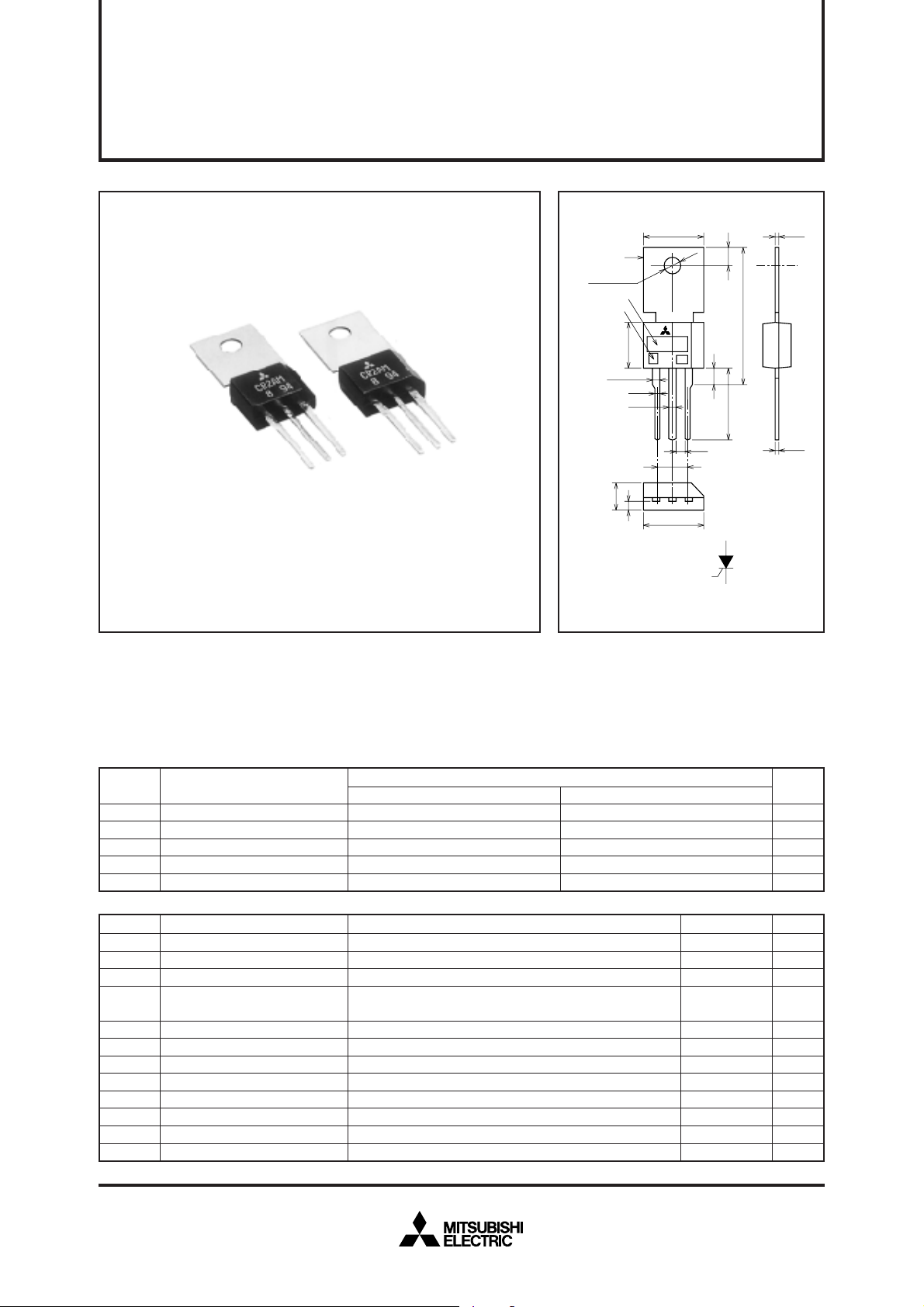
OUTLINE DRAWING
10 MAX
4
φ3.2±0.1
TYPE NAME
VOLTAGE
CLASS
@
∗
8 MAX
1.2±0.1
0.8
0.8
2.5 2.5
231
4.5 MAX
10 MAX
1.55±0.1
TO-202
Dimensions
3.2±0.2
23.7±0.5
4 MAX
12 MIN
1.5 MIN
Measurement point of
∗
case temperature
4
2
3
1
CATHODE
1
ANODE
2
GATE
3
ANODE
4
in mm
0.5
0.5
APPLICATION
Control of household equipment such as electric blandets, leakage protector, static switch, other
general purpose control applications, ignitors
MAXIMUM RATINGS
Conditions
Voltage class
c=75°C
12
600
720
480
600
480
Ratings
3.15
2.0
20
1.6
0.5
0.1
6
6
0.3
–40 ~ +125
–40 ~ +125
1.6
Symbol
RRM
V
VRSM
VR (DC)
VDRM
VD (DC)
Symbol
I
T (RMS)
IT (AV)
ITSM
2
t
I
PGM
PG (AV)
VFGM
VRGM
IFGM
Tj
Tstg
✽1. With Gate-to-cathode resistance RGK=1kΩ
Repetitive peak reverse voltage
Non-repetitive peak reverse voltage
DC reverse voltage
Repetitive peak off-state voltage
DC off-state voltage
RMS on-state current
Average on-state current
Surge on-state current
2
I
t
for fusing
Peak gate power dissipation
Average gate power dissipation
Peak gate forward voltage
Peak gate reverse voltage
Peak gate forward current
Junction temperature
Storage temperature
Weight
—
Parameter
Parameter
8
400
500
✽1
✽1
Commercial frequency, sine half wave, 180° conduction, T
60Hz sine half wave 1 full cycle, peak value, non-repetitive
Value corresponding to 1 cycle of half wave 60Hz, Surge on-state
current
Typical value
320
400
320
Unit
V
V
V
V
V
Unit
A
A
A
2
A
s
W
W
V
V
A
°C
°C
g
Feb.1999

MITSUBISHI SEMICONDUCTOR 〈THYRISTOR〉
NON-INSULATED TYPE, GLASS PASSIVATION TYPE
ELECTRICAL CHARACTERISTICS
Symbol
I
RRM
IDRM
VTM
VGT
VGD
IGT
Rth (j-c)
✽2.The method point for case temperature is at the anode tab 1.5mm away from the molded case.
✽3.If special values of I
The above values do not include the current flowing through the 1kΩ resistance between the gate and cathode.
Repetitive peak reverse current
Repetitive peak off-state current
On-state voltage
Gate trigger voltage
Gate non-trigger voltage
Gate trigger current
Thermal resistance
Item
I
GT (µA)
Parameter
j=125°C, VRRM applied
T
T
j=125°C, VDRM applied, RGK=1kΩ
T
c=25°C, ITM=4A, Instantaneous value
T
j=25°C, VD=6V, IT=0.1A
T
j=125°C, VD=1/2VDRM, RGK=1kΩ
T
j=25°C, VD=6V, IT=0.1A
Junction to case
GT are required, choose at least two items from those listed in the table below. (Example: AB, BC)
A
1 ~ 30
B
20 ~ 50
C
40 ~ 100
Test conditions
✽2
LOW POWER USE
Limits
Typ.
Min.
—
—
—
—
—
—
—
—
—
0.2
—
1
—
—
CR2AM
0.1
0.1
1.8
0.8
Unit
mA
mA
V
V
—
10
V
✽3
µA
°C/W
Max.
100
PERFORMANCE CURVES
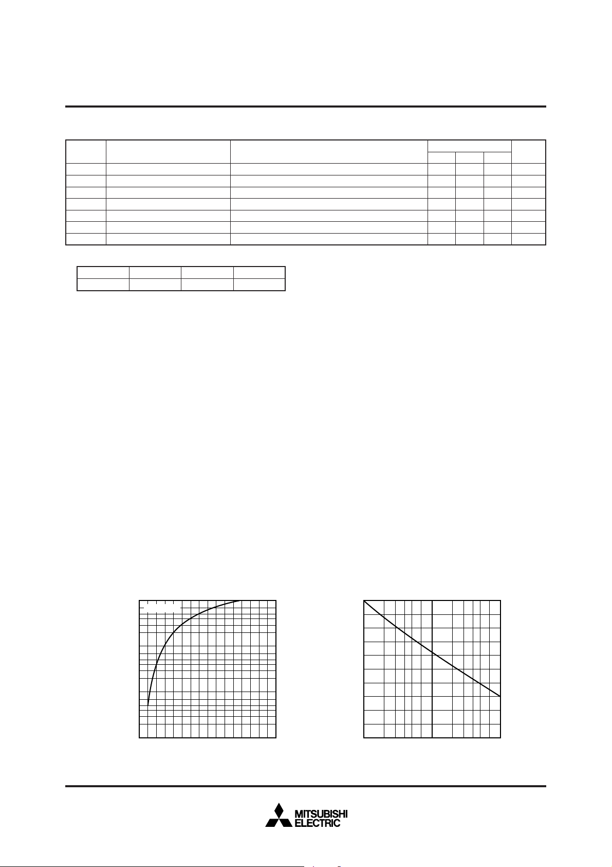
MAXIMUM ON-STATE CHARACTERISTICS
1
10
7
Tc = 25°C
5
3
2
0
10
7
5
3
2
–1
10
7
5
ON-STATE CURRENT (A)
3
2
–2
10
ON-STATE VOLTAGE (V)
RATED SURGE ON-STATE CURRENT
20
18
16
14
12
10
8
6
4
2
SURGE ON-STATE CURRENT (A)
3.80.6 1.4 2.2 3.01.0 1.8 2.6 3.4
0
10023 5710
44
1
23 5710
2
CONDUCTION TIME
(CYCLES AT 60Hz)
Feb.1999
 Loading...