

Page 1
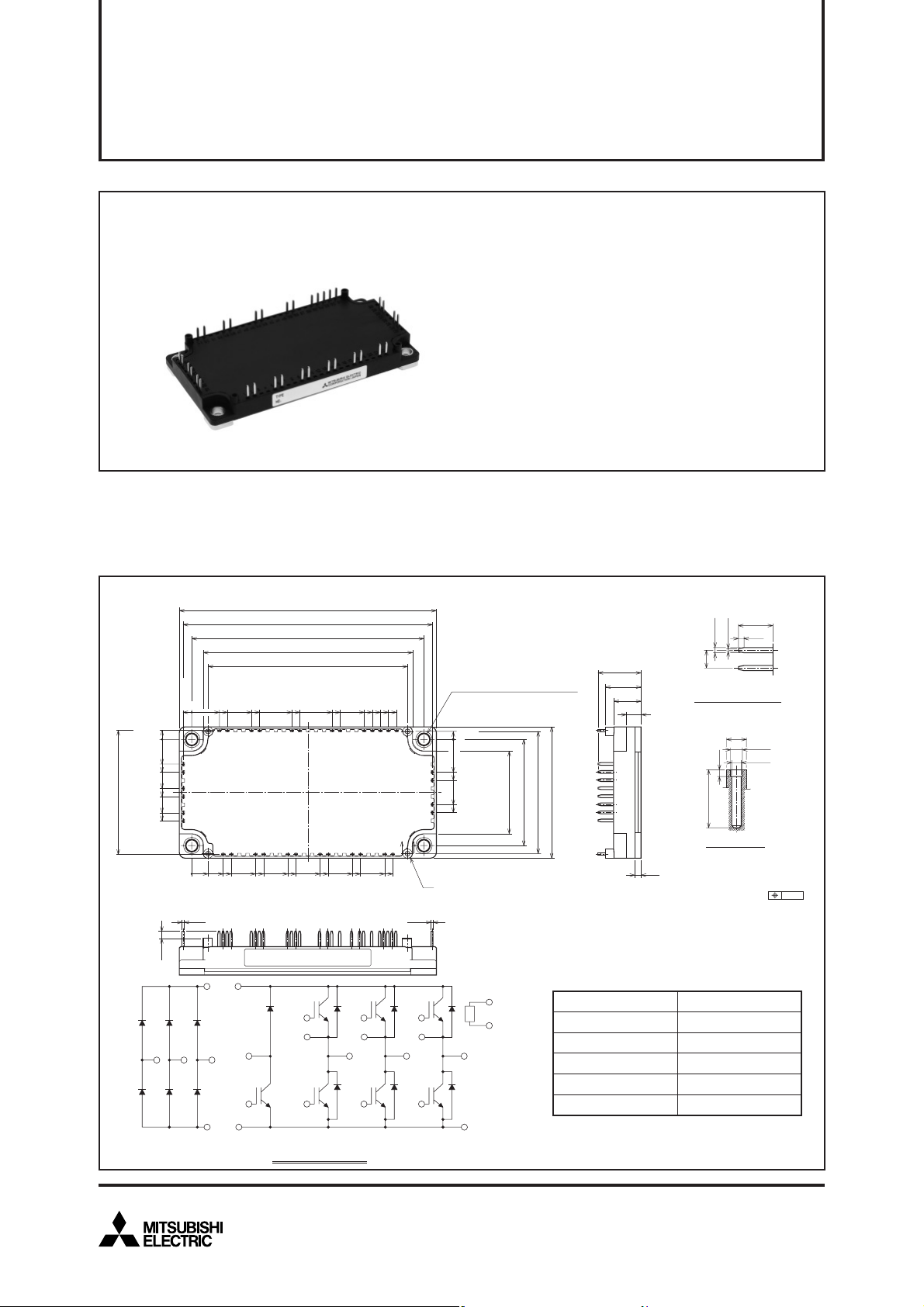
CM50MX-24A
MITSUBISHI IGBT MODULES
CM50MX-24A
HIGH POWER SWITCHING USE
C ..................................................................... 50A
¡I
CES ......................................................... 1200V
¡V
¡CIB (3-phase Converter +
3-phase Inverter + Brake)
¡Flatbase Type / Insulated Package /
Copper base plate
¡RoHS Directive compliant
APPLICATION
General purpose Inverters, Servo Amplifiers
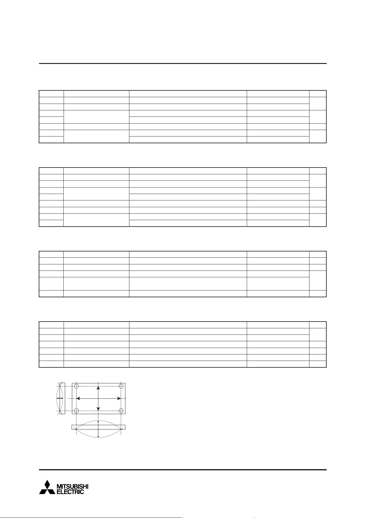
OUTLINE DRAWING & CIRCUIT DIAGRAM
0
*4.06
*13.09
*16.9
*4.2
0
*11.66
*15.48
*23.1
*26.9
*58.4
*34.52
*38.34
3.5
R(1~2) S(5~6) T(9~10)
* Use both terminals (R/S/T/P/N/P1/B/N1/U/V/W) to the external connection.
53
52 51 50 49 48 47 46 45 44 43 42 41 40 39 38 37 36 35 34 33 32 31
54
55
56
57
58
59
60
61
1
2 3 4 5 6 7 8 9 10 11 12 13 14 15 16 17 18 19 20 21 22
0
*15
(7.75)
*18.8
0.8
P(52~53) P1(54~55)
B(24~25)
GB(35)
N(57~58) N1(60~61)
121.7
*118.1
±0.5
110
99
94.5
*28.33
*32.14
*47.38
*51.19
*30.24
*34.04
*45.48
*49.28
LABEL
GuP(49)
EuP(48)
GuN(34)
CIRCUIT DIAGRAM
*66.43
*60.72
*64.52
*70.24
*75.96
*79.76
GvP(44)
EvP(43)
U(13~14)
GvN(33)
*81.67
*85.48
*89.29
*93.1
*96.91
*95
*91.2
0.8
GwP(39)
EwP(38)
V(17~18) W(21~22)
GwN(32)
30
29
28
27
26
25
24
23
A
4-φ5.5 MOUNTING HOLES
3.75
0
*15.48
*19.28
*30.72
*34.52
NTC
E(31)
TH1(29)
TH2(28)
±0.5
62
39
57.5
50
Toleranceotherwisespecified
20.5
17
13
7
(3)
Division of Dimension
0.5 to 3
over 3 to 6
over 6 to 30
over 30 to 120
over 120 to 400
Dimensions in mm
(7.4)
1.2
1.15
0.65
(3.81)
TERMINAL t = 0.8
φ4.3
φ2.5
φ2.1
1.5
12.5
SECTION A
*Pin positions
with tolerance
Tolerance
±0.2
±0.3
±0.5
±0.8
±1.2
φ0.5
Jan. 2009
Page 2
MITSUBISHI IGBT MODULES
CM50MX-24A
HIGH POWER SWITCHING USE
ABSOLUTE MAXIMUM RATINGS (Tj = 25°C, unless otherwise specified)
INVERTER PART
Symbol Parameter Conditions Rating Unit
CES
V
V
GES
I
C
I
CRM
P
C
I
E (Note.3)
I
ERM(Note.3)
Collector-emitter voltage
Gate-emitter voltage
Collector current
Maximum collector dissipation
Emitter current
(Free wheeling diode forward current)
BRAKE PART
Symbol Parameter Conditions
CES
V
V
GES
I
C
I
CRM
P
C
V
RRM(Note.3)
I
F (Note.3)
I
FRM(Note.3)
Collector-emitter voltage
Gate-emitter voltage
Collector current
Maximum collector dissipation
Repetitive peak reverse voltage
Forward current
G-E Short
C-E Short
DC, T
C
= 97°C
Pulse
T
C
= 25°C
T
C
= 25°C
Pulse
G-E Short
C-E Short
DC, T
C
= 106°C
Pulse
T
C
= 25°C
C
= 25°C
T
Pulse
(Note. 1)
(Note. 4)
(Note. 1, 5)
(Note. 1)
(Note. 4)
(Note. 1)
(Note. 4)
(Note. 1, 5)
(Note. 1)
(Note. 4)
1200
±20
50
100
355
50
100
Rating Unit
1200
±20
30
60
260
1200
30
60
V
A
W
A
V
A
W
V
A
CONVERTER PART
Symbol Parameter Conditions
V
E
I
O
I
FSM
I2t
RRM
a
Repetitive peak reverse voltage
Recommended AC input voltage
DC output current
Surge forward current
C
urrent square time
3-phase full wave rectifying, T
The sine half wave 1 cycle peak value, f = 60Hz,
non-repetitive
Value for one cycle of surge current
MODULE
Symbol Parameter Conditions
j
T
T
stg
V
iso
Note. 8: The base plate flatness measurement points are in the following figure.
Junction temperature
Storage temperature
Isolation voltage
—
Base plate flatness
—
Torque strength
—
Weight
+
–
Heatsinkside
Terminals to base plate, f = 60Hz, AC for 1 minute
On the centerline X, Y
Mounting M5 screw
(Typical)
Y
+:convex
–:concave
X
–
C
= 141°C
(Note. 1)
(Note. 8)
Rating Unit
1600
440
50
500
1040
Rating Unit
–40 ~ +150
–40 ~ +125
2500
±0 ~ +100
2.5 ~ 3.5
270
V
Vrms
A
2
A
°C
Vrms
μm
N·m
g
S
+
Heatsinkside
Jan. 2009
2
Page 3
MITSUBISHI IGBT MODULES
CM50MX-24A
HIGH POWER SWITCHING USE
ELECTRICAL CHARACTERISTICS (T
j
= 25°C, unless otherwise specified)
INVERTER PART
Symbol Parameter Conditions
I
CES
V
GE(th)
I
GES
V
CE(sat)
C
ies
C
oes
C
res
Q
G
t
d(on)
t
r
t
d(off)
t
f
t
rr (Note.3)
Q
rr (Note.3)
V
EC(Note.3)
R
th(j-c)Q
R
th(j-c)R
R
Gint
R
G
Collector cutoff current
Gate-emitter threshold voltage
Gate leakage current
Collector-emitter saturation
voltage
Input capacitance
Output capacitance
Reverse transfer capacitance
Total gate charge
Turn-on delay time
Turn-on rise time
Turn-off delay time
Turn-off fall time
Reverse recovery time
Reverse recovery charge
Emitter-collector voltage
Thermal resistance
(Junction to case)
(Note. 1)
Internal gate resistance
External gate resistance
V
CE
= V
CES
, VGE = 0V
I
C
= 5mA, VCE = 10V
±V
GE
= V
GES
, VCE = 0V
I
C
= 50A, VGE = 15V
C
= 50A, VGE = 15V
I
V
CE
= 10V
V
GE
= 0V
CC
= 600V, IC = 50A, VGE = 15V
V
V
CC
= 600V, IC = 50A
V
GE
= ±15V, RG = 6.2Ω
Inductive load
(I
E
= 50A)
E
= 50A, VGE = 0V
I
E
= 50A, VGE = 0V
I
per 1/6 IGBT
per 1/6 free wheeling diode
T
C
= 25°C, per switch
(Note. 6)
(Note. 6)
T
j
= 25°C
T
j
= 125°C
Chip
T
j
= 25°C
T
j
= 125°C
Chip
(Note. 6)
Limits
Min. Typ. Max.
—
6
—
—
—
—
—
—
—
—
—
—
—
—
—
—
—
—
—
—
—
—
6
—
7
—
2.0
2.2
1.9
—
—
—
250
—
—
—
—
—
2
2.6
2.16
2.5
—
—
0
—
1
8
0.5
2.6
—
—
8.5
0.75
0.17
—
100
50
300
600
200
—
3.4
—
—
0.35
0.63
—
62
Unit
mA
V
μA
V
nF
nC
ns
μC
V
K/W
Ω
BRAKE PART
Symbol Parameter Conditions
I
CES
VGE(th)
IGES
VCE(sat)
Cies
Coes
Cres
QG
I
RRM(Note.3)
VFM(Note.3)
Rth(j-c)Q
Rth(j-c)R
RGint
RG
Collector cutoff current
Gate-emitter threshold voltage
Gate leakage current
Collector-emitter saturation
voltage
Input capacitance
Output capacitance
Reverse transfer capacitance
Total gate charge
Repetitive peak reverse current
Forward voltage drop
Thermal resistance
(Junction to case)
(Note. 1)
Internal gate resistance
External gate resistance
V
CE = VCES, VGE = 0V
I
C = 3mA, VCE = 10V
±V
GE = VGES, VCE = 0V
I
C = 30A, VGE = 15V
C = 30A, VGE = 15V
I
V
CE = 10V
V
GE = 0V
CC = 600V, IC = 30A, VGE = 15V
V
V
R = VRRM
IF = 30A
F = 30A
I
per IGBT
per Clamp diode
T
C = 25°C
CONVERTER PART
Symbol Parameter Conditions
I
RRM
V
R
F
th(j-c)
Repetitive peak reverse current
Forward voltage drop
Thermal resistance
(Junction to case)
(Note. 1)
V
R
= V
RRM
I
F
= 50A
per Diode
, Tj = 150°C
(Note. 6)
(Note. 6)
T
j = 25°C
T
j = 125°C
Chip
T
j = 25°C
T
j = 125°C
Chip
(Note. 6)
Limits
Min. Typ. Max.
—
—
—
—
—
—
—
—
—
—
—
—
—
—
—
—
10
—
6
7
—
2.0
2.2
1.9
—
—
—
150
—
2.6
2.16
2.5
—
—
0
—
1
8
0.5
2.6
—
—
5.1
0.45
0.1
—
1
3.4
—
—
0.48
0.79
—
100
Limits
Min. Typ. Max.
—
—
—
—
1.2
—
6
1.6
0.33
Unit
mA
V
μA
V
nF
nC
mA
V
K/W
Ω
Unit
mA
V
K/W
Jan. 2009
3
Page 4

MITSUBISHI IGBT MODULES
CM50MX-24A
HIGH POWER SWITCHING USE
NTC THERMISTOR PART
Symbol Parameter Conditions
R
ΔR/R
B
(25/50)
P
25
Zero power resistance
Deviation of resistance
B constant
Power dissipation
T
C
= 25°C
T
C
= 100°C, R
100
= 493Ω
Approximate by equation
T
C
= 25°C
(Note. 7)
Min. Typ. Max.
4.85
–7.3
MODULE
Symbol Parameter Conditions
R
th(c-f)
Note.1: Case temperature (TC), heat sink temperature (Tf) measured point is just under the chips. (Refer to the figure of the chip location.)
Contact thermal resistance
(Case to fin)
2: Typical value is measured by using thermally conductive grease of λ = 0.9W/(m·K).
E, IERM, VEC, trr, Qrr and Err represent ratings and characteristics of the anti-parallel, emitter-collector free wheeling diode (FWDi).
3: I
I
F, IFRM, VF, VRRM and IRRM represent ratings and characteristics of the Clamp diode of Brake part.
4: Pulse width and repetition rate should be such that the device junction temperature (T
5: Junction temperature (T
6: Pulse width and repetition rate should be such as to cause negligible temperature rise.
(Refer to the figure of the test circuit for V
7:
B
(25/50)
R25: resistance at absolute temperature T
50
: resistance at absolute temperature T
R
25
1
R
= In( )/( )
T
R
50
25
(Note. 1)
j) should not increase beyond 150°C.
1
T
50
Thermal grease applied
per 1 module
CE(sat) and VEC)
25
[K]; T
25
= 25 [°C]+273.15 = 298.15 [K]
50
[K]; T
50
= 50 [°C]+273.15 = 323.15 [K]
(Note. 2)
j
) dose not exceed Tjmax rating.
Min. Typ. Max.
Limits
5.00
—
—
3375
—
—
Limits
0.015 ——K/W
5.15
+7.8
—
10
Unit
kΩ
%
K
mW
Unit
Chip Location (Top view) Dimensions in mm (tolerance: ±1mm)
(121.7)
(110)
0
0
54
55
56
57
58
59
60
61
0
(62)
(50)
27.4
28.4
42.0
Each mark points the center position of each chip. Tr**: IGBT, Di**: FWDi (DiBr: Clamp diode), CR**: Converter diode, Th: NTC thermistor
29.7
38.8
47.9
63.9
70.4
75.9
85.8
53
52 51 50 49 48 47 46 45 44 43 42 41 40 39 38 37 36 35 34 33 32 31
r
T
V
i
N
72.1
T
r
D
i
W
P
P
B
r
D
D
i
T
r
V
W
P
V
N
D
i
V
N
78.1
83.1
86.5
T
N
44.9
r
U
P
D
i
T
U
P
U
N
D
U
62.7
26.7
CTR
N
P
35.8
CRRNCSR
CRRPCSRPCTR
1
2 3 4 5 6 7 8 9 10 11 12 13 14 15 16 17 18 19 20 21 22
91.3
r
P
T
i
93.5
h
D
W
97.6
T
B
T
W
N
i
N
99.4
101.2
r
r
r
102.8
30
29
28
27
26
25
24
23
LABEL SIDE
0
18.6
26.7 (Tr/UP, Tr/VP, Tr/WP)
27.4 (Di/Br)
27.9 (Th)
34.9 (Di/UP, Di/VP, Di/WP)
35.6 (Tr/UN, Tr/VN, Tr/WN)
43.3
Jan. 2009
4
Page 5
MITSUBISHI IGBT MODULES
CM50MX-24A
HIGH POWER SWITCHING USE
P1
VGE = 15V
V
GuP
EuP
U
GE
= 0V
V
GuN
E
N1
P side Inverter part T
r
(example of U arm)
G*E*
= 0V
V
(GvP-EvP, GwP-EwP, GvN-E, GwN-E, GB-E)
P1
VGE = 0V
V
GuP
EuP
U
P1
GE
= 0V
V
I
C
GuP
EuP
U
VGE = 15V
GuN
E
N1
N side Inverter part T
(example of U arm)
G*E*
= 0V
V
(GvP-EvP, GwP-EwP, GvN-E, GwN-E, GB-E)
V
CE(sat)
test circuit
P1
GE
= 0V
V
I
E
GuP
EuP
U
P1
B
VGE = 15V
V
I
C
r
GB
E
V
B
G*E*
N1
r Tr
= 0V
V
I
C
(GuP-EuP, GvP-EvP, GwP-EwP,
GuN-E, GvN-E, GwN-E)
P1
V
I
F
B
GE
= 0V
V
GuN
E
N1
P side Inverter part D
i
(example of U arm)
G*E*
= 0V
V
(GvP-EvP, GwP-EwP, GvN-E, GwN-E, GB-E)
I
Load
V
CE
E
C
I
0V
+V
–V
Arm
–V
GE
GE
R
G
V
GE
GE
Switching time test circuit and waveforms
VGE = 0V
GuN
E
N1
N side Inverter part D
V
I
E
i
(example of U arm)
G*E*
= 0V
V
(GvP-EvP, GwP-EwP, GvN-E, GwN-E, GB-E)
EC/VFM
test circuit
V
V
GE
0V
VCC+
I
C
0A
t
d(on)
t
r
t
d(off)
90%
0%
90%
t
f
I
10%
E
0A
VGE = 0V
GB
E
N1
r Di
B
V
G*E*
= 0V
(GuP-EuP, GvP-EvP, GwP-EwP,
GuN-E, GvN-E, GwN-E)
t
rr
1/2 ✕ I
Q
rr
= 1/2 ✕ Irr ✕ t
rr
I
rr
t
rr, Qrr
test waveform
t
rr
Jan. 2009
5
Page 6

PERFORMANCE CURVES
OUTPUT CHARACTERISTICS
100
V
GE
90
20V
(A)
80
C
70
60
50
40
30
20
COLLECTOR CURRENT I
10
0
(TYPICAL) Inverter part
=
15
Tj = 25°C
13
12
11
10
246813579
MITSUBISHI IGBT MODULES
CM50MX-24A
HIGH POWER SWITCHING USE
COLLECTOR-EMITTER SATURATION
VOLTAGE CHARACTERISTICS
4
(V)
3.5
CE(sat)
3
2.5
2
1.5
1
COLLECTOR-EMITTER
9
100
0.5
SATURATION VOLTAGE V
0
(TYPICAL) Inverter part
V
GE
= 15V
0
20 40 60 80 100
Tj = 25°C
T
j
= 125°C
COLLECTOR-EMITTER VOLTAGE VCE (V)
COLLECTOR-EMITTER SATURATION
VOLTAGE CHARACTERISTICS
(TYPICAL) Inverter part
10
Tj = 25°C
(V)
8
CE(sat)
6
4
COLLECTOR-EMITTER
2
SATURATION VOLTAGE V
0
GATE-EMITTER VOLTAGE VGE (V)
CAPACITANCE CHARACTERISTICS
2
10
7
5
3
2
1
10
7
5
3
2
0
10
7
5
3
2
–1
CAPACITANCE (nF)
10
7
5
3
2
–2
10
10
(TYPICAL) Inverter part
V
GE
= 0V
–1
2
0
10
357 2
357 2
10
1
IC = 100A
IC = 50A
IC = 20A
C
ies
C
oes
C
res
357
206 8 10 12 14 16 18
10
COLLECTOR CURRENT I
C
(A)
FREE WHEELING DIODE
FORWARD CHARACTERISTICS
(TYPICAL) Inverter part
3
10
7
5
3
(A)
2
E
2
10
7
5
3
2
1
10
7
5
EMITTER CURRENT I
3
2
0
10
0 0.5 1 1.5 2 3 3.5 4
EMITTER-COLLECTOR VOLTAGE V
2.5
Tj = 25°C
T
j
= 125°C
EC
(V)
HALF-BRIDGE
SWITCHING CHARACTERISTICS
(TYPICAL) Inverter part
3
10
7
5
3
2
2
10
7
5
3
2
Conditions:
1
10
V
CC
= 600V
7
V
GE
= ±15V
5
SWITCHING TIME (ns)
R
G
= 6.2Ω
3
T
j
= 125°C
2
Inductive load
0
10
2
10
0
23 57
10
1
23 57
t
f
t
d(off)
t
d(on)
t
r
10
2
COLLECTOR-EMITTER VOLTAGE VCE (V)
COLLECTOR CURRENT I
C
(A)
Jan. 2009
6
Page 7

MITSUBISHI IGBT MODULES
CM50MX-24A
HIGH POWER SWITCHING USE
SWITCHING CHARACTERISTICS
HALF-BRIDGE
3
10
7
5
3
2
2
10
7
5
3
2
1
10
7
5
SWITCHING TIME (ns)
3
2
0
10
10
(TYPICAL) Inverter part
t
f
t
d(off)
t
d(on)
t
r
0
57
10
1
GATE RESISTANCE R
HALF-BRIDGE
SWITCHING CHARACTERISTICS
(TYPICAL) Inverter part
2
10
Conditions:
7
V
CC
= 600V
5
V
GE
= ±15V
I
C
, IE = 50A
3
T
j
= 125°C
2
Inductive load
1
10
7
5
3
2
SWITCHING LOSS (mJ/pulse)
0
10
0
10
10
0
57
10
1
Conditions:
V
CC
= 600V
V
GE
= ±15V
I
C
= 50A
T
j
= 125°C
Inductive load
23 5723
G
(Ω)
E
E
E
23 5723
SWITCHING CHARACTERISTICS
HALF-BRIDGE
(TYPICAL) Inverter part
1
10
7
5
3
2
E
off
E
rr
E
on
Conditions:
V
CC
= 600V
V
GE
= ±15V
R
G
= 6.2Ω
T
j
= 125°C
Inductive load
1
10
57
23 5723
COLLECTOR CURRENT I
EMITTER CURRENT I
2
10
C
(A)
E
(A)
10
0
10
7
5
3
2
SWITCHING LOSS (mJ/pulse) l
–1
10
2
10
0
REVERSE RECOVERY CHARACTERISTICS
OF FREE WHEELING DIODE
3
10
7
5
3
2
(ns)
rr
(A), t
rr
10
10
10
2
7
5
3
2
1
7
5
3
2
0
10
10
on
off
rr
2
10
(TYPICAL) Inverter part
0
0
57
10
1
t
rr
I
rr
Conditions:
V
CC
= 600V
V
GE
= ±15V
R
G
= 6.2Ω
T
j
= 25°C
Inductive load
23 5723
10
2
GATE RESISTANCE R
GATE CHARGE CHARACTERISTICS
(TYPICAL) Inverter part
20
IC = 50A
(V)
GE
VCC = 400V
15
10
5
GATE-EMITTER VOLTAGE V
0
0 50 100 150 200 250 300 350
GATE CHARGE QG (nC)
G
(Ω)
VCC = 600V
0
10
7
5
3
th(j–c)
2
–1
10
7
5
3
2
–2
10
7
5
NORMALIZED TRANSIENT
3
THERMAL IMPEDANCE Z
2
–3
10
10
7
EMITTER CURRENT I
E
(A)
TRANSIENT THERMAL
IMPEDANCE CHARACTERISTICS
Single pulse,
T
C
= 25°C
Inverter IGBT part : Per unit base = R
Inverter FWDi part : Per unit base = R
Converter-Di part : Per unit base = R
Brake IGBT part : Per unit base = R
Brake Clamp-Di part : Per unit base = R
–5
–4
10
23 57
10
–3
23 57
23 57
10
–2
23 57
10
th(j–c)
th(j–c)
th(j–c)
th(j–c)
th(j–c)
–1
23 57
= 0.35K/W
= 0.63K/W
= 0.33K/W
= 0.48K/W
= 0.79K/W
TIME (s)
10
0
23 57
1
10
Jan. 2009
Page 8

MITSUBISHI IGBT MODULES
CM50MX-24A
HIGH POWER SWITCHING USE
RECTIFIER DIODE
FORWARD CHARACTERISTICS
(TYPICAL) Converter part
2
10
7
5
3
2
1
10
7
5
3
FORWARD CURRENT lF (A)
2
0
10
0 0.5 1.0 1.5 2.0
FORWARD VOLTAGE V
CLAMP DIODE
FORWARD CHARACTERISTICS
(TYPICAL) Brake part
2
10
7
5
(A)
F
3
2
Tj = 25°C
T
j
= 125°C
F (V)
COLLECTOR-EMITTER SATURATION
VOLTAGE CHARACTERISTICS
(TYPICAL) Brake part
4
V
GE
= 15V
3.5
3
2.5
2
1.5
1
COLLECTOR-EMITTER
0.5
SATURATION VOLTAGE VCE(sat) (V)
0
0
10 20 30 40 50 60
COLLECTOR CURRENT I
Tj = 25°C
T
j
= 125°C
C (A)
1
10
7
5
3
2
FORWARD CURRENT I
0
10
0 0.5 1 1.5 2 2.5 3 3.5 4 4.5 5
FORWARD VOLTAGE VF (V)
Tj = 25°C
T
j
= 125°C
Jan. 2009
8
 Loading...