

Page 1
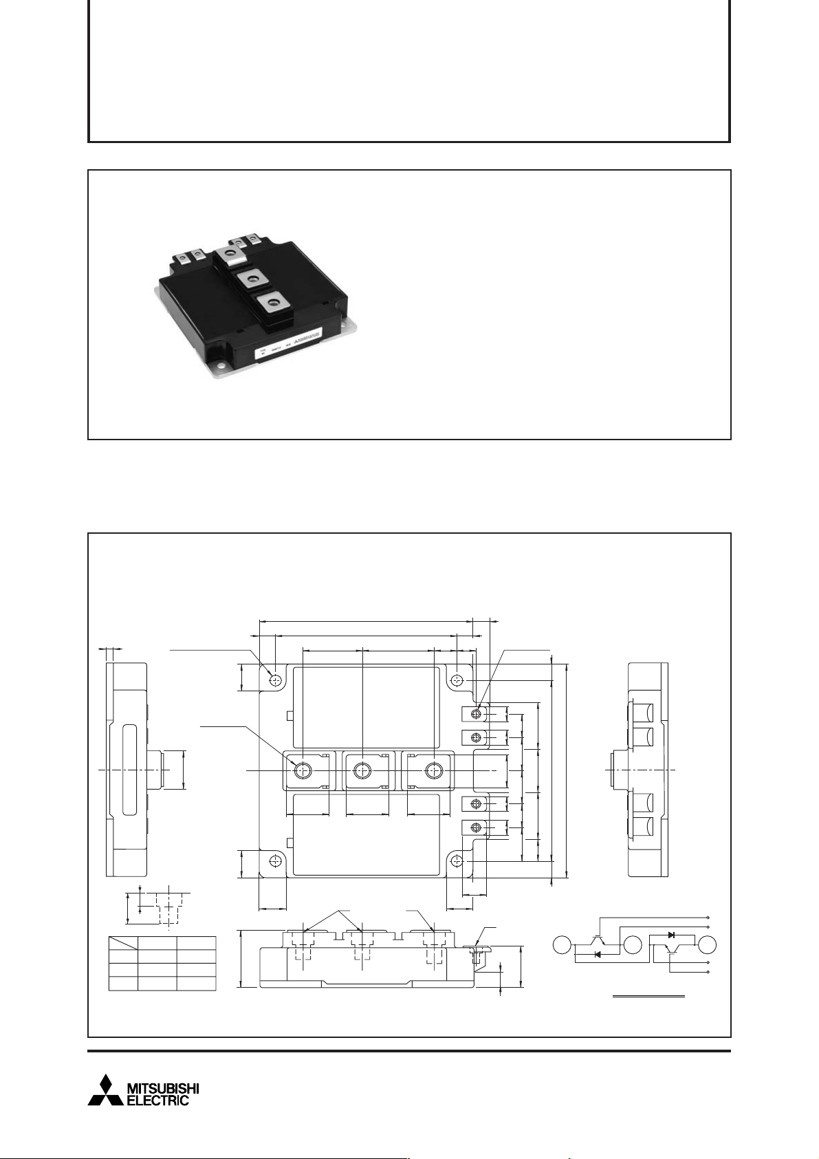
CM400DY-34A
MITSUBISHI IGBT MODULES
CM400DY-34A
HIGH POWER SWITCHING USE
¡IC ...................................................................400A
¡V
CES ......................................................... 1700V
¡Insulated Type
¡2-elements in a pack
APPLICATION
General purpose inverters & Servo controls, etc
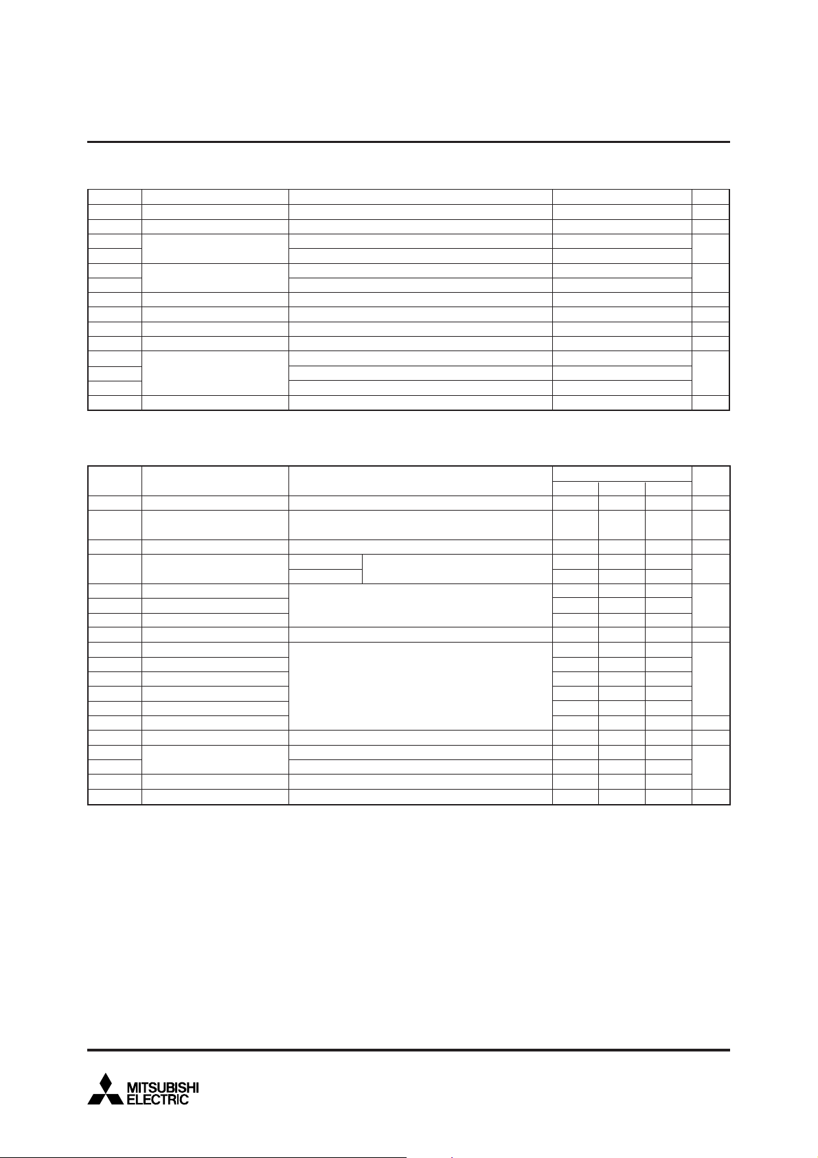
OUTLINE DRAWING & CIRCUIT DIAGRAM Dimensions in mm
13.8
16.5
1010
11.5
G2G1 E2E1
(15)
10
C
9.1
4-M4NUTS
14.5
20
9 9 9 9
20.5 14.5 20 20
13.5 28.5 28.526
+1
–0.5
24.5
10
±0.2
110
10
C2E1
130
E2
CIRCUIT DIAGRAM
130
±0.2
4
LABEL
L
A
B
C
M
L
16
19
10
4-φ6.5
(
MOUNTINGHOLES
3-M8NUTS
24
M
7
7
3.5
)
16.5
(26) (26) (26)
16.5
16.5
+1
–0.5
35
110
36 43.8
E2
C2E1
AB
C1
E2 G2G1 E1
C1
Jun. 2007
Page 2
ABSOLUTE MAXIMUM RATINGS (Tj = 25°C, unless otherwise specified)
Symbol Parameter
V
CES
VGES
IC
ICM
IE (
IEM (
PC (
Tj
Tstg
Viso
Collector-emitter voltage
Gate-emitter voltage
Collector current
Note 1
)
Emitter current
Note 1
)
Maximum collector dissipation
Note 3
)
Junction temperature
Storage temperature
Isolation voltage
—
Torque strength
—
—
—
Weight
G-E Short
C-E Short
DC, T
C = 107°C
Pulse (Note 2)
Operation (Note 2)
Pulse (Note 2)
C = 25°C
*1
T
Main terminal to base plate, AC 1 min.
Main terminal M8
Mounting holes M6
G(E) terminal M4
Typical value
Conditions UnitRatings
*1
MITSUBISHI IGBT MODULES
CM400DY-34A
HIGH POWER SWITCHING USE
1700
±20
(Note 2)
400
800
400
800
3780
–40 ~ +150
–40 ~ +125
3500
8.8 ~ 10.8
3.5 ~ 4.5
1.3 ~ 1.7
1200
V
V
A
A
W
°C
°C
V
N • m
g
ELECTRICAL CHARACTERISTICS (Tj = 25°C, unless otherwise specified)
Symbol
ICES
V
GE(th)
IGES
VCE(sat)
Cies
Coes
Cres
QG
td(on)
tr
td(off)
tf
trr (
Qrr (
VEC(
Rth(j-c)Q
th(j-c)R
R
th(c-f)
R
RG
1 : Tc, Tf measured point is just under the chips.
*
2 : Typical value is measured by using Shin-Etsu Chemical Co.,Ltd “G-746”.
*
Note 1. I
Collector cutoff current
Gate-emitter threshold
voltage
Gate leakage current
Collector to emitter saturation
voltage
Input capacitance
Output capacitance
Reverse transfer capacitance
Total gate charge
Turn-on delay time
Turn-on rise time
Turn-off delay time
Turn-off fall time
Reverse recovery time
Note 1
)
Reverse recovery charge
Note 1
)
Emitter-collector voltage
Note 1
)
Thermal resistance
Contact thermal resistance
External gate resistance
E, IEM, VEC, trr & Qrr represent characteristics of the anti-parallel, emitter to collector free-wheel diode (FWDi).
2. Pulse width and repetition rate should be such that the device junction temperature (T
3. Junction temperature (T
4. Pulse width and repetition rate should be such as to cause negligible temperature rise.
Parameter
VCE = VCES, VGE = 0V
I
C = 40mA, VCE = 10V
±V
T
j = 25°C
T
j = 125°C
CE = 10V
V
V
GE = 0V
CC = 1000V, IC = 400A, VGE = 15V
V
CC = 1000V, IC = 400A
V
V
GE1 = VGE2 = 15V
R
G = 1.2Ω, Inductive load switching operation
I
E = 400A
E = 400A, VGE = 0V
I
IGBT part (1/2 module)
FWDi part (1/2 module)
Case to fin, Thermal compound applied (1/2 module)
j) should not increase beyond 150°C.
GE = VGES, VCE = 0V
Test conditions
I
C = 400A, VGE = 15V
*1
*1
j) does not exceed Tjmax rating.
Min. Max.
—
5.5 8.5
—
—
—
—
—
—
—
—
—
—
—
—
—
—
—
—
*1,*2
—
1.2
Limits
Typ.
—
1
7.0 V
—
2.2
2.45
—
—
—
2670
—
—
—
—
—
40
—
—
—
0.019
—
2.0
2.8
—
98.8
11.2
2.12
—
950
300
1000
350
450
—
3.0
0.033
0.055
—
12
Unit
mA
µA
V
nF
nC
ns
µC
V
°C/W
Ω
Jun. 2007
2
Page 3

PERFORMANCE CURVES
MITSUBISHI IGBT MODULES
CM400DY-34A
HIGH POWER SWITCHING USE
OUTPUT CHARACTERISTICS
800
(A)
C
700
600
500
Tj = 25°C
V
GE
20V
=
15
13
12
11
400
300
200
100
COLLECTOR CURRENT I
0
2
046810
COLLECTOR-EMITTER VOLTAGE V
10
9
8
CE
(V)
COLLECTOR-EMITTER SATURATION
VOLTAGE CHARACTERISTICS
5
V
GE
(V)
CE (sat)
= 15V
4
3
2
TRANSFER CHARACTERISTICS
800
V
CE
)
700
A
(
C
600
= 10V
500
400
300
200
100
COLLECTOR CURRENT I
0
048121620
Tj = 25°C
T
j
= 125°C
GATE-EMITTER VOLTAGE VGE (V
COLLECTOR-EMITTER SATURATION
VOLTAGE CHARACTERISTICS
(V)
CE (sat)
10
8
6
4
Tj = 25°C
IC = 800A
IC = 400A
)
COLLECTOR-EMITTER
1
SATURATION VOLTAGE V
0
0 200 400 600 800
COLLECTOR CURRENT IC (A)
FREE-WHEEL DIODE
FORWARD CHARACTERISTICS
4
10
7
5
3
(A)
2
E
3
10
7
5
3
2
2
10
7
5
EMITTER CURRENT I
3
2
1
10
0.5 1 1.5 2 2.5 3 3.5 4
Tj = 25°C
T
j
= 125°C
EMITTER-COLLECTOR VOLTAGE V
Tj = 25°C
T
j
= 125°C
EC
(V)
COLLECTOR-EMITTER
2
SATURATION VOLTAGE V
0
0
4 8 12 16 20
GATE-EMITTER VOLTAGE V
CAPACITANCE–V
3
10
7
5
(nF)
3
2
res
2
10
, C
7
5
oes
3
, C
2
ies
1
10
7
5
3
2
0
10
7
5
3
2
CAPACITANCE C
–1
10
10
CHARACTERISTICS
V
GE
= 0V
–1
2
357 2
10
0
COLLECTOR-EMITTER VOLTAGE V
IC = 160A
CE
1
10
357 2
GE
(V)
C
ies
C
oes
C
res
357
CE
10
2
(V)
Jun. 2007
3
Page 4

MITSUBISHI IGBT MODULES
CM400DY-34A
HIGH POWER SWITCHING USE
SWITCHING CHARACTERISTICS
HALF-BRIDGE
SWITCHING TIME vs. COLLECTOR CURRENT
4
10
7
(ns)
5
f
, t
3
2
d(off)
, t
r
10
, t
d(on)
10
SWITCHING TIME t
10
3
7
5
3
2
7
5
3
2
10
t
d(off)
t
d(on)
t
f
10
2
Conditions:
CC
= 1000V
V
GE
= ±15V
V
G
= 1.2Ω
R
j
= 125°C
T
Inductive load
23 5723
2
1
1
t
r
57
COLLECTOR CURRENT IC (A)
SWITCHING LOSS vs.
COLLECTOR CURRENT
3
10
7
5
3
(mJ/pulse)
off
2
, E
on
2
10
7
5
3
2
SWITCHING LOSS E
1
10
1
10
57
10
2
E
rr
E
on
E
off
Conditions:
CC
= 1000V
V
GE
= ±15V
V
G
= 1.2Ω
R
j
= 125°C
T
Inductive load
23 5723
10
10
3
2
10
7
5
3
(mJ/pulse)
2
rr
1
10
7
5
3
2
SWITCHING LOSS E
0
10
3
SWITCHING CHARACTERISTICS
HALF-BRIDGE
SWITCHING TIME vs. GATE RESISTANCE
4
10
7
(ns)
5
f
, t
3
2
d(off)
, t
3
r
10
, t
7
5
d(on)
3
2
2
10
7
5
3
2
SWITCHING TIME t
1
10
0
10
57
10
t
t
1
t
d(on)
t
d(off)
r
f
Conditions:
CC
= 1000V
V
GE
= ±15V
V
C
= 400A
I
j
= 125°C
T
Inductive load
23 5723
GATE RESISTANCE RG (Ω)
SWITCHING LOSS vs.
3
10
7
5
3
(mJ/pulse)
off
2
, E
on
2
10
7
5
3
2
SWITCHING LOSS E
1
10
10
GATE RESISTANCE
0
57
10
E
E
E
1
rr
on
off
Conditions:
CC
= 1000V
V
V
GE
= ±15V
C
= 400A
I
j
= 125°C
T
Inductive load
23 5723
10
10
2
2
10
7
5
3
(mJ/pulse)
2
rr
1
10
7
5
3
2
SWITCHING LOSS E
0
10
2
COLLECTOR CURRENT I
REVERSE RECOVERY CHARACTERISTICS
OF FREE-WHEEL DIODE
3
10
(A)
rr
7
(ns)
rr
5
3
2
2
10
7
5
3
2
REVERSE RECOVERY TIME t
1
10
REVERSE RECOVERY CURRENT l
10
1
23 57
t
rr
I
rr
Conditions:
V
V
R
T
Inductive load
2
10
23 57
EMITTER CURRENT I
C
CC
= 1000V
GE
= ±15V
G
= 1.2Ω
j
= 25°C
C
(A)
(A)
10
GATE RESISTANCE R
G
(Ω)
TRANSIENT THERMAL
IMPEDANCE CHARACTERISTICS
(IGBT part & FWDi part)
0
10
7
5
(ratio)
3
2
th (j–c)
–1
10
7
5
3
2
–2
10
7
IGBT part:
5
NORMALIZED TRANSIENT
3
Per unit base = R
3
FWDi part:
2
Per unit base = R
THERMAL IMPEDANCE Z
–3
10
–5
–4
23 57
23 57
10
10
Single Pulse
Tc= 25°C
Tc measured point is
just under the chips
th(j–c)
= 0.033°C/W
th(j–c)
= 0.055°C/W
–3
–2
23 57
10
23 57
10
10
–1
23 57
10
0
23 57
10
1
TIME (s)
Jun. 2007
4
Page 5

20
16
MITSUBISHI IGBT MODULES
CM400DY-34A
HIGH POWER SWITCHING USE
GATE CHARGE
CHARACTERISTICS
IC = 400A
VCC = 800V
GATE-EMITTER VOLTAGE VGE (V)
12
VCC = 1000V
8
4
0
0
1000 2000 3000 4000
GATE CHARGE QG (nC)
Jun. 2007
5
 Loading...