

Page 1
CM400DX-12A
MITSUBISHI IGBT MODULES
CM400DX-12A
HIGH POWER SWITCHING USE
¡IC ...................................................................400A
CES ............................................................ 600V
¡V
¡Dual
¡Flatbase Type / Insulated Package /
Copper (non-plating) base plate
¡RoHS Directive compliant
APPLICATION
General purpose Inverters, Servo Amplifiers, Power supply, etc.
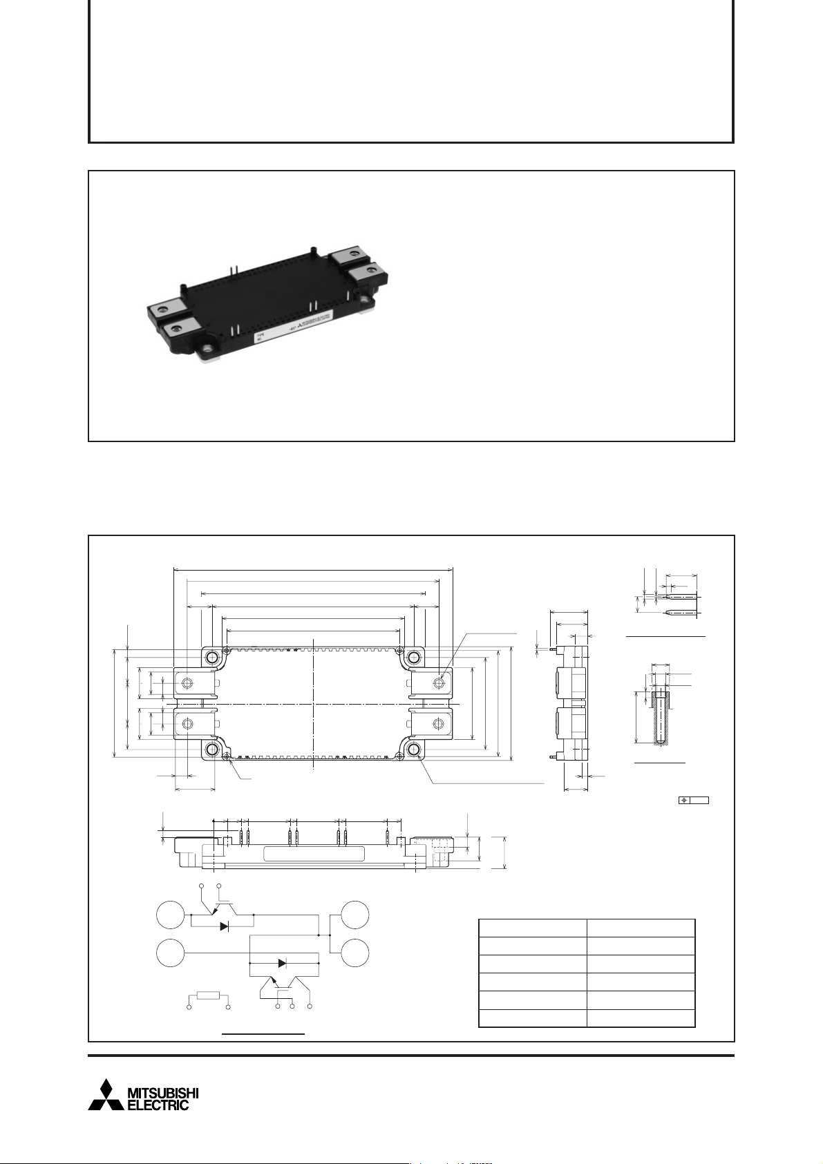
OUTLINE DRAWING & CIRCUIT DIAGRAM
152
137
Di1
Tr1
E1(16)
121.7
±0.5
110
99
94.5
*45.48
*41.66
LABEL
C1(22)G1(15)
*72.14
*68.34
E1C2
(24)
E1C2
(23)
4-M6 NUTS
24
±0.5
62
39
57.5
23
22
212019181716151413121110987654321
4-φ5.5 MOUNTING HOLES
(102.25)
*95
50
(5.4)
+1
-0.5
12.5
17
(SCREWING DEPTH)
Toleranceotherwisespecified
Division of Dimension
0.5 to 3
over 3 to 6
over 6 to 30
over 30 to 120
over 120 to 400
*58.4
22
(14) (14) (4.2)
(13.5) (13.5)
46
45 44 43 42 41 40 39 38 37 36 35 34 33 32 31 30 29 28 27 26 25
17
12
66
12
17
6.5
(21.14)
3.5
E2(47)
C1(48)
TH1(1)
47
48
0
E2(39) G2(38)
Th
NTC
TH2(2)
CIRCUIT DIAGRAM
(7.75)
Di2
A
*18.8
*15
Tr2
0.8
(20.5)
17
7
13
(3)
*Pin positions
with tolerance
Tolerance
Dimensions in mm
(7.4)
1.2
1.15
0.65
(3.81)
TERMINAL t = 0.8
φ4.3
φ2.5
φ2.1
1.5
12.5
SECTION A
±0.2
±0.3
±0.5
±0.8
±1.2
φ0.5
Jan. 2009
Page 2
MITSUBISHI IGBT MODULES
CM400DX-12A
HIGH POWER SWITCHING USE
ABSOLUTE MAXIMUM RATINGS (T
j
= 25°C, unless otherwise specified)
INVERTER PART
Symbol Parameter Conditions Rating Unit
CES
V
V
GES
I
C
I
CRM
P
C
I
E (Note.3)
I
ERM(Note.3)
T
j
T
stg
V
iso
Note. 8: The base plate flatness measurement points are in the following figure.
Collector-emitter voltage
Gate-emitter voltage
Collector current
Maximum collector dissipation
Emitter current
(Free wheeling diode forward current)
Junction temperature
Storage temperature
Isolation voltage
—
Base plate flatness
—
Torque strength
—
Torque strength
—
Weight
Y
+
–
X
Heatsinkside
–
G-E Short
C-E Short
DC, T
C
= 60°C
Pulse
T
C
= 25°C
T
C
= 25°C
Pulse
Terminals to base plate, f = 60Hz, AC 1 minute
On the centerilne X, Y
Main terminals M6 screw
Mounting M5 screw
(Typical)
+:convex
–:concave
(Note. 1)
(Note. 4)
(Note. 1, 5)
(Note. 1)
(Note. 4)
(Note. 8)
600
±20
400
800
1340
400
800
–40 ~ +150
–40 ~ +125
2500
±0 ~ +100
3.5 ~ 4.5
2.5 ~ 3.5
330
V
A
W
A
°C
Vrms
μm
N·m
g
+
Heatsinkside
Jan. 2009
2
Page 3
ELECTRICAL CHARACTERISTICS (Tj = 25°C, unless otherwise specified)
INVERTER PART
Symbol Parameter Conditions
I
CES
V
GE(th)
I
GES
V
CE(sat)
C
ies
C
oes
C
res
Q
G
t
d(on)
t
r
t
d(off)
t
f
t
rr (Note.3)
Q
rr (Note.3)
V
EC(Note.3)
R
lead
R
th(j-c)Q
R
th(j-c)R
R
th(c-f)
R
Gint
R
G
Collector cutoff current
Gate-emitter threshold voltage
Gate leakage current
Collector-emitter saturation voltage
Input capacitance
Output capacitance
Reverse transfer capacitance
Total gate charge
Turn-on delay time
Turn-on rise time
Turn-off delay time
Turn-off fall time
Reverse recovery time
Reverse recovery charge
Emitter-collector voltage
Module lead resistance
Thermal resistance
(Junction to case)
(Note. 1)
Contact thermal resistance
(Case to heat sink)
(Note. 1)
Internal gate resistance
External gate resistance
V
CE
= V
CES
, VGE = 0V
I
C
= 40mA, VCE = 10V
±V
GE
= V
GES
, VCE = 0V
I
C
= 400A, VGE = 15V
C
= 400A, VGE = 15V
I
V
CE
= 10V
V
GE
= 0V
CC
= 300V, IC = 400A, VGE = 15V
V
V
CC
= 300V, IC = 400A
V
GE
= ±15V, RG = 3.6Ω
Inductive load
E
= 400A)
(I
E
= 400A, VGE = 0V
I
E
= 400A, VGE = 0V
I
Main terminals-chip, per switch
per IGBT
per free wheeling diode
Thermal grease applied
per 1 module
T
C
= 25°C
(Note. 6)
(Note. 6)
T
j
= 25°C
T
j
= 125°C
Chip
j
= 25°C
T
T
j
= 125°C
Chip
MITSUBISHI IGBT MODULES
CM400DX-12A
HIGH POWER SWITCHING USE
Limits
Min. Typ. Max.
(Note. 6)
(Note. 2)
—
5
—
—
—
—
—
—
—
—
—
—
—
—
—
—
—
—
—
—
—
—
—
—
1.6
—
6
—
1.7
1.9
1.6
—
—
—
1100
—
—
—
—
—
2.0
1.95
1.9
1.1
—
—
0.015
0
—
0.5
2.1
—
—
50
5.3
1.6
—
200
200
400
600
200
—
2.8
—
—
—
0.093
0.16
—
—
16
Unit
mA
1
7
V
μA
V
nF
nC
ns
μC
V
mΩ
K/W
Ω
NTC THERMISTOR PART
Symbol Parameter Conditions
R
ΔR/R
B
(25/50)
P
25
Note.1: Case temperature (TC), heat sink temperature (Tf) measured point is just under the chips. (Refer to the figure of the chip location.)
Zero power resistance
Deviation of resistance
B constant
Power dissipation
2: Typical value is measured by using thermally conductive grease of λ = 0.9W/(m·K).
E, IERM, VEC, trr and Qrr represent ratings and characteristics of the anti-parallel, emitter-collector free wheeling diode (FWDi).
3: I
4: Pulse width and repetition rate should be such that the device junction temperature (T
5: Junction temperature (T
6: Pulse width and repetition rate should be such as to cause negligible temperature rise.
(Refer to the figure of the test circuit for V
7:
B
(25/50)
R25: resistance at absolute temperature T
50
: resistance at absolute temperature T
R
25
R
= In( )/( )
R
50
j) should not increase beyond 150°C.
1
1
T
T
25
50
T
C
= 25°C
T
C
= 100°C, R
100
= 493Ω
Approximate by equation
T
C
= 25°C
CE(sat) and VEC)
25
[K]; T
25
= 25 [°C]+273.15 = 298.15 [K]
50
[K]; T
50
= 50 [°C]+273.15 = 323.15 [K]
(Note. 7)
j) dose not exceed Tjmax rating.
Min. Typ. Max.
4.85
–7.3
Limits
5.00
—
—
3375
—
—
5.15
+7.8
—
10
Unit
kΩ
%
K
mW
Jan. 2009
3
Page 4

MITSUBISHI IGBT MODULES
CM400DX-12A
HIGH POWER SWITCHING USE
Chip Location (Top view) Dimensions in mm (tolerance: ±1mm)
(152)
(121.7)
(110)
(62)
(50)
0
21.5
32.0
0
46
45 44 43 42 41 40 39 38 37 36 35 34 33 32 31 30 29 28 27 26 25
47
Di2
TrTh2
48
29.6
36.3
43.2
Di1
Tr1
78.6
212019181716151413121110987654321
22
24
23
LABEL SIDE
Each mark points the center position of each chip. Tr*: IGBT, Di*: FWDi, Th: NTC thermistor
0
30.0
43.6
Jan. 2009
4
Page 5

MITSUBISHI IGBT MODULES
CM400DX-12A
HIGH POWER SWITCHING USE
V
V
VGE = 15V
V
GE
= 0V
VGE = 0V
C1(C1s)
G1
E1(E1s)
GE
I
C
V
C1(C1s)
= 0V
G1
E1(E1s)
E1C2
C1
G2
E2(E2s)
E2
r
1T
T
V
CE(sat)
test circuit
VGE = 15V
G2
E2(E2s)
C1
C1(C1s)
G1
E1(E1s)
GE
I
E
V
C1(C1s)
= 0V
G1
E1(E1s)
E1C2
C1
E1C2
V
I
C
E2
r
2
C1
E1C2
0V
V
GE
= 0V
G2
E2(E2s)
E2
D
i
1
EC
test circuit
V
VGE
0V
VCC+
IC
0A
td(on) td(off)
tr
Load
VCE
IE
C
I
Arm
–
V
GE
+
V
GE
R
G
V
–
V
GE
GE
Switching time test circuit and waveforms
90%
0%
90%
tf
VGE = 0V
10%
G2
E2(E2s)
I
E
0A
Di2
t
rr, Qrr
E2
Irr
test waveform
I
E
trr
V
t
1/2 ✕ Irr
Qrr = 1/2 ✕ Irr ✕ trr
Jan. 2009
5
Page 6

PERFORMANCE CURVES
OUTPUT CHARACTERISTICS
800
V
GE
20V
700
(A)
C
600
500
400
300
200
100
COLLECTOR CURRENT I
0
(TYPICAL) Inverter part
15
=
13
Tj = 25°C
12
11
10
9
8
100 246813579
MITSUBISHI IGBT MODULES
HIGH POWER SWITCHING USE
COLLECTOR-EMITTER SATURATION
VOLTAGE CHARACTERISTICS
3.5
(V)
3
CE(sat)
2.5
2
1.5
1
COLLECTOR-EMITTER
0.5
SATURATION VOLTAGE V
0
(TYPICAL) Inverter part
V
GE
= 15V
0 100
200 300 400 500 600 700 800
CM400DX-12A
Tj = 25°C
T
j
= 125°C
COLLECTOR-EMITTER VOLTAGE VCE (V)
COLLECTOR-EMITTER SATURATION
VOLTAGE CHARACTERISTICS
(TYPICAL) Inverter part
10
(V)
8
CE(sat)
6
4
COLLECTOR-EMITTER
2
SATURATION VOLTAGE V
0
GATE-EMITTER VOLTAGE VGE (V)
CAPACITANCE CHARACTERISTICS
(TYPICAL) Inverter part
2
10
7
5
3
2
1
10
7
5
3
2
0
10
7
CAPACITANCE (nF)
5
3
2
V
GE
= 0V
–1
10
10
–1
2
0
10
357 2
357 2
10
1
Tj = 25°C
IC = 400A
IC = 800A
IC = 160A
C
ies
C
oes
C
res
357
206 8 10 12 14 16 18
10
COLLECTOR CURRENT I
C
(A)
FREE WHEELING DIODE
FORWARD CHARACTERISTICS
(TYPICAL) Inverter part
3
10
7
5
(A)
E
3
2
2
10
7
5
3
EMITTER CURRENT I
2
1
10
0 0.5 1 1.5 2 2.5 3 3.5 4
EMITTER-COLLECTOR VOLTAGE V
Tj = 25°C
T
j
= 125°C
EC
(V)
HALF-BRIDGE
SWITCHING CHARACTERISTICS
(TYPICAL) Inverter part
4
10
7
5
3
2
3
10
7
5
3
2
2
10
7
5
SWITCHING TIME (ns)
3
2
1
10
2
10
1
t
f
t
d(off)
t
d(on)
t
r
23 57
10
2
Conditions:
V
CC
= 300V
V
GE
= ±15V
R
G
= 3.6Ω
T
j
= 125°C
Inductive load
23 57
10
3
COLLECTOR-EMITTER VOLTAGE VCE (V)
COLLECTOR CURRENT I
C
(A)
Jan. 2009
6
Page 7

MITSUBISHI IGBT MODULES
CM400DX-12A
HIGH POWER SWITCHING USE
SWITCHING CHARACTERISTICS
HALF-BRIDGE
(TYPICAL) Inverter part
3
10
7
5
3
2
t
d(on)
2
10
7
5
3
SWITCHING TIME (ns)
2
1
10
0
10
57
t
r
1
10
GATE RESISTANCE R
HALF-BRIDGE
SWITCHING CHARACTERISTICS
(TYPICAL) Inverter part
2
10
7
5
3
2
1
10
7
5
3
2
SWITCHING LOSS (mJ/pulse)
0
10
0
10
57
10
E
1
t
d(off)
t
f
Conditions:
V
CC
= 300V
V
GE
= ±15V
I
C
= 400A
T
j
= 125°C
Inductive load
23 5723
G
(Ω)
E
on
E
off
Conditions:
V
CC
= 300V
V
GE
= ±15V
rr
I
C
, IE = 400A
T
j
= 125°C
Inductive load
23 5723
10
10
SWITCHING CHARACTERISTICS
HALF-BRIDGE
(TYPICAL) Inverter part
2
10
Conditions:
7
V
CC
= 300V
5
V
GE
= ±15V
R
G
= 3.6Ω
3
T
j
= 125°C
2
Inductive load
1
10
7
5
3
2
SWITCHING LOSS (mJ/pulse) l
0
10
2
10
1
57
10
2
COLLECTOR CURRENT I
EMITTER CURRENT I
E
off
E
on
E
rr
3
23 5723
10
C
(A)
E
(A)
REVERSE RECOVERY CHARACTERISTICS
OF FREE WHEELING DIODE
(TYPICAL) Inverter part
3
10
Conditions:
7
V
CC
= 300V
5
V
GE
= ±15V
R
G
= 3.6Ω
3
T
j
= 25°C
2
Inductive load
(ns)
rr
2
10
(A), t
7
rr
5
3
2
1
10
2
10
1
57
10
2
I
rr
t
rr
3
23 5723
10
GATE RESISTANCE R
GATE CHARGE CHARACTERISTICS
(TYPICAL) Inverter part
20
IC = 400A
(V)
GE
VCC = 200V
15
10
5
GATE-EMITTER VOLTAGE V
0
0 200 400 600 800
GATE CHARGE QG (nC)
G
(Ω)
VCC = 300V
1000 1200 1400 1600
0
10
7
5
3
th(j–c)
2
–1
10
7
5
3
2
–2
10
7
5
NORMALIZED TRANSIENT
3
THERMAL IMPEDANCE Z
2
–3
10
10
7
EMITTER CURRENT I
E
(A)
TRANSIENT THERMAL
IMPEDANCE CHARACTERISTICS
Single pulse
T
C
= 25°C
Inverter IGBT part : Per unit base = R
Inverter FWDi part : Per unit base = R
–5
–4
10
23 57
10
–3
23 57
23 57
10
–2
23 57
th(j–c)
th(j–c)
–1
10
23 57
= 0.093K/W
= 0.16K/W
TIME (s)
10
0
23 57
1
10
Jan. 2009
 Loading...