

Global LCD Panel Exchange Center
www.panelook.com
All information in this technical data sheet is tentative
TENTATIVE
and subject to change without notice.
12.1” SVGA
TECHNICAL SPECIFICATION
AA121SL08
MITSUBISHI ELECTRIC Corp.
Date: Sep.4,’06
MITSUBISHIConfidential (1/25) AA121SL08_02_00
One step solution for LCD / PDP / OLED panel application: Datasheet, inventory and accessory!
www.panelook.com
Global LCD Panel Exchange Center
CONTENTS
No. Item Page
-- COVER 1
-- CONTENTS 2
1 APPLICATION 3
www.panelook.com
2 OVERVIEW 4
3 ABSOLUTE MAXIMUM RATINGS 5
4 ELECTRICAL CHARACTERISTICS 5, 6, 7
5 INTERFACE PIN CONNECTION 8, 9
6 INTERFACE TIMING 10, 11, 12, 13, 14
7 BLOCK DIAGRAM 15
8 MECHANICAL SPECIFICATION 16, 17
9 OPTICAL CHARACTERISTICS 18, 19, 20
10 RELIABILITY TEST CONDITION 21
11 OTHER FEATURE 22
12 HANDLING PRECAUTIONS FOR TFT-LCD MODULE 23, 24, 25
MITSUBISHIConfidential (2/25) AA121SL08_02_00
One step solution for LCD / PDP / OLED panel application: Datasheet, inventory and accessory!
www.panelook.com
Global LCD Panel Exchange Center
1. APPLICATION
This specification applies to color TFT-LCD module, AA121SL08.
These specification papers are the proprietary product of Mitsubishi Electric Corporation
(“MITSUBISHI) and include materials protected under copyright of MITSUBISHI. No part of this
document may be reproduced in any form or by any means without the express written permission
of MITSUBISHI.
MITSUBISHI does not assume any liability for infringement of patents, copyrights or other
intellectual property rights of third parties by or arising from use of a product specified in this
document. No license, express, implied or otherwise, is granted under any patents, copyrights or
other intellectual property rights of MITSUBISHI or of others.
MITSUBISHI classifies the usage of the TFT-LCD module as follows. Please confirm the usage
before using the product.
(1) Standard Usage
Computers, office equipment, factory automation equipment, test and measurement
equipment, communications, transportation equipment(automobiles, ships, trains, etc.),
provided, however, that operation is not influenced by TFT-LCD directly.
(2) Special Usage
Medical equipment, safety equipment, transportation equipment, provided, however, that
TFT-LCD is necessary to its operation.
(3) Specific Usage
Cockpit Equipment, military systems, aerospace equipment, nuclear reactor control
systems, life support systems and any other equipment. MITSUBISHI should make a
contract that stipulate apportionment of responsibilities between MITSUBISHI and our
customer.
The product specified in this document is designed for “Standard Usage” unless otherwise specified
in this document. If customers intend to use the product for applications other than those specified
for “Standard Usage”, they should contact MITSUBISHI sales representative in advance.
MITSUBISHI has been making continuous effort to improve the reliability of its products.
Customers should implement sufficient reliability design of their application equipments such as
redundant system design, fail-safe functions, anti-failure features.
MITSUBISHI assumes no responsibility for any damage resulting from the use of the product that
does not comply with the instructions and the precautions specified in this document.
Please contact and consult a MITSUBISHI sales representative for any questions regarding this
product.
www.panelook.com
MITSUBISHIConfidential (3/25) AA121SL08_02_00
One step solution for LCD / PDP / OLED panel application: Datasheet, inventory and accessory!
www.panelook.com
Global LCD Panel Exchange Center
2. OVERVIEW
AA121SL08 is 12.1” color TFT-LCD (Thin Film Transistor Liquid Crystal Display) module
composed of LCD panel, driver ICs, control circuit, and backlight unit.
By applying 6 bit or 8 bit digital data, 800u 600, 262 k-color or 16.7 M-color images are displayed
on the 12.1” diagonal screen. Input power voltage is 3.3V for LCD driving.
The type of data and control signals are digital and transmitted via LVDS interface per Typ.
40MHz clock cycle.
Inverter for backlight is not included in this module. General specifications are summarized in the
following table:
ITEM SPECIFICATION
Display Area (mm)
Number of Dots
www.panelook.com
246.0(H) u 184.5(V)
(12.106-inch diagonal)
800 u3 (H) u 600 (V)
Pixel Pitch (mm)
Color Pixel Arrangement RGB vertical stripe
Display Mode Normally white TN
Number of Color 262 k(6 bit/color), 16.7 M(8 bit/color)
Luminance (cd/m2) 400
Wide Viewing Angle Technology Optical Compensation Film
Viewing Angle (CR t10)
Surface Treatment Anti-reflection and hard-coating 2H
Electrical Interface LVDS(6 bit/8 bit)
Optimum Viewing Angle(Contrast ratio) 6 o’clock
Module Size (mm)
Module Mass (g) 720
Backlight Unit CCFL, 2-tubes, edge-light, replaceable
Characteristic value without any note is typical value.
0.3075 (H) u 0.3075 (V)
-60~60° (H) -75~45° (V)
280.0 (W) u 210.0 (H) u 12.0 (D)
MITSUBISHIConfidential (4/25) AA121SL08_02_00
One step solution for LCD / PDP / OLED panel application: Datasheet, inventory and accessory!
www.panelook.com
Global LCD Panel Exchange Center
3. ABSOLUTE MAXIMUM RATINGS
ITEM SYMBOL MIN. MAX UNIT
Power Supply Voltage for LCD VCC 0 4.0 V
www.panelook.com
Logic Input Voltage VI
0.3 VCC0.3
V
Lamp Voltage VL 0 2000 Vrms
Lamp Current IL 0 18 mArms
Lamp Frequency FL -- 80 kHz
Operation Temperature(Panel)
Operation Temperature(Ambient)
Storage Temperature
Note 1,2)
T
Note 2)
T
Note 2)
T
op(Panel)
op(Ambient)
stg
20
20
20
70 °C
70 °C
80 °C
[Note]
1) Measured at the center of active area and at the center of panel back surface
2) Top,Tstgd 40qC : 90%RH max. without condensation
Top,Tstg > 40qC : Absolute humidity shall be less than the value of 90%RH at 40qC without
condensation.
4. ELECTRICAL CHARACTERISTICS
(1) TFT-LCD
Ambient temperature: Ta = 25
ITEM SYMBOL MIN. TYP. MAX. UNIT Remarks
Power Supply Voltages for LCD VCC 3.0 3.3 3.6 V
Power Supply Currents for LCD ICC -- 300 450 mA VCC = 3.3 V
*1)
*2)
Permissive Input Ripple Voltage VRP -- -- 100 mVp-p VCC = 3.3V
High VIH 2.0 --
VCC0.3
V MODE, SC
Logic Input Voltage
Low VIL 0 -- 0.8 V MODE, SC
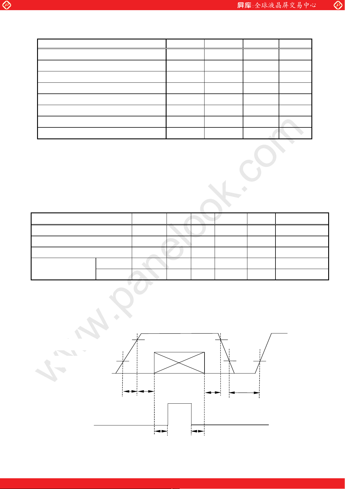
*1) Power and signals sequence:
t1 d10ms 200 ms d t4
0 < t2 d 50 ms 200 ms d t5
0 < t3 d 50 ms 0 d t6
LCD Power Supply
Logic Signal
Backlight Power Supply
0.9VCC
0.1VCC
t1
t2
VCC
data
Backlight
t3
0.9VCC
0.1VCC
t4
0.1VCC
t5 t6
data: RGB DATA, DCLK, DENA, MODE, SC
MITSUBISHIConfidential (5/25) AA121SL08_02_00
One step solution for LCD / PDP / OLED panel application: Datasheet, inventory and accessory!
www.panelook.com
Global LCD Panel Exchange Center
www.panelook.com
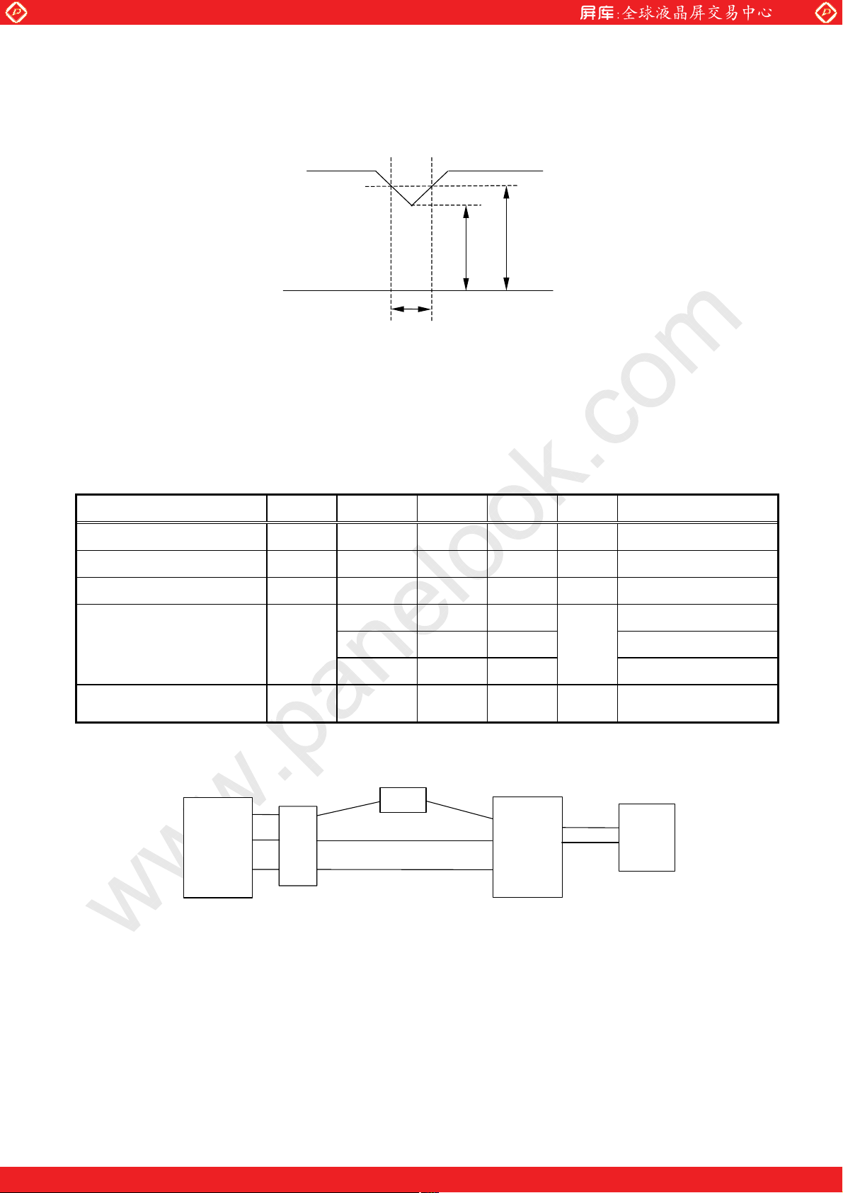
VCC-dip conditions:
1) When 2.6 V
d VCC < 3.0 V, td d 10 ms
2) When VCC < 2.6 V
VCC-dip conditions should also follow the power and signals sequence.
VCC
3.0V
2.6V
td
*2) Typical current condition:
64-gray-bar-pattern (6bit)
256-gray-bar-pattern (8bit)
600 line mode
VCC = +3.3 V , f
=37.9 kHz, fV=60.3 Hz, f
H
= 40 MHz
CLK
(2) Backlight
Ta = 25
ITEM
SYMBOL
MIN. TYP. MAX. UNIT Remarks
Lamp Voltage VL -- 540 -- Vrms IL = 12.0 mArms
Lamp Current IL 6.0 12.0 14.0 mArms
Lamp Frequency FL 30 -- 60 kHz
* 2), *6)
* 3)
1000 -- -- Ta = 25°C
Starting Lamp Voltage VS
1200 -- -- Ta = 0°C
Vrms
1290 -- --
Lamp Life Time LT 50,000 -- -- h
Ta = 20°C
* 4), *5)
IL = 12.0mArms,
Continuous operation
[Note]
*1)Please use synchronous inverter.
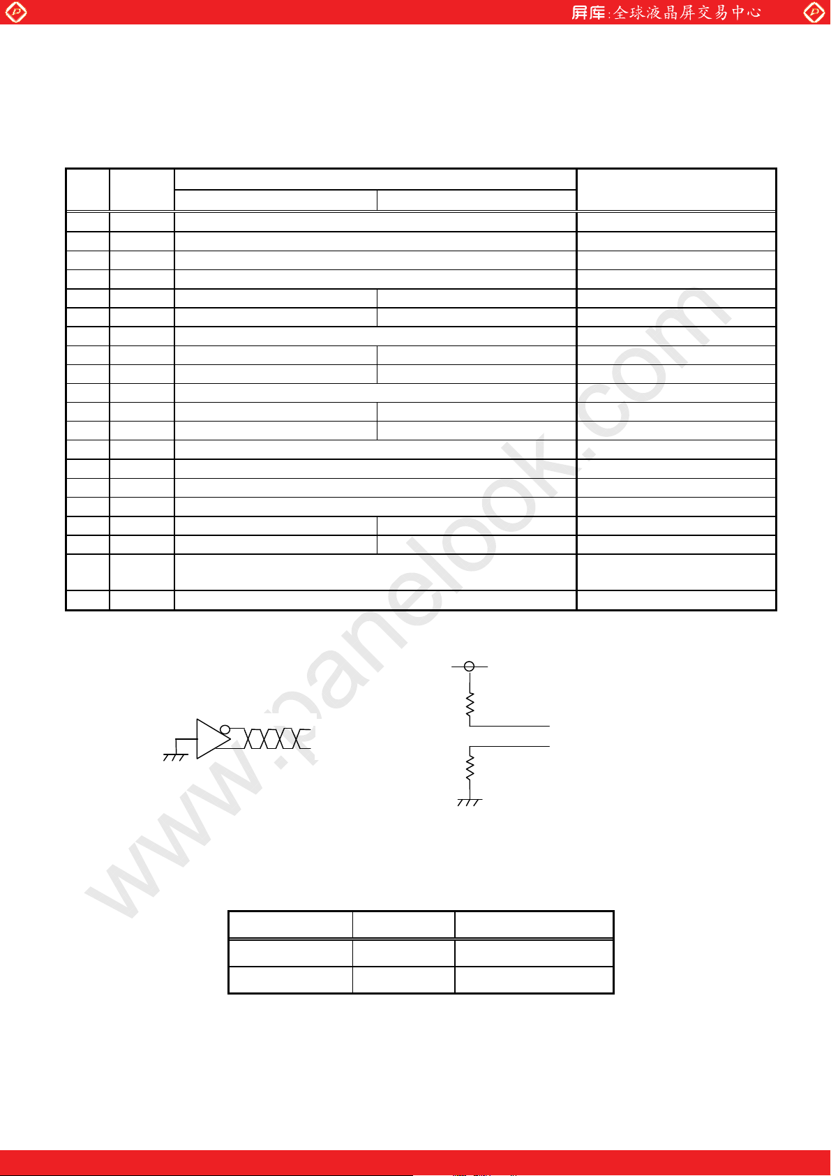
*2) Lamp Current measurement method (The current meter is inserted in low voltage line.)
A
Inverter
Power
Supply
LCD
Module
CTL
CTH
CTH
*3) Lamp frequency of inverter may produce interference with horizontal synchronous frequency,
and this may cause horizontal beat on the display. Therefore, please adjust lamp frequency, and
keep inverter as far from module as possible or use electronic shielding between inverter and
module to avoid the interference.
*4) Lamp life time is defined as the time either when the brightness becomes 50% of the initial
value, or when the starting lamp voltage does not meet the value specified in this table.
*5) The life time of the backlight depends on the ambient temperature. The life time will decrease
under low/high temperature.
MITSUBISHIConfidential (6/25) AA121SL08_02_00
One step solution for LCD / PDP / OLED panel application: Datasheet, inventory and accessory!
www.panelook.com
Global LCD Panel Exchange Center
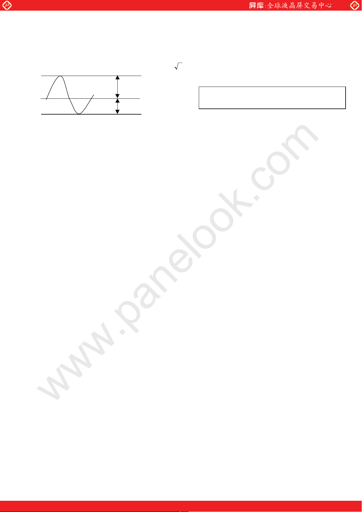
*6) Please use the inverter which has symmetrical current wave form as follows,
The degree of unbalance: less than 10%
www.panelook.com
The ratio of wave height: less than
I
PH
I
PL
IPH: High side peak
: Low side peak
I
PL
±10%
2
The degree of unbalance = |IPH - IPL| / Irms
The ratio of wave height = I
(or IPL) / Irms
PH
100(%)
u
CURRENT WAVE FORM
MITSUBISHIConfidential (7/25) AA121SL08_02_00
One step solution for LCD / PDP / OLED panel application: Datasheet, inventory and accessory!
www.panelook.com
Global LCD Panel Exchange Center
V
5. INTERFACE PIN CONNECTION
(1) CN 1(Interface Signal)
Used connector: FI-SEB20P-HFE (JAE)
Corresponding connector: FI-S20S[for discrete Wire], FI-SE20ME[for FPC] (JAE)
Pin
No.
Symbol
1 VCC
2 VCC
3 GND
4 GND
5 Link 0- R0, R1, R2, R3, R4, R5, G0 R2, R3, R4, R5, R6, R7, G2 R0, R1, R2, R3, R4, R5, G0
6 Link 0+ R0, R1, R2, R3, R4, R5, G0 R2, R3, R4, R5, R6, R7, G2 R0, R1, R2, R3, R4, R5, G0
7 GND
8 Link 1- G1, G2, G3, G4, G5, B0, B1 G3, G4, G5, G6, G7, B2, B3 G1, G2, G3, G4, G5, B0, B1
9 Link 1+ G1, G2, G3, G4, G5, B0, B1 G3, G4, G5, G6, G7, B2, B3 G1, G2, G3, G4, G5, B0, B1
10 GND
11 Link 2- B2, B3, B4, B5, DENA B4, B5, B6, B7, DENA B2, B3, B4, B5, DENA
12 Link 2+ B2, B3, B4, B5, DENA B4, B5, B6, B7, DENA B2, B3, B4, B5, DENA
13 GND
14 CLKIN15 CLKIN+
16 GND
17 Link3- See: *2) R0, R1, G0, G1, B0, B1 R6, R7, G6, G7, B6, B7
18 Link3+ See: *2) R0, R1, G0, G1, B0, B1 R6, R7, G6, G7, B6, B7
19 MODE Low=ISP 6 bit compatibility mode
20 SC
Scan direction control. ( Low : Normal , High : Reverse )
*1) The shielding case is connected with GND.
*2) Recommended wiring of Pin 17,18 (6 bit input)
Function(ISP 6 bit compatibility mode)
6 bit input 8 bit input
+3.3 V Power supply
+3.3 V Power supply
www.panelook.com
GND
GND
GND
GND
GND
Clock -
Clock +
GND
Function(ISP 8 bit
compatibility mode)
m
m
m
m
m
m
m
m
m
m
High=ISP
8 bit compatibility mode
m
LVD S
transmitter
(2) CN 2(Backlight)
Backlight-side connector: BHR-04VS-1 (JST)
Inverter-side connector: SM04(4.0)B-BHS(LF)(SN) (JST)
LOW data
6 8 0
Pin 17
Pin 18
QT
6 2 0
Pin No. Symbol Function
1, 2 CTH VBLH (High voltage)
4 CTL VBLL (Low voltage)
>Note@VBLH - VBLL = VL
CC
ǡ
Pin 17
Pin 18
ǡ
MITSUBISHIConfidential (8/25) AA121SL08_02_00
One step solution for LCD / PDP / OLED panel application: Datasheet, inventory and accessory!
www.panelook.com
 Loading...