

Page 1

type A2USHCPU-S1
User,s Manual
Mitsubishi Programmable Logic Controller
Page 2
SAFETY PRECAUTIONS
(Read these precautions before usi ng.)
When using Mitsubishi equipment, thoroughly read this manual and the associated manuals
introduced in the manual. Also pay careful attention to safety and handle the module properly.
These
and “CAUTION”.
Depending on circumstances, procedures indicated by
results.
In any case, it is important to follow the directions for usage.
Store this manual in a safe place so that you can take it out and read it whenever necessary. Always
forward it to the end user.
SAFETY PRECAUTIONS classify the safety precautions into two categories: “DANGER”
DANGER
CAUTION
Procedures which may lead to a dangerous condition and cause death or
serious injury if not carried out properly.
Procedures which may lead to a danger ous condition a nd caus e super ficial
to medium injury, or physical da mage only, if not carried out properly.
CAUTION
may also be linked to serious
[DESIGN PRECA UTION S]
!
DANGER
•
Install a safety circuit external to the PC that keeps the entire system safe even when there are
problems with the external power supply or the PC main module. Otherwise, trouble could result
from erroneous output or malfunction.
(1) Configure the following circuits outside the PC: emergency stop circuit, protection circuit,
interlocking circuit for opposite operations such as forward and reverse operations, and
interlocking circuit for machine damage prevention such as upper/lower limit for positioning.
(2) When the PC detects the following problems, it will stop calculation and turn off all output.
•
The power supply module has an over current protection device and over voltage
protection device.
•
The PC CPUs self-diagnostic functions, such as the watchdog timer error, detect problems.
In addition, all output will be turned on when there are problems that the PC CPU cannot
detect, such as in the I/O controller. Build a failsafe circuit exterior to the PC that will make
sure the equipment operates safely at such times.
Refer to the Section 8.1 in this manual for example failsafe circuits.
(3) Output could be left on or off when there is trouble in the output module’s relay or transistor.
So, build an external monitoring circuit that will monitor any single output that could cause
serious trouble.
•
If current over the rating or over-current due to a load short-circuit flows for a long term, it may
cause smoke or fire. Prepare an external safety circuit, such as a fuse.
•
Build a circuit that turns on the external power supply when the PC main module power supply is turned
on. If the external power supply is turned on first, it could result in erroneous output or malfunction.
Page 3
[DESIGN PRECA UTION S]
!
DANGER
Build a circuit that turns on the external power supply after the PLC main module power is turned
•
on.
If the external power supply is turned on first, it could result in accidents due to erroneous
outputs or a malfunction.
When there are communication faulty with the data link, the communication faulty stat ion will
•
enter the following condition. Build an interlock circuit into t he PLC program t hat w ill make sure
the system operates safely by using the communication state information.
Not doing so could result in erroneous output or malfunction.
(1) For the data link data, the data prior t o the communicat ion error will be held.
(2) The MELSECNET (II, /B, /10) remote I/O station will turn all output off.
(3) The MELSECNET/MINI-S3 remote I/O station will hold the output or turn all output off
depending on the E.C. mode setting.
Refer to manuals for corresponding data link system for how to detect the communication faulty
station and the operation status when a communication error occurred.
When configuring a system, do not leave any slots vacant on the base. Should there be any
•
vacant slots, always use a blank cover (A1SG60) or dummy module (A1SG62).
If the cover is not attached, the module's internal parts may be dispersed w hen a short-circuit
test is performed or overcurrent/overvoltage is accidentally applied to the external I/O area.
!
CAUTION
Do not bunch the control wires or communication cable with the main circuit or power wires, or
•
install them close to each other.
They should be installed 100mm (3.94 inch) or more from each other.
Not doing so could result in noise that would cause malfunction.
When controlling items like lamp load, heater or solenoid valve using an out put module, large
•
current (approximately ten times greater than that present in normal circumstances) may flow
when the output is turned OFF
having sufficient rated current.
ON. Take measures such as replacing the module with one
[INSTALLATION PRECAUTIONS]
!
CAUTION
Use the PLC in the environment given in the general specification section of the manual.
•
Using the PLC outside the range of the general specifications may result in electric shock, fire,
or malfunction or may damage or degrade the product.
Before mounting the module, securely insert the projection at the bottom of the module into the
•
fixing hole on the base module.
(The AnS series module must be tightened to the base module at the specified tightening torque.)
An improperly mounted module may result in malfunct ion, failur e, or falling.
Excessive screw tightening may cause falling due to the breakage of the screw or module,
short-circuit, or malfunction.
Page 4
[INSTALLATION PRECAUTIONS]
!
CAUTION
Tighten the screw within the range of specified torque.
•
If the screws are loose, it may result in fallout, short circuits, or malfunctions.
Tightening the screws too far may cause damage to the screw and/or the module, resulting in
fallout, short circuits, or malfunction.
When installing extension cables, be sure that the base unit and the module connectors are
•
installed correctly. After installation, check them for looseness. Poor connections could result in
erroneous input and erroneous output.
Correctly connect the memory card installation connector to the memory card. After installation,
•
make sure that the connection is not loose. A poor connection could result in malfunction.
Do not directly touch the module’s conductive parts or electronic components.
•
Doing so could cause malfunction or failure in the module.
[WIRING PRECAUTIONS]
!
DANGER
Completely turn off the external pow er supply when inst alling or w iring. Not completely tu rning
•
off all power supply could result in electric shock or damage to the product.
When turning on the power or operating the module after installation or wiring work, be sure that
•
the module’s terminal covers are correctly attached. Not attaching t he terminal covers could
result in electric shock.
!
CAUTION
Be sure to ground the FG terminals and LG terminals with a special PLC ground of Type 3 or
•
above. Not doing so could result in electric shock or malfunction.
When wiring in the PLC, check the rated voltage and terminal layout of the wiring, and make
•
sure the wiring is done correctly. Connecting a power supply that differs from the rated voltage
or wiring it incorrectly may cause fire or breakdown.
Do not connect multiple power supply modules in parallel.
•
Doing so could cause overheating, fire, or damage to the power supply module.
Tighten the terminal screws with the specified torque.
•
If the terminal screws are loose, it could result in short circuits, fire, or malfunction.
Tightening the screws too far may cause damage to the screw and/or the module, resulting in
fallout, short circuits, or malfunction.
Take care so that foreign matter such as chips and wiring scraps do not enter the module as it
•
could result in fire, trouble or a malfunction.
External connections shall be crimped or pressure welded with the specified tools, or correctly
•
soldered.
For information regarding the crimping and pressure welding tools, refer to the I/O module’s user
manual. Imperfect connections could result in short circuit, fires, or malfunction.
Page 5
[STARTING A ND MAINTENANCE PRECAUTIONS]
!
DANGER
Do not touch the terminals while power is on. Doing so could cause shock or malfunction.
•
Correctly connect the battery. Also, do not change, disassemble, heat , place in fire, short circuit,
•
or solder the battery.
Mishandling of the battery can cause overheating or cracks which could result in injury and fires.
Make sure to switch all phases of the external power supply off before cleaning or re-tightening
•
screws. If you do not switch off the ext ernal pow er supply , it will cause electr ic shock.
If the screws are loose, it may result in fallout, short circuit, or malfunction. Tightening the
screws too far may cause damages to the screws and/or the module, resulting in fallout, short
circuits, or malfunction.
!
CAUTION
Carefully read manuals and confirm that it is safe enough before performing on-line operations
•
which require to connect peripheral devices to an operating CPU module. (especially w hen
modifying a program, performing forced output, or modifying the operation status.)
Misoperation may damage the module or cause accidents.
Do not disassemble or rebuild the module.
•
It may cause accidents, malfunction, injury, or fire.
When using a cellular phone, keep it 25 cm or more away from the PLC.
•
Otherwise, malfunction may result.
Make sure to switch all phases of the external power supply off before mounting or removing the
•
module. If you do not switch off the exter nal power supply, it w ill cause failure or malfunction of
the module.
[DISPOSAL PRECAUTIONS]
!
Disposing of this product, treat it as industrial wast e.
•
CAUTION
Page 6

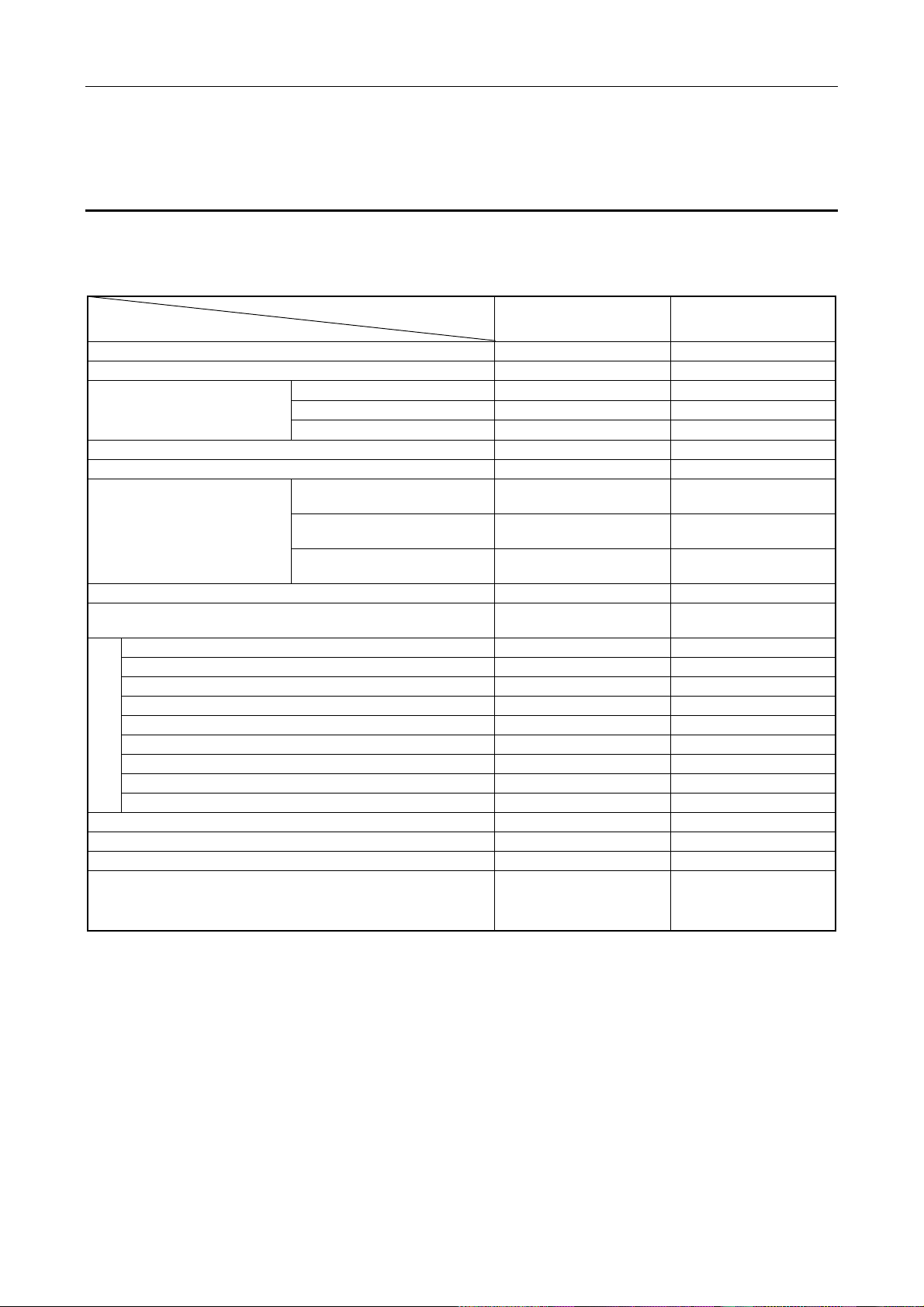
Revisions
* The manual number is noted at the lower left of the back cover.
Print Date *Manual Number Revision
Jun. 1997 IB(NA)-66789-A First printing
Jun. 2002
IB(NA)-66789-B
Equivalent to the Japanese version C
Correction
SAFETY PRECAUTIONS, Chapter 1, Section 1.2, Section 2.1, 2.2.1, 2.2.2,
2.2.3, 2.3, Chapter 3, Section 4.1.4, 4.2.2, 4.2.5, Section 5.1, 5.2, Section
6.1.2, 6.1.3, Section 7.1.1, 7.1.5, Section 8.1, Chapter 9, Section 10.3.2,
Appendix 2.1, 2.2, Appendix 4.2
This manual does not imply guarantee or implementation right for industrial ownership or implementation
of other rights. Mitsubishi Electric Corporation is not responsible for industrial ownership problems caused
by use of the contents of this manual.
1997 Mitsubishi Electric Corporation
Page 7

Introduction
Thank you for choosing a Mitsubishi MELSEC-A Series General Purpose Programmable Controller.
Before using your new PC, please read this manual thoroughly to gain an understanding of its functions so
you can use it properly.
Please forward a copy of this manual to the end user.
Table of Contents
About This Manual
1. OVERVIEW 1- 1 to 1- 3
1.1 Features............................................................................................................................................................ 1- 2
1.2 Comparison of Performance and Specifications with A2USCPU(S1)...............................................................1- 3
2. SYSTEM CONFIGURATION 2- 1 to 2- 19
2.1 Overall Configuration ........................................................................................................................................ 2- 1
2.2 Precautions When Configuration the System ................................................................................................... 2- 3
2.2.1 Hardware ............................................................................................................................................... 2- 3
2.2.2 Software package.................................................................................................................................. 2- 5
2.2.3 Precautions when using GPP function software packages and A8PU peripheral devices
which are not compatible with AnU........................................................................................................ 2- 7
2.3 System Equipment............................................................................................................................................ 2- 8
2.4 System Configuration Overview........................................................................................................................2-18
3. GENERAL SPECIFICATION 3- 1
4. CPU MODULE 4-1 to 4- 28
4.1 Performance Specification................................................................................................................................ 4- 1
4.1.1 Overview of operation processing..........................................................................................................4- 3
4.1.2 Operation processing of RUN, STOP, PAUSE, and STEP RUN...........................................................4- 5
4.1.3 Operation processing upon momentary power failure........................................................................... 4- 7
4.1.4 Self-diagnosis........................................................................................................................................4- 8
4.1.5 Device list ..............................................................................................................................................4-10
4.2 Parameter Setting Ranges................................................................................................................................4-11
4.2.1 List of parameter setting range..............................................................................................................4-11
4.2.2 Memory capacity setting (for main program, file register, comment, etc.).............................................4-13
4.2.3 Setting ranges of timer and counter.......................................................................................................4-15
4.2.4 I/O devices.............................................................................................................................................4-17
4.2.5 I/O allocation of special function modules .............................................................................................4-17
4.2.6 MELSECNET/MINI-S3 automatic refresh..............................................................................................4-18
4.3 Function List......................................................................................................................................................4-22
4.4 Precautions When Handling the Module...........................................................................................................4-24
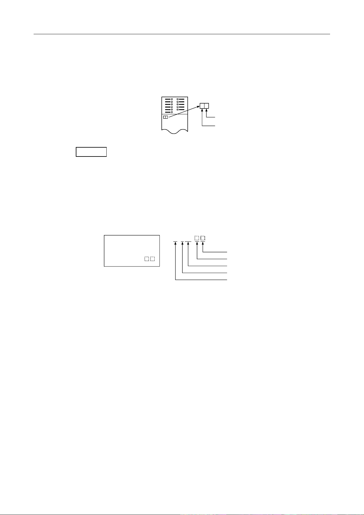
4.5 Name and Setting of Each Part.........................................................................................................................4-25
4.5.1 The name of each part of the A2USHCPU-S1.......................................................................................4-25
4.5.2 Settings for memory protection switch...................................................................................................4-27
4.5.3 Latch clear operation.............................................................................................................................4-28
5. POWER SUPPLY MODULE 5- 1 to 5- 7
5.1 Specifications.................................................................................................................................................... 5- 1
5.1.1 Selecting a power supply module.......................................................................................................... 5- 4
Page 8

5.2 Name and Setting of Each Part......................................................................................................................... 5- 5
6. BASE UNIT AND EXTENSION CABLE 6- 1 to 6- 7
6.1 Specification...................................................................................................................................................... 6- 1
6.1.1 Base unit specifications.........................................................................................................................6- 1
6.1.2 Extension cable specifications............................................................................................................... 6- 1
6.1.3 Usage standards of extension base units
(A1S52B, A1S55B, A1S58B, A52B, A55B, A58B)...............................................................................6- 2
6.2 Name and Setting of Each Part......................................................................................................................... 6- 6
7. MEMORY CASSETTE AND BATTERY 7- 1 to 7- 5
7.1 Memory Cassette.............................................................................................................................................. 7- 1
7.1.1 Specifications......................................................................................................................................... 7- 1
7.1.2 Precautions when handling the memory cassette.................................................................................7- 1
7.1.3 Installation and removal of memory cassette ........................................................................................ 7- 2
7.1.4 Procedure for writing sequence program to A2SMCA-14KP.................................................................7- 3
7.1.5 Memory protection setting of A2SNMCA-30KE.....................................................................................7- 4
7.2 Battery............................................................................................................................................................... 7- 5
7.2.1 Specifications......................................................................................................................................... 7- 5
7.2.2 Precautions when handling.................................................................................................................... 7- 5
7.2.3 Battery installation ................................................................................................................................. 7- 5
8. LOADING AND INSTALLATION 8- 1 to 8- 17
8.1 Concept of Failsafe Circuit................................................................................................................................ 8- 1
8.2 Installation Environment.................................................................................................................................... 8- 5
8.3 Calculation Method of Heat Amount Generated by the PC............................................................................... 8- 5
8.4 Installation of Base Unit.................................................................................................................................... 8- 7
8.4.1 Precautions when installing PC.............................................................................................................8- 7
8.4.2 Installation.............................................................................................................................................. 8- 8
8.5 Installation and Removal of the Modules.......................................................................................................... 8- 9
8.6 Installation and Removal of the Dustproof Cover..............................................................................................8-12
8.7 Wiring................................................................................................................................................................8-13
8.7.1 Precautions when wiring........................................................................................................................8-13
8.7.2 Wiring to the module terminals..............................................................................................................8-16
8.8 Precautions When Unfailure Power System (UPS) is Connected ....................................................................8-17
9. EMC DIRECTIVE AND LOW-VOLTAGE INSTRUCTION 9- 1 to 9- 11
9.1 Requirements for Compliance to EMC Directive (89/336/EEC)........................................................................ 9- 1
9.1.1 EMC standards...................................................................................................................................... 9- 1
9.1.2 Installation inside the control cabinet..................................................................................................... 9- 2
9.1.3 Cables.................................................................................................................................................... 9- 3
9.1.4 Power supply module............................................................................................................................. 9- 6
9.1.5 Ferrite core ............................................................................................................................................ 9- 7
9.1.6 Noise filter (power supply line filter)....................................................................................................... 9- 7
9.2 Requirement to Conform to the Low-Voltage Instruction.................................................................................. 9- 8
9.2.1 Standard applied for AnS series............................................................................................................ 9- 8
9.2.2 Precautions when using the AnS series................................................................................................9- 9
9.2.3 Power supply ......................................................................................................................................... 9- 9
9.2.4 Control box.............................................................................................................................................9-10
9.2.5 Module installation.................................................................................................................................9-10
9.2.6 Grounding..............................................................................................................................................9-11
9.2.7 External wiring .......................................................................................................................................9-11
Page 9

10. MAINTENANCE AND INSPECTION 10- 1 to 10- 5
10.1 Routine Inspection............................................................................................................................................10-2
10.2 Periodic Inspection............................................................................................................................................10-3
10.3 Battery Replacement.........................................................................................................................................10-4
10.3.1 Service life of the battery .......................................................................................................................10-4
10.3.2 Battery replacement procedure .............................................................................................................10-5
11. TROUBLESHOOTING 11- 1 to 11- 20
11.1 Fundamentals of Troubleshooting ....................................................................................................................11- 1
11.2 Troubleshooting................................................................................................................................................11- 2
11.2.1 Troubleshooting flowchart......................................................................................................................11- 2
11.2.2 Flowchart for actions when the "POWER" LED is turned OFF..............................................................11- 3
11.2.3 Flowchart for actions when the "RUN" LED is turned OFF....................................................................11- 4
11.2.4 Flowchart for actions when the "RUN" LED is flashing..........................................................................11- 5
11.2.5 Flowchart for actions when the "ERROR" LED is turned ON.................................................................11- 6
11.2.6 Flowchart for actions when the "ERROR" LED is flashing.....................................................................11- 7
11.2.7 Flowchart for actions when the output module's output load does not turn ON.....................................11- 8
11.2.8 Flowchart for actions when the program cannot be written ...................................................................11- 9
11.3 Error Code List..................................................................................................................................................11-10
11.3.1 Procedure to read an error code............................................................................................................11-10
11.3.2 Error code list.........................................................................................................................................11-10
11.4 Possible Troubles with I/O Modules..................................................................................................................11-18
11.4.1 Troubles with the input circuit and the countermeasures ......................................................................11-18
11.4.2 Possible troubles in the output circuit ....................................................................................................11-20
APPENDIX A- 1 to A- 31
Appendix 1 Instruction List....................................................................................................................................... A- 1
Appendix 2 Lists of Special Relays and Special Registers...................................................................................... A- 8
Appendix 2.1 List of special relays.................................................................................................................A- 8
Appendix 2.2 List of special registers.............................................................................................................A-13
Appendix 3 Peripheral Devices................................................................................................................................A-19
Appendix 4 Precautions When the Existing Sequence Programs Are Diverted for the A2USHCPU-S1.................A-20
Appendix 4.1 Instructions with different specifications...................................................................................A-20
Appendix 4.2 Special relays and special registers with different specifications.............................................A-21
Appendix 4.3 Parameter setting.....................................................................................................................A-21
Appendix 4.4 I/O control method....................................................................................................................A-22
Appendix 4.5 Microcomputer program ...........................................................................................................A-23
Appendix 4.6 Processing of the index register...............................................................................................A-23
Appendix 5 External Dimension Diagrams...............................................................................................................A-24
Appendix 5.1 A2USHCPU-S1 module ...........................................................................................................A-24
Appendix 5.2 A1S61PN, A1S62PN and A1S63P power supply modules......................................................A-24
Appendix 5.3 Basic Base Unit........................................................................................................................A-25
Appendix 5.3.1 A1S32B basic base unit................................................................................................A-25
Appendix 5.3.2 A1S33B basic base unit................................................................................................A-25
Appendix 5.3.3 A1S35B basic base unit................................................................................................A-26
Appendix 5.3.4 A1S38B basic base unit................................................................................................A-26
Appendix 5.4 Extension Base unit..................................................................................................................A-27
Appendix 5.4.1 A1S65B extension base unit.........................................................................................A-27
Appendix 5.4.2 A1S68B extension base unit.........................................................................................A-27
Appendix 5.4.3 A1S52B extension base unit.........................................................................................A-28
Appendix 5.4.4 A1S55B extension base unit.........................................................................................A-28
Appendix 5.4.5 A1S58B extension base unit.........................................................................................A-29
Appendix 5.5 Memory Cassette .....................................................................................................................A-29
Page 10

Appendix 5.5.1 A2SMCA- memory cassette.....................................................................................A-29
Appendix 5.5.2 A2SNMCA-30KE memory cassette...............................................................................A-30
Appendix 5.6 A2SWA-28P Memory Write Adapter........................................................................................A-30
Appendix 6 Precautions When Writing Data on a ROM Using PECKER..................................................................A-31
Page 11

About This Manual
The following table lists manuals regarding this product.
Related Manuals
Manual Name
ACPU Programming Manual (Fundamentals)
Describes programming methods necessary for creating programs, device names, parameters,
program types, memory area configuration, and so on.
(Sold separately)
ACPU Programming Manual (Common Instructions)
Describes how to use the sequence instruction, basic instructions, applied instructions and
microcomputer programs.
(Sold separately)
AnACPU/AnUCPU/QCPU-A (A mode) Programming Manual (Dedicated Instructions)
Describes instructions that have been expanded for A2USHCPU-S1.
(Sold separately)
AnACPU/AnUCPU Programming Manual (AD57 Instructions)
Describes dedicated instructions for A2USHCPU-S1 to control the AD57(S1)/AD58 controller
module.
(Sold separately)
AnACPU/AnUCPU Programming Manual (PID Instructions)
Describes dedicated instructions for A2USHCPU-S1 to perform the PID control.
(Sold separately)
AnS Module type I/O User's Manual
Describes the specification of the compact building block type I/O module.
(Sold separately)
Manual No.
(Model Code)
IB-66249
(13J740)
IB-66250
(13J741)
IB-66251
(13J742)
IB-66257
(13J743)
IB-66258
(13J744)
IB-66541
(13JE81)
Page 12

1. OVERVIEW MELSEC-A
1. OVERVIEW
This User's Manual describes the performance, functions, and handling method of the A2USHCPU-S1
general purpose PC (abbreviated as A2USHCPU-S1 hereafter), as well as the specifications and
handling of the memory cassette, power supply module and the base module.
The A2USHCPU-S1 has higher performance compared with the conventional A2USCPU, with faster
instruction processing speed, increased program size, and so on. Utilize these enhanced capabilities to
operate the A2USHCPU-S1 in the most efficient way.
The instructions used in the sequence programs of the A2USHCPU-S1 are as follows:
•
Sequence instructions........................25 instructions
•
Basic and application instructions ......243 instructions
•
Dedicated instructions........................204 instructions
Refer to Appendix-1 for the complete list of instructions.
The programming modules and software packages have to be compatible with the upgraded A2UCPU,
A2UCPU-S1, A3UCPU, and A4UCPU (abbreviated as AnUCPU hereafter).
When the conventional programming modules and software packages are used, the usable range
varies depending on the model of the CPU (PC model name). --- Refer to Section 2.2.3.
Refer to the list of components in Section 2.3 for various modules which can be used with the
A2USHCPU-S1.
Refer to Section 2.2.1 for the special function modules which have limited range of usable devices.
1-1
Page 13

1. OVERVIEW MELSEC-A
1.1 Features
The A2USHCPU-S1 has the following features when compared with A2USCPU(S1) and A1SCPU:
(1) The program size was greatly increased in the A2USHCPU-S1 to a maximum of 30k steps,
compared with 14k steps of the A2USCPU(S1).
(2) The operation speed (sequence instructions) was substantially improved.
The processing speed of the A2USHCPU-S1 has been improved to 0.09µs/step, compared with
0.2µs/step for the A2USCPU.
(3) The A2USHCPU-S1 has 256k bytes of built-in RAM memory.
The built-in RAM memory has a capacity of 256k bytes with battery backup.
In addition, an optional memory cassette (EPROM, EEPROM) can be attached.
(4) MELSECNET/10-compatible for fast and large-capacity networking
The MELSECNET/10 network system can be constructed by installing a network module
(A1SJ71LP21, A1SJ71BR11) to the extension base module and setting the network parameters.
It is also compatible with the MELSECNET II system.
(5) The A2USHCPU-S1 has more points for the I/O devices, link devices, and data registers than
those of the A1SCPU.
•
I/O device (X/Y)......8192 points (X/Y0 to 1FFF)
•
Link relay (B) ..........8192 points (B0 to B1FFF)
•
Link register (W).....8192 points (W0 to W1FFF)
•
Data register (D)..... 8192 points (D0 to 8191)
(6) The A2USHCPU-S1 can execute the batch processing of the data communication requests.
•
All of the data communication requests from the A1SJ71UC24-R2, A1SD51S, peripheral
devices, and others, can be processed by single END processing. (Normally, one END
processing processes one communication request.)
•
The batch processing of the data communication requests can be activated by selecting "YES"
on the "END Batch Processing Setup" in the supplementary function setup of the parameter, or
by turning ON the M9029 from the sequence program.
•
Delay of the data transfer to each module will be prevented by using the batch processing of
the data communication requests.
(M9029: When OFF, only one request is processed by one scan.)
(7) The A2USHCPU-S1 can execute the dedicated instructions for the AnA/AnUCPU.
Dedicated instructions for AnA/AnUCPU, AD57 instructions, and PID control instructions can be
executed.
1-2
Page 14
1. OVERVIEW MELSEC-A
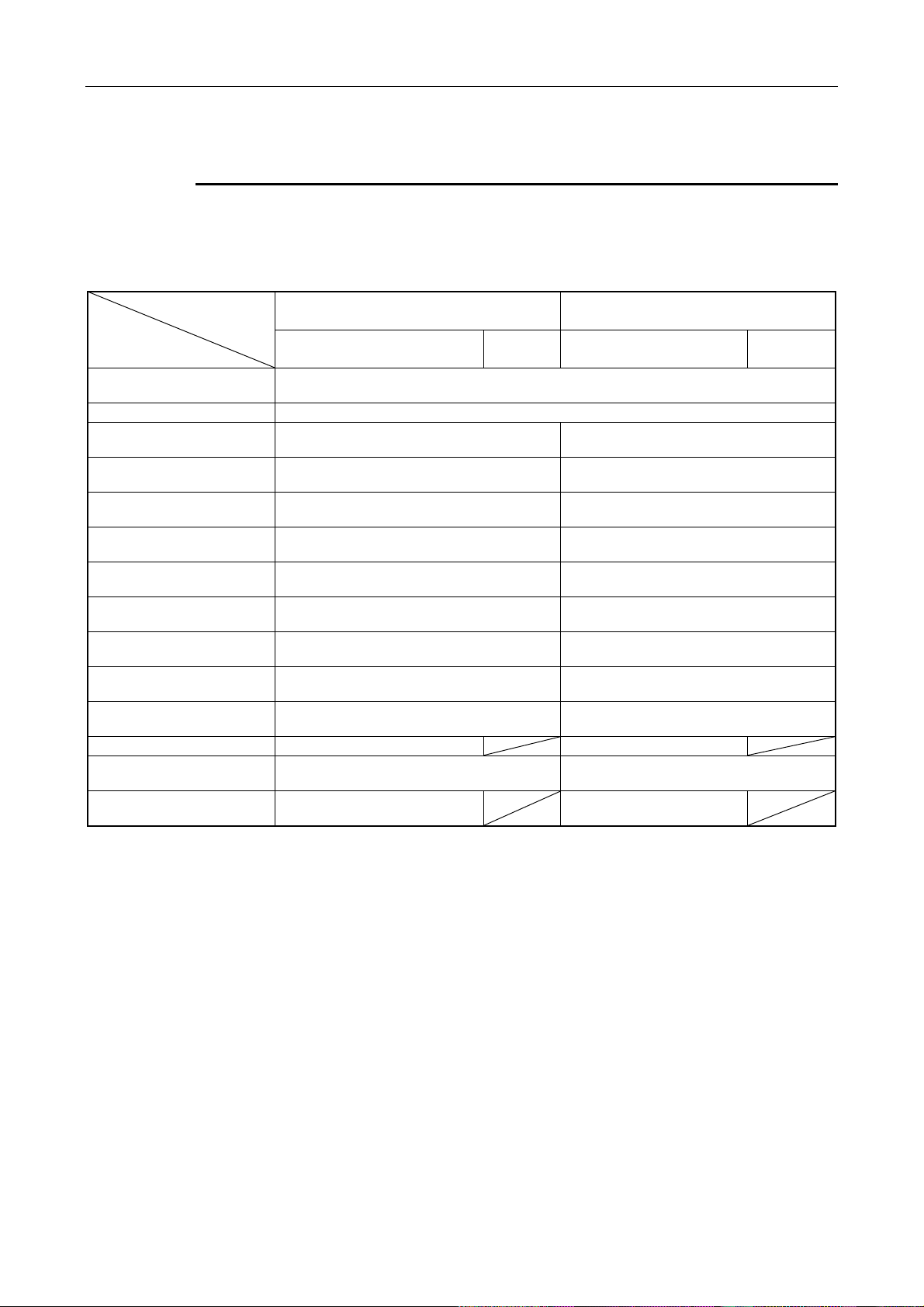
1.2 Comparison of Performance and Specifications with
A2USCPU(S1)
The differences in performance and specifications between A2USHCPU-S1 and A2USCPU(S1) are as
follows. Performance and specifications which are not listed here are the same between A2USHCPUS1 and A2USCPU(S1).
CPU Model
Item
I/O Control method Refresh method Refresh method
Processing speed (Sequence instruction) (µs/step) 0.09 0.2
Sequence instructions
Number of instructions
Constant scan (ms) 10 to 190 10 to 190
Main program capacity A maximum of 30k steps A maximum of 14k steps
Memory capacity and memory
cassette model
Number of I/O device points (points ) 8192 8192
Number of I/O points (points) 1024
Internal relay [M, L, S] (points) 8192 8192
Link relay [B] (points) 8192 8192
Link register [W] (point s ) 8192 8192
Data register [D] (points) 8192 8192
File register [R] (points 8192 8192
Annunciator [F] (points) 2048 2048
Timer [T] (points) 2048 2048
Counter [C] (points) 1024 1024
Number of device points
Index register [V, Z] (points) 14 14
Comment (points) MAX 4032 MAX 4032
Expanded comment (points) MAX 3968 MAX 3968
Watchdog timer set t ing Fixed to 200(ms) Fixed to 200(ms)
Data link
Basic and application instructions 243 243
Dedicated instructions 204 204
Memory capacity
(built-in RAM)
EPROM-type
memory cassette
2
E
PROM-type
memory cassette
*1 When A2USCPU-S1 is used.
A2USHCPU-S1 A2USCPU(S1)
25 25
256k bytes
A2SMCA-14KP A2SMCA-14KP
A2SNMCA-30KE A2SNMCA-30KE
MELSECNET/10 MELSECNET/10
MELSECNET(II) MELSECNET(II)
MELSECNET/B MELSECNET/B
64k bytes
(256k bytes)*1
512
(1024)*1
1-3
Page 15
2. SYSTEM CONFIGURATION MELSEC-A
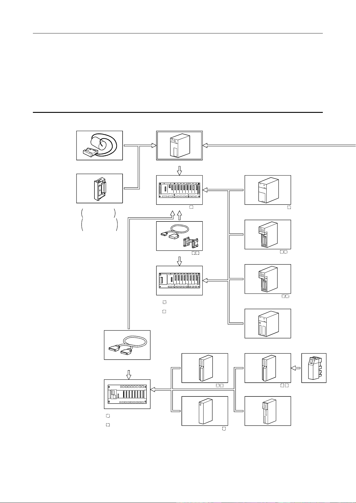
2. SYSTEM CONFIGURATION
The possible system configuration with A2USHCPU-S1, the precautions when the system is
configured, and system components are described.
2.1 Overall Configuration
The system configurations of the A2USHCPU-S1 stand-alone system and the peripheral devices are
as follows:
(To peripheral devices)
Battery (A6BAT)
ROM casette
A2SMCA-14KP
with EPROM
A2SMCA-14KE
A2SNMCA-30KE
2
PROM
with E
A2USHCPU-S1
Basic base (A1S3 B)
Extension cable (A1SC B)
Extension base
(A1S5 B)
: without power supply module
(A1S6 B)
: with a power supply module
Power supply module (A1S6 P)
Input module (A1SX )
Output module (A1SY )
Connection cable (A1SCO5NB)
[For building-block type]
Extension base
(A5 B)
: without power supply module
(A6 B)
: with a power supply module
Input module (AX )
Power supply module (A6 P)
2-1
Special function module
Output module (AY )
Special function module
Fuse
Page 16
2. SYSTEM CONFIGURATION MELSEC-A
(To A2USHCPU-S1 )
AC30R4
AC300R4
cable
AC30R4-PUS
cable
AC20R4-A8PU
cable
A6PHP
Plasma Hand-held
Graphic Programmer
A6GPP
Intelligent GPP
A7PUS
programming module
A8PU/A8UPU
programming module
AC03R2
cable
AC30R2
cable
EPROM write adapter
(A2SWA-28P)
A6WU
P-ROM writer
module
Printer
(A7NPR-S1, K6PR-K,
general-purpose printer)
ROM cassette
(A2SMCA-14KP)
EPROM write
adapter
(A2SWA-28P)
ROM cassette
(A2SMCA-14KP)
RS-232C
RS-422 converter
AC30R4-PUS
cable
IBM PC/AT or
100% compatible
A6DU-B
data access module
(When a DOS/V personal computer is used, refer to
the system configuration section of the SW IVD-GPPA,
GX Developer Operation Manual.)
2-2
Page 17
2. SYSTEM CONFIGURATION MELSEC-A
2.2 Precautions When Configuring the System
The hardware and software packages which can be used for the A2USHCPU-S1 are described.
2.2.1 Hardware
(1) I/O module
All the building-block-type I/O modules for A
extension base module of A5
B/A6 B.
(2) Special function module
(a) Special function modules for A N and A A can be used by installing them in the
extension base module of A5
B/A6 B.
(b) The special function modules of the following models have a limitation in the number of
installable modules.
AJ71C22-S1 AD51H-S3 *2
AJ71C23-S3 AJ71UC24
AJ71E71-S3 *2
AJ61BT11 (Only when in the intelligent mode.)
A985GOT (Only when the bus connection is used.)
A975GOT (Only when the bus connection is used.)
A970GOT (Only when the bus connection is used.)
A960GOT (Only when the bus connection is used.)
A956WGOT (Only when the bus connection is used.)
A956GOT (Only when the bus connection is used.)
A951GOT
A1SJ71UC24-R2(PRF/R4)
A1SJ71E71-B2-S3(-B5-S3)
A1SD51S A1SD21-S1
A1SJ61BT11(Only when in the intelligent mode.)
AI61(S1)
A1SI61
AJ71AP21 (S3) *2 AJ71AR21 *2
AJ71AT21B *2
A1SJ71AP21 (S3) *2 A1SJ71AR21 *2
A1SJ71AT21B *2
AJ71LP21 AJ71BR11
AJ71LR21 A1SJ71BR11
A1SJ71LP21
A1SJ71LR21
AJ71PT32-S3 (Only when in the extension mode.)
AJ71T32-S3 (Only when in the extension mode.)
A1SJ71PT32-S3 (Only when in the extension mode.)
A1SJ71T32-S3 (Only when in the extension mode.)
*1: Accessible within the device range of A3HCPU.
*2: Accessible within the device range of A3ACPU.
Refer to the user's manual of the corresponding special f unction module for the acc essible device
ranges.
N and A A can be used by installing them to the
A maximum of 6 modules in total can be installed.
Only one module can be installed.
A maximum of 2 modules
in total can be installed.
A maximum of 4 modules
in total can be installed.
A maximum of 4 modules
in total can be installed.
A maximum of 10 modules in total can be installed.
2-3
Page 18
2. SYSTEM CONFIGURATION MELSEC-A
)
(c) When a remote I/O network is constructed with the MELSECNET/10 network system,
use the A2USHCPU-S1 software of version "A" or later, and the AJ7ILP21/BR11,
A1SJ71LP21/BR11-type network software of version "J" or later.
<Example> For AJ71LP21/BR11:
Software version
Hardware version
Front side of the module
REMARK
The special function modules which cannot be used by the A2USHCPU-S1 are as follows:
AJ71C23
•
AJ71C24 (modules dated before February 1987) • AD51 (modules dated before March 1987)
•
AD57-S2
•
Confirm the manufactured date on the rating plate.
(3) Peripheral devices
(a) Use an A6WU P-ROM writer of the hardware version "E" or later.
<Example> If manufactured date is March 1987:
A6WU
DATE H 703
H 703
Software version
Hardware version
Month
Year (The last digit of the year.
Indicates A3HCPU-compatible.
(b) The A6WU P-ROM writer module cannot be installed as an add-on to be directly attached to
the A2USHCPU-S1.
(c) Among the programming modules (A7PUS, A8PU, A8UPU), only A7PUS is installed as an
add-on.
Other models (A8PU, A8UPU) use only the hand-held method with a cable.
(4) Writing on the ROM for EPROM memory cassettes
An optional A2SWA-28P memory write adapter is required to write on a ROM for the A2SMCA14KP EPROM memory cassette using the A6GPP, A6WU, or ROM writer. (The conventional
A6WA-28P cannot be used.)
(5) Writing while running when operated by E
When "write while running " to the E
2
PROM is executed, the program transfer in progress status is
2
PROM (with A2SNMCA-30KE installed)
displayed on the peripheral device, then the processing for the sequence program is stopped for
approximately two seconds until the transfer finishes to complete the "write while running ".
Because the program processing stops for two seconds, stop the CPU while writing instead of
executing the "write while running " if it affects the operation of the controlled device.
When "A3A" or "A3H" is specified as the PC's model to startup the GPP function software
package which is not AnU-compatible, the "write while running" cannot be executed to the
2
E
PROM.
If "write while running" to the E2PROM is executed, the changed circuit block and any PLF
instruction included in the steps after the instruction will not operate normally.
If the execution condition for the PLF instruction is turned off upon completion of writing, the PLF
instruction is executed.
2-4
Page 19
2. SYSTEM CONFIGURATION MELSEC-A
(6) Writing while in operation by the E2PROM (with A2SNMCA-30KE installed)
(a) When writing a program to the E
2
PROM after the GPP function software package is started
up with the PC's model specified as "A3A" or "A3H", cancel the memory protection of both
the A2USHCPU-S1 main module and the memory cassette for the E2PROM (A2SNMCA30KE) before execution.
(b) The writing of the program cannot be executed from the computer link module or from a
peripheral device connected to other stations on the MELSECNET.
Perform writing of the program from a peripheral device connected to the RS-422 of the
A2USHCPU-S1.
2.2.2 Software package
(1) GPP function software packages and model name setting at the startup
The table below shows the GPP function software packages allowing you to create an
A2USHCPU-S1 program and PLC model settings at startup.
When creating an A2USHCPU-S1 program, if "A2USH-S1" is not available as a PLC model, set
"A3U". If "A3U" is not available, set "A3A". If both "A3U" and "A3A" are not available, set "A3H" .
Peripheral
Device
A6PHP
A6GPP
IBM PC/AT
NOTE
1. As the PC's model for the GPP function software package (SW IVD-GPPA; is older than
3) is set to "A3U", attention should be paid to the following:
1) When a LED or LEDC instruction is written, it is not usable but no error will be issued.
2) When a CHG instruction is written, it is not usable, and the error code 13 and detailed error
code 134 will be detected.
3) When a subprogram is set, it is not usable, and the error code 11 and detailed error code
111 will be detected.
2. When the MELSECNET(II), MELSECNET/10 parameters are used up to the maximum of 16k
bytes, program capacity will be limited to 22k steps.
The A2USHCPU-S1 uses the same memory area for the sequence program as that for the
parameters of MELSECNET(II) and MELSECNET/10. Therefore, the remainder in the max. 30k
steps after subtracting the memory area used by the MELSECNET(II) and MELSECNET/10
parameters can be used for the sequence program.
POINT
(1) Old software packages other than SW3-GPPA, SW3GP-GPPA, and SW4GP-GPPA cannot
be used as the software package for system startup for A6GPP/A6PHP.
(2) When a MELSECNET/10 network system is configured with the A2USHCPU-S1, use an
AnU/A2USH-S1-compatible GPP function software package (which contains "A3U" /
"A2USH-S1" in the PC's model name). The network function cannot be set with GPP
function software packages not compatible with AnU (no "A3U" / "A2USH-S1" in the PC's
model name).
Software package for system
SW3GP-GPPA A3H Write on the ROM is not allowed.
SW4GP-GPPA A3A
SW
SW3-GPPA
SW3GP-GPPA
SW4GP-GPPA A3A
SW
SW IVD-GPPA; is 0 to 3 A3U
SW IVD-GPPA; is 4 or later
GX Developer
startup
GP-GPPAU A3U
GP-GPPAU A3U
PC CPU model
setting
A3H Write on the ROM is not allowed.
A2USH-S1
Remarks
2-5
Page 20
2. SYSTEM CONFIGURATION MELSEC-A
(2) Utility package
(a) None of the following utility packages for A6GPP/A6PHP can be used:
•
SW
-AD57P
•
SW -UTLP-FN0
•
•
•
•
•
REMARK
The characters generators and canvas, which are necessary for AD57(S1), are created on the
peripheral device using the SW
-UTLP-FN1 *
SW
SW -UTLP-PID
SW
-SIMA
-UTLP-FD1
SW
SW -SAPA
-AD57P.
POINT
(1) Packages which access the A2USHCPU-S1 by specifying a device in the utility package can
specify only in the device range for A3ACPU or A3HCPU equivalent. (Refer to Section
2.2.3.)
(2) Use an AnU-compatible utility package to use the device range for the A2USHCPU-S1.
(Example: SW1IVD-SAP2, etc.)
The packages marked with * can execute the
same functions using the dedicated instructions.
Refer to AnACPU/AnUCPU Programming
Manual (Dedicated Instruction) for details.
2-6
Page 21
2. SYSTEM CONFIGURATION MELSEC-A
2.2.3 Precautions when using GPP funct ion software packages and A8PU peripheral devices which are not compatibl e with AnU
When the A2USHCPU-S1 is started up using a GPP function software package not compatible
with AnU, A2USH-S1 (the PC model name is "A3A" or "A3H") or from an A8PU peripheral device
(including A7PUS), the usable device range is limited as follows:
(1) Usable device range
System FD peripher al
Item
Instruction (sequence/basic/
application/dedicated)
Program capacity A maximum of 30k steps can be used for t he m ain program .
I/O device points (X/Y)
M, L, S relay M/L/S0 to 8191 can be used.
Link relay (B)
Timer (T) T0 to T2047 can be used.
Counter (C) C0 to C1023 can be used.
Data register (D)
Link register (W)
Annunciator (F) F0 to F2047 can be used.
Index register (V, Z) V, V1 to V6, Z, and Z1 to Z6 can be used.
Expanded comment A maximum of 3968 points Unusable
Latch (power failure
compensation) range
I/O assignment
device
Number of I/O occupied points and
the module model can be registered.
(1) The device range other than listed above is the same as that of A2USHCPU-S1.
(2) Refer to the operation manual of each peripheral device for available functions.
AnACPU-compatible m odule A3HCPU-compatible module
Modules whose PC mode l for
system FD startup is "A3A"
X/Y0 to 7FF can be used.
(X/Y800 to 1FFF cannot be used.)
B0 to BFFF can be used
(B1000 to B1FFF cannot be used.)
D0 to D6143 can be used.
(D6144 to D8191 cannot be used.)
W0 to WFFF can be us e d .
(W1000 to W 1FFF cannot be used.)
The device range shown above can be latched. The device range shown above can be latched.
A8PU
All instructions can be used.
Modules whose PC mode l for
system FD startup is "A3H"
X/Y0 to 7FF can be used.
(X/Y800 to 1FFF cannot be used.)
M/L/S0 to 2047 can be used.
(M/L/S2048 to 8191 cannot be used.)
B0 to B3FF can be used.
(B400 to B1FFF cannot be used.)
T0 to T255 can be used.
(T256 to T2047 cannot be used.)
C0 to C255 can be used.
(C256 to C1023 cannot be used.)
D0 to D1023 can be used.
(D1024 to D8191 cannot be used.)
W0 to W 3FF can be used.
(W400 to W 1FFF cannot be used.)
F0 to F255 can be used.
(F256 to F2047 cannot be used.)
V and Z can be used.
1
to V6 and Z1 to Z6 cannot be used.)
(V
Number of I/O occupied points
can be registered.
A7PUS
2-7
Page 22
2. SYSTEM CONFIGURATION MELSEC-A
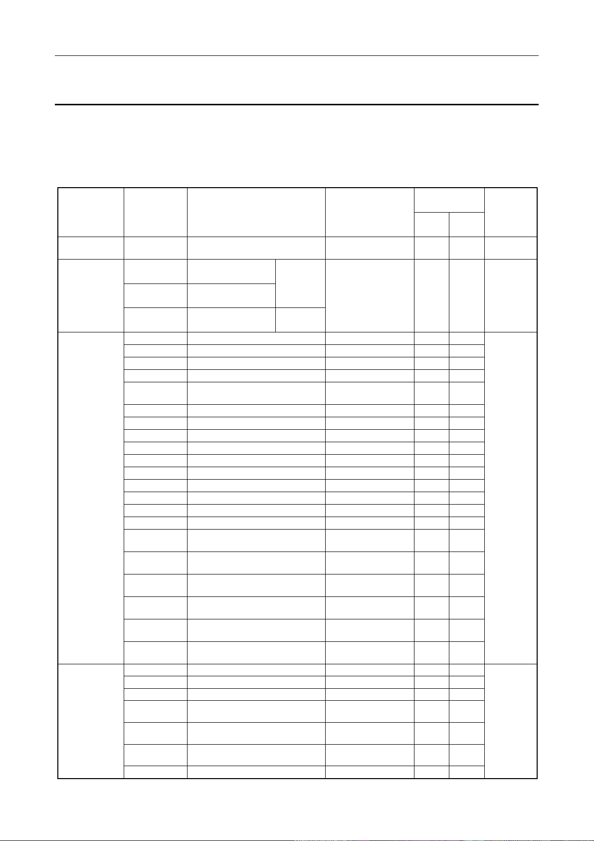
2.3 System Equipment
Various components of each module and peripheral device which can be used by the A2USHCPU-S1
are listed.
(1) Modules dedicated to A1S
Item Model Description
CPU module A2USHCPU-S1
A1S61PN 5VDC, 5A
Power supply
module
Input module
Output module
A1S62PN 5VDC, 3A/24VDC, 0.6A
A1S63P 5VDC, 5A 24VDC input
A1SX10 16-point 100 to 120 VAC input module 16 [16 input points] 0.05
A1SX10EU 16-point 100 to 120 VAC input module 16 [16 input points] 0.05
A1SX20 16-point 200 to 240 VAC input module 16 [16 input points] 0.05
A1SX20EU 16-point 200 to 240 VAC input module 16 [16 input points] 0.05
A1SX30
A1SX40 16-point 12/24VDC input module 16 [16 input points] 0.05
A1SX40-S1 16-point 24VDC input module 16 [16 input points] 0.05
A1SX40-S2 16-point 24VDC input module 16 [16 input points] 0.05
A1SX41 32-point 12/24VDC input module 32 [32 input points] 0.08
A1SX41-S1 32-point 24VDC input module 32 [32 input points] 0.12
A1SX41-S2 32-point 24VDC input module 32 [32 input points] 0.08
A1SX42 64-point 12/24VDC input module 64 [64 input points] 0.09
A1SX42-S1 64-point 24VDC input module 64 [64 input points] 0.16
A1SX42-S2 64-point 24VDC input module 64 [64 input points] 0.09
A1SX71 32-point 5/12/24VDC input module 32 [32 input points] 0.075
A1SX80
A1SX80-S1
A1SX80-S2
A1SX81
A1SX81-S2
A1SX82-S1
A1SY10 16-point relay contact output module (2A) 16 [16 output points] 0.12 0.09
A1SY10EU 16-point relay contact output module (2A) 16 [16 output points] 0.12 0.09
A1SY14EU 12-point relay contact output module (2A) 16 [16 output points] 0.12 0.10
A1SY18A
A1SY18AEU
A1SY22 16-point Triac output module (0.6A) 16 [16 output points] 0.27
A1SY28EU 8-point Triac output module (0.6A) 16 [16 output points] 0.27
1024 real I/O points, 256k bytes memory
capacity
16-point 12/24VDC, 12/24VAC input
module
16-point 12/24VDC sink/source input
module
16-point 24VDC sink/source input
module
16-point 24VDC sink/source input
module
32-point 12/24VDC sink/source input
module
32-point 24VDC sink/source input
module
64-point 24VDC sink/source input
module
8-point relay contact output module (2A)
for independent contacts
8-point relay contact output module (2A)
for independent contacts
100/200VAC
input
Number of occupied
points (points)
[I/O alloc a t ion module
type]
0.32
16 [16 input points] 0.05
16 [16 input points] 0.05
16 [16 input points] 0.05
16 [16 input points] 0.05
32 [32 input points] 0.08
32 [32 input points] 0.08
64 [64 input points] 0.16
16 [16 output points] 0.24 0.075
16 [16 output points] 0.24 0.075
Current
consumption
5VDC
(A)
24VDC
(220VAC)
(A)
0.002
Remark
Built-in
RAM memory
Installed in the
power supply
slot of the
basic base
module and
expansion
base module.
2-8
Page 23
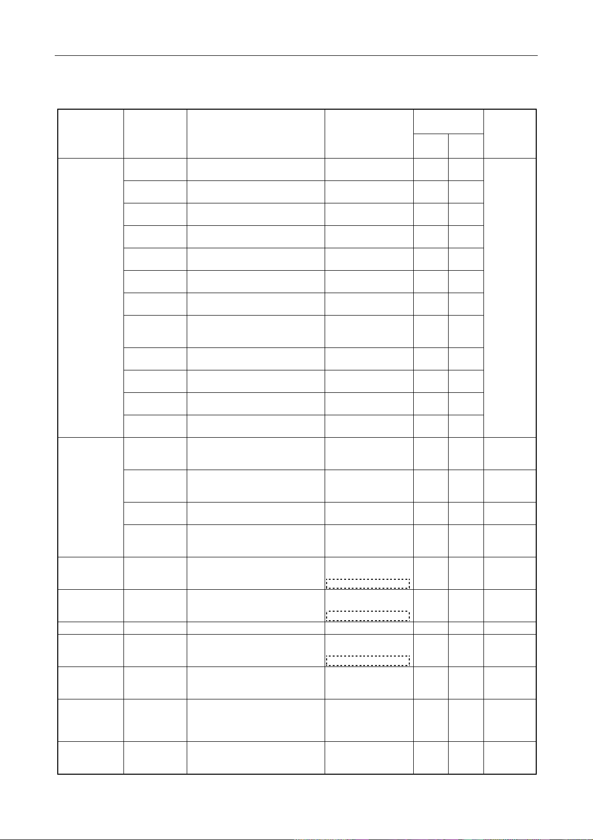
2. SYSTEM CONFIGURATION MELSEC-A
Number of occupied
Item Model Description
A1SY28A
A1SY40
A1SY41
A1SY42
A1SY50
A1SY60
Output module
I/O hybrid module
Dynamic input
module
Dynamic output
module
Blank cover A1SG60 Dust-proof cover for unused slot 16 [Empty]
Dummy module A1SG62
Pulse catch
module
Analog timer
module
Interrupt module A1SI61
A1SY60E
A1SY68A
A1SY71
A1SY80
A1SY81
A1SY82
A1SH42
A1SH42-S1
A1SX48Y18
A1SX48Y58
A1S42X
A1S42Y
A1SP60
A1ST60
8-point Triac output module (1A)
All points independent
16-point 12/24VDC transistor output
module(0.1A) sink type
32-point 12/24VDC transistor output
module(0.1A) sink type
64-point 12/24VDC transistor output
module(0.1A) sink type
16-point 12/24VDC transistor output
module(0.5A) sink type
16-point 24VDC transistor output
module(2A) sink type
16-point 5/12/24VDC transistor output
module(2A) source type
8-point 5/12/24/48VDC transistor output
module (2A) sink/source type
All points independent
32-point 5/12VDC transistor output
module(0.016A) sink type
16-point 12/24VDC transistor output
module(0.8A) source type
32-point 12/24VDC transistor output
module(0.1A) source type
64-point 12/24VDC transistor output
module(0.1A) source type
32-point 12/24VDC input module
32-point 12/24VDC transistor output
module(0.1A) sink type
32-point 24VDC input module
32-point 24VDC transistor output
module(0.1A) sink type
8-point 24VDC input module
8-point relay contact output module (2A)
8-point 24VDC input module
8-point 12/24VDC transistor output
module (0.5A)
16/32/48/64 points
12/24VDC dynamic input module
16/32/48/64 points
12/24VDC dynamic output module
16-point, 32-point, 48-point, or 64-point
selectable module
16-point input module for short ON-time
pulse input
(pulse with a minimum of 0.5ms)
8-point analog timer module whose
timer setting value can be changed f or
different volumes (0.1 to 1.0s, 1 to 10s,
10 to 60s, 60 to 600s)
Interrupt module for specifying the
interrupt program (16-point interrupt
input)
points (points)
[I/O alloc a t ion module
type]
16 [16 output points] 0.13
16 [16 output points] 0.27 0.008
32 [32 output points] 0.50 0.016
64 [64 output points] 0.93 0.008
16 [16 output points] 0.12 0.06
16 [16 output points] 0.12 0.015
16 [16 output points] 0.20 0.01
16 [16 output points] 0.11
32 [32 output points] 0.40 0.15
16 [16 output points] 0.12 0.02
32 [32 output points] 0.50 0.016
64 [64 output points] 0.93 0.008
32 [32 output points] 0.50 0.008
32 [32 output points] 0.50 0.008
16 [16 output points] 0.085 0.045
16 [16 output points] 0.06 0.06
Specified number of
points [Input
specified number of points]
Specified number of
points [Output
specified number of points]
Specified number of
points [Input
specified number of points]
16 [16 output points] 0.055
16 [16 output points] 0.055
32 [32 special points] 0.057
Current
consumption
5VDC
0.08
0.10 0.008
(A)
24VDC
(A)
Remark
2-9
Page 24

2. SYSTEM CONFIGURATION MELSEC-A
Item Model Description
32-bit signed binary
50kBPS, 1 channel
24-bit signed binary, 2 channels
100kPPS, DC input
Transistor output (sink type)
24-bit signed binary, 2 channels
200kPPS, difference input
Transistor output (sink type)
24-bit signed binary, 2 channels
200kPPS, difference input
Transistor output (sink type)
24-bit signed binary, 2 channels
100kPPS, DC input
Transistor output (source type)
4 to 20mA/0 to 10V
4 analog channels
4 to 20mA/0 to 10V
8 analog channels
For Pt100 (3-wire type) connection
2 channels of temperature input
For Pt100 (4-wire type) connection
2 channels of temperature input
4 to 20mA/0 to 10V
2 analog output channels
-10 to 10V input
Analog output, 8 channels
4 to 20mA input
Analog output, 8 channels
Analog input, 2 channels, simple loop
control is allowed.
Analog output, 1 channel
Analog input, 4 channels, simple loop
control is allowed.
Analog output, 2 channels
Thermocouple input - transistor input, 4
channels
Thermocouple input - transistor input, 4
channels
With disconnection det ec t ion f unction
Platinum resistance temperature sens or
input - transistor input, 4 channels
Platinum resistance temperature sens or
input - transistor input, 4 channels
With disconnection det ec t ion f unction
Thermocouple input - transistor output
(overheat cooling), 2 channels
Thermocouple input - transistor output
(overheat cooling), 2 channels
With disconnection det ec t ion f unction
Platinum resistance temperature sens or
input - transistor output (heat cooling), 2
channels
High-speed
counter module
A/D converter
module
Temperature/
digital converter
module
D/A converter
module
Analog I/O module
Temperature
regulating module
A1SD61
A1SD62
A1SD62D
A1SD62D-S1
A1SD62E
A1S64AD
A1S68AD
A1S62RD3N
A1S62RD4N
A1S68TD Thermocouple input, 8 channels 32 [32 special points] 0.32
A1S62DA
A1S68DAV
A1S68DAI
A1S63ADA
A1S66ADA
A1S64TCTT-S1
A1S64TCTTBWS1
A1S64TCRT-S1
A1S64TCRTBWS1
A1S62TCTT-S2
A1S62TCTTBWS2
A1S62TCRT-S2
Number of occupied
points (points)
[I/O alloc a t ion module
type]
32 [32 special points] 0.35
32 [32 special points] 0.1
32 [32 special points] 0.25
32 [32 special points] 0.27
32 [32 special points] 0.1
32 [32 special points] 0.4
32 [32 special points] 0.4
32 [32 special points] 0.49
32 [32 special points] 0.39
32 [32 special points] 0.8
32 [32 special points] 0.65
32 [32 special points] 0.85
32 [32 special points] 0.8
32 [32 special points] 0.21 0.16
32 [32 special points] 0.33
32 [32 special points] 0.42
32 [32 special points] 0.33
32 [32 special points] 0.42
32 [32 special points] 0.19
32 [32 special points] 0.28
32 [32 special points] 0.19
2-10
Current
consumption
5VDC
24VDC
(A)
(A)
Remark
Page 25

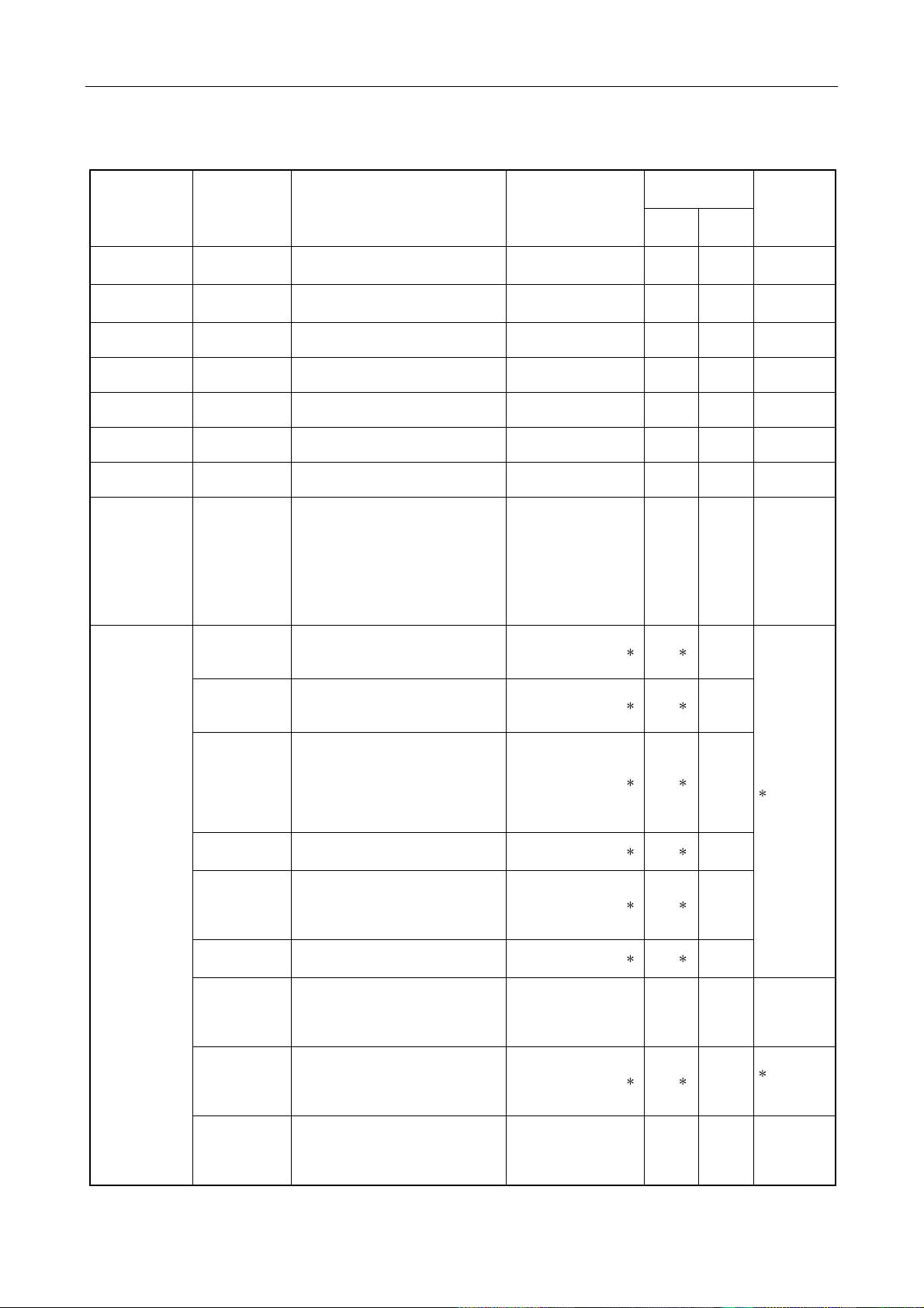
2. SYSTEM CONFIGURATION MELSEC-A
Item Model Description
Platinum resistance temperature sens or
Temperature
regulating module
Computer link
module
Ethernet interface
module
Intelligent
communication
module
Positioning module
A1S62TCRTBWS2
A1SJ71UC24-R2
A1SJ71UC24PRF
A1SJ71UC24-R4
A1SJ71E71N-B2 10 Base 2 (for Cheapernet) 32 [32 special points] 0.64
A1SJ71E71N-B5T 10 Base 5 (for Ethernet), 10 Base T 32 [32 special points] 0.42
A1SD51S
A1SD70
A1SD71-S2
A1SD71-S7
A1SD75P1-S3
A1SD75P2-S3
A1SD75P3-S3
A1SD75M1
A1SD75M2
A1SD75M3
input - transistor output (heat cooling), 2
channels
With disconnection det ec t ion f unction
Computer link function
RS-232C, 1 channel
Computer link function, printer function
RS-232C, 1 channel
Computer link function, multidrop link
function RS-422/RS-485, 1 channel
BASIC (interpreter/compiler)
RS-232C, 2 channels
RS-422/485, 1 channel
Analog voltage output (0 to ±10V) for 1-
axis positioning control, speed
control, and speed-positioning control.
For positioning control, speed control,
and speed-positioning control.
Pulse train output, 2-axis (independent,
2-axis simultaneous, linear
interpolation
For positioning control, setting for
manual pulse output speed can be
changed.
Pulse train output, 2-axis (independent,
2-axis simultaneous, linear interpolation)
For positioning control, pulse output, 1axis
For positioning control, pulse output, 2axis (independent, 2-axis simultaneous,
linear interpolation, circular interpolation)
For positioning control, pulse output, 3axis (independent, 3-axis simultaneous,
2-axis linear interpolation, 2-axis circular
interpolation)
For positioning control, digital output, for
MR-H-B/MR-J-B/MR-J2-B, 1-axis SSCNET
For positioning control, digital output, for
MR-H-B/MR-J-B/MR-J2-B, 2-axis SSCNET
(independent, 2-axis simultaneous,
linear interpolation, circular interpolation)
For positioning control, digital output, for
MR-H-B/MR-J-B/MR-J2-B, 3-axis SSCNET
(independent, 3-axis simultaneous, 2axis linear interpolation, 2-axis circular
interpolation)
Number of occupied
points (points)
[I/O alloc a t ion module
type]
32 [32 special points] 0.28
32 [32 special points] 0.1
32 [32 special points] 0.1
32 [32 special points] 0.1
32 [32 special points] 0.4
48 [First half: 16 empty
points]
[Second half: 32 special
points]
32 [32 special points] 0.7
32 [32 special points] 0.7
32 [32 special points] 0.7
32 [32 special points] 0.7
32 [32 special points] 0.7
32 [32 special points] 0.7
Current
consumption
5VDC
24VDC
(A)
0.3
0.8
0.8
(A)
Remark
Only AnACPUequivalent
device range
accessibleFil
e register and
program
read/write
disabled.
When
differential
driver is
connected
: 0.78
2-11
Page 26

2. SYSTEM CONFIGURATION MELSEC-A
Item Model Description
ID interface module
ID interface
module
MELSECNET(II)
data link module
MELSECNET/B
data link module
B/NET data link
module
MELSECNET/10
data link module
CC-Link system
master module
MELSECNET
/MINI-S3 master
module
MELSECNET-I/O
LINK master
module
S-LINK interface
module
JEMANET (JPCN-
1) interface module
DeviceNet
interface module
A1SD35ID1
A1SD35ID2
A1SJ71AP21
A1SJ71AP21-S3
A1SJ71AR21
A1SJ71AT21B
A1SJ72T25B
A1SJ71B62-S3
A1SJ71LP21
A1SJ71BR11
A1SJ71LR21
A1SJ61BT11
A1SJ71PT32-S3
A1SJ71T32-S3
A1SJ51T64
A1SJ71SL92N
A1SJ71J92-S3 JEMANET (JPCN-1) master module 32 [32 special points] 0.40
A1SJ72J95 JEMANET (JPCN-1) slave module 32 [32 special points] 0.40
A1SJ71DN91
One reader/writer module can be
connected.
ID interface module
Two reader/writer modules can be
connected.
For the master and local stations of
MELSECNET(II) data link system (for
the optical fiber cable)
For the master and local stations of
MELSECNET(II) data link system (for
the GI-type optical fiber cable)
For the master and local stations of
MELSECNET(II) data link system (for
the coaxial cable)
For the master and local stations of
MELSECNET/B data link system
For the remote I/O station of
MELSECNET/B data link system
Master module for B/NET
For the control, master, and normal
stations of the MELSECNET/10 data link
module system (For the dual loop SItype optical fiber cable)
For the control, master, and normal
stations of the MELSECNET/10 data
link module system (For the single bus
coaxial cable)
For the control, master, and normal
stations of the MELSECNET/10 data
link module system (For the single bus
coaxial cable)
(For the coaxial cable dual loop)
For the master and local stations of the
CC-Link data link system(For the twisted
pair shield cable only.)
For MELSECNET/MINI-S3 master
stations (max. 64 stations). Performs
remote I/O and remote terminal control
of a total of 512 I/O points.
MELSECNET/MINI-S3 master station
Performs remote I/O and remote
terminal control of a maximum 64
stations and a total of 512 I/O
points.(For the twisted pair cable only.)
MELSECNET-I/O LINK master station.
Controls I/O LINK remote I/O module of
a maximum of 64 stations and a total of
128 I/O points.
Master module for S-LINK
I/O total 128 points
Master module for DeviceNet
I/O total 4096 points
Number of occupied
points (points)
[I/O alloc a t ion module
Expanded mode 48 [48
Expanded mode 48 [48
type]
32 [32 special points] 0.25 0.17
32 [32 special points] 0.25 0.33
32 [32 special points] 0.33
32 [32 special points] 0.33
32 [32 special points] 0.8
32 [32 special points] 0.66
0.3
32 [32 special points] 0.08
32 [32 special points] 0.65
32 [32 special points] 0.80
32 [32 special points] 1.14
32 [32 special points] 0.40
I/O dedicated mode 32
[32 special points]
special points]
I/O dedicated mode 32
[32 special points]
special points]
64 [64 output points] 0.115 0.09
32 [32 special points] 0.20
32 [32 special points] 0.24
Current
consumption
5VDC
0.35
0.30
24VDC
(A)
(A)
Remark
Access is
allowed within
the device
range of the
A3ACPU.
Accessible
only within
MELSECNET
(II) range
2-12
Page 27
2. SYSTEM CONFIGURATION MELSEC-A
Item Model Description
PROFIBUS-DP
slave module
AS-I interface
module
Modem interface
module
Paging interface
module
Position detection
module
PC easier
monitoring module
Memory card
interface module
Simulation module A6SIM-X64Y64
Graphic operation
terminal
A1SJPB93D
A1SJ71AS92
A1SJ71CMO-S3 Modem interface module 32 [32 special points] 0.26
A1SD21-S1 Paging interface module 32 [32 special points] 0.14
A1S62LS Absolute position detection module 32 [32 special points] 0.55
A1SS91 PC easier monitoring module 32 [32 special points] 0.08
A1SD59J-S2 Memory card interface module 32 [32 special points] 0.05
A985GOT
A975GOT
A970GOT
A960GOT
A956GOT
A956WGOT
A953GOT
A951GOT
A950GOT
Slave module for PROFIBUS-DP
I/O data total 192 words
Master module for AS-I
I/O total 496 points
An I/O simulation unit used connected to
the base module. Debugging can be
executed without connecting the I/O
module to the base module.
Use an expansion cable of the AnS
series between the basic base module
of the AnS series and the A6SIMX64Y64.
Large-size graphic operation terminal
256 colors, TFT color, 800 × 600 dots,
high intensity
Large-size graphic operation terminal
256 colors, TFT color, 640 × 480 dots,
high intensity
Large-size graphic operation terminal
16 colors, TFT color, 640 × 480 dots,
high intensity/16 colors, TFT color, 640
480 dots, wide viewing angle/8 colors,
×
STN color, 640 × 480 dots/2 colors, STN
monochrome, 640 × 480 dots
Large-size graphic operation terminal
2 colors, EL, 640 × 400 dots
Medium-size graphic operation terminal
8 colors, STN color, 320 × 240 dots/STN
monochrome, 320 × 240 dots/256
colors, TFT color, 320 × 240 dots
Medium-size graphic operation terminal
256 colors, TFT color, 480 × 234 dots
Medium-size graphic operation terminal
8 colors, STN color, 320 × 240 dots/STN
monochrome, 320 × 240 dots/256
colors, TFT color, 320 × 240 dots
Medium-size graphic operation terminal
8 colors, STN color, 320 × 240 dots/STN
monochrome, 320 × 240 dots/256
colors, TFT color, 320 × 240 dots
Medium-size graphic operation terminal
8 colors, STN color, 320 × 240 dots/STN
monochrome, 320 × 240 dots/256
colors, TFT color, 320 × 240 dots
Number of occupied
points (points)
[I/O alloc a t ion module
32 [32 special points] 0.22
32 [32 special points] 0.22
32 [32 special points]
32 [32 special points]
32 [32 special points] 0.22
32 [32 special points] 0.22
32 [32 special points] 0.22
type]
32 [32 special points] 0.36
32 [32 special points] 0.15
64 [64 input points]
64 [64 output points]
Current
consumption
5VDC
(A)
TYP. 0.3
(when all
points
“ON”.)
0.22
0.22
24VDC
(A)
Remark
When bus connected
For RS-232C
connected
only
When bus connected
For RS-422
connected
only
2-13
Page 28
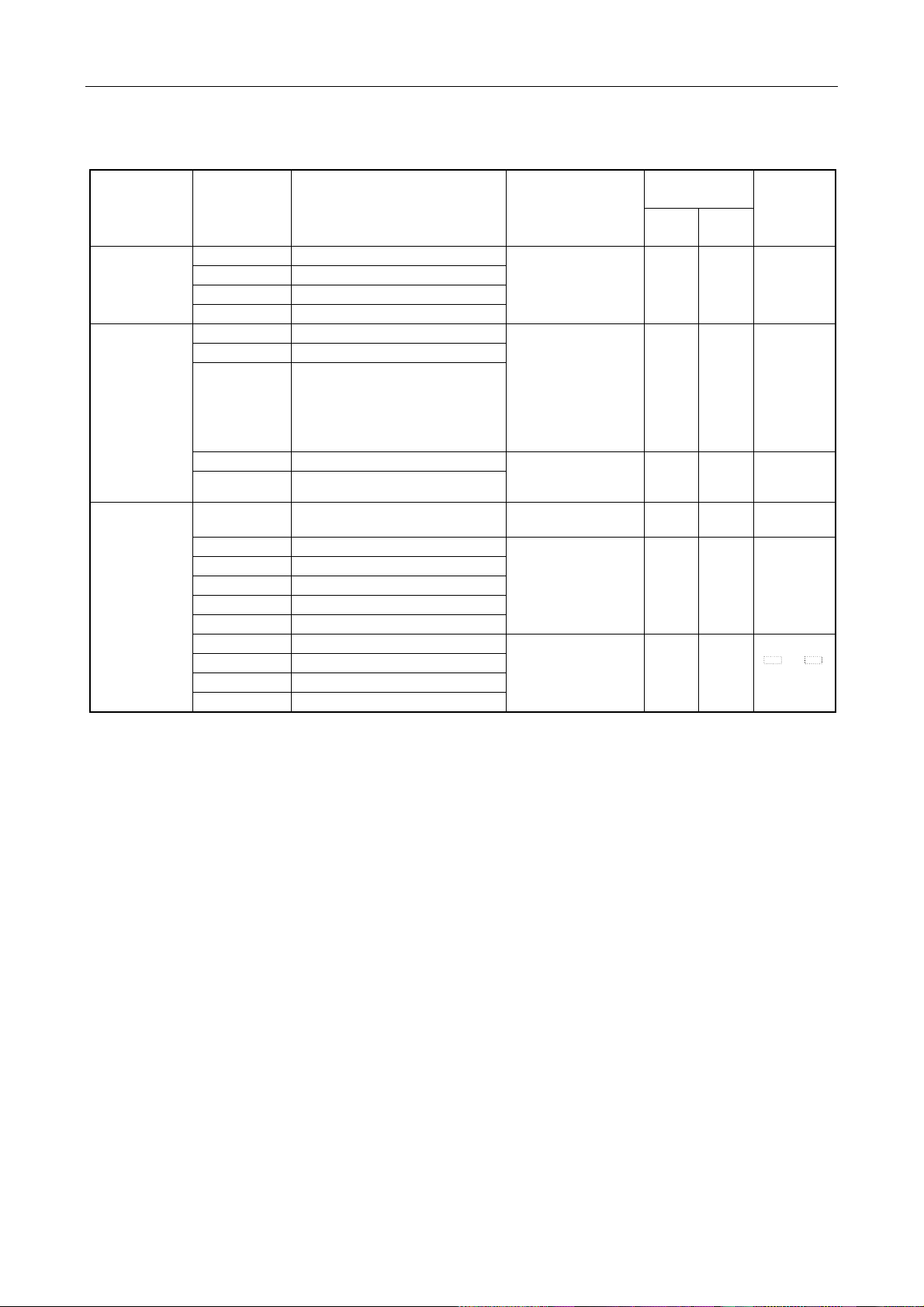
2. SYSTEM CONFIGURATION MELSEC-A
Item Model Description
A1S32B 2 I/O module can be installed.
Basic base unit
Extension base
unit
Extension cable
A1S33B 3 I/O module can be installed.
A1S35B 5 I/O module can be installed.
A1S38B 8 I/O module can be installed.
A1S52B 2 I/O module can be installed.
A1S55B 5 I/O module can be installed.
A1S58B 8 I/O module can be installed.
A1S65B 5 I/O module can be installed.
A1S68B 8 I/O module can be installed.
A1SC01B 55mm (2.17 in.) long flat cable
A1SC03B 330mm (13 in.) long
A1SC07B 700mm (27.56 in.) long
A1SC12B 1200mm (47.24 in.) long
A1SC30B 3000mm (118.11 in.) long
A1SC60B 6000mm (236.22 in.)long
A1SC05NB 450mm (17.72 in.)long
A1SC07NB 700mm (27.56 in.) long
A1SC30NB 3000mm (118.11 in.) long
A1SC50NB 5000mm (196.86 in.) long
Number of occupied
points (points)
[I/O alloc a t ion module
type]
Current
consumption
5VDC
(A)
24VDC
(A)
Remark
Extension
connector on
the right and
left side each.
The power
supply module
cannot be
installed.
(Power is
supplied from
the basic base
module.)
The power
supply module
is required.
For extension
towards right.
Connection
cable for the
extension
base module.
Cable for the
N, A A
A
extension
base module.
2-14
Page 29
2. SYSTEM CONFIGURATION MELSEC-A
Item Model Contents Applicable models
Memory
cassette
EPROM
E
Memory write adapter A2SWA-28P
Battery A6BAT IC-RAM memory backup Installed in the A2USHCPU-S1 main module
Connector/terminal
block converter unit
Cable for the
connector/terminal
block converter unit
Relay terminal unit A6TE2-16SRN For the sink-type output m odule A1SY41, A1SY42, A1SH42(S1)
Cable for connecting
the relay terminal unit
Terminal block cover
for the A1S I/O
module and the
special module
Insulation
displacement terminal
block adapter
Terminal block
adapter
40-pin connector
37-pin D-sub
connector
A2SMCA-14KP With a 14k-step EPROM (direct connection) A2SWA-28P is required
2
PROM
A2SNMCA30KE
A6TBXY36
A6TBXY54
With a 30k-step E
PROM (direct
connection)
Adapter for the memory cassette
attachment connector/28-pin EPROM
For the sink-type input module and sinktype output module. (standard type)
For the sink-type input module and sinktype output module. (2-wire type)
Direct writing to and reading from a peripheral device is
feasible.
Used for the ROM writing of A2SMCA-I4KP
A1SX41(S1/S2), A1SX42(S1/S2), A1SY41, A1SY42,
A1SY82, A1SH42(S1)
2
A6TBX70 For the sink-type input module. (3-wire type) A1SX41(S1/S2), A1SX42(S1/S2), A1SH42(S1)
A6TBX36-E
A6TBY36-E
A6TBX54-E
A6TBY54-E
A6TBX70-E
For the source-type input module. (standard
type)
For the source-type output module.
(standard type)
For the source-type input module. (2-wire
type)
For the source-type output module. (2-wire
type)
For the source-type input module. (3-wire
type)
A1SX81(S2), A1SX71, A1SX82-S1
A1SY81, A1SY82
A1SX81(S2), A1SX71, A1SX82-S1
A1SY81, A1SY82
A1SX81(S2), A1SX71, A1SX82-S1
AC05TB 0.5m (1.64 ft.) for the source module
AC10TB 1m (3.28 ft.) for the source module
AC20TB 2m (6.56 ft.) for the source module
AC30TB 3m (9.84 ft.) for the source module
AC50TB 5m (16.40 ft.) for the source module
A6TBXY36
A6TBXY54
A6TBX70
AC80TB 8m for the sink module
AC100TB 10m for the sink module
AC05TB-E 0.5m (1.64 ft.) for the source module
AC10TB-E 1m (3.28 ft.) for the source module
AC20TB-E 2m (6.56 ft.) for the source module
AC30TB-E 3m (9.84 ft.) for the source module
AC50TB-E 5m (16.40 ft.) for the source module
A6TBX36-E
A6TBY36-E
A6TBX54-E
A6TBY54-E
A6TBX70-E
AC06TE 0.5m (1.64 ft.) long
AC10TE 1m (3.28 ft.) long
AC30TE 3m (9.84 ft.) long
A6TE2-16SRN
AC50TE 5m (16.40 ft.) long
AC100TE 10m (32.81 ft.) long
Slim-type terminal block cover for t he A1S
A1STEC-S
I/O module and the special module
All terminal block connector type modules
(terminal block type).
A1S-TA32
A1S-TA32-3
A1S-TA32-7
A1S-TB32
Insulation displacement terminal block
adapter for 32 points 0.5mm
Insulation displacement terminal block
adapter for 32 points 0.3mm
Insulation displacement terminal block
adapter for 32 points 0.75mm
2
(AWG20)
2
(AWG22)
2
(AWG18)
For 32 points, conversion into Europe type
terminal block
A1SX41(S1/S2), A1SX71, A1SY41, A1SY71
A1SX41(S1/S2), A1SX71, A1SY41, A1SY71
A6CON1 Soldering type, straight out
A6CON2 Solderless type, straight out
A6CON3 Press-fit type, flat cable
Sink type (40p FCN)
A6CON4 Soldering type, straight/diagonal out
A6CON1E Soldering type, straight out
A6CON2E Solderless type, straight out
Source type (37p D-sub)
A6CON3E Press-fit type, flat cable
2-15
Page 30
2. SYSTEM CONFIGURATION MELSEC-A
(2) Peripheral devices
Item Model Remark
A6PHP main module
•
SW
Plasma hand-held
graphic programmer
Intelligent GPP A6GPP-SET
Composite video
cable
RS-422 cable
User floppy disk SW0-GPPU 2DD-type
Cleaning floppy disk SW0-FDC For A6GPP/A6PHP Floppy disk for cleaning the floppy disk drive.
Optional keyboard for
A6PHP
Optional keyboard for
A6GPP
Printer
RS232C cable AC30R2
Printer paper
Inked ribbon for
K6PR(K)
Inked ribbon for
A7NPR-S1
Programming module
A6PHP-SET
AC10MD
AC30R4 3m (9.84 ft.) long
AC300R4 30m (98.43 ft.) long
A6KB-SET-H
A6KB-SET
K6PR-K
A7NPR-S1
K6PR-Y
K7PR-Y
K6PR-R Replacement inked ribbon for K6PR-K.
A7NPR-R Replacement inked ribbon for A7NPR-S1.
A7PUS
A8PU
A8UPU
•
•
•
•
•
•
•
•
•
•
•
•
•
•
•
•
•
Connection cable for between A6GPP/A6PHP and printer (K6PR-K,
A7NPR-S1, and a general-purpose printer with RS-232C interface)
3m (9.84 ft.) long
Printer paper for K6PR(S1) and K6PR-K. 9-inch paper. 2000 sheets per
unit.
Printer paper for A7PR and A7NPR. 11-inch paper. 2000 sheets per unit.
Read/write of the program is performed by connecting to the CPU main
module with a RS-422 cable (AC30R4-PUS). (5VDC 0.4A)
Read/write of the program is performed by connecting to the CPU main
module with a RS-422 cable (AC30R4-PUS, AC20R4-A8PU). (5VDC 0.4A)
GP-GPPA....... GPP function startup floppy disk for the A series.
SW
GP-GPPK....... GPP function startup floppy disk for the K series.
SW0-GPPU ............... User floppy disk (2DD).
AC30R4..................... 3m (9.84 ft.)-long RS-422 cable.
A6GPP main module
GP-GPPA....... GPP function startup floppy disk for the A series.
SW
SW
GP-GPPK....... GPP function startup floppy disk for the K series.
SW0-GPPU ............... User floppy disk (2DD).
AC30R4..................... 3m (9.84 ft.)-long RS-422 cable.
Connection cable for the monitor display of the A6GPP screen.
1m (3.28 ft.)long
Connection cable for between the CPU main
module and A6GPP/A6PHP
Floppy disk for storing user programs (3.5-inch, preformatted)
A6KB keyboard
AC03R4H .....0.3m (0.98 ft.)-long connection cable between A6KB and
A6PHP.
A6KB-C ........Key sheet for the GPP mode of A6KB.
A6KB keyboard
AC03R4L...... 0.3m (0.98 ft.)-long connection cable between A6KB and
A6GPP.
A6KB-C Key sheet for the GPP mode of A6KB.
For printing out program circuit diagrams and various lists.
2-16
Page 31

2. SYSTEM CONFIGURATION MELSEC-A
Item Model Remark
Connection cable for between the CPU main module and A7PUS, A8PU,
AC30R4-PUS
RS-422 cable
AC20R4-A8PU
P-ROM write module A6WU
Data access module A6DU-B
Modem interface
module
RS-422 cable
A6TEL
AC30R4
AC300R4
AC03WU
A8UPU.
3m (9.84 ft.) long
Connection cable for between the CPU main module and A8PU, A8UPU.
2m (6.56 ft.) long
Used to write the program in the CPU/A6PHP main module to a ROM, or
•
to read out the program in the ROM for the CPU main module.
Connect to the CPU/A6PHP with an AC30R4/AC03WU cable.
•
Used for monitoring the CPU devices, changing the s et t ing values/
•
current values, and displaying the operation st at us . (5VDC 0.23A)
Connect to the CPU with an AC30R4-PUS cable.
•
An interface module which connects the PC CPU and the modem. Using
•
a telephone line, the communication is perform ed bet ween a remote
peripheral device and the CPU. (5VDC 0.2A)
Connect to the CPU with an AC30R4-PUS cable.
•
Connection cable for between the CPU main module and A6WU. 3m/30m
(9.84 ft./98.43 ft.) long.
Connection cable for between the A6PHP main module and A6WU. 0.3m
(0.98 ft.) long.
2-17
Page 32

2. SYSTEM CONFIGURATION MELSEC-A
2.4 System Configuration Overview
There are four system configuration types as follows:
Stand-alone system
(1) --
Network system
(2) --
Computer link system
(3)
Composite system
(4)
The details of the system configuration, number of I/O points, I/O number assignment, etc., of a
stand-alone system are listed on the following page.
............. A system with a basic base module only, or with a basic base
system and an extension base module connected with the
expansion cable.
.................... A system for controlling multiple PCs and remote I/O modules.
.......... A system for data exchange between the A2USHCPU-S1 and the
computer (personal computer, etc.) by using an A1SJ71UC24
computer link module.
............... A system which has a combination of a network system and a
computer link system.
2-18
Page 33

2. SYSTEM CONFIGURATION MELSEC-A
A2USHCPU-S1 system
System
configuration
[When the A1S dedicated extension bas e is us ed]
An example when a 64-point module is installed to each
slot is shown.
Basic base
Slot number
0
1
2
3
4
5
6
7
00
40
80
C0
100
140
180
17F
1C0
to
to
to
1BF
1FF
to
to
to
3F
7F
BF
to
to
FF
13F
[When the AcN or AcA extension base is used]
An example when a 64-point module is installed to each
slot is shown.
Basic base
Slot number
0
1
2
3
4
5
6
7
00
40
80
C0
100
140
180
17F
1C0
to
to
to
1BF
1FF
to
to
3F
7F
BF
to
to
to
FF
13F
UNIT
1
2
3
4
5
6
7
Extension cable
8
200
to
23F
Slot number
9
10
240
280
to
to
27F
2BF
11
2C0
2FF
Extension cable
Slot number
8
9
200
240
to
to
23F
27F
10
280
to
2BF
11
12
13
14
15
2C0
300
340
380
to
to
2FF
33F
to
37F
3C0
to
to
3BF
3FF
1st extension
1
2
3
4
5
6
7
Extension base (A N, A A)
Maximum number
of extension
Maximum number
of I/O modules
Maximum number
of I/O points
Basic base unit
model
Extension base unit
model
Extension cable
model
Extension base (For A1S only)
1 extension unit 1 extension unit
A1S32B, A1S33B, A1S35B, A1S38B
A1S65B, A1S68B, A1S52B, A1S55B, A1S58B A62B, A65B, A68B, A52B, A55B, A58B
A1SC03B, A1SC07B, A1SC12B, A1SC30B,
A1SC01B (right-side installation), A1SC60B
16 modules
1024 points
A1SC05NB. A1SC07NB
A1SC30NB, A1SC50NB
Notes (1) Only one extension base module can be used. (The second extension module cannot be used.)
(2) When the extension base A1S52B, A1S55B, A1S58B, A55B or A58B is used, the 5VDC power is supplied from the
power supply module of the basic base module. Before use, refer to Sect ion 6. 1. 3 and examine if it c an be us ed.
(3) Limit the length of extension cable to 6m or short er.
(4) If an extension cable is used, do not tie it with the main circuit cables, which has high voltage, large current, or
install them close to each other.
Assignment of the
I/O numbers
(When I/O is not
assigned)
(1) Assign I/O numbers to the basic base unit first, then to the extension base unit.
(2) Assign I/O numbers as if both basic bas e unit and extension base unit have 8 slots each. When the
A1S32B/A1S33B/A1S35B for 2/3/5 slots are used as the basic base unit, add 6/5/3 slots (96 points/48 points) and
assign the extension base unit I/O numbers.
(3) 16 points are assigned to an empty slot.
(4) When an extension base unit for A
N or A A is used, be sure to set to a single extension level. If it is set to
the number of skipped unit, 16 points/slot are assigned to all of "skipped unit x 8 slots", and thus it does not work.
(5) Items (2) to (4) can be changed by the I/O ass ignm ent . Refer t o t he ACPU Programm ing M anual (Fundament als )
for details.
12
13
14
15
300
340
380
to
37F
3C0
to
to
3BF
3FF
to
to
33F
2-19
Page 34

3. GENERAL SPECIFICATION MELSEC-A
3. GENERAL SPECIFICATION
The general specification common to various modules is shown.
Table 3.1 General specification
Item Specification
Operation ambient
temperature
Storage ambient
temperature
Operation ambient
humidity
Storage ambient
humidity
When there is intermitt ent vibration
Frequency Acceleration Amplitude Sweep count
10 to 57Hz
Conforms to the JIS
Vibration durability
Shock durability Conforms to the JIS B 3502 and IEC 61131-2 (147 m/s2 ), 3 times each in 3 directions)
Operation
ambiance
Operation height *3 2000m(6562 ft.) or less
Installation area On the control panel
Over-voltage
category *1
Pollution level *2 2 or less
B 3502 and IEC
61131-2
57 to 150Hz 9.8m/s2
When there is continuous vibration
Frequency Acceleration Amplitude
10 to 57Hz
57 to 150Hz 4.9m/s
10 to 90%RH, no condensation
10 to 90%RH, no condensation
*1 Indicates the locat i on the device is connected, f rom the public cable network to the devi ce structure wiring
area
.
Category II applies to the devices to which the power is supplied from a fixed equipment.
Surge withstand voltage for devices with up to 300V of rated voltage is 2500V.
*2 This is an index which indicates the degree of conductive object generation in the envi ronment where the
device is used. Pollution level 2 is when only non-conductive pollution occurs. A temporary conductivity
caused by condensation m ust be expected occasionally.
*3 Do not use or store the PC in the environment where the pressure is higher than the at mospheric pressure
at sea level. Otherwise, m al function may result. To use the PC in high-pressure environment , contact your
nearest Mitsubishi represent at i ve.
0 to 55°C
-20 to 75°C
2
No corrosive gas
II or less
0.075mm
(0.003 in.)
0.035mm
(0.001 in.)
10 times each in X,
Y, and Z directions
(80 minutes)
3-1
Page 35

4. CPU MODULE MELSEC-A
4. CPU MODULE
4.1 Performance Specification
Performance specifications of A2USHCPU-S1 module are shown below.
Performance specifications
Item
Control method Repeated operation of stored program
I/O control method Refresh method
Program language
Processing speed
(sequence instructions)
(µs/step)
Sequence
instructions
Number of
instructions
(type)
Constant scan (ms)
(Program startup with a
constant time interval)
Memory capacity 256k bytes (built-in RAM)
Program
capacity
(steps)
I/O device points 8192 (X/Y0 to 1FFF)
I/O points 1024 (X/Y0 to 3FF)
Internal relay [M] (points) 7144 (M0 to M999, M 2048 t o M8191)
Latch relay [L] (points) 1048 (L1000 to L2047)
Step relay [S] (points) 0 (None for the initial s t at e)
Link relay [B] (points) 8192 (B0 to B1FFF)
Timer [T] (points)
Device points
Counter [C] (points)
Data register [D] (points) 8192 (D0 to D8191)
Link register [W] (point s) 8192 (W0 to W 1FFF)
Annunciator [F] (points) 2048 (F0 to F2047) Device for failure detection
File register [R] (points) 8192 (R0 to R8191) Points set by parameters
Basic and
application
instructions
Dedicated
instruction
Main sequence
program
Sub sequence
program
Relay Symbol Language, Logic Symbolic Language, MELSAP-II (SFC)
100ms timer (T0 to T199)........................Setting time: 0.1 to 3276.7s
•
10ms timer (T200 to T255) .....................Setting time: 0.01 to 327.67s
•
100ms retentive timer (none for initial).....Setting time: 0.1 to 3276.7s
•
Expansion timer (T256 to T2047).............Time set by word device (D, W,
•
Normal counter (C0 to C255)...................Setting range : 1 to 32767 times
•
Interrupt counter (none for initial).............C224 to C255 possible
•
Expansion counter (C256 to C1023)........Count value set by word device
•
Dedicated language for sequence control
10 to 190 (setup possible with 10ms units)
2048 (Default 256 points)
1024 (Default: 256 points)
Model
A2USHCPU-S1
0.09
25
233
204
Maximum 30k step
None
Total 8192 shared by M, L, S
R)
depending on setting
(D,W,R)
Remark
Partial direct input and output
possible by instruction
Setup to special register
D9020
A2SMCA-14KP/14KE
A2SNMCA-30KE (64k bytes)
installation possible
Set by parameters
Number of points which can be
used in a program
Number of points accessible
from I/O module
The range can be changed by
parameters.
The range and number of
points for use set by
parameters
(Refer to Section 4.2.1)
The range and number of
points for use set by
parameters
(Refer to Section 4.2.1)
4-1
Page 36

4. CPU MODULE MELSEC-A
Performance specifications (Continued)
Item
Accumulator [A] (points) 2(A0, A1)
Index register [V, Z]
(points)
Pointer [P] (points) 256 (P0 to P255)
Interrupt pointe r [I] ( p o i n ts) 32 (I0 to I31)
Special relay [M] (points) 256 (M9000 to M9255)
Device points
Special register [D]
(points)
Comment (points) Maxim um 4032 (Set with the unit of 64 points )
Expanded comment (points) Maximum 3968 (Set with the unit of 64 points)
Switch output mode from
STOP to RUN
Self-diagnosis function
Operation mode upon error Select stop or continue
RUN time startup method
Latch (power failure
compensation) range
Remote RUN/PAUS E contacts Possible to setup one contact point for each of RUN/PA US E from X0 to X1FFF. Set by pa r a meters
Title for printing registration YES (128 characters) Set by parameters
Keyword registration YES Set by parameters
I/O allocation Possible to register occupied I/O points and m odule m odel nam es .
Step operation Possible to execute or stop sequence program operations . Refer to Section 4.3.
Interrupt processing
Data link MELSECNET/10, MELSECNET(II)/B
Clock function
Allowable period of momentary
power failure
5VDC internal power
consumption (A)
Weight (kg(lb)) 0.46 (1.01)
External dimensions
(mm(inch))
Select either re-output the operation status bef ore s t opping (def ault ) or out put
Operation watching time monitor (watchdog timer fixed to 200ms)
Error detection in the memory, CPU, I/O, battery, etc.
(upon power supply on/power restoration after power failure, automatic restart
by turning the "RUN" switch of the CPU t o O N.)
(Possible to setup latch ranges for L, B, T, C, D, W)
Possible to operate an interrupt program by the interrupt module or c ons t ant
Year, month, day, hour, minute, second, day of the week
Precision -3.2 to +5.1s (TYP. +1.6s)/d at 0°C
-1.2 to +5.3s (TYP +2.2s)/d at 25°C
-8.2 to +3.5s (TYP -1.6s)/d at 55°C
14(V, V
after execution of operation.
(automatic detection of the leap year)
130 (5.12) × 54.5 (2.15) × 93.6 (3.69)
NOTE
When conventional system S/W packages and peripheral devices are used, be careful as the
usable ranges of devices are limited.
Details are provided in Section 2.2.3.
Model
A2USHCPU-S1
1
to V6, Z, Z1 to Z6)
256 (D9000 to D9255)
Initialization start
L1000 to L2047 (default)
period interrupt signal.
By power supply module Refer to Section 5.1.
0.32
Set by parameters
Set by parameters
Refer to Section 4.1.4 for
details.
Set by parameters
(refer to Section 4.2.1.)
Range set by parameters
Remark
4-2
Page 37

4. CPU MODULE MELSEC-A
4.1.1 Overview of operation processing
An overview of processing subsequent to starting power supply for A2USHCPU-S1 to execution of the
sequence program is explained.
A2USHCPU-S1's processing may be categorized roughly into the following four kinds:
(1) Initial processing
This is a preprocess to execute sequence operations, and is performed only once upon power-on
or reset.
(a) Resets the I/O module and initialize it.
(b) Initializes the range of data memory for which latch is not set up (sets the bit device to OFF
and the word device to 0).
(c) Allocates I/O address of the I/O module automatically based on the I/O module number or
the position of installation on the extension base module.
(d) Executes the check items for power-on and reset among the PC CPU's self-diagnosis items
(Refer to 4.1.4).
(e) For the control station of the MELSECNET/10 or the master station of MELSECNET (II)/B,
sets the network/link parameter information to the network/data-link module, and
commences the network communication/data link.
(2) Refresh processing of I/O module
Executes the refresh processing of I/O module. (Refer to the ACPU Programming Manual
(Fundamentals).)
(3) Operation processing of a sequence program
Executes a sequence program from step 0 to the END instruction written in the PC CPU.
(4) END processing
This is a post-process to finish one cycle of operation processing of the sequence program and to
return the execution of the sequence program to the step 0.
(a) Performs self-diagnosis checks, such as fuse blown, I/O module verification, and low
battery. (Refer to Section 4.1.4.)
(b) Updates the current value of the timer, sets the contact ON/OFF, updates the current value
of the counter and sets the contact to ON. (Refer to the ACPU Programming Manual
(Fundamentals).)
(c) Performs data exchange between PC CPU and computer link module when there is a data
read or write request from a computer link module. (A1SJ71UC24-R2, AJ71C24(S3),
AD51(S3), etc.)
(d) Performs the refresh processing when there is a refresh request from the network module or
link module.
(e) When the trace point setting of sampling trace is by each scan (after the execution of END
instruction), stores the condition of the device for which it is setup into the sampling trace
area.
4-3
Page 38

4. CPU MODULE MELSEC-A
Power-on
Initial processing
• Initialization of I/O module
• Initialization of data memory
• I/O address allocation of I/O module
• Self-diagnosis
• Set link parameter
Refresh processing of I/O module
(only when the I/O control is set up for the
refresh processing)
Operation processing of the sequence program
Step 0
to
Until the execution of END (FEN D) instruction
END processing
• Self-diagnosis
• Updating current value of the timer and
counter, and setting the contacts ON/OFF
• Communication with computer link module
• Link refresh processing
• Sampling trace processing
• MELSECNET/MINI-S3 automatic refresh
processing
Figure 4.1 A2USHCPU-S1 operation processing
4-4
Page 39

4. CPU MODULE MELSEC-A
4.1.2 Operation processing of RUN, STOP, PAUSE, and STEP RUN
The PC CPU has four kinds of operation states: RUN state, STOP state, PAUSE state, and step
operation (STEP RUN) state.
Operation processing of PC CPU in each operation state is explained.
(1) RUN state operation processing
(a) The repetition of sequence program operation in the order from step 0 → END (FEND)
instruction → step 0 is called the RUN state.
(b) When entering the RUN state, the output state escaped by STOP is output depending on
the output mode setting of parameter upon STOP → RUN.
(c) Processing time from switching from STOP to RUN until the startup of sequence program is
usually one to three seconds, yet it may vary depending on the system configuration.
(2) STOP state operation processing
(a) The termination of operation of the sequence program by the use of RUN/STOP key switch
or the remote STOP is called the STOP state. (Refer to Section 4.3.)
(b) When entering the STOP state, it escapes the output state and sets all output points to OFF.
Data memories except for output (Y) are retained.
(3) PAUSE state operation processing
(a) The termination of operation of sequence program while retaining output and data memories
is called the PAUSE state. (Refer to Section 4.3.)
(4) Step operation (STEP RUN) operation processing
(a) Step operation is an operation mode wherein operation processing of a sequence program
can be paused/resumed by each instruction from peripheral device(s). (Refer to Section
4.3.)
(b) Since an operation processing is paused while retaining the output and data memories,
condition of the execution can be confirmed.
4-5
Page 40

4. CPU MODULE MELSEC-A
(5) Operation processing of PC CPU when RUN/STOP key switch is operated
PC CPU operation
processing
RUN/STOP key
switch operation
RUN → STOP
STOP → RUN Starts.
Operation processing of
the sequence progra m
Executes up to the END
instruction, then stops.
External output
OS escapes the output
state, and sets all the output
points to OFF.
Determined by the output
mode of the parameter upon
STOP → RUN.
Maintains the condition
immediately prior to entering the
STOP state.
Starts operations from the
condition immediately prior to
entering the STOP state.
Data memories
(Y, M, L, S, T, C, D)
POINTS
Whether in the RUN, STOP or PAUSE state, PC CPU is performing the following:
Refresh processing of I/O module
•
Data communication with computer link module
•
Link refresh processing.
•
Thus, even in the STOP or PAUSE state, monitoring or testing I/O with peripheral devices,
reading or writing from a computer link module, and communication with other stations by
MELSECNET are possible.
Remark
4-6
Page 41

4. CPU MODULE MELSEC-A
4.1.3 Operation processing upon momentary power failure
The PC CPU detects a momentary power failure when input power voltage supplied to the power
supply module becomes lower than the specified range.
When the PC CPU detects a momentary power failure, following operation processing is performed.
(1) When a momentary power failure shorter than allowable period of momentary power failure
occurred:
(a) When a momentary power failure occurred, operation processing is interrupted while the
output state is retained.
(b) When the momentary power failure is reset, operation processing will be continued.
(c) When a momentary power failure occurred and the operation was interrupted, measurement
of the watchdog timer (WDT) continues. For instance, when the scan time is 190ms and a
momentary power failure of 15ms occurs, it causes the watchdog timer error (200ms).
Momentary power failure occurred Power supply restoration
END END END0
A2USHCPU-S1 interrupts the operation.
Operation processing upon momentary power failure
(2) When a momentary power failure longer than the allowable period of momentary power
failure occurred:
The PC CPU performs the initial start. The operation processing is the same as power-on or reset
operation with the reset switch.
4-7
Page 42
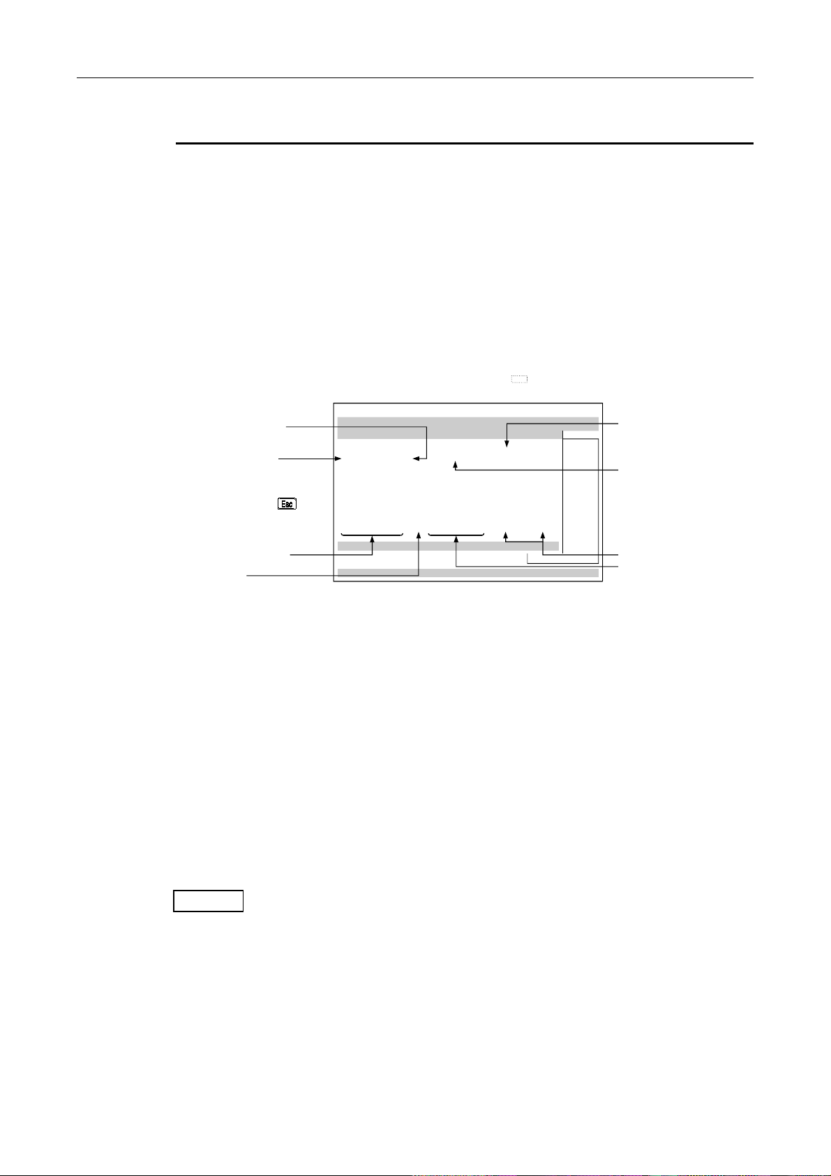
4. CPU MODULE MELSEC-A
4.1.4 Self-diagnosis
Self-diagnosis is a function with which A2USHCPU-S1 diagnoses itself for the presence of any
abnormalities.
(1) Upon turning on the power supply to PC or when an abnormality occurred while the PC is running,
the A2USHCPU-S1's self-diagnosis processing prevents malfunctions of the PC and performs
preventive maintenance by detecting the abnormality, displaying an error display, halting the
operation of A2USHCPU-S1, and so on.
(2) A2USHCPU-S1 stores the error occurred last to a special register D9008 as an error code, and
stores further detailed error code to a special register D9091.
(3) Even with the power-off, the latest error information and 15 errors in the past are stored by battery
back-up. With the AnUCPU-supporting system FD, contents of up to 16 errors can be confirmed
from the peripheral devices. Display example with SW
Displays the current error message.
Displays the current error number.
As the error generation condition, a maximum
of 16 latest errors are displayed with the time
of their occurrences.
The display is erased by pressing the key.
Displays the time and date of the occurrences
of errors.
(year, month, day, minutes, seconds)
Displays the error number.
(4) When the self-diagnosis detects an error, the module will be in one of the two modes below:
•
Mode wherein operation of the PC is stopped
•
Mode wherein operation of the PC continues
In addition, there are errors with which the operation can be selected to stop or to continue by the
parameter setting.
(a) When a stop-operation mode error is detected by the self-diagnosis, the operation is
stopped at the time of detection of the error, and sets the all outputs(Y) to OFF.
(b) When a continue-operation mode error is detected, the only part of the program with the
error is not executed while the all other part is executed. Also, in case of I/O module
verification error, the operation is continued using the I/O address prior to the error.
When an error is detected, error generation and error contents are stored in the special relay (M)
and special register (D), so that in case of the continue-operation mode, the program can use the
information to prevent any malfunctions of the PC or devices.
Error descriptions detected by the self-diagnosis are shown in the next page.
REMARK
1) As to the LED display message, the order of priority of the LED display can be changed if CPU is in
the operation mode. (An error code is stored in the special register).
2) When the special relay M9084 is ON, checking on blown fuse, I/O verification and the battery are
not performed (an error code is not stored in the special register).
3) The "Error display of peripheral device" in the table of self-diagnostic functions are messages
displayed by the PC diagnosis of peripheral devices.
PC A2A-FF-FC C:TEMP MAIN F11:MENU F12:HELP
<TEST>
<ERROR STATUS>
<CURRENT STATUS>
<ERROR MESSAGE>
70:BATTERY ERROR
<ERRORSTATUS>
<Y.M.D.H.M.S.>
01.01.12 17:05:14
01.01.14 05:16:45
01.01.15 00:11:34
01.01.15 11:06:33
01.01.15 21:39:12
01.01.18 08:58:22
01.01.18 09:28:22
Page Up Page Down Esc:CLOSE
<ERROR MESSAGE>
9: AC DOWN
9: AC DOWN
9: AC DOWN
9: AC DOWN
9: AC DOWN
9: AC DOWN
70: BATTERY DOWN
<DATA>
00000
<ERROR STEP>
IVD-GPPA is shown below:
RESULT
00000
<NO.2>
<NO.1>
00000
00000
00000
00000
00000
00000
00000
00000
00000
00000
00000
00000
00000
00000
Esc:Close
Displays the number of current
error steps.
Detailed error number
Displays number of error details
information.
Displays error message.
4-8
Page 43

4. CPU MODULE MELSEC-A
Self-diagnostic functions
Diagnosis item Diagnosis timing CPU status
Instruction code check Upon execution of each instruction INSTRCT. CODE ERR. 10
Upon power-on and reset
•
Parameter setting check
No END instruction
Unable to execute
instruction
Memory error
Format (CHK i n str u cti o n)
check
Unable to execute
instruction
RAM check
Operation circuit check • Upon power-on and reset OPE. CIRCUIT ERR. 21
Watchdog error
supervision
CPU error
END instruction not
executed
Main CPU chec k Always
Upon switching from (STOP, PAUSE) to
•
(RUN, STEP-RUN)
When M9056 or M9057 is ON
•
Upon switching from (STOP, PAUSE) to
•
(RUN, STEP-RUN)
CJ SCJ JMP CALL(P)
•
FOR to NEXT CHG
Upon execution of each instruction
Upon switching from (STOP, PAUSE) to
•
(RUN, STEP-RUN)
Upon switching from (STOP, PAUSE) to
(RUN, STEP-RUN)
When interruption occurred
•
Upon switching from (STOP, PAUSE) to
•
(RUN, STEP-RUN)
Upon power-on and reset
•
When M9084 is ON during STOP
•
Upon execution of END instruction WDT ERROR 22
•
Upon execution of END instruction END NOT EXECUTE 24
•
Stop Flickering
Stop Flickering
Status of
"RUN" LED
Error display of
peripheral devices
PARAMETER ERROR 11
MISSING END INS. 12
CAN’T EXECUTE (P) 13
CHK FORMAT ERR. 1 4
CAN’T EXECUTE (I) 15
RAM ERROR 20
MAIN CPU DOWN 26
Error code
(D9008)
I/O module verification
*1 (Default: stop)
I/O error
Fuse blown
*1 (Default: operate)
Control bus check Upon execut ion of FROM, TO inst ruc t ion CONTROL-BUS ERR. 40
Special function module
error
Link module error
I/O interrupt error W hen int errupt ion oc c ur I/O INT. ERROR 43
Special function module
allocation error
Special function module
error
Special function module error
*1 (Default: stop)
Link parameter error
Low battery
Battery
Upon execution of END instruction
(However, not checked when M9084 or
M9094 is ON.)
Upon execution of END instruction
(However, not checked when M9084 or
M9094 is ON.)
Upon execution of FROM, TO instruction SP. UNIT DOWN 41
Upon power-on and reset
•
Upon switching from (STOP, PAUSE) to
•
(RUN, STEP-RUN)
Upon power-on and reset
•
Upon switching from (STOP, PAUSE) to
•
(RUN, STEP-RUN)
Upon execution of FROM, TO instructions
Upon power-on and reset
•
Upon switching from (STOP, PAUSE) to
•
(RUN, STEP-RUN)
Always
(However, not checked when M9084 is
ON.)
Stop
Operate ON FUSE BREAK OFF. 32
Stop Flickering
Stop Flickering SP. UNIT ERROR 46
Stop
Operate ON
Operate Flickering BATTERY ERROR 70
Flickering
Flickering
UNIT VERIFY ERR. 31
LINK UNIT ERROR 42
SP. UNIT LAY. ERR. 44
LINK PARA. ERROR 47
Operation check error
*1 (Default: operate)
Upon execution of each instruction
Stop
Operate ON
Flickering
OPERATION ERROR *2
[<CHK> ERROR
*1: Can be changed by the parameter set tings of a peripheral device.
*2: Displayed as a three-digit trouble code only for errors with the "CHK" in struction.
4-9
]
50
Page 44

4. CPU MODULE MELSEC-A
4.1.5 Device list
Usage range of A2USHCPU-S1 devices is shown below.
Device list
Device
Range of usage (points)
A2USHCPU-S1
Description of device
X Input
0 to 3FF (1024 points)
Y Output
X Input
Y Output
Special relay M9000 to 9255 (256 points)
M
Internal relay
L Latch relay
S Step relay
B Link relay B0 t o B1FFF (8192 points)
F Annunciator F0 to F2047 (2048 points)
100ms timer
T
C
D
W Link register W0 to W 1FFF (8192 points)
R File register R0 to R8191 (8192 points) For expanding the data register. User memory area is us ed f or t his .
A Accumulator A0, A1 (2 points)
Z
V
N Nesting N0 to N7 (8 levels) Indicates nesting structure of master control.
P Pointer P0 to P255 (256 points) Indicates destination of branch inst ruc t ions (CJ, SCJ, CALL, J M P).
I Interrupt pointer I0 to I31 (32 points)
K Decimal constant
H Hexadecimal constant
10ms timer
100ms retentive timer
Counter
Interrupt counter
Data register D0 to D8191 (8192 points) Memory used to store data ins ide PC.
Special register D9000 to D9255 (256 points) Data memory set up in adv ance for a specialized use.
Index register V, V
0 to 1FFF (8192 points)
M/L/S 0 to 8191 (8192 points)
8192 points as a total of M, L, S
T0 to T2047 (2048 points)
(Register for storing setting value(s) is
required for T256 and later.)
C0 to C1023 (1024 points)
(Interrupt counter C224 to C255 fixed.
Register for storing setting value(s) is
required for C256 and later.)
1
to V6, Z, Z1 to Z6 (14 points)
K-32768 to 32767 (16-bit instruction)
K-2147483648 to 2147483647
(32-bit instruction)
H0 to FFFF (16-bit i n struction)
H0 to FFFFFFFF (32-bit i n struction)
X, Y
X, Y
Used to supply PC commands and data from peripheral devices such
as push buttons, select switches, limit s witches and digital s witches.
Used to output control results of a program t o external devices such
as solenoids, magnetic switches, signal lights and digit al dis play
device.
Possible to use in a program after the I/O point s us age range per
•
each A2USHCPU-S1 (described above) to a maximum of 8192
points (external output is not allowed).
Objective is to allocate for automatic I/O refresh of
•
MELSECNET/MINI, for remote I/O of MELSECNET/10, for remote
I/O of MELSECNET(B), or for CC-Link.
An auxiliary relay used inside a PC set in advance for a specialized
use.
An auxiliary relay inside a PC which cannot output directly to external
devices.
An auxiliary relay inside a PC which cannot output directly to external
devices. Has the power failure compensation function.
Used in the same manner as the internal relay (M). Used as a relays
to indicate the stage number of process stepping program, etc.
An internal relay for data link and cannot output to external dev ic es .
The range not setup by link parameters can be used as the internal
relay.
For fault detection. A fault detection program is c reat ed in advance,
and if it becomes ON during RUN, the number is s t ored in a s pec ial
register D.
Up-timing-timer. There are three kinds: 100ms tim er, 10m s timer and
100ms retentive timer.
There are two kinds: up-timing counter used in PC programs and
interrupt counter which counts number of interrupts.
Register for data link. The range not set by link parameters c an be
used as a substitute for a data regist er.
Data register used to store a operation result of basic and application
instructions.
Used for qualification of devices (X, Y, M, L, B, F, T, C, D, W, R, K, H,
P)
When an interruption factor is generat ed, it indic at es t he des t inat ion
of the interrupt program corresponding to the interrupt ion f ac t or.
Used to set timer/counter, pointer num ber, int errupt point er num ber,
bit device digits, and values for basic and application instructions.
Used to set values for basic and applic at ion ins t ruc t ions .
4-10
Page 45

4. CPU MODULE MELSEC-A
4.2 Parameter Setting Ranges
A list of parameter setting ranges is provided below. User memory allocation contents, I/O device
allocation method and automatic refresh procedure for MELSECNET/MINI-S3 are also explained.
4.2.1 List of parameter setting range
Parameters are used for allocating the user memory area inside the memory cassette, setting
various functions and device ranges.
A parameter is usually stored in the first 3k bytes of the user memory area.
Among the parameters, the network parameter for MELSECNET/10 is allocated and stored after
the main sequence program area. (Refer to Section 4.2.2 for details).
As shown in the list below, a default value is given to each parameter.
Even though a default value can be used, parameter value can be changed to a value suitable for
a particular application within a setting range by a peripheral device.
Setting Setting range
Item
Main sequence program capacity 6k steps 1 to 30k st eps (1k s t eps = in 2k -byte unit s )
File register
Expansion file register
Comment capacity
Expansion comment capacity
Status latch
Sampling trace
Link relay (B) B0 to B1FFF (unit: 1 point)
Latch range setting
(power failure
compensation)
Link range setting for
MELSECNET/10
Timer settings
Counter setting
Timer (T)
Counter (C)
Data register (D) D0 to D8191 (unit: 1 point)
Link register (W)
Number of link stations
I/O (X/Y) X/Y0 to X/Y1FFF (uni t: 16 points)
Link relay (B) B0 to B1FFF (unit:16 point s)
Link register (W)
Settings for
internal relay (M)
latch relay (L)
step relay (S)
T0 to T255
T256 to T2047
Interrupt counter setting
Points used
Default value
0 to 8k points (1k points = in 2k-byte units)
1 block = 16k bytes
0 to 4032 points (64 point unit = in 1k byte units)
0 to 3968 points (64 point unit = in 1k byte units)
Latch:
•
L1000 to L2047
only.
None for others.
•
M0 to M999
M2048 to M8191
L1000 to L2047
None for S
T0 to T199 (100ms)
T200 to T255(10ms)
256 points
(C0 to C255)
A2USHCPU-S1
(Block setting for from No.1 to No.8, f r om No.10 t o t he end of unus ed area
in the memory)
[Automatically setup in the unused area in the mem ory based on t he f ile
register setting.]
[When comment c apac it y is s et up, 1k byte is added t o t he memory area.]
No parameter setting
Performed by setting up expansion file registers to st ore device and result
in each of status latch and sampling t rac e m odes .
Refer to ACPU Programming Manual (Fundamentals).
T0 to T255 (unit: 1 point)
T256 to T2047 (unit: 1 point)
C0 to C255 (unit: 1 point)
C256 to C1023 (unit: 1 point)
W0 to W1FFF (unit: 1 point)
Optical link: maximum 64 stations
Coaxial link: maximum 32 stations
W0 to W1FFF (unit: 1 point)
M/L/S 0 to 8191
(where M, L, S are continuous numbers)
256 points by 100ms, 10ms, and retentive timers (in 8 point units)
•
Timers are continuously numbered.
•
1792 points by 100ms, 10ms, and retentive timers (in 16 point units)
•
Timers are continuously numbered.
•
Devices set: D, R, W (Setting required if 257 points or more.)
•
Sets whether to use interrupt counter (C224 to C225) or not.
•
0 to 1024 points (in 16 point units)
•
Devices set: D, R, W (Setting required if 257 points or more.)
•
4-11
Page 46

4. CPU MODULE MELSEC-A
Setting Setting range
Item
I/O number allocation
Remote RUN/PAUS E contact se tting
Fuse blown Continue
I/O verification error Stop
Operation modes
when error occurred
STOP → RUN display mode
Print title registration
Keyword registration
Link range settings for
MELSECNET II
Link range settings for MELSECNET/MINI,
MELSECNET/MINI-S3
Operation error Continue
Special function
module check error
END batch processing No Yes/No
Number of link stations
I/O (X/Y) X/Y0 to 3FF (in 16 point units)
Link relay (B)
Link register (W)
Default value
Stop
Re-output
operation status
prior to the stop
A2USHCPU-S1
0 to 64 points (in 16 point units)
•
.........Input module/output module/special function module/empty slot
Module model name registration is possible.
•
X0 to X1FFF
•
RUN/PAUSE ....... 1 poin t ( S e tti n g o f P A USE contact only is not allowed.)
•
Stop/Continue
Output before STOP/after operation
128 characters
•
Up to 6 characters in hexadecimal (0 to 9, A to F)
•
0 to 64 station(s)
•
B0 to BFFF (in 16 p oi n t units)
•
W0 to WFFF (in 1 point units)
•
Number of supported modules : 0 t o 8
Head I/O number 0 to 1FF0
Model name registration : MINI, MINI-S3
Transmission/reception data : X, M, L, B, T, C, D, W, R, none
(16 point units for bit dev ic es )
Number of retries : 0 to 32 times
FROM/TO response setting : Link priority; CPU priority
Data clear setting at faulty station : Retain/ Clear
Faulty station detection : M, L, B, T, C, D, W, R, none
(16 point units for bit dev ic es )
Error number : T, C, D, W, R
Number of total remote stations : 0 to 64 station(s)
Sending state setting during
communication error : Test m es s age, OFF data, ret ain
(sending data)
(in 10
H
units)
4-12
Page 47
4. CPU MODULE MELSEC-A
4.2.2 Memory capacity setting (for main program, file register, comment, etc.)
A2USHCPU-S1 has 256k bytes of user memory (RAM) as a standard. Parameters, T/C set value main
program, MELSECNET/10 network parameters, expansion comment, file register, and comment data
are stored in the user memory.
(1) Calculation of memory capacity
Determine the data types to be stored and the memory capacity with parameters before using the
user memory.
Calculate the memory capacity according to Table 4.1.
Table 4.1 Parameter setting and memory capacity
Item Setting unit M emory capacity
Parameter, T/C set value
Sequence
Main
program
MELSECNET/10 network
parameter
Expansion comment 64 points
File register 1k point (File register points) × 2k bytes
Comment 64 points
program
Microcomputer
program
4k bytes (fixed)
1k step
2k bytes
Main sequence
program capacity
Main microcomputer
program capacity
(Network module)
(Extension comment points)
64
(Comment points)
64
2k bytes
×
k bytes
4k bytes
×
1
1
k byte
k byte
*(1) The capacity for network parameters of MELSECNET/10 changes depending on the contents
set. The area for the network parameters shall be secured in 2k byte units based on the total
of capacity for each setting. The memory capacity of each network parameter is as follows:
Change
into a ROM
Yes
No
Remark
The parameter and T/C set value
occupy 4k bytes.
The microcomputer program area is
dedicated to SFC.
One network module occupies up to a
maximum of 4k bytes.
If the expansion comment capacity is
set, the system occupies 1k byte.
If the comment capacity is s et , t he
system occupies 1k byte.
Item Memory capacity (bytes)
Internal data 30
Routing parameter 390
Transfer parameter between data links 246
Common parameter 2164/module *1
Refresh parameter 92/module
Station specific parameter 1490/module
*1 It i s 2722 bytes in case of a
remote master s tation.
The network parameter capacity for MELSECNET/10 is determined from the total of the memory
capacities calculated from above.
Total of the capacity Capacity for network parameter setting
30 to 2048 bytes 2k byt es
2049 to 4096 bytes 4k bytes
4097 to 6144 bytes 6k bytes
6145 to 8192 bytes 8k bytes
8193 to 10240 bytes 10k bytes
10241 to 12288 bytes 12k bytes
12289 to 14336 bytes 14k bytes
14337 to 16384 bytes 16k bytes
(2) If the MELSECNET(II) data link system is configured using a GPP function software package
for the A2USH CPU, two-kilo bytes (for kilo steps) are occupied as a link parameter area.
4-13
Page 48
4. CPU MODULE MELSEC-A
(2) Storing order in the user memory
Each data set by the parameters are stored in the order shown below:
(a) When the main program is made into EPROM
By making the main program into EPROM, the expansion file register can be enlarged.
ROM memory capacity
(maximum 64k bytes)
1 to 30k steps
(2 to 60k bytes)
Memory area of the
built-in RAM
256k bytes
(b) Making the main program to E
Even when the main program is made into E
area (area*1 in figure below) as during RAM operation, so the expansion file register cannot
be enlarged.
ROM memory capacity
(maximum 64k bytes)
1 to 30k steps
(2 to 60k bytes)
Memory area of the
built-in RAM
256k bytes
* When MELSECNET(II) data link system is constructed using the GPP function
software package which is compatible to AnU, 2k bytes (equivalent to 1k step) are
occupied for link parameter area.
(a) During RAM operation
3k bytes
1k byte
network parameters
Expansion comment
Expansion file register
Expansion file register
(a) During RAM operation
3k bytes
1k byte
Sequence program
network parameters
Expansion comment
Expansion file register
Expansion file register
Unusable
Parameter
T/C set value
Sequence program
MELSECNET/10
File register
Comment
2
PROM
Unusable
Parameter
T/C set value
MELSECNET/10
File register
Comment
Change
into a ROM
*
2
PROM, the system uses the same built-in RAM
Change
into a ROM
*
(b) During EPROM operation
Parameter
T/C set value
Sequence program
MELSECNET/10
network parameters
Not used
Expansion comment
Expansion file register
File register
Comment
Expansion file register
(b) During E2PROM operation
Parameter
T/C set value
Sequence program
MELSECNET/10
network parameters
Not used
*1
Unusable
(Reserved for
system use).
Expansion comment
Expansion file register
File register
Comment
Expansion file register
144k bytes
144k bytes
4-14
Page 49

4. CPU MODULE MELSEC-A
POINT
Note that the sequence program can use only up to 22k steps when the maximum 16k bytes are
used for the MELSECNET/10 network parameters.
The memory area for the sequence program for A2USHCPU-S1 is the same as that for
MELSECNET/10. Therefore, the remainder of subtracting the memory area used by
MELSECNET/10 network parameters from the maximum 30k steps can be used for the memory
area for the sequence program.
4.2.3 Setting ranges of timer and counter
(1) Timer setting range
(a) Default values of the timer setting ranges are as follows:
Timer points : 256 points
100ms timer : T0 to T199
10ms timer : T200 to T255
Retentive timer : none
(b) When timer-use points are set to 257 or more, the default values will be as follows:
100ms timer : T0 to T199
10ms timer : T200 to T255
100ms timer : T256 to T2047
(c) The timer type can be arbitrarily set in continuous numbers, with T0 to T255 in 8 point units,
and T256 to T2047 in 16 point units.
By setting the timer points actually to be used, the timer processing time subsequent to the
END instruction can be shortened.
(d) Timer setting values are as follows:
T0 to T255 : constant or word device (D)
T256 to T2047 : word device (D, W, R)
(Allocate a storage device for the set value by setting parameters.)
(2) Counter setting range
(a) Default values of counter setting ranges are as follows:
Counter points : 256 points
Normal counter : C0 to C255
Interrupt counter : none
(b) When the counter-use points are set to 256 points or more, the default values will become
as follows:
Normal counter : C0 to C255
Normal counter : C256 to C1024
(c) A counter which can be setup as an interrupt counter must only be in the range C244 to
C255, and any counters outside the range cannot be set up.
Set up is made with parameters in C224 to C255 in one point unit for the interrupt counter.
Any counter in the range C224 to C255 which is not set up as an interrupt counter can be
used as a normal counter.
4-15
Page 50

4. CPU MODULE MELSEC-A
The interrupt counters in C224 to C255 are allocated to the interrupt pointers I0 toI31 as shown
below, and count the occurrences of interrupts in I0 to I31.
Interrupt
pointer
I0 C224 I8 C232 I16 C240 I24 C248
I1 C225 I9 C233 I17 C241 I25 C249
I2 C226 I10 C234 I18 C242 I26 C250
I3 C227 I11 C235 I19 C243 I27 C251
I4 C228 I12 C236 I20 C244 I28 C252
I5 C229 I13 C237 I21 C245 I29 C253
I6 C230 I14 C238 I22 C246 I30 C254
I7 C231 I15 C239 I23 C247 I31 C255
Interrupt
counter
Interrupt
pointer
Interrupt
counter
Interrupt
pointer
Interrupt
counter
Interrupt
pointer
(d) Counter-use points can be set arbitrarily in 16 point units using continuous numbers. By
setting the counter which points to the number actually used, the counter processing time
subsequent to the END instruction can be shortened.
(e) The counter set values are as follows:
C0 to C255 : constant or word device (D)
C256 to C1023 : word device (D, W, R)
(Allocate a storage device for the set value by setting parameters.)
POINT
When timer-use points are set to 257 points or more or counter-use points are set to 256 points
or more, the set value storage devices (D, W, R), specified at the time of timer/counter use point
setup, are automatically set in continuous numbers.
<Example>
When timer-use points are set to 512 points and set value storage device is set to D1000,
D equivalent to 256 points (D1000 to D1255) in T256 to T511 become the devices, with
continuous numbers, for the set values
Interrupt
counter
4-16
Page 51

4. CPU MODULE MELSEC-A
4.2.4 I/O devices
A2USHCPU-S1 has 8192 I/O device points (X/Y0 to 1FFF) each for input (X) and output (Y).
There are actual I/O devices and remote I/O devices in this I/O range.
(1) Actual I/O device
This is the device range where an I/O module or special function module can be installed to the
basic base module/extension base module and controlled.
A2USHCPU-S1: 1024 points (X/Y0 to 3FF)
(2) Remote I/O device
The remote I/O devices, following the actual I/O devices, can be used for the following objectives:
(a) Allocate to a remote I/O station in the MELSECNET(II) data link system.
(b) Allocate to a remote I/O station in the MELSECNET/10 network system.
(c) Allocate to the reception data storage device or transmission data storage device in the
MELSECNET/MINI-S3's automatic refresh setting.
(d) Use as the substitute to an internal relay.
4.2.5 I/O allocation of special function modules
By registering the model name of the following special function modules upon the I/O allocation
from a peripheral device, dedicated commands for special function modules can be used.
Model name of spec ial function
module
AD61 AD61
AD61-S1 AD61S1
AD59 AD59
AD59-S1 AD59S1
AJ71C24 AJ71C24
AJ71C24-S3 AJ71C24S3
AJ71C24-S6 AJ71C24S6
AJ71C24-S8 AJ71C24S8
AJ71UC24 AJ71UC24
AJ71C21 AJ71C21
AJ71C21-S1 AJ71C21S1
AJ71PT32-S3 PT32S3
AD57 AD57
AD57-S1 AD57S1
AD58 AD58
A1SJ71UC24-R2
A1SJ71UC24-R4
A1SJ71UC24-PRF
A1SJ71PT32-S3 A1SPT32S3
Model name of the m odule to be set
A1SJ71UC24
POINTS
If a FROM or TO instruction is executed to the special function module frequently with short
scanning intervals, the special function module may not be processed normally.
When you execute a FROM or TO instruction to the special function module, adjust the
processing time and conversion time using the timer, constant scan and other measures of
the special function module.
4-17
Page 52

4. CPU MODULE MELSEC-A
4.2.6 MELSECNET/MINI-S3 automatic refresh
By setting link information, I/O storage device, etc. of MELSECNET/MINI-S3 to parameters, the
module automatically communicates with the buffer memory area for the batch refresh
send/received data of A1SJ71PT32-S3/AJ71PT32-S3 master module (abbreviated as the master
module hereafter).
Sequence programs can be created using the I/O devices as they are allocated to send/received
by the automatic refresh setting. (The FROM/TO instructions are not required.)
POINTS
(1) Since up to 8 master modules can be set for automatic refresh by the parameter, automatic
refresh is possible for up to 8 modules. If 9 or more modules are desired, use the
FROM/TO instruction in the sequence program from the 9th module.
(2) Since automatic refresh is not possible with send/received data for separate refresh I/O
module and for remote terminal modules No.1 to No.14, use the FROM/TO instruction for
them. However, the remote terminal modules shown below are subject of automatic refresh
in a limited area:
•
AJ35PTF-R2 RS-232C interface module
•
AJ35PT-OPB-M1-S3 mount-type tool box
•
AJ35PT-OPB-P1-S3 portable type tool box
(3) For the master modules set up for automatic refresh, CPU automatically turns ON the link
communication start signal Y(n+18) or Y(n+28), so it is not necessary to turn it on from the
sequence program.
(4) Automatic refresh of I/O data is performed by batch after the CPU executes the END
instruction. (Automatic refresh processing is performed when the CPU is in the
RUN/PAUSE/STEP RUN state).
(5) The master module may perform the processing while link communication start signal
Y(n+28) is OFF depending on the remote terminal module connected.
For instance, if the AJ35PTF-R2 RS-232C interface module is used without protocol, it is
necessary to write parameters to the parameter area (buffer memory address 860 to 929)
while the link communication start signal is OFF.
The link communication start signal becomes ON after CPU enters the RUN state and one
scan is performed, so write the parameters during the first 1 scan.
Link communication start signal
Y(n+28)
M9038
1 scan
CPU RUN
4-18
Page 53

4. CPU MODULE MELSEC-A
(1) Parameter setting items, setting ranges and contents of automatic refresh, as well as the buffer
memory address of the master module which is used for exchanging data with A2USHCPU-S1
are shown below.
Set the parameters for the number of A1SJ71PT32-S3/AJ71PT32-S3 master modules used.
I/O signal
from the
master
module
0
110 to 141
10 to 41
1 Number of retries 0 to 32 times
Y(n + 1A)
Y(n + 1B)
4
memory
address of
the master
module
*1
*1
Buffer
Item Setting range Description
Number of master
modules
Head I/ O No. I/O points of CPU
Model classification of
MINI/MINI-S3
Total number of
remote I/O stations
Received data storage
device
Send data storage
device
FROM/TO response
specification
Data clear
specification for
communication faulty
station
100
to
103
195
107
196
209
Error station detection
Error No. T, C, D, W , R
to
Line error check
setting (Line error)
1 to 8 module(s)
MINI or MINI-S3
•
0 to 64 station(s)
X
•
M, L, B, T, C, D, W, R,
•
none(Bit device: multiples
of 16)
Y
•
M, L, B, T, C, D, W, R,
•
none(Bit device: multiples
of 16)
Link priority, CPU priority
Priority selection of access
to the master module buffer
memory
Retain, clear (received data)
M, L, B, T, C, D, W, R, none
(Bit device: multiples of 16)
Test message sending
•
OFF data sending
•
Transmit data immediately
•
before line error
*1 "n" is determined by the installation location of t he master module.
*2 When the total number of remote I/O st at i on i s odd, add 1 to the station number to obtain storage devices
occupied.
4-19
Sets the total number of master m odules t o be us ed.
•
Sets the head I/O number where the master module is
•
installed.
MINI.....................In I/O mode (occupies 32 points)
•
MINI-S3...............In expansion mode (occupies 48 points)
•
Set only when MINI is set.
•
In MINI-S3, the number of master m odule's init ial ROMs
•
becomes valid, so the set t ing is not nec es s ary .(When it is
set, the setting is ignored).
Sets the devices to st ore rec eived/send data for batch
•
refresh.
Specify the head number of a device.
•
Occupies as the automatic refresh area from the head of the
•
device for the number of stations (8 points/station x 64
station = 512 points: bit device) *2
Use of X/Y remote I/O range is recommended for devices.
•
Sets the number of retries upon a communic at ion error.
•
Error is not output if communication is res t ored within the
•
number of retries set.
(1) Link priority ....... Link access by MINI-S3 has the priority.
During the link access, FROM/TO is
caused to wait.
Possible to read out the received data ref res hed at t he
•
same timing.
Maximum (0.3ms+0.2ms x number of separat e ref res h
•
stations) of FROM/TO instruction wait time may be
generated.
(2) CPU priority....... Access by FROM/TO instruction of CPU
Even during the link access, it interrupts
Depending on the timing, received data in the midst of
•
I/O refresh may be read.
No wait time for FROM/TO instruction.
•
Retain ..................Retains the received data for batch and
•
Clear....................Sets all points to OFF
•
Sets the head device to store t he f ault y st at ion det ec tion
•
data.
MINI........occupies 4 words; MINI-S3: occupies 5 words.
•
Sets the head device to store t he error c ode on t he
•
occurrence of an error.
MINI........occupies 1 word; MINI-S3.....occupies (1+
•
number of remote terminal modules) words
Sets data sending method for verification of error location on
•
the occurrence of a line error.
has the priority.
and accesses.
separate refresh.
Page 54

4. CPU MODULE MELSEC-A
(2) Setting of send/received data storage device is explained using the sy stem example shown below.
<Example> When device X/Y400 and later are used as remote I/O stations:
AX41C Station 1 (number of stations occupied: 4 stations)
MELSECNET/MINI
AJ35TB1-16D
Station 5
(number of stations
occupied: 2 stations)
X0 to X1F
A1S61P
Y20 to Y3F
A2USH
CPU-S1
A1S
X41
A1S
Y41
A1SJ71PT32-S3
master module
• Head I/O number
• Model classification
(MINI/MINI-S3)
• Total nu mber of
remote I/O stations
: 40
: MINI
: 11 stations
AJ35TJ-8R
Station 11
(number of stations occupied: 1 station)
AX40Y50C
Station 7
(number of stations occupied: 4 stations)
Sample parameter setting of the GPP function software package for the above system
configuration is shown below:
Number of modules [1] (0-8)
I/O No. 0040
Model MINI
Number of stations 11
Received X0400
Send Y0400
Retries 5
Response CPU
Data clear Clear
Detection
Error number
Error Retain
The storage devices for send/received data for the present system example are as follows:
(a) Storage device for received data
Address
110
111
112
113
114
115
b15
Master module
Station 2
Station 4
Station 6
Station 8
Station 10
b8 b7
Input area
Station 1
Station 3
Station 5
Station 7
Station 9
Station 11
b0
X40F
X41F
X42F
X43F
X44F
X45F
A2USHCPU-S1
to
X408
to
X418
to
X428
to
X438
to
X448
X458
to
Used by the system
X407
X417
X427
X437
X447
X457
to
X400
X410
to
X420
to
X430
to
X440
to
to
X450
1) Set the device number (X400) for b0 of the station 1 as a received data storage device.
2) The received data storage device occupies from X400 to X45F.
For the present system example, the total number of stations is odd, so it is occupied for one extra
station.
3) The device numbers of input modules connected are as follows:
Stations 1 to 4 AX41C → X400 to X41F
Stations 5 to 6 AJ35TB-16D → X420 to X42F
Stations 7 to 8 AX40Y50C → X430 to X43F
With respect to X440 to X45F, they are simultaneously refreshed, and set to OFF at any time.
Do not use X440 to X45F in the sequence program.
4-20
Page 55

4. CPU MODULE MELSEC-A
(b) Send data storage device
Master module
Address
b15 b8 b7 b0
10
11
12
13
14
15
Station 2
Station 4
Station 6
Station 8
Station 10
Output area
Station 1
Station 3
Station 5
Station 7
Station 9
Station 11
Y40F
Y41F
Y42F
Y43F
Y44F
Y45F
1) Set the device number (Y400) for b0 of the station 1 as a send data storage device.
2) The send data storage device occupies from Y400 to Y45F.
For the present system example, the total number of the stations is odd, so it occupies for one extra
station.
3) The device numbers of output modules connected are as follows:
Stations 9 to 10 AX40Y50C → Y400 to Y44F
Station 11 AJ35TJ-8R → Y450 to Y457
With respect to Y400 to Y43F and Y458 to Y44F, they are simultaneously refreshed, but are not
output.
POINTS
(1) Set the send and received data storage devices so that device numbers do not overlap.
When the received data storage device is set to B0 in the system configuration example, it
occupies B0 to B5F as the device range.
Set the send data storage device to B60 or later. When the send data storage device is set
to B60, the device range will be B60 to BBF.
(2) If a bit device is specified as the send/received data storage device, the device number set
must be a multiple of 16.
<Example> X0, X10 ........ X100, .......
M0, M16, ...... M256, .......
B0, B10, ....... B100, .......
(3) Device range used is (8 points) x (Number of stations).
When the number of stations is an odd number, extra 8 points are necessary.
A2USHCPU-S1
Y408
to
Y418
to
Y428
to
Y438
to
Y448
to
Y458
to
Used by the system
Y407
Y417
Y427
Y437
Y447
Y457
to
Y400
Y410
to
Y420
to
Y430
to
Y440
to
Y450
to
4-21
Page 56

4. CPU MODULE MELSEC-A
4.3 Function List
Various functions of A2USHCPU-S1 are explained below.
Function (application) Description Outline of setting and operati on
Makes the processing time for a s ingle s c an in the
Constant scan
Program execution at constant
intervals
Simplified positioning
Latch (power failure
compensation)
Continuous control by data
retention on power failure
Automatic refresh of
MELSECNET/MINI-S3
Simplification of sequence
program
Remote RUN/STOP
When performing RUN/STOP
control from outside the PC
PAUSE
When stopping operation of
•
CPU while retaining the
output (Y)
When performing
•
RUN/PAUSE cont r o l from
outside the PC
Status latch
Carries out operation check
and failure factor check on
each device when debugging
or a failure condition is met.
Sampling trace
Performs chronological
checking on the behavior
status of devices s et up when
debugging or an abnormal
behavior is detected.
•
sequence program constant.
Set the processing time within the range of 10ms to 190ms
•
in 10ms units.
On power supply failure of 20ms or longer/CPU reset/power
•
supply off, data contents of the devices for which latches
have been set up in advance are retained.
Latch-enabled devices: L, B, T, C, D, W
•
Latched data are stored in the CPU and backed up by the
•
batteries of the memory cassette.
Performs I/O automatic refres h c om m unic at ion with
•
send/received data area for the batch refresh of AJ71PT32S3/A1SJ71PT32-S3 up to a maximum of 8 modules.
Automatic refresh is executed in a batch af t er END
•
processing.
The FROM/TO instruction for I/O in the sequence program
•
becomes unnecessary. Programming is poss ible with I/O
devices which are allocated directly.
When PC CPU is in RUN (the key s witch is s e t t o RUN),
•
performs the PC's STOP/ RUN from outsid e the PC
(external input, peripheral devices, comput er) with a remote
control.
Stops the operation processing of PC CPU while retaining
•
the ON/OFF of all the outputs (Y).
When the operation is stopped by STOP, all the out put s
(Y) are set to OFF.
When PC CPU is in RUN (the key s witch is s e t t o RUN),
•
performs the PC's PAUSE/ RUN from outsi d e the PC
(external input, peripheral devices) with a remote control.
With respect to devices to which status latches are set up,
•
when status latch conditions are met, data content s of the
devices are stored in the extension file regis t er f or s t at us
latch area in the memory cassette. (Stored data are cleared
by the latch clear operation).
The criteria for satisfied condition can be selec t ed f rom
•
when the SLT instruction is executed by the sequence
program or when the device value matches the set
condition.
With respect to a device to which the sampling trace is set
•
up, the operating condition of the devic e is s am pled f or t he
number of times specified per scan or per period, and t he
results are stored in the expansion file register for s am pling
trace (the data stored are cleared by the latch clear
operation).
Sampling trace is performed by the STRA instruction in the
•
sequence program.
Write to the special regis t er D9020 by the
•
sequence program
Latch device and latch range are specif ied
•
by setting of peripheral device parameters.
Performed by setting the automatic refres h
•
parameter of a peripheral device. (Refer to
Section 4.2.6.)
When performed with the external input (X),
•
parameter is set with a peripheral device.
When performed by a peripheral device,
•
perform in the PC test mode.
When performed via a c om put er link
•
module, perform using dedicated
commands.
Performed by a peripheral device in the PC
•
test mode.
When performed with the external input (X),
•
perform parameter setting with a peripheral
device, set the special relay M9040 t o ON
with the sequence program, then perform.
Using a peripheral device, set the dev ic e t o
•
which the status latch is performed and the
extension file register where the data will be
stored.
Using a peripheral device, monitor the
•
status latch data.
Using a peripheral device, set up the device
•
to perform sampling trace, trace point , and
the expansion file register where number of
times and the data will be stored.
Using a peripheral device, monitor the
•
result of sampling trace.
4-22
Page 57

4. CPU MODULE MELSEC-A
Function (application) Description Outline of setting and operati on
Executes operations of the sequence program with one of
Step operation
Checks conditions of program
execution and behavior during
debugging, etc.
Clock
Program control by clock
data/external display of clock
data
Priority order of LED display
Changing priority order of
display/canceling display
Self-diagnostic function
Detection of abnormal CPU
behavior
Preventive maintenance
•
the conditions (1) to (5) given below, then stops.
(1) Executes by each instruction.
(2) Executes by each circuit block.
(3) Executes by the step intervals and the num ber of loops .
(4) Executes by the number of loops and break point.
(5) Executes when the device values concur.
Executes operation of the clock built into t he CPU module.
•
Clock data: year, month, day , hour, minute, s ec ond, day of
•
the week
When the clock data read reques t (M 9028) is ON, the clock
•
data are read out and stored in D9025 to D9028 by the
clock element after the END processing of t he sequence
operation.
The clock element is backed up by the battery of the
•
memory cassette.
Changes the display order of or cancels the ERROR LED
•
displays other than the error display by an operation stop
and the default display items on the LED display device.
When an error that matches one of t he s elf -diagnos is it em s
•
is generated at the CPU power on or during RUN, it
prevents malfunctions by st opping t he CPU operation and
displaying the error.
Stores the error code corresponding to the self-diagnos is
•
item.
Chooses a stepping operation condition for
•
the peripheral device and executes.
Sets data for D9025 to D9028 by a
•
peripheral device, turns M9025 ON, then
write to the clock element.
Writes to the cloc k elem ent by the
•
sequence program. (Dedicated instructions
can be used.)
Writes data as to whether change
•
order/cancel display to D9038 or D9039 by
the sequence program.
There is a self-diagnosis item with which an
•
operation can be continued or stopped by
the setting of peripheral device parameters.
Reads out error code with a peripheral
•
device and performs troubleshooting.
(Refer to Section 4.1.4.)
4-23
Page 58
4. CPU MODULE MELSEC-A
4.4 Precautions When Handling the M odul e
Precautions when handling the CPU module, I/O module, and extension base module, from
unpacking to installation, are described below.
•
CAUTION
Use the PC in the environment given in the general specifications of this
manual. Using the PC outside the range of the general specifications may
result in electric shock, fire or malfunctioning, or may damage or degrade the
module.
•
Insert the tabs at the bottom of the module into the mounting holes in the base
module before installing the module, and tighten the module fixed screws with
the specified torque. Improper installation may result in malfunctioning,
breakdowns or cause the module to fall out.
•
Tighten the screws with the specified torque. If the screws are loose, it may
result in short circuits, malfunctioning or cause the module to fall out.
If the screws are tightened too much, it may damage the screws and the module
may result in short circuits, malfunctioning or cause the module to fall out.
•
Make sure the memory cassette is installed securely in its installation connector.
After installation, confirm that it is securely tightened. Defective contact may
cause malfunctioning.
•
Do not touch the conducted part of the module or electric parts. This may cause
malfunctioning or breakdowns.
(1) The module case, memory cassette, terminal block connector and pin connector are made of
resin. Do not fall them or apply a strong shock to them.
(2) Do not remove the printed board of each module from its case. Doing so may cause breakdown.
(3) While wiring, be careful not to let foreign matter such as wire chips get inside the module. If it
does get in, remove it immediately.
(4) Perform tightening of module installation screws and terminal screws on the CPU module, power
supply module, I/O module and special function module with the following torque:
Screw location Tightening torque r a nge
Module installation screws (M4 screw) 78 to 118N·cm
Terminal screws for power supply module and I/O module (M3.5 screw) 59 to 88N·cm
4-24
Page 59

4. CPU MODULE MELSEC-A
)
4.5 Name and Setting of Each Part
The name of each part of the A2USHCPU-S1 module and the switch settings necessary to use
the A2USHCPU-S1 are explained.
4.5.1 The name of each part of the A2USHCPU-S1
(6)
(1)
(2)
(3)
(9)
(8)
MELSEC A2USHCPU-S1
RUN
ERROR
L.CLR
STOP
RUN
RESETRESET
MITSUBISHI
9
8
7
6
5
4
3
2
1
(7)
(5
(10)
(4)
No. Name Application
RUN/STOP: Execu tes/stops the operation of the sequence program.
•
RESET: Resets the hardware.
•
(1) RUN/S TO P k e y switch
Performs reset and initialization of operation when abnormality in operation occurs.
LATCH CLEAR (L.CLR): Clears the data in the latch area (to OFF or 0) set by parameters. (With
•
LATCH CLEAR, data in area other than the latch area is also cleared.)
For the operation method of the latch clear, refer t o Sec t ion 4. 5. 3.
4-25
Page 60

4. CPU MODULE MELSEC-A
NO. Name Application
ON: RUN/STOP key switch is in the "RUN" position, and t he s equenc e program operation is
(2) "RUN" LED
(3) "ERROR" LED
(4) RS-422 connector
(5) Cover
(6) Module fixed screws
(7) Battery
(8) DIP switches
(9) Battery connector
(10)
Connector for memory
cassette installation
•
OFF: The "RUN" L E D turns off in the following cas e s :
•
Flashing: The "RUN" LED flashes in t h e f o l l o wing c a s e s:
•
ON: An error has been detected by self-diagnosis.
•
OFF: Normal or when a failure is detected by CHK instruction.
•
Flashing: The annunciator (F) is t urned ON by the sequenc e program .
•
Connector to write/read, monitor and test the main program with peripheral device.
•
Cover it with a lid when no peripheral device is to be connected.
•
Protective cover f or print ed c irc uit board of A2USHCPU-S1, memory cass et t e, RS-422 connec t or,
•
battery, etc.
Open the cover to perform the following operations:
•
Screws to fix the module to the base module.
•
For the retention of data for program, latch range devices and file registers (for installation and
•
removal of battery, refer to Section 7.2).
The switch to set whether memory protection is enabled or not, when built-in RAM is used.
•
(Refer to Section 4.5.2 for details of the s et t ing. )
For the connection with the connector on the battery side.
•
Connector to install a memory cassette (A2SM CA-14KP/14KE, A2SNMCA-30KE).
•
(It automatically enters into ROM operation when a memory cassette is ins t alled. )
being executed.
In case of an error which continues the operation of sequence program occ urs (ref er t o
Section 10.3), the LED remains lit.
When RUN/STOP key switch is in the "STOP" pos it ion.
•
Remote STOP is being performed.
•
Remote PAUSE is being performed.
•
An error which causes operation of the sequence program to stop has been detec t ed
•
by self-diagnosis.
The latch clear operation is being performed.
•
When an error which has been set to LED OFF in the priority order setting of the LED
display is detected, the LED remains OFF.
Installation and removal of the m em ory cas s et t e
•
Setting DIP switches
•
Connecting the battery to the connector
•
Battery replacement
•
4-26
Page 61

4. CPU MODULE MELSEC-A
4.5.2 Settings for memory protection switch
The memory protection switch is to protect the data in the RAM memory from overwritten by mis-
operation from peripherals. (When the memory cassette is installed and it is running with ROM or
2
E
PROM, the setting of memory protection switch is invalid.)
It is used to prevent overwriting and deletion of a program after the program is created.
Cancel the memory protection switch (OFF) to make corrections on the content of RAM memory.
Upon factory shipment, the memory protection is set to OFF.
9
8
7
6
5
4
3
2
1
OFF
ON
POINTS
(1) When the memory protection is used, refer to the address (step number) of each
memory area (sequence program, comment, sampling trace, status latch and file
register) to set protection.
(2) When sampling trace or status latch is executed, do not apply the memory protection to
the data storage area. If the protection is applied, the execution results cannot be
stored in the memory.
REMARK
When A2SMCA-14KE or A2SNMCA-30KE is used, memory protection is possible with the
memory protection setting pins on the body of the A2SMCA-14KE or A2SNMCA-30KE. Refer to
Section 7.1.4.
Range of memory protec t ion
(k bytes)
0 to 16 ON 1
16 to 32 ON 2
32 to 48 ON 3
48 to 64 ON 4
64 to 80 ON 5
80 to 96 ON 6
96 to 112 ON 7
112 to 144 ON 8
144 to 256 ON 9
Switch setting
A2USHCPU-S1
4-27
Page 62

4. CPU MODULE MELSEC-A
4.5.3 Latch clear operation
When latch clear is performed with the RUN/STOP switch, follow the procedures below.
If latch clear is performed, devices outside the latch range and error information by self-diagnosis
of A2USHCPU-S1 (information on the newest error and the past 15 errors) are also cleared.
(1) Fl i p the RUN/STOP switch from the "STOP" position to "L.CLR" positi on for several times and
make the "RUN" LED to high-speed flicker (ON for about 0.2s, OFF for 0.2s). When the "RUN"
LED flickers at high speed, the latch clear is ready for operation.
(2) While the "RUN" LED is flickering at high-speed, flip the RUN/STOP switch from the "STOP"
position to the "L.CLR" position again to complete latch clear and the "RUN" LED turns off.
To cancel the latch clear operation midway, flip the RUN/STOP switch to the "RUN" position to set
the A2USHCPU-S1 to RUN state, or flip it to the "RESET" posit ion to reset.
REMARK
The latch clear can also be performed by the operation of GPP function.
For instance, latch clear by A6GPP can be performed by "Device memory all clear" of the PC
mode test function.
For the operation procedure, refer to the operating manual for GPP functions.
4-28
Page 63
5. POWER SUPPLY MODULE MELSEC-A
5. POWER SUPPLY MODULE
5.1 Specifications
The specification of the power supply module are shown below.
Table 5.1 Power supply module specifications
Item
Base installation location
Performance specifications
A1S61PN A1S62PN A1S63P
Power supply module installation slot
Input power supply
Input frequency
Maximum input a ppa rent power
Inrush current
Output current
rating
Overcurrent
protection
Overvoltage
protection
Efficiency
Allowable per iod of momentary power
failure
Dielectric
withstand voltage
Insulation resistance
Noise durability
Operation display
Terminal screw size
Applicable wire size
Applicable crimp-style terminal
Applicable ti ght e ning torque
External dim e ns ions (mm (inch))
Weight (kg)
5VDC
24VDC
5VDC
24VDC
5VDC
24VDC
Primary-5VDC
Primary-24VDC
*1 Since a varistor is installed between AC and LG, do not apply a voltage of 400 volts or more between AC and LG.
+10%
100 to 240VAC
(85 to 264VAC)
50/60Hz±5%
105VA 41W
20A 8ms or less 81A 1ms or less
5A 3A 5A
0.6A
5.5A or above 3.3A or above 5.5A or above
0.66A or above
20ms or less 1ms or less
Between input: batch LG and output: batch FG, 2,830VAC
Between input: batch LG and output: batch FG 500VAC
By noise simulator with noise voltage of 1,500Vp-p, noise
•
width of 1µs, and noise frequency of 25 to 60Hz.
Noise voltage IEC801-4, 2kV
•
rms/3 cycle (altitude 2,000m (6562 ft)
(5MΩ or above by insulation resistance test er)
LED display (ON for 5VDC output)
130 (5.12) × 55 (2.17) × 93.6 (3.69)
0.60 0.60 0.50
-15%
5.5 to 6.5V
65% or above
M3.5 × 7
0.75 to 2mm
RAV1.25-3.5, RAV2-3.5
59 to 88N·cm
2
5MΩ or above by insulation
By noise simula to r with noise
voltage of 500Vp-p, noise
width of 1µs, and noise
frequency of 25 to 60Hz.
+30%
24VDC
-35%
(15.6 to 31.2VDC)
500VAC
resistance tester
5-1
Page 64

5. POWER SUPPLY MODULE MELSEC-A
POINT
*1: Overcurrent protection
If the current above the spec value flows in the 5VDC or 24VDC circuit, overcurrent protection
device interrupts the circuit and stops the system operation. LED display of the power supply
module is either OFF or ON dimly, due to the voltage drop.
When this device is once activated, remove factors of insufficient current capacity and shortcircuit before starting up the system. When the current restores to the normal value, the
system performs the initial start.
*2: Overvoltage protection
When 5.5V to 6.5V of overvoltage is applied to the 5VDC circuit, overvoltage protection device
interrupts the circuit and stops the system operation.
LED display of the power supply module turns OFF. To restart the system, turn OFF the input
power supply, then back to ON. The system performs the initial start.
If the system does not start and LED display remains OFF, the power supply module needs to
be replaced
*3: Allowable period of momentary power failure
This indicates allowable period of momentary power failure of PC CPU, and is determined by
the power supply module used. Allowable period of momentary power failure for a system
using A1S63P is the period it takes until the 24VDC falls below the specified voltage
(15.6VDC) after cutting off the primary power supply of the stabilized power supply, which
supplies the 24VDC power to A1S63P.
5-2
Page 65

5. POWER SUPPLY MODULE MELSEC-A
MEMO
5-3
Page 66

5. POWER SUPPLY MODULE MELSEC-A
5.1.1 Selecting a power supply module
Power supply module is selected based on to the total current consumption of the I/O module,
special function module and peripheral devices to which power is supplied by the subject power
supply module. When extension base module A1S52B, A1S55B, A1S58B, A52B, A55B or A58B
is used, take into consideration that the power to the module is supplied by the power supply
module of the basic base.
For 5VDC current consumption of I/O modules, special function modules and peripheral devices,
refer to Section 2.3.
Power supply
module
CPU
I/O module
A1SX10 , A 1S Y 1 0, etc.
*
Special function module
A1SD61, A1SD71-S2, etc.
Peripheral device
A8PU, A6WU, etc.
(1) Power supply module selection when extension base module A1S52B, A1S55B,
A1S58B, A52B A55B, or A58B is used
When extension base module A1S52B, A1S55B, A1S58B, A52B A55B, or A58B is used,
5VDC power is supplied from the power supply module of the basic base module via
extension cable. Thus, when one of these modules is used, be careful with the following:
(a) Select a 5VDC power supply module of the basic base module with sufficient capacity
to supply 5VDC current consumed by A1S52B, A1S55B, A1S58B, A52B A55B, or
A58B.
Example
If 5VDC current consumption on the basic base module is 3A and
5VDC current consumption on the A1S55B is 1A,
then, the power supply module installed to the basic base module must be
A1S61P(5VDC 5A).
(b) Since the power to A1S52B, A1S55B, A1S58B, A52B A55B, or A58B is supplied via
extension cable, a voltage drop occurs through the cable. It is necessary to select a
power supply module and cable with proper length so that 4.75VDC or more is
available at the receiving end. For the details of voltage drop, refer to Section 6.1.3,
the operation standard of extension base module.
Peripheral device
AD71TU
When making a selection, current
*
consumption of the peripheral devices
connected to the special function module
must be taken into account.
For example, if AD71TU is connected to
A1SD71-S2, the current consumption of
the AD71TU must be considered also.
5-4
Page 67

5. POWER SUPPLY MODULE MELSEC-A
4
5.2 Name and Setting of Each Part
Name of each part of different power supply modules is provided below.
9)
MELSECA1S61PN
POWER
MITSUBISHI
INPUT
100-240VAC
3)
)
6)
105VA
50/60Hz
OUTPUT
5VDC 5A
NC
NC
(FG)
(LG)
INPUT
100Ð240VAC
A1S61PN
1)
8)
7)
(1) A1S61PN
9)
MELSECA1S62PN
POWER
MITSUBISHI
INPUT
100-240VAC
105VA
50/60Hz
OUTPUT
5VDC 3A
24VDC 0.6A
2)
3)
4)
6)
7)
(2) A1S62PN
No. Name Application
1) "POWER" LED LED for the display of 5VDC power supply
2)
24VDC, 24GDC
terminal
For power supply to the module which requires 24VDC power at inside the output m odule (s upplied t o
the module via external wiring).
3) FG terminal Ground terminals connected to shielding patterns on the printed circuit board.
4) LG terminal
For grounding the power supply filter. In case of A1S61P and A1S62P, it has a potential of half the
input voltage.
+24V
24G
(FG)
(LG)
INPUT
100Ð240VAC
A1S62PN
1)
8)
5-5
Page 68

5. POWER SUPPLY MODULE MELSEC-A
9)
MELSECA1S63P
POWER
~
31.2V
MITSUBISHI
OUTPUT
DC 5V 5A
NC
NC
FG
NC
NC
LG
+24V
INPUT
24G
9)
INPUT
DC15.6
3)
4)
5)
1)
8)
7)
(3) A1S63P
(Continued to the following page)
No. Name Application
Power supply input
5)
terminals
Power supply input
6)
terminals
Input terminal for power supply. Connect the 24VDC direct current power supply.
Input terminal for power supply. Connect the 100VAC to 200VAC alternating current power supply.
7) Terminal screw M3.5 × 7
8) Terminal cover A protective cover for the terminal block.
9) Module fixing screws Screws to fix the module to the base module.
(M4 screw; tightening torque range: 78 to 118N·cm)
POINT
(1) Do not wire to terminals not used by FG or LG on the terminal block (terminals for which no
name is provided on the terminal block cover).
(2) The protective ground terminal
above.
LG must be grounded with class D (class-3) grounding or
5-6
Page 69

6. BASE UNIT AND EXTENSION CABLE MELSEC-A
6. BASE UNIT AND EXTENSION CABLE
6.1 Specification
Specifications of the base units (basic base unit and extension base unit) applicable to the system and
of extension cables, and the usage standards of extension base unit are explained.
6.1.1 Base unit specifications
(1) Basic base unit specifications
Table 6.1 Basic base unit specifications
Model
Item
I/O module installation range
Extension connection capability Possible
Dimensions of the installation hole
External dimensions (mm (inch)) 220 (8.66) × 130
Weight (kg) 0.52 0.65 0.75 0.97
Accessories Installation screws; M5 × 25, 4 pcs.
(2) Extension base unit specifications
Model
Item
I/O module installation range 5 modules can be
Power supply module installation
requirement
Dimensions of the installation hole
Dimensions of terminal screw
Applicable wire size
Applicable crimp-style terminal
External dimensions (mm (inch)) 315 (12.40) × 130
Weight (kg) 0.71 0.95 0.38 0.61 0.87
Accessories Installation screws; M5 × 25, 4 pcs. *1 Dustproof cover (for I/O module): 1 pc.
*1 For the installation of t he rustproof cover, refer to Sect i on 8.6.
A1S32B A1S33B A1S35B A1S38B
2 modules can be
installed.
(5.12) × 28 (1.10)
3 modules can be
installed.
6 bell-shaped holes (for M5 screws)
φ
255 (10.03) × 130
(5.12) × 28 (1.10)
5 modules can be
installed.
325 (12.80) × 130
(5.12) × 28 (1.10)
8 modules can be
installed.
430 (16.92) × 130
(5.12) × 28 (1.10)
Table 6.2 Extension base unit specifications
A1S65B A1S68B A1S52B A1S55B A1S58B
8 modules can be
installed.
φ
420 (16.54) × 130
(5.12) × 28 (1.10)
installed.
Power supply module required Power supply module not required
(5.12) × 28 (1.10)
2 modules can be
installed.
6 bell-shaped holes (for M5 screw)
M4
0.75 t o 2m m2
135 (5.31) × 130
(5.12) × 28 (1.10)
(Applicable tightening torque: 118N·cm)
Attachment screws: M5 × 25, 4 pcs.
5 modules can be
installed.
×
6 (FG terminal)
(V) 1.25-4 (V) 1.25-YS4(V)2-YS4A
260 (10.24) × 130
(5.12) × 28 (1.10)
8 modules can be
installed.
365 (14.37) × 130
(5.12) × 28 (1.10)
POINT
For the usage of the base units which do not require power supply module A1S52B, A1S55B and
A1S58B, refer to the power supply module selection in Sections 5.1.2 and 6.1.3.
6.1.2 Extension cable specifications
The specificat ions of the extension cables applicable to the A2USHCPU-S1 system are shown in Table 6. 3.
Table 6.3 Extension cable specifications
Item
Cable length (m (ft)) 0.055 (0.18) 0.33 (1.08) 0.7 (2.30) 1.2 (3.94) 3.0 (9.84) 6.0 (19.69) 0.45 (1.48) 0.7 (2.30) 3 (9.86) 5 (16.43)
Resistance of 5VDC
supply line (Ω(at 55
C))
°
Application Connection between the basic base and the extension base
Weight (kg) 0.025 0.10 0.14 0.20 0.4 0.65 0.2 0.22 0.4 0.56
A1SC01B A1SC03B A1SC07B A1SC12B A1SC30B A1SC60B A1SC05NB A1SC07NB A1SC30NB A1SC50NB
0.02 0.021 0.036 0.055 0.121 0.182 0.037 0.045 0.12 0.18
When an extension cable is used, do not bunch it with the main circuit (high voltage, large current) line
or place close to each other.
6-1
Page 70

6. BASE UNIT AND EXTENSION CABLE MELSEC-A
6.1.3 Usage standards of extension base units (A1S52B, A1S55B, A1S58B, A52B, A55B, A58B)
When the A1S52B, A1S55B, A1S58B, A52B, A55B or A58B extension base unit is used, confirm
that the receiving port voltage (voltage of the module installed to the last slot of the extension
base unit) is 4.75V or higher.
Since the power supply module on the basic base unit supplies 5VDC to A1S52B, A1S55B,
A1S58B, A52B, A55B and A58B extension base unit, a voltage drop occurs through base unit or
extension base unit. If the specified voltage is not supplied at the receiving end, misinput and
misoutput may result.
When voltage at the receiving end is less than 4.75V, change the extension base unit to A1S65B,
A1S68B, A62B, A65B or A68B with the power supply.
(1) Conditions for selection
Receiving voltage of the module installed to the final slot of A1S52B, A1S55B, A1S58B,
A52B, A55B or A58B type extension base unit must be 4.75V or above.
The output voltage of the power supply module is set to 5.1V or above. Thus, it can be used
if the voltage drop is 0.35V or less.
(2) Elements of voltage drop
Elements of voltage drop (a) to (c) are shown in figure below according to the connection
method of the extension base unit and the type of extension base unit.
(a) A voltage drop at the basic base unit is shown.
(b) A voltage drop at the extension base unit is shown.
(c) A voltage drop through the extension cable is shown.
A1S52B, A1S55B or A1S58B
extension base unit is used.
A52B, A55B or A58B extension
base unit is used.
Extension base unit is connected to the left
* The voltage drop at the basic base unit is
negligible.
* The voltage drop at the basic base unit is
negligible.
side of the basic base unit
(series installation).
A1S3
(c)
(c)
A1S5
A1S3
A5
B
B
(b)
B
B
Extension base unit is connected to the right
* The voltage drop at the extension base unit is
negligible.
side of the basic base unit
(parallel installation).
A1S3
B
(a)
A1S3
(a)
(c)
B
(c)
A1S5
A5
B
(b)
B
6-2
Page 71

6. BASE UNIT AND EXTENSION CABLE MELSEC-A
(3) Voltage drop calculation method
0
1
2
3
4
5
6
7
A2USH
CPU-S1
V
V
V
V
V
V
V
V
I
CPU
CPU
0
1
2
3
4
5
0
1
2
3
4
I
I
I
I
CPU
V
, V0 to V7 : Voltage drop at each slot of the basic base unit
CPU
I
, I0 to I7 : Current consumption at each slot of the basic base unit
5
I
I
V
6
7
6
7
I
I
V8 to V15 : Voltage drop at each slot of extension base unit
I8 to I15 : Current consumption at each slot of the extension base unit
(a) Calculation of voltage drops with the basic base unit (A1S32B, A1S33B, A1S35B,
A1S38B)
Resistance with the basic base unit is 0.007Ω per slot. Calculate a voltage drop at
each slot and obtain the total voltage drop.
1) Voltage drop at the CPU module: V
CPU
V
=0.007 × (I
I
CPU
+ I0 + I1 + I2 + I3 + I4 + I5 + I6 + I7 + I8 + I9 + I10 + I11 + I12 + I13 + I14 +
15
)
2) Voltage drop at slot 0: V0
V0=0.007 × (I0 + I1 + I2 + I3 + I4 + I5 + I6 + I7 + I8 + I9 + I10 + I11 + I12 + I13 + I14 + I15)
3) Voltage drop at slot 1: V
1
V1=0.007 × (I1 + I2 + I3 + I4 + I5 + I6 + I7 + I8 + I9 + I10 + I11 + I12 + I13 + I14 + I15)
4) Voltage drop at slot 2: V2
2
V
=0.007 × (I2 + I3 + I4 + I5 + I6 + I7 + I8 + I9 + I10 + I11 + I12 + I13 + I14 + I15)
5) Voltage drop at slot 3: V3
V3=0.007 × (I3 + I4 + I5 + I6 + I7 + I8 + I9 + I10 + I11 + I12 + I13 + I14 + I15)
6) Voltage drop at slot 4: V
4
V4=0.007 × (I4 + I5 + I6 + I7 + I8 + I9 + I10 + I11 + I12 + I13 + I14 + I15)
5
7) Voltage drop at slot 5: V
5
V
=0.007 × (I5 + I6 + I7 + I8 + I9 + I10 + I11 + I12 + I13 + I14 + I15)
8) Voltage drop at slot 6: V
6
=0.007 × (I6 + I7 + I8 + I9 + I10 + I11 + I12 + I13 + I14 + I15)
V
9) Voltage drop at slot 7: V
7
V
=0.007 × (I7 + I8 + I9 + I10 + I11 + I12 + I13 + I14 + I15)
6
7
10) Total voltage drop at the basic base unit : V
CPU
K
V
=V
+ V0 + V1 + V2 + V3 + V4 + V5 + V6 + V7
CPU
8
9
10
11
12
13
14
15
V
V
V
V
V
V
V
8
9
10
11
12
13
8
9
10
11
12
I
I
I
I
13
I
I
V
14
15
14
15
I
I
K
6-3
Page 72

6. BASE UNIT AND EXTENSION CABLE MELSEC-A
(b) Calculation of voltage drops of the extension base unit (A1S52B, A1S55B, A1S58B)
Resistance with the extension base unit is 0.006 Ω per slot. Calculate a voltage drop
at each slot and obtain the total voltage drop.
Ω
8
Ω
Ω
Ω
10
13
A1SC30B..............0.121 Ω
A1SC60B..............0.182 Ω
A1SC05NB...........0.037 Ω
A1SC07NB...........0.045 Ω
1) Voltage drop at slot 8: V
8
V
=0.006 × (I8 + I9 + I10 + I11 + I12 + I13 + I14 + I15)
2) Voltage drop at slot 9: V9
V9=0.006 × (I9 + I10 + I11 + I12 + I13 + I14 + I15)
3) Voltage drop at slot 10: V
V10=0.006 × (I10 + I11 + I12 + I13 + I14 + I15)
4) Voltage drop at slot 11: V11
11
V
=0.006 × (I11 + I12 + I13 + I14 + I15)
5) Voltage drop at slot 12: V12
V12=0.006 × (I12 + I13 + I14 + I15)
6) Voltage drop at slot 13: V
V13=0.006 × (I13 + I14 + I15)
7) Voltage drop at slot 14: V14
14
V
=0.006 × (I14 + I15)
8) Voltage drop at slot 15: V15
V15=0.006 × I15
9) Total voltage drop of the extension base unit : Vz
Vz=V
8
+ V9 + V10 + V11 + V12 + V13 + V14 + V15
(c) Calculation of voltage drop through the extension cable
[1] Total current consumption of the extension base unit: Iz
Iz= I
8
+ I9 + I10 + I11 + I12 + I13 + I14 + I15
[2] Voltage drop of the extension cable: Vc
Vc=(Resistance of the extension cable) x Iz
Resistance of extension cable
A1SC01B ...........0.02
A1SC03B ...........0.021
A1SC07B ...........0.036
A1SC12B ...........0.055
(d) Confirmation of voltage at the receiving end
(5.1(V)-V
K-VZ-VC
) ≥ 4.75(V)
6-4
Page 73

6. BASE UNIT AND EXTENSION CABLE MELSEC-A
(4) Calculation examples
A1S38B
A1S62P
A1SX40
A1SX40
A1SX40
A2USHCPU-S1
(a) Calculation of voltage drop of the basic base unit
K
V
= 0.007 × {0.32 + 0.05 × (9+8+7+6+5+4+3+2) + (0.27 × 8) × 9} = 0.15372
(b) Calculation of voltage drop of the extension base unit
Z
V
= 0.006 × 0.27 × (8+7+6+5+4+3+2+1) = 0.05832
(c) Calculation of voltage drop through the extension cable
C
V
= 0.021 × (0.27 × 8) = 0.04536
(d) Confirmation of voltage at the receiving end
5.1 - 0.15372 - 0.05832 - 0.04536 = 4.8426(V)
Above system can be used, since the voltage at the receiving end is more than 4.75V.
(5) Scheme to reduce the voltage drop
Following methods are effective in reducing the voltage drop:
(a) Change the installation location of the module
Install modules with a large current consumption subsequently starting from slot 0 of
the basic base unit.
Install modules with a small current consumption to the extension base unit.
(b) Attachment of base units in series
By attaching base units in series (connect the extension cable to the left side of the
basic base module), the voltage drop with the basic base unit can be made negligible.
However, if the extension cable used is long, the voltage drop through it may become
larger than that with the basic base unit, so calculate the voltage drop according to (3)
above.
(c) Use of a short extension cable
The shorter the extension cable is, the smaller the resistance and the voltage drop
become. Use the shortest extension cable possible.
A1SX40
A1SX40
A1S03B (0.021 )
A1SX40
A1SX40
A1SX40
A1S58B
A1SY40
A1SY40
A1SY40
A1SY40
A1SY40
A1SY40
A1SY40
A1SY40
6-5
Page 74

6. BASE UNIT AND EXTENSION CABLE MELSEC-A
6.2 Name and Setting of Each Part
Name of each part of the base unit is explained.
(1) Basic base u nit (A1S32B, A1S33B, A1S35B, A1S38B)
OUT
POWER
CPU
I/O
1
0
I/O
I/O
I/O
I/O
2
4
3
I/O
I/O
6
5
I/O
A1S38B
OUT
7
No. Name Application
1) Connector for extension cable
Connects the extension cable with the connector for exchanging signals with the extension base
unit.
2) Base cover
A protective cover f or t he c onnec t or f or t he extens ion c able. When installing an extension, it is
necessary to remove the area enclosed by the groove below the OUT sign on the base cover
with a tool, such as a cutting nipper, etc.
3) Module connector Connectors for power supply module, CPU module, I/O module, and the special function module.
To prevent the intrusion of dust, install the accessory connector cover or a blank cover (A1SG60)
to the connectors to which no module is installed.
4) Module fixing screw Screw to fix the module to the base. Screw size: M4 × 12
5) Base installation hole
A bell-shaped hole to mount the present base unit to a panel, s uc h as the control panel. (For M5
screw)
6) Hook for DIN rail Hook for DIN rail attachment.
A1S32B, A1S33B: .............1 pc.
A1S35B, A1S38B: .............2 pcs
IMPORTANT
Only one extension base unit can be connected to the basic base unit. If an extension base unit is
connected to each of the two connectors of the basic base unit, misinput and misoutput may
result.
6-6
Page 75

6. BASE UNIT AND EXTENSION CABLE MELSEC-A
A
A
(2) Extension base unit
1S65B, A1S68B
IN
I/O
I/O
I/O
1S52B, A1S55B, A1S58B
POWER
I/O
0
5
4
I/O
I/O
3
2
1
I/O
6
I/O
A1S68B
7
IN
I/O
I/O
I/O
I/O
I/O
I/O
I/O
I/O
PG
1
0
3
2
5
4
6
7
A1S58B
No. Name Application
1) Connector for extension cable
A connector for exchanging signals with the basic base unit. An extension cable is connected to
it. Remove the accessory connec t or c over to connect an extension cable.
2) Base cov er A protective cover for the connector for the extension cable.
3) Module connector
Connectors for the power supply module, CPU module, I/O module, and the special func t ion
module.
To prevent the intrusion of dust, install the accessory connector cover or a blank cover (A1SG60)
to the connectors to which no module is installed.
4) Module fixing screw Screw to fix the module to the base. Screw size: M4 × 12
5) Base installation hole
A bell-shaped hole to mount the present base unit to a panel, s uc h as t he c ont rol panel. (f or M 5
screw)
6) Hook for DIN rail Hook for DIN rail attachment.
A1S52B, A1S55B: .......................1 pc.
A1S65B, A1S68B A1S58B: .........2 pcs
7) FG terminal Ground terminal connected to the shielding pattern on t he print ed c irc uit board.
6-7
Page 76

7. MEMORY CASSETTE AND BATTERY MELSEC-A
7. MEMORY CASSETTE AND BATTERY
7.1 Memory Cassette
Specifications, precautions when handling, and procedures for installation and removal of the memory
are described.
7.1.1 Specifications
Specifications of the memory are shown in Table 7.1.
Table 7.1 Specifications of the memory
Model
Item
Memory specification EPROM E2PROM
Memory capacity
External dimensions
(mm (inch))
Weight (kg) 0.03
7.1.2 Precautions when handling the memory cassette
A2SMCA-14KP A2SNMCA-30KE
64k bytes
(Maximum 14k steps)
15 (0.59)× 68.6 (2.70) × 42 (1.65)
64k bytes
(Maximum 30k steps)
15 (0.59) × 69.6 (2.74)
40.5 (1.59)
×
Precautions when handling the memory cassette are as follows:
(1) The memory cassette and the pin connector are made of resin; do not fall them to the
ground or apply a strong shock to them.
(2) Do not remove the printed board of each memory cassette from the case. Doing so may
cause breakdowns.
(3) Be careful not to let foreign matter such as wire chips get inside the module. If it does get
inside the module, remove it immediately.
(4) When installing the memory cassette to the A2USHCPU-S1 main module, securely connect
it to the connector.
(5) Do not place memory cassettes on a metal with or with a possibility of leak, or on a wooden
material, plastic, vinyl, fiber, electric wire, paper, etc. that bears static electricity.
(6) Do not touch the lead of the memory. This may damage the memory.
(7) Do not touch the connector of the memory cassette for the CPU. This may result in false
contact.
IMPORTANT
(1) When the memory cassette is installed to or removed from the A2USHCPU-S1, the power
supply must be OFF. If it is installed or removed while the power supply is ON, the content of
the memory of the memory cassette will be destroyed.
(2) The RAM memory built in the A2USHCPU-S1 (parameter, T/C set value, main program,
MELSECNET/10 network parameters) will not be overwritten by installing the EEP-ROM
memory cassette and turning ON the power to the A2USHCPU-S1.
If an EP-ROM memory cassette is installed, the main program will not be overwritten.
However, when contents of the RAM memory are important, make the backup of the data
using a peripheral device, then install the memory cassette.
(3) The A1SMCA-
KE/ KP memory cassette cannot be installed to the A2USHCPU-S1.
7-1
Page 77
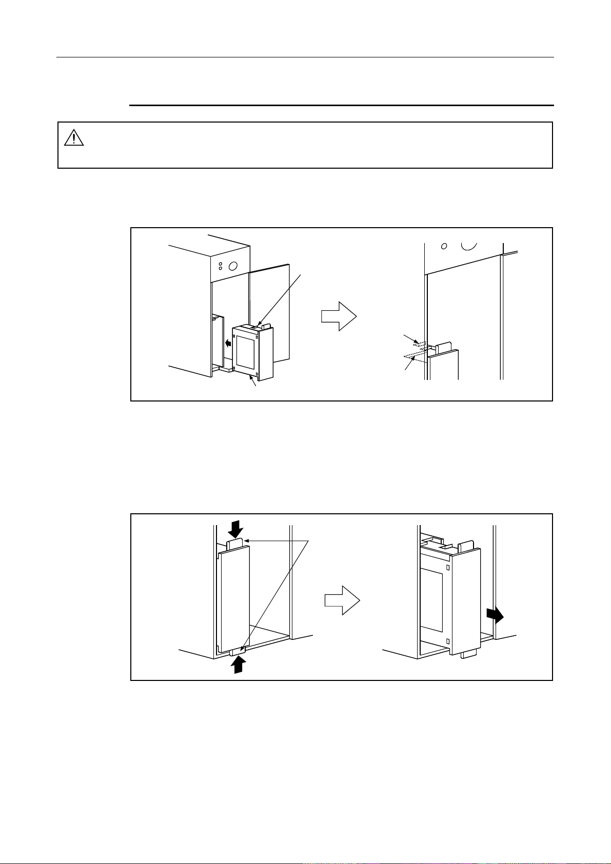
7. MEMORY CASSETTE AND BATTERY MELSEC-A
A
7.1.3 Installation and removal of memory cassette
•
CAUTION
How to install and remove the memory cassette is described below.
(1) Installation of the memory cassette
Make sure the memory cassette is installed securely in its installation connector. After
installation, confirm that it is securely tightened. Defective contact may cause
malfunctioning.
Hook
2USHCPU-S1
Hook
A2USHCPU-S1
Hook
Hook catch
A2SMCA
-14KP
(a) Position the side of the memory cassette with the model name facing the operator, then turn it
so that the model name is displayed on the top. Insert it into the memory cassette installation
port of the A2USHCPU-S1 until it makes a clicking sound (until the clip catches it).
(b) Confirm that the hooks provide on the top and bottom of the memory cassette are firmly
engaged with the hook catches. (If the memory cassette is not installed correctly, the front
cover of the A2USHCPU-S1 module does not close.)
(2) Removal of the memory cassette
Projections for hook
disengagement
A2USHCPU-S1
A2SMCA
-14KP
A2USHCPU-S1
A2SMCA
-14KP
(a) Pull the memory cassette while holding the projections for hook disengagement provided on
the top and bottom areas of the memory cassette by hand.
7-2
Page 78
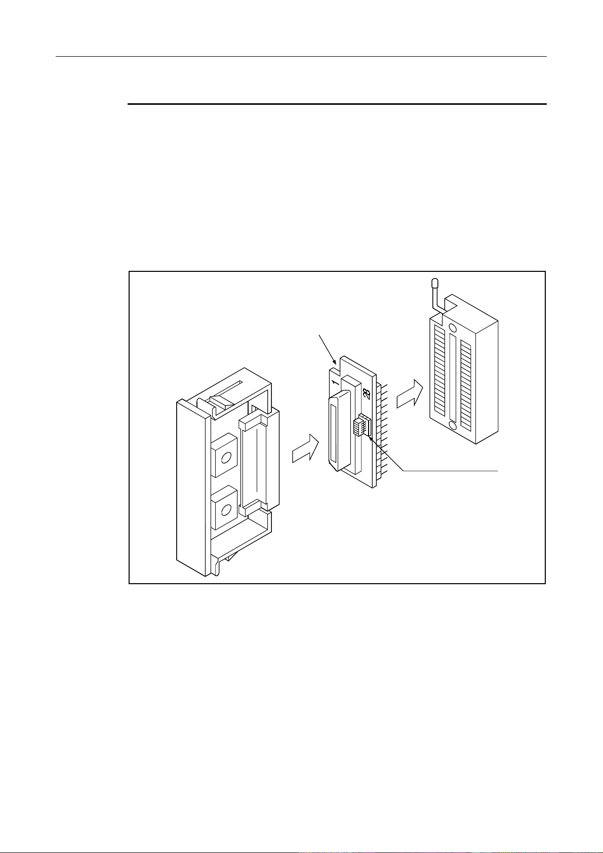
7. MEMORY CASSETTE AND BATTERY MELSEC-A
7.1.4 Procedure for writing sequence program t o A2SMCA-14KP
Writing a program to and erasing from A2SMCA-14KP can be accomplished by a ROM
writer/eraser.
If A2SMCA-14KP is installed to the ROM socket of A6GPP or A6WU, the memory write adapter
(A2SWA-28P) is necessary. How to use the A2SWA-28P is explained below.
(1) To write a program to the A2SMCA-14KP, it is necessary to divide it into odd-number
addresses and even-number addresses. Set the address type to write using the ODD/EVEN
selection pin of the A2SWA-28P.
(2) Connect the A2SMCA-14KP to the connector of A2SWA-28P. Be careful with the direction
of the connector.
(3) Connect the A2SWA-28P to which A2SMCA-14KP is connected to a ROM socket of A6GPP
or A6WU. At this juncture, pay attention not to mistake the connecting position. The pin near
the notched corner of the A2SWA-28P is the pin No.1.
Notch
ROM socket
ODD/EVEN selection pin
A2SWA-28P
A2SMCA-14KP
7-3
Page 79
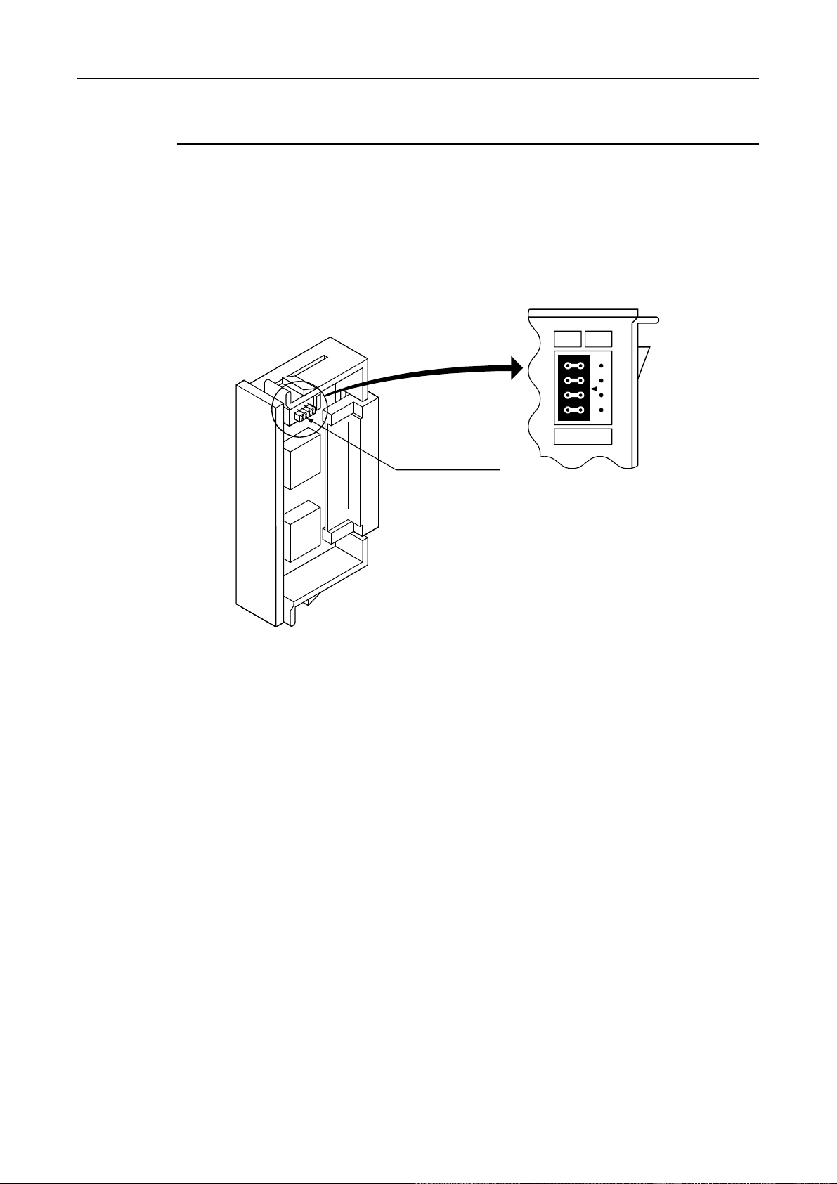
7. MEMORY CASSETTE AND BATTERY MELSEC-A
7.1.5 Memory protection setting of A2SNMCA-30KE
When A2USHCPU-S1 with A2SNMCA-30KE installed is used, it is necessary to setup the
memory protection on the body of A2SNMCA-30KE to prevent overwriting E
2
PROM memory
contents due to misoperation from a peripheral device.
64k bytes of the user memory area is protected as a whole by setting the memory protection
setting pin to ON.
To correct the ROM memory contents, cancel the memory protect (OFF).
At the time of factory shipment, memory protection setting pin is set to OFF.
For memory area allocation, refer to Section 4.2.2.
ON
OFF
Jumper
Memory protection
setting pin
M.PRO
Shows the memory
protection canceled state.
A2SNMCA-30KE
7-4
Page 80

7. MEMORY CASSETTE AND BATTERY MELSEC-A
7.2 Battery
Specification, precaution when handling and the installation procedure or the battery are described
below.
7.2.1 Specifications
Specifications of the battery used for the power failure retention function are shown in Table 7.2.
Table 7.2 Battery specifications
Model
Item
Nominal voltage 3.6VDC
Battery warranty period 5 years
Application For IC-RAM memory back up and power failure retention function
External dimensions (mm (inch))
7.2.2 Precautions when handling
Precautions when handling the battery are provided below.
(1) Do not short it.
(2) Do not disassemble it.
(3) Do not put it in a fire.
(4) Do not heat it.
(5) Do not solder to the electrodes.
7.2.3 Battery installation
A6BAT
16 (0.63) × 30 (1.18)
φ
Battery connector is removed to prevent consumption of the battery during shipping and storage.
Connect the lead connector of the battery to the battery connector on the A2USHCPU-S1 print
board before using A2USHCPU-S1 for the following objectives:
•
To use the sequence program in the user program area in the A2USHCPU-S1.
•
To use the power failure retention function.
A2USHCPU-S1
Battery
connector
A6BAT
7-5
Page 81

8. LOADING AND INSTALLATION MELSEC-A
8. LOADING AND INSTALLATION
To increase the system reliability and fully utilize the functions, procedures and cautions concerning
loading and installation are described below.
8.1 Concept of Failsafe Circuit
When turning the power supply of the PC ON or OFF, because of the delay and the difference in the
startup time between the power supply in the PC main module and the external power supply for
processing (especially DC), processing output may not operate normally for a moment.
For instance, when the PC power supply is turned on after a DC output module is turned on with the
external power supply for processing, the DC output module may misoutput momentarily upon PC
power-on. Therefore, it is necessary to construct a circuit whereby the power supply of the PC main
module can be energized first.
In addition, it may cause an abnormal operation when there is an abnormality in the external power
supply or a failure with the PC.
To prevent these abnormalities from causing abnormal behaviors of the system as a whole, and from
the stand point of failsafe, the circuits which may cause mechanical failures or accidents (the
emergency stop circuit, protection circuit, interlock circuits, etc.) should be constructed outside the PC.
An example of system circuit design in accordance with the view point mentioned above is shown on
the next page.
DANGER
•
Provide safety circuits in the outside of the PLC to ensure that the whole system
will operate safely if an external power supply fault or PLC failure occurs.
Not doing so may cause accidents due to improper output or malfunction.
(1) Configure circuits, such as emergency stop circuits, protective circuits,
oppositely operating interlock circuits, e.g. forward rotation and reverse
rotation, and machine damage prevention interlock circuits, e.g. upper and
lower limits of positioning, in the outside of the PLC.
(2) If the PLC detects either of the following faulty states, it stops arithmetic
operation and turns off all outputs.
•
When the overcurrent or overvoltage protection device of the power supply module
operates.
•
When a fault is detected by the self-diagnostic function of the PLC CPU such as a
watchdog timer error.
At the occurrence of a fault in the I/O control section, etc. that cannot be detected by
the PLC CPU, all outputs may turn on. Configure failsafe circuits or provide
mechanisms in the outside of the PLC to ensure that the machine operation will be
performed safely at such times.
(3) Depending on the failures of the output module relays, transistors, etc., the
outputs may remain on or off. Provide external monitoring circuits for the
output signals that may lead to serious accidents.
•
If excessive current higher than the rating or caused by a load short circuit, etc.
keeps flowing in the output module for a long period of time, smoking or ignition
may occur. Therefore, provide external safety circuits such as fuses.
8-1
Page 82

8. LOADING AND INSTALLATION MELSEC-A
(1) Example of system circuit design
In case of AC/DCIn case of AC
Power supply
Startup switch
Stop switch
MC
RA2
Output module
Transformer
Fuse
Ym
Yn
M9006
M9039
XM
Program
RA1
CPU
Ym
Yn
Y1
M9084
MC
Input module
L
RA1
XM
Signal input for
DC power supply
establishment
Startup/stop circuit
Startup possible with
RA1 ON which is a
RUN output of the PC.
Alarm output
(lamp or buzzer)
Becomes ON with
RUN by M9039
Power supply
Startup switch
Stop switch
MC
Transformer
Fuse
M9006
M9039
XM
TM
TM
N0
M10
RA1
RA2
Transformer
Ym
Yn
TM
M9084
MC1 N0 M10
MC
Input module
Fuse
XM
DC current
(+)
( )
Fuse
RA2
TM setting shall be time
until the DC input signal
is established.
A voltage relay is
recommended.
Output module
MC
MC2
MC1
MC1
MC2
Y1
RA2
Power supply to output
devices becomes OFF
on STOP
Upon emergency stop,
Upon stopping by hitting
the limit
Interlock circuits
Interlocking circuits are
constructed outside for parts
which may lead to conflicting
operations, such as forward
and reverse rotations,
mechanical failure and
accidents.
Startup procedure of power supply is as follows:
In case of AC
[1] Set CPU module to "RUN."
[2] Turn the power "ON."
[3] Set the start switch to "ON."
[4] Set the m agnet ic c ont ac t or (M C) "ON" to start driving drive
output devices by a program.
Output module
Ym
Yn
Output module
MC2
MC1
L
RA1
MC1
MC2
Alarm output
(lamp or buzzer)
Becomes ON with
RUN by M9039
MCMC
Power supply to
output devices
becomes OFF
on STOP
Upon emergency
stop, Upon stopping
by hitting the limit
In case of AC/DC
[1] Set CPU module to "RUN."
[2] Turn the power "ON."
[3] Set RA2 to "ON" when DC power supply is established.
[4] Set the timer (TM) to "ON" upon 100% establishment of DC power
supply.
(Set value for TM shall be the period from RA2 turned "ON" to 100%
establishment of DC power supply. Use the set value of 0.5s. )
[5] Set the start switch to "ON."
[6] Set the magnetic contactor (MC) "ON" to start driving drive output
devices by a program.
(When a voltage relay is used f or RA2, t he t im er in t he program (TM)
is not necessary.)
8-2
Page 83

8. LOADING AND INSTALLATION MELSEC-A
(2) Failsafe measures against PC failure
Failures in the PC CPU and memory are detected by the self-diagnostic function, but the CPU
may not be able to detect abnormalities in the I/O control area, etc.
In such cases, there is a possibility of setting all points to ON or OFF, or a situation may develop
where normal operations and safety of the controlled subject cannot be assured, depending on
the condition of the failure.
Although as a manufacturer, every possible measure is implemented to assure the product
quality, the failsafe circuit should be constructed outside by the user so that if the PC fails for
some reason, it would not cause any mechanical damages or accidents.
An example of failsafe circuit is shown below.
On-delay timer
Y00
Internal program
M9032
Y00
0.5s
0.5s
CPU module Output module
Y00
Y01
to
Y0F
24V
0V
External load
L
to
L
*1
T1
Off-delay timer
T2
– +
T2T1
1s
*2
1s
MC
24VDC
MC
*1 Since Y00 repeats ON/OFF with 0.5s intervals, use a contactless output module (transistor is
used in the above example).
*2 If an offdelay timer (especially miniature timer) is not available, construct the failsafe circuit
using an ondelay timer shown on the next page.
8-3
Page 84

8. LOADING AND INSTALLATION MELSEC-A
When constructing a failsafe circuit using ondelay timers only
On-delay timer
Y00
Internal program
M9032
0.5s 0.5s
Y00
Y00
Y01
to
Y0F
24V
0V
M1
M1
M2
T2
External load
to
– +
On-delay timer
L
L
24VDC
T1
1s
*1
M1
T2
1s
M2
MC
CPU module Output module
*1 Use a solid state relay for the M1 relay.
T1
M2
MC
8-4
Page 85

8. LOADING AND INSTALLATION MELSEC-A
8.2 Installation Environment
Avoid the following conditions for the installation location of A2USHCPU-S1 system:
(1) Location where the ambient temperature exceeds the range of 0 to 55°C.
(2) Location where the ambient humidity exceeds the range of 10 to 90%RH.
(3) Location where condensation occurs due to a sudden temperature change.
(4) Location where corrosive gas or flammable gas exists.
(5) Location where a lot of conductive powdery substance such as dust and iron filing, oil mist, salt, or
organic solvent exists.
(6) Location exposed to direct sunlight.
(7) Location where strong electric fields or magnetic fields form.
(8) Location where vibration or impact is directly applied to the main module.
8.3 Calculation Method of Heat Amount Generated by the PC
It is necessary to keep the temperature of the panel which stores the PC to the operating ambient
temperature of the PC, which is 55°C, or below.
For radiation design of the panel, it is necessary to know the average power consumption (heat
generation) of the devices and machinery stored inside. In this section, a method to obtain the av erage
power consumption of the A2USHCPU-S1 system is explained. Calculate the temperature increase in
the panel from the power consumption.
Calculation method of average power consumption
The power consuming parts of the PC may be roughly classified into the blocks as shown below:
I
5V
AC
power
supply
Power
supply
module
External
24VDC
power
supply
CPU
module
I
24V
5VDC line
24VDC line
Output
module
Relay
transistor
Output current
(I
) V
OUT
drop
AC
DC
Output
current
(I
OUT
LOAD
)
Input
module
Input current
(I
) E
IN
AC E
DC
Input
current
(I
IN
Special
function
module
Current
)
AC
DC
(1) Power consumption by power supply module
The power conversion efficiency of the power supply module is about 70%, and 30% is consumed
as heat generated, thus, 3/7 of the output power is the power consumption. Therefore, the
calculation formula is:
Wpw= {(I
3
7
5V
× 5) + (I
24V
× 24)} (W)
I5V : Current consumption of 5VDC logic circuit of each module
24V
I
: Average current consumption of 24VDC power supply for internal consumption of the output
module
(Current consumption equivalent to the points simultaneously ON)
.............. Not applicable to a system where 24VDC is supplied externally and a power
module which does not have a 24VDC output is used.
(2) Total power consumption of each module at 5VDC logic part
Power of the 5VDC output circuit of the power supply module is the power consumption of each
module.
W
5V=I5V
× 5 (W)
8-5
Page 86

8. LOADING AND INSTALLATION MELSEC-A
(3) Total 24VDC average pow er consumption of the output module (power consumption
equivalent to the points simultaneously ON)
Average power of the 24VDC output circuit of the power supply module is the total power
consumption of each module.
24V=I24V
W
(4) Average power consumption of the output modules due to voltage drops at the output part
(power consumption equivalent to the points simultaneously ON)
OUT
W
OUT
I
Vdrop : Voltage drop of each output module (V)
(5) Average power consumption of the input modules at the input part (power consumption
equivalent to the points simultaneously ON)
IN
W
IN
I
: Input current (actual value in case of AC) (A)
E : Input voltage (voltage for actual usage) (V)
(6) Power consumption of the power supply part of the special function module is:
× 24 (W)
OUT
= I
× Vdrop × Output points × Simultaneous ON ratio (W)
: Output current (current actually used) (A)
= IIN × E × Input points × Simultaneous ON ratio (W)
s
W
= I5V × 5 × I
24V
× 24 + I
100V
× 100 (W)
The total of the power consumption calculated for each block as above is the power consumption
of the PC system as a whole.
24V
W= WPW + W5V + W
+ W
OUT
+ WIN + WS (W)
Calculate the amount of heat generation and temperature increase inside the panel from the total
power consumption (W).
Simplified calculation formula to obtain temperature increase inside panel is shown next:
W
T= [°C]
UA
W : Power consumption of the PC system as a whole (the value obtained above)
2
A : Inside surface area of the panel [m
]
U : When inside temperature of the panel is kept constant by a fan, etc. ...............6
When the air inside the panel is not circulated..................................................4
POINT
When the temperature increase inside the panel exceeds the specified range, it is recommended
to lower the temperature inside the panel by installing a heat exchanger to the panel.
If a conventional ventilation fan is used, it sucks dust along with the outside air, which may affect
the PC, so care must be taken.
8-6
Page 87

8. LOADING AND INSTALLATION MELSEC-A
8.4 Installation of Base Unit
Precautions concerning installation of the basic base unit and extension base unit are described next.
8.4.1 Precautions when installing PC
Precautions concerning the installation of PC to the panel, etc. are explained below.
(1) To improve the ventilation and to facilitate the exchange of the module, provide at least 30mm
(1.18in.) of distance between the top part of the module and any structure or part.
However, when A52B, A55B, A58B, A62B, A65B or A68B extension base module is used, provide
at least 80mm (3.15in.) of distance between the top of the module and any structural part.
(2) Do not install vertically or horizontally, because of concerns with ventilation.
(3) If there are any protrusions, dents or distortion on the installation surface of the base unit, an
excessive force is applied to the print board and causes problems, so, install to a flat surface.
(4) Avoid sharing the same panel with any source of vibration such as a large magnetic contactor or
no-fuse breaker, and install to a separate panel or away from such devices.
(5) Provide wiring ducts as necessary.
However, when the clearance of the top and bottom of the PC are smaller than those shown in
figure 8.1, pay attention to the following:
(a) When installing to the top of PC, to improve the ventilation, keep the height of the duct to
50mm (1.97in.) or below.
In addition, the distance from the top of the PC should be sufficient for tightening and
loosening works for the installation screws on the top of the module.
The module cannot be replaced if the screws on the top of the module cannot be loosened
or tightened.
(b) When installing to the bottom part of the PC, provide a sufficient space so that the
100/200VAC input line of the power module, input and output cables of I/O modules and
12/24VDC lines are not affected.
(6) If any device is installed in front of the PC (i.e. installed in the back of the door), position it to
secure at least 100mm (3.94in.) of distance to avoid the effects of noise emission and heat.
Also, keep at least 50mm (1.97in.) distance from the base unit to any device placed on right or left
or the module.
8-7
Page 88

8. LOADING AND INSTALLATION MELSEC-A
8.4.2 Installation
Installation location of the basic base unit and the extension base unit is shown below.
Duct
(maximum height:
50mm (1.97 inch))
Basic base Extension base
Figure 8.1 Parallel installation
Indicates the location of ceiling of
the panel, wiring duct or other part.
Basic base (A1S3 B)
Extension base (A1S5 B, A1S6 B)
Indicates the location of ceiling of
the panel, wiring duct or other part.
At least
30mm
(1.18 inch)
At least
30mm
(1.18 inch)
At least
30mm
(1.18 inch)
At least
30mm
(1.18 inch)
At least
30mm
(1.18 inch)
At least
30mm
(1.18 inch)
Basic base (A1S3 B)
Extension base (A5 B, A6 B)
At least
30mm
(1.18 inch)
At least
30mm
(1.18 inch)
At least
80mm
(3.15 inch)
At least
80mm
(3.15 inch)
Panel, etc.
PC
Contactor
relay, etc.
At least 100mm (3.94 inch)
Figure 8.3 Distance between the
front face of the PC and
other devices
Figure 8.2 Series installation
Figure 8.4 Vertical installation
(not allowed)
Figure 8.5 Horizontal installation
(not allowed)
8-8
Page 89

8. LOADING AND INSTALLATION MELSEC-A
8.5 Installation and Removal of the Modules
How to install and remove the power supply module, CPU module, I/O module and special function
module, etc. to/from the base unit are explained.
•
CAUTION
Install the module by firmly inserting the projection for fixing the module at the
bottom of the module to the fixing hole of the base unit, then tighten the module
fixed screw with the specified torque. If the module is not installed correctly or
the screws are loose, malfunctions, failures and fall out may result.
•
Tighten the screws with the specified torque.
If the screws are loose, it may cause short-circuit, malfunctions, or the module
may fall out.
If the screw is tightened too much, it may cause short-circuit, malfunctions or the
module may fall out due to damaged screws or the module.
•
Before beginning any installation or wiring work, make sure all phases of the
power supply have been obstructed from the outside. Failure to completely shut
off the power-supply phases may cause breakdowns or malfunctions.
Base unit
Module installation screw
Module
8-9
Page 90
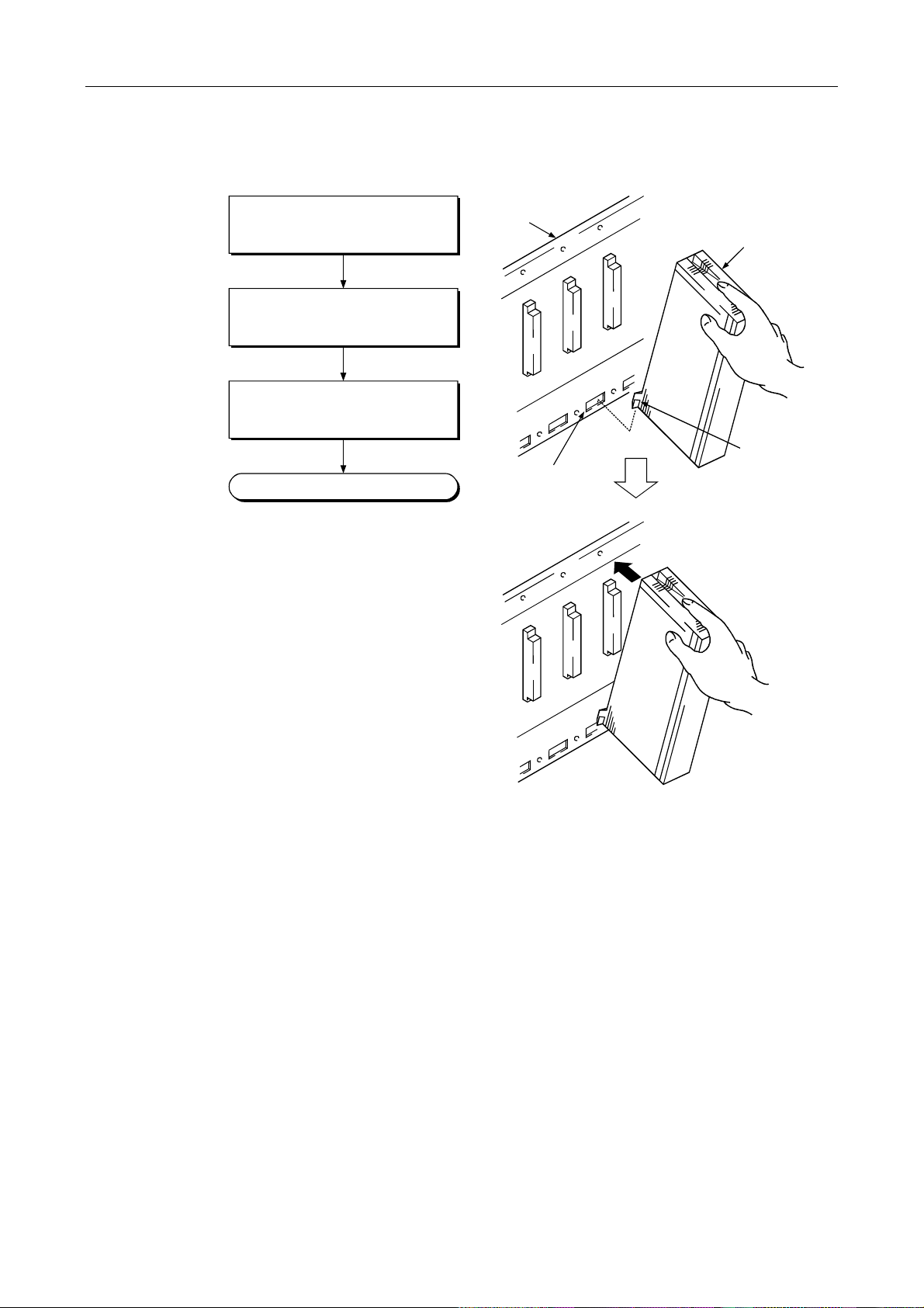
8. LOADING AND INSTALLATION MELSEC-A
(1) Installation of the module
Installation procedure of the module is explained.
Insert the module fixing projection
of the module into the module fixing
hole.
Install the module to the base unit
by pushing it in the direction of the
arrow.
Confirm that the module is firmly
inserted to the base unit, then
fix it with the module fixed scr ew.
Complete
Base unit
Module fixing hole
Module
Projection
for fixing
the module
8-10
Page 91

8. LOADING AND INSTALLATION MELSEC-A
(2) Removal of the module
Removal procedure of the module is explained.
Remove the module installation
screw, then pull out the top of the
module while using the bottom of
the module as the fulcrum.
Base unit
While lifting the module upward,
disengage the module fixing
projection from the module fixing
hole.
Complete
Module
connector
Module
Module fixing hole
POINT
To remove the module, the module installation screw must be removed first, then disengage the
projection for fixing the module from the module fixing hole. If the module is forcibly removed the
projection for fixing the module will be damaged.
8-11
Page 92

8. LOADING AND INSTALLATION MELSEC-A
p
8.6 Installation and Removal of the Dustproof Cover
When A1S52B, A1S55B or A1S58B is used, it is necessary to install the dustproof cover, which is
supplied with base to the I/O module to be installed to the left end in order to prevent intrusion of
foreign material into the I/O module. Intrusion of foreign materials into the I/O module may cause
breakdowns. Procedures for installing and removing the dustproof cover are described below.
(1) Installation
I/O module
To insert the dustproof cover to the I/O module, insert the cover to the connector or terminal side
first as shown in the figure, then push the cover to the I/O module side.
(2) Removal
Hole for removal
To remove the dustproof cover from the I/O module, insert the tip of a flat-tip screwdriver into the
removal hole as shown in the figure, then move the screwdriver towards the rear of the module to
separate the clip from the removal hole and remove the cover.
Dust-
roof cover
Dust-proof cover
I/O module
8-12
Page 93

8. LOADING AND INSTALLATION MELSEC-A
8.7 Wiring
8.7.1 Precautions when w iring
•
DANGER
CAUTION
Before beginning any installation or wiring work, make sure all phases of the
power supply have been obstructed from the outside. Failure to completely shut
off the power-supply phases may cause electric shock and/or damage to the
module.
•
When turning on the power or operating the module after installation or wiring
work, be sure the module's terminal covers are correctly attached. Failure to
attach the terminal covers may result in electric shock.
•
The FG and LG terminals should always be grounded using the class-3 or
higher grounding designed specially for PC. Failure to ground these terminals
may cause electric shock or malfunctioning.
•
When wiring the PC, check the rated voltage and terminal layout of the wiring,
and make sure the wiring is done correctly. Connecting a power supply that
differs from the rated voltage or wiring it incorrectly may cause fire or
breakdown.
•
Do not connect output from multiple power supply modules in parallel.
This may heat up the power supply module and cause fire or breakdowns.
•
Tighten the terminal screws with the specified torque. If the terminal screws are
loose, it may result in short circuits, fire or malfunctioning.
If the terminal screws are tightened too much, it may damage the screws and
the module may result in short circuits, malfunctioning or cause the module to
fall out.
•
Be careful not to let foreign matter such as filings or wire chips get inside the
unit. These can cause fire, breakdowns and malfunctioning.
•
Perform correct pressure-welding, crimp-contact or soldering for connectors for
the outside using the specified tools. Refer to the User's Manual of the
corresponding I/O module for tools required to perform pressure-welding and
crimp-contact.
Incorrect connection may cause short circuits, fire, or malfunctioning.
•
Do not bunch the control wires or communication cables with the main circuit or
power wires, or install them close to each other. They should be installed 100
mm (3.94in.) or more from each other. Failure to do so may result in noise that
would cause malfunctioning.
8-13
Page 94

8. LOADING AND INSTALLATION MELSEC-A
Precautions when wiring power supply cable are described.
(1) Wiring power supply
(a) Separate the PC's power supply line from the lines for I/O devices and power devices as
shown below.
When there is much noise, connect an insulation transformer.
200VAC
Main power
supply
PC power
supply
I/O power supply
Main circuit device
(b) 100VAC, 200VAC and 24VDC wires should be twisted as dense as possible. Connect the
modules with a shortest distance.
Also, to reduce the voltage drop to the minimum, use thickest wires possible (maximum
2
2mm
(0.0031in.2)).
Insulation
transformer
T1
PC
I/O devices
Main circuit device
(c) As a countermeasure to power surge due to lightening, connect a surge absorber for
lightening as shown below.
AC
E1
PC I/O
devices
E2
Surge absorber for lightening
POINT
(1) Separate the ground of the surge absorber for lightening (E1) from that of the PC (E2).
(2) Select a surge absorber for lightening whose power supply voltage does not exceed the
maximum allowable circuit voltage even at the time of maximum power supply voltage
elevation.
8-14
Page 95

8. LOADING AND INSTALLATION MELSEC-A
(2) Wiring I/O devices
(a) The suitable wire size for the connection to the terminals on a terminal block is 0.75 to
1.25mm
is recommended.
(b) Route the input wires separate from the output wires.
(c) When it is impossible to separate the input/output wires from the main circuit wires and the
power line, use a batch-shield cable and ground them at the PC side.
However, grounding them on the other side may be necessary in some cases.
2
(0.0012 to 0.0019in.2), but in view of ease of use, the wiring with wire size 0.75mm2
PC
Input
Shield cable
Output
Shield sheath
DC
RA
(d) When duct wiring is performed, ground the duct securely.
(e) Separate the 24VDC input and output lines from the 100VAC and 200VAC lines.
(f) With a long distance wiring of 200m (656.2ft.) or longer, leak current due to line capacity may
cause troubles. Implement the countermeasures described in Section 10.4.
(3) Grounding
Perform grounding according to (a) to (c) below.
(a) Employ independent grounding whenever possible. Grounding work shall be done with class
D (class 3) grounding. (Grounding resistance is 100Ω or less.)
(b) When independent grounding is not feasible, use shared grounding, shown as (2) in the
figure below.
PC
Class 3
grounding
Other
device
PC
Class 3
grounding
Other
device
PC
Other
device
(1) Independent grounding ····· Good (2) Independent grounding ····· O.K. (3) Independent grounding ····· Not allowed
(c) Use electrical wires having a thickness of at least 2mm
2
(0.0031in.2) for grounding.
Grounding point shall be as close to the PC as possible. Make the length of the ground wire
short.
8-15
Page 96

8. LOADING AND INSTALLATION MELSEC-A
8.7.2 Wiring to the module terminals
Examples of wiring power supply line and ground line to the basic base and the extension base are
shown below.
Wiring example
Insulation transformer
DC
AC
Fuse
24VDC
24VDC
100/110VAC
AC
Connect to the 24VDC
terminal of the module
which requires 24VDC
in the I/O module.
Basic base unit (A1S38B)
A1S62PN
Extension base unit (A1S68B)
A1S62PN
CPU module
+24V
24G
FG
LG
INPUT
100 to 240VAC
I/O
Extension cable
FG
100/110VAC
Ground line
Ground
LG
INPUT
100 to 240VAC
POINT
(1) For 100/200VAC and 24VDC power supply line, use the thickest electrical wire possible
(maximum 2mm
the crimp-style terminals, use crimp-style terminals with an insulation sleeve in order to avoid
short-circuiting when screws are loosened.
(2) When LG and FG terminals are connected, it must be grounded. When it is not grounded
with LG and FG terminals connected, it will be susceptible to noises. Since the LG terminal
has a potential of half the input voltage, touching the terminal may result in an electrical
shock.
2
(0.0031in.2)). The lines must be twisted from the connecting terminals. For
8-16
Page 97

8. LOADING AND INSTALLATION MELSEC-A
8.8 Precautions When Unfailure Power System (UPS) is Connected
When Unfailure Power System (abbreviated as UPS hereafter) is connected to the CPU system, care
must be taken on the following matter:
Use an UPS of inverter power supply type at all time with 5% or less voltage distortion. Do not use a
UPS of commercial power supply type.
8-17
Page 98

9. EMC DIRECTIVE AND LOW-VOLTAGE INSTRUCTION MELSEC-A
9. EMC DIRECTIVE AND LOW-VOLTAGE
INSTRUCTION
9.1 Requirements for Compliance to EMC Directive (89/336/EEC)
The EMC Directive (89/336/EEC) will become mandatory within Europe from
January 1st 1996. The EMC directive in essence defines the amount of
electromagnetic output a product is allowed to produce and how susceptible that
product is to electromagnetic interference. Any manufacturer or importer of
electrical/electronic apparatus must before releasing or selling products within
Europe after that date have either a CE mark attached to their goods. Testing to
comply with the directive is done by use of agreed European standards which define
limits for radiated and mains conducted electromagnetic emissions from equipment,
levels of immunity to radiated emissions, ability for equipment to cope with transient
voltage surges and electro-static discharges.
When installed in the specified manner this unit will be compliant with the relevant
standards EN50081-2 and prEN50082-2 as applicable in the EMC directive. Failure
to comply with these instructions could lead to impaired EMC performance of the
equipment and as such Mitsubishi Electric Corporation can accept no liability for such
actions.
9.1.1 EMC standards
When the PLC is installed following the directions given in this manual its EMC
performance is compliant to the following standards and levels as required by the
EMC directive.
Specifications Test Item Test Description Standard Values
EN50081-2 : 1995
EN55011
IEC801-2
prEN50082-2 : 1991 IEC801-3
IEC801-4
EN61000-4-2
EN61000-4-4
EN50082-2 : 1995 ENV50140
ENV50204
ENV50141
EN55011
Radiated noise
Conduction noise
Static electricity immunity *2
Radiated electromagnetic field *2
First transient burst noise
Static electricity immunity *2
First transient burst noise
Radiated electromagnetic field AM
modulation *2
Radiated electromagnetic field
Pulse modulation *2
Conduction noise
Measure the electric wave
released by the product.
Measure the noise released
by the product to the power
line.
Immunity test by applying
static electricity to the
module enclosure.
Immunity test by radiating an
electric field to the product.
Immunity test by applying
burst noise to the power line
and signal cable.
Immunity test by applying
static electricity to the
module enclosure.
Immunity test by applying
burst noise to the power line
and signal cable., 2 k V
Immunity test by radiating an
electric field to the product.
Immunity test by radiating an
electric field to the product.
Immunity test by inducting
electromagnetic field to the
power line signal cable.
30 M-230 M Hz QP : 30 dBµ V/m (30 m measurement) *1
230 M-1000 M Hz QP : 37 dBµ V/m (30 m measurement)
150 K-500k Hz QP: 79 dB, Mean : 66 dB *1
500 K-30M Hz QP : 73 dB, Mean: 60 dB
4 k V contact discharge
8 k V air discharge
10 V/m, 27-500 M Hz
2 k V
4 k V contact discharge
8 k V air discharge
2 k V
10 V/m, 80-1000 M Hz, 80 % AM modulation@1 k Hz
10 V/m, 900 M Hz, 200 Hz pulse modulation, 50 %
duty
10 Vrms, 0.15-80 M Hz, 80 % modulation@1 k Hz
9-1
Page 99

9. EMC DIRECTIVE AND LOW-VOLTAGE INSTRUCTION
(*1) QP: Quasi-peak value, Mean : Average value
(*2) The PLC is an open type device (device installed to another device) and must
be installed in a conductive control box.
The tests for the corresponding items were performed while the PLC was
installed to inside the control box.
9.1.2 Installation inside the cont rol cabi net
Since the PLC is an open type device (device incorporated into another device), it
must be installed in the control cabinet. This has a good effect of not only for assuring
safety but also for shielding noise emitted from the PLC, by means of the control
cabinet.
(1) Control cabinet
(a) Use a conductive control cabinet.
(b) When attaching the control cabinet's top plate or base plate, mask
painting and weld so that good surface contact can be made between the
cabinet and plate.
MELSEC-A
(c) To ensure good electrical contact with the control cabinet, mask the paint
on the installation bolts of the inner plate in the control cabinet so that
contact between surfaces can be ensured over the widest possible area.
(d) Earth the control cabinet with a thick wire so that a low impedance
connection to ground can be ensured even at high frequencies. (22 mm
wire or thicker is recommended.)
(e) Holes made in the control cabinet must be 10 cm (3.94 in.) diameter or
less. If the holes are 10 cm (3.94 in.) or larger, radio frequency noise may
be emitted.
(2) Connection of power and earth wires
Earthing and power supply wires for the PLC system must be connected as
described below.
(a) Provide an earthing point near the power supply module. Earth the power
supply's LG and FG terminals (LG : Line Ground, FG : Frame Ground)
with the thickest and shortest wire possible. (The wire length must be 30
cm (11.18 in.) or shorter.) The LG and FG terminals function is to pass the
noise generated in the PLC system to the ground, so an impedance that is
as low as possible must be ensured. As the wires are used to relieve the
noise, the wire itself carries a large noise content and thus short wiring
means that the wire is prevented from acting as an antenna.
2
Note) A long conductor will become a highly efficient antenna at high frequency.
9-2
Page 100

9. EMC DIRECTIVE AND LOW-VOLTAGE INSTRUCTION
(b) The earth wire led from the earthing point must be twisted with the power
supply wires. By twisting with the earthing wire, noise flowing from the
power supply wires can be relieved to the earthing. However, if a filter is
installed on the power supply wires, the wires and the earthing wire may
not need to be twisted.
9.1.3 Cables
The cables led from the control cabinet contain a high frequency noise element and
outside the control panel these cables act as antennae and radiate noise. The cables
connected to input/output modules or special modules which leave the control panel
must always be shielded cables.
Mounting of a ferrite core on the cables is not required (excluding some models) but
if a ferrite core is mounted, the noise radiated through the cable can be suppressed
further.
Use of a shielded cable is also effective for increasing the noise immunity level. The
PLC system's input/output and special function module provide a noise immunity
level of equivalent to that stated in IEC801-4 : 2 k V when a shielded cable is used. If
a shielded cable is not used or if the shield earthing treatment is not suitable even
when used (See Section 9.1.2.4), the noise immunity level is less than 2 k V.
Note) prEN50082-2 specifies the noise resistance level based on the signal wire
application.
Signals involved in process control : 2 k V
Signals not involved in process control : 1 k V
MELSEC-A
The meaning of "involved in process control" is not defined in prEN50082-2.
However, when the purposes of the EMC Directive are considered, the signals that
could cause personal injury or risks in the facility if a malfunction occurs should be
defined as "signals involved in process control". Thus, it is assumed that a high noise
immunity level is required.
9-3
 Loading...