

Page 1
Page 2

Page 3
SAFETY PRECAUTIONS
(Be sure to read these instructions before use.)
Before using the product, read this and relevant manuals carefully and handle the product correctly with full
attention to safety.
In this manual, SAFETY PRECAUTIONS are classified into 2 levels: "DANGER" and "CAUTION".
DANGER
CAUTION
Under some circumstances, failure to observe the CAUTION level instructions may also lead to serious
results.
Be sure to observe the instructions of both levels to ensure the safety.
Please keep this manual in a safe place for future reference and also pass this manual on to the end user.
Indicates that incorrect handling may cause hazardous conditions, resulting in
death or severe injury.
Indicates that incorrect handling may cause hazardous conditions, resulting in
medium or slight personal injury or physical damage.
[DESIGN PRECAUTIONS]
DANGER
Create a safety circuit outside the programmable controller to ensure the whole system will operate
safely even if an external power failure or a programmable controller failure occurs.
Otherwise, incorrect output or malfunction may cause an accident.
(1) For an emergency stop circuit, protection circuit and interlock circuit that is designed for
incompatible actions such as forward/reverse rotation or for damage prevention such as the
upper/lower limit setting in positioning, any of them must be created outside the programmable
controller.
Install the emergency stop switch outsid the controlpanel so that workers can operate it easily.
(2) When the programmable controller detects the following error conditions, it stops the operation
and turn off all the outputs.
• The overcurrent protection device or overvoltage protection device of the power supply
module is activated.
• The programmable controller CPU detects an error such as a watchdog timer error by the
self-diagnostics function.
In the case of an error of a part such as an I/O control part that cannot be detected by the
programmable controller CPU, all the outputs may turn on.In order to make all machines
operate safely in such a case, set up a fail-safe circuit or a specific mechanism outside the
programmable controller. For a fail-safe circuit example, refer to "LOADING AND
INSTALLATION" in this manual.
(3) Depending on the failure of the output module's relay or transistor, the output status may remain
ON or OFF incorrectly.
For output signals that may lead to a serious accident, create an external monitoring circuit.
A - 1
Page 4
[DESIGN PRECAUTIONS]
DANGER
If load current more than the rating or overcurrent due to a short circuit in the load has flowed in the
output module for a long time, it may cause a fire and smoke.
as a fuse.
Design a circuit so that the external power will be supplied after power-up of the programmable
controller.
Activating the external power supply prior to the programmable controller may result in an accident
due to incorrect output or malfunction.
For the operation status of each station at a communication error in data link, refer to the respective
data link manual.
The communication error may result in an accident due to incorrect output or malfunction.
When controlling a running programmable controller (data modification) by connecting a peripheral
device to the CPU module or a PC to a special function module, create an interlock circuit on
sequence programs so that the whole system functions safely all the time.
Also, before performing any other controls (e.g. program modification, operating status change
(status control)), read the manual carefully and ensure the safety.
In these controls, especially the one from an external device to a programmable controller in a
remote location, some programmable controller side problem may not be resolved immediately due
to failure of data communications.
To prevent this, create an interlock circuit on sequence programs and establish corrective
procedures for communication failure between the external device and the programmable controller
CPU.
Provide an external safety device such
When setting up the system, do not allow any empty slot on the base unit.
If any slot is left empty, be sure to use a blank cover (A1SG60) or a dummy module (A1SG62) for it.
When using the extension base unit, A1S52B(S1), A1S55B(S1) or A1S58B(S1), attach the included
dustproof cover to the module in slot 0.
Otherwise, internal parts of the module may be flied in the short circuit test or when an overcurrent or
overvoltage is accidentally applied to the external I/O section.
[DESIGN PRECAUTIONS]
CAUTION
Do not install the control lines or communication cables together with the main circuit or power lines,
or bring them close to each other.
Keep a distance of 100mm (3.94inch) or more between them.
Failure to do so may cause malfunctions due to noise.
When an output module is used to control the lamp load, heater, solenoid valve, etc., a large current
(ten times larger than the normal one) may flow at the time that the output status changes from OFF
to ON. Take some preventive measures such as replacing the output module with the one of a
suitable current rating.
A - 2
Page 5

[INSTALLATION PRECAUTIONS]
CAUTION
Use the programmable controller under the environment specified in the user's manual.
Otherwise, it may cause electric shocks, fires, malfunctions, product deterioration or damage.
Insert the module fixing projection into the fixing hole in the base unit and then tighten the module
fixing screw within the specified torque.
When no screw is tightened, even if the module is installed correctly, it may cause malfunctions, a
failure or a drop of the module.
Tightening the screw excessively may damage the screw and/or the module, resulting in a drop of
the module, a short circuit or malfunctions.
Connect the extension cable to the connector of the base unit or module.
Check for incomplete connection after installing it.
Poor electrical contact may cause incorrect inputs and/or outputs.
Insert the memory cassette and fully press it to the memory cassette connector.
Check for incomplete connection after installing it.
Poor electrical contact may cause malfunctions.
Be sure to shut off all phases of the external power supply used by the system before mounting or
removing the module.
Failure to do so may damage the module.
Do not directly touch the conductive part or electronic components of the module.
Doing so may cause malfunctions or a failure of the module.
A - 3
Page 6
[WIRING PRECAUTIONS]
DANGER
Be sure to shut off all phases of the external power supply used by the system before wiring.
Failure to do so may result in an electric shock or damage of the product.
Before energizing and operating the system after wiring, be sure to attach the terminal cover
supplied with the product.
Failure to do so may cause an electric shock.
CAUTION
Ground the FG and LG terminals correctly.
Failure to do so may cause an electric shock or malfunctions.
Wire the module correctly after confirming the rated voltage and terminal layout.
Connecting a power supply of a different voltage rating or incorrect wiring may cause a fire or failure.
Do not connect multiple power supply modules to one module in parallel.
The power supply modules may be heated, resulting in a fire or failure.
Press, crimp or properly solder the connector for external connection with the specified tool.
Incomplete connection may cause a short circuit, fire or malfunctions.
Tighten terminal screws within the specified torque range.
If the screw is too loose, it may cause a short circuit, fire or malfunctions.
Tightening the screw excessively may damage the screw and/or the module, resulting in a drop of
the module, a short circuit or malfunctions.
Carefully prevent foreign matter such as dust or wire chips from entering the module.
Failure to do so may cause a fire, failure or malfunctions.
Install our programmable controller in a control panel for use.
Wire the main power supply to the power supply module installed in a control panel through a
distribution terminal block.
Furthermore, the wiring and replacement of a power supply module have to be performed by a
maintenance worker who acquainted with shock protection.
(For the wiring methods, refer to Section 8.7.)
A - 4
Page 7
[STARTUP AND MAINTENANCE PRECAUTIONS]
DANGER
Do not touch any terminal during power distribution.
Doing so may cause an electric shock.
Properly connect batteries.
Do not charge, disassemble, heat or throw them into the fire and do not make them short-circuited
and soldered.
Incorrect battery handling may cause personal injuries or a fire due to exothermic heat, burst and/or
ignition.
Be sure to shut off all phases of the external power supply used by the system before cleaning or
retightening the terminal screws or module mounting screws.
Failure to do so may result in an electric shock.
If they are too loose, it may cause a short circuit or malfunctions.
Tightening the screw excessively may damage the screw and/or the module, resulting in a drop of
the module, a short circuit or malfunctions.
A - 5
Page 8

CAUTION
When performing online operations (especially, program modification, forced output or operating
status change) by connecting a peripheral device to the running CPU module, read the manual
carefully and ensure the safety.
Incorrect operation will cause mechanical damage or accidents.
Do not disassemble or modify each of modules.
Doing so may cause failure, malfunctions, personal injuries and/or a fire.
When using a wireless communication device such as a mobile phone, keep a distance of 25cm
(9.84inch) or more from the programmable controller in all directions.
Failure to do so may cause malfunctions.
Be sure to shut off all phases of the external power supply used by the system before mounting or
removing the module.
Failure to do so may result in failure or malfunctions of the module.
Do not drop or apply any impact to the battery.
Doing so may damage the battery, resulting in electrolyte spillage inside the battery.
If any impact has been applied, discard the battery and never use it.
Do not mount/remove the module onto/from base unit more than 50 times (IEC61131-2-compliant),
after the first use of the product.
Before handling modules, touch a grounded metal object to discharge the static electricity from the
human body.
Failure to do so may cause failure or malfunctions of the module.
A - 6
Page 9
[DISPOSAL PRECAUTIONS]
CAUTION
When disposing of the product, treat it as an industrial waste.
When disposing of batteries, separate them from other wastes according to the local regulations.
(For details of the battery directive in EU member states, refer to Appendix 6.)
[TRANSPORTATION PRECAUTIONS]
CAUTION
When transporting lithium batteries, make sure to treat them based on the transportation regulations.
(Refer to Appendix 5 for details of the relevant models.)
A - 7
Page 10
Revision
*The manual number is given on the bottom left of the back cover.
Print Date *Manual Number Revision
May., 1997 IB(NA)66779-A First edition
Nov., 1997 IB(NA)66779-B
Apr., 1998 IB(NA)-66779-C
Aug., 1998 IB(NA)-66779-D
Nov., 1998 IB(NA)-66779-E
Dec., 2002 IB(NA)-66779-F Equivalent to the Japanese version F
Dec., 2003 IB(NA)-66779-G
Correction
Contents, Related manuals, Section 1.1, Section 2.1.1, 2.1.2, Section 2.2, 2.3,
Chapter 3, Section 4.1.6, Section 5.1, 5.2, Section 6.1.2, Section 8.7.1, 8.7.2,
Section 9.1.3, Section 11.3.1, Appendix 1, 1.1, Appendix 3.1, 3.2, Appendix 5.
Correction
SAFETY PRECAUTIONS, Contents, Section 1.1, Section 2.2, 2.3, Section 4.1,
4.1.7, 4.1.8, 4.1.9, 4.4.3, Section 6.1.3, Section 7.1.4, Section 8.7.1, Section
9.2.1, 9.2.2, Section 11.3.1, Appendix 1, 1.1, Appendix 3.1, 3.2, 3.3.3.
Correction
Section 2.2.1, 2.3, Section 4.1, Section 9.1.2.7, 9.1.2.9 Section 11.2.4, Appendix
2.2, 3.3.5
Addition of module
A1SJHCPU-S8
Correction
SAFETY PRECAUTIONS, Section 1.1, 1.2, Section 2.1.1, 2.1.2, 2.2.1, 2.2.2, 2.3,
Chapter 3, Section 4.1.1, 4.1.7, Section 5.1, 5.2, Section 6.1.3, Section 7.1.1,
Section 9.1.4, Chapter 10, Section 11.1.3, Appendix 2.1, 2.2, Appendix 4
Addition of module
A1SY42P
Oct., 2006 IB(NA)-66779-H
Correction
Section 2.2.1, 2.3, Section 7.1.1, 7.1.4, 7.2.1, Section 8.4.1, 8.8, Section 9.1.4,
Section 11.3.1, Appendix 2.1
Addition
Appendix 5
Correction
SAFETY PRECAUTIONS, Section 2.2.1, 2.3, Chapter 3, Section 4.1, 4.1.2, 4.1.3,
4.1.4, 4.1.7, 4.2, 4.3, 4.4.1, 4.4.3, 4.4.4, Section 5.1, 5.2, Section 6.1.2, 6.1.3, 6.2,
Section 7.1.1, 7.1.3, Section 8.1, 8.3, 8.4.1, 8.4.2, 8.5, 8.7.1, 8.7.2, 8.8, Chapter
9, Section 9.1.3, 9.2.6, Chapter 10, Section 10.2, 10.3.2, Section 11.2.8, 11.3.2,
11.4.1, 11.4.2, Appendix 2.1, 2.2, Appendix 4.5.1, WARRANTY
Addition
USER PRECAUTONS, Section 7.2.2, Section 11.2.9, 11.3.1
A - 8
Page 11
Print Date *Manual Number Revision
May, 2007 IB(NA)-66779-I
Jul., 2007 IB(NA)-66779-J
Sep., 2008 IB(NA)-66779-K
Correction
Section 2.3, 8.7.1, 8.7.2, 9.1.3, 9.2.7, 10.3.1, 11.4.2
Addition
Section 9.1.7
Correction
Section 6.2, Appendix 4.4.1, Appendix 4.4.3, Appendix 4.4.4, Appendix 4.4.5,
Appendix 4.4.8, Appendix 4.4.9, Appendix 4.4.10
Correction
SAFETY PRECAUTIONS, Chapter 1, Section 2.2.2, 2.3, 2.4, Chapter 3,
Section 4.1, 4.1.1, 4.1.2, 4.1.3, 4.1.4, 4.1.5, 4.3, 4.4, 5.1, 8.1, 8.2, 8.3, 8.4.1,
8.4.2, 8.7.1, 8.7.2, 8.8, 9.1, 9.1.1, 9.1.2, 9.1.3, 9.2, 9.2.1, 9.2.2, 9.2.3, 9.2.4, 9.2.5,
9.2.6, 9.2.7, Chapter 10, Section 10.3.1, 10.3.2, 11.1, 11.2.3, 11.3, 11.4.1, 11.2.8,
Appendix 1, Appendix2.2
Addition
Appendix 6, Appendix 6.1, Appendix 6.2
Japanese Manual Version SH-3635-L
This manual confers no industrial property rights or any rights of any other kind, nor dose it confer any patent
licenses.Mitsubishi Electric Corporation cannot be held responsible for any problems involving industrial property rights
which may occur as a result of using the contents noted in this manual.
1997 MITSUBISHI ELECTRIC CORPORATION
A - 9
Page 12

Introduction
Thank you for purchasing the Mitsubishi programmable logic controller MELSEC-A Series.
Prior to use, please read this manual thoroughly to fully understand the functions.
Please hand in a copy of this manual to the end user.
Table of Contents
1 OVERVIEW 1 - 1 to 1 - 4
1.1 Features ........................................................................................................................................1 - 2
2 SYSTEM CONFIGURATION 2 - 1 to 2 - 30
2.1 Overall Configuration.....................................................................................................................2 - 1
2.1.1 Overall configuration of AnSHCPU .......................................................................................2 - 1
2.1.2 Overall configuration of A1SJHCPU(S8)...............................................................................2 - 3
2.2 Precautions when Configuring the System ...................................................................................2 - 5
2.2.1 Hardware...............................................................................................................................2 - 5
2.2.2 Software package .................................................................................................................2 - 9
2.3 System Equipment ......................................................................................................................2 - 11
2.4 System Configuration Overview ..................................................................................................2 - 26
3 SPECIFICATIONS 3 - 1 to 3 - 1
4 CPU MODULE 4 - 1 to 4 - 29
4.1 Performance Specifications...........................................................................................................4 - 1
4.1.1 Overview of operation processing .........................................................................................4 - 4
4.1.2 Operation processing of RUN, STOP and PAUSE ...............................................................4 - 7
4.1.3 Operation processing upon instantaneous power failure ......................................................4 - 9
4.1.4 Self-diagnostics function .....................................................................................................4 - 10
4.1.5 Device list............................................................................................................................4 - 13
4.2 Parameter Setting Ranges ..........................................................................................................4 - 15
4.2.1 List of parameter setting range ...........................................................................................4 - 15
4.2.2 Memory capacity setting (for main program, file register, comment, etc.) ..........................4 - 17
4.3 Function List ................................................................................................................................4 - 19
4.4 Handling Precautions ..................................................................................................................4 - 21
4.5 Part Names .................................................................................................................................4 - 22
4.5.1 Parts names of the A1SHCPU, A2SHCPU(S1), A1SJHCPU (S8)......................................4 - 22
4.5.2 Setting of I/O control mode switching switch.......................................................................4 - 26
4.5.3 Settings for memory write protect switch ............................................................................4 - 27
4.5.4 Latch clear operation...........................................................................................................4 - 29
5 POWER SUPPLY MODULE 5 - 1 to 5 - 6
5.1 Specifications ................................................................................................................................5 - 1
5.1.1 Power supply module selection.............................................................................................5 - 4
5.2 Part Names ...................................................................................................................................5 - 5
A - 10
Page 13

6 BASE UNIT AND EXTENSION CABLE 6 - 1 to 6 - 10
6.1 Specifications ................................................................................................................................6 - 1
6.1.1 Base unit specifications.........................................................................................................6 - 1
6.1.2 Extension cable specifications ..............................................................................................6 - 2
6.1.3 Application standards of extension base units (A1S52B(S1), A1S55B(S1), A1S58B(S1), A52B,
A55B, A58B) .........................................................................................................................6 - 3
6.2 Part Names ...................................................................................................................................6 - 7
6.3 Installation and Removal of DIN Rail.............................................................................................6 - 9
7 MEMORY CASSETTE AND BATTERY 7 - 1 to 7 - 8
7.1 Memory Cassette ..........................................................................................................................7 - 1
7.1.1 Specifications ........................................................................................................................7 - 1
7.1.2 Handling precautions ............................................................................................................7 - 2
7.1.3 Installation and removal of memory cassette........................................................................7 - 3
7.1.4 Writing a sequence program to a memory cassette..............................................................7 - 5
7.1.5 Memory protection setting of A2SNMCA-30KE ....................................................................7 - 6
7.2 Battery ...........................................................................................................................................7 - 7
7.2.1 Specifications ........................................................................................................................7 - 7
7.2.2 Handling precautions ............................................................................................................7 - 7
7.2.3 Battery installation.................................................................................................................7 - 8
8 LOADING AND INSTALLATION 8 - 1 to 8 - 23
8.1 Fail-Safe Circuit Concept ..............................................................................................................8 - 1
8.2 Installation Environment ................................................................................................................8 - 6
8.3 Calculation Method of Heat Amount Generated by the PLC .........................................................8 - 7
8.4 Installing the Base Units................................................................................................................8 - 9
8.4.1 Precautions when installing programmable controller...........................................................8 - 9
8.4.2 Installation ...........................................................................................................................8 - 10
8.5 Installation and Removal of the Base Units.................................................................................8 - 11
8.6 Installation and Removal of the Dustproof Cover........................................................................8 - 14
8.7 Wiring ..........................................................................................................................................8 - 16
8.7.1 Wiring instructions...............................................................................................................8 - 16
8.7.2 Wiring to module terminals..................................................................................................8 - 21
8.8 Precautions when Connecting the Uninterruptible Power Supply (UPS) ....................................8 - 23
9 EMC AND LOW VOLTAGE DIRECTIVES 9 - 1 to 9 - 13
9.1 Requirements for Compliance with EMC Directives......................................................................9 - 1
9.1.1 EMC standards .....................................................................................................................9 - 1
9.1.2 Installation instructions for EMC directive .............................................................................9 - 2
9.1.3 Cables ...................................................................................................................................9 - 3
9.1.4 Power supply module............................................................................................................9 - 8
9.1.5 Ferrite core............................................................................................................................9 - 8
9.1.6 Noise filter (power supply line filter) ......................................................................................9 - 9
9.1.7 Power line for external power supply terminal ......................................................................9 - 9
9.2 Requirements for Compliance with Low Voltage Directives........................................................9 - 10
A - 11
Page 14

9.2.1 Standard applied for MELSEC-AnS series programmable controller .................................9 - 10
9.2.2 Precautions when using the MELSEC-AnS series programmable controller......................9 - 10
9.2.3 Power supply.......................................................................................................................9 - 11
9.2.4 Control panel.......................................................................................................................9 - 12
9.2.5 Module installation ..............................................................................................................9 - 13
9.2.6 Grounding ...........................................................................................................................9 - 13
9.2.7 External wiring.....................................................................................................................9 - 13
10 MAINTENANCE AND INSPECTION 10 - 1 to 10 - 8
10.1 Daily Inspection ...........................................................................................................................10 - 2
10.2 Periodic Inspection ......................................................................................................................10 - 3
10.3 Battery Replacement ...................................................................................................................10 - 4
10.3.1 Battery life ...........................................................................................................................10 - 4
10.3.2 Battery replacement procedure...........................................................................................10 - 8
11 TROUBLESHOOTING 11 - 1 to 11 - 22
11.1 Fundamentals of Troubleshooting ...............................................................................................11 - 1
11.2 Troubleshooting...........................................................................................................................11 - 2
11.2.1 Troubleshooting procedure .................................................................................................11 - 2
11.2.2 Flow for actions when the "POWER" LED is turned OFF ...................................................11 - 3
11.2.3 Flow for actions when the "RUN" LED is turned OFF .........................................................11 - 4
11.2.4 Flow for actions when the "RUN" LED is flickering .............................................................11 - 5
11.2.5 Flow for actions when the "ERROR" LED is turned ON......................................................11 - 6
11.2.6 Flow for actions when the "ERROR" LED is flickering ........................................................11 - 7
11.2.7 Flow for actions when the output module's output load does not turn ON ..........................11 - 8
11.2.8 Flow for actions when the program cannot be written.........................................................11 - 9
11.2.9 Flow for actions when the CPU module is not started up .................................................11 - 10
11.3 Error Code List ..........................................................................................................................11 - 11
11.3.1 Procedure to read an error code .......................................................................................11 - 11
11.3.2 AnSHCPU error code list ..................................................................................................11 - 12
11.4 Fault Examples with I/O Modules..............................................................................................11 - 17
11.4.1 Faults with the input circuit and the corrective actions ......................................................11 - 17
11.4.2 Faults in the output circuit .................................................................................................11 - 19
APPENDIX Appendix - 1 to Appendix - 57
Appendix 1 Instruction List .............................................................................................................. App - 1
Appendix 1.1 Precautions for write during RUN of a dedicated instruction .............................. App - 7
Appendix 2 LISTS OF SPECIAL RELAYS AND SPECIAL REGISTERS ...................................... App - 8
Appendix 2.1 List of Special Relays......................................................................................... App - 8
Appendix 2.2 Special Registers ............................................................................................. App - 20
Appendix 3 Precautions when Replacing AnSCPU with AnSHCPU ............................................. App - 39
Appendix 3.1 Differences between A1SHCPU and A1SCPU................................................. App - 39
Appendix 3.2 Differences between A2SHCPU(S1) and A2SCPU .......................................... App - 40
Appendix 3.3 Replacement precautions ................................................................................. App - 40
Appendix 3.3.1 PLC type setting ........................................................................................ App - 40
Appendix 3.3.2 Precautions when performing ROM partition ............................................. App - 40
A - 12
Page 15

Appendix 3.3.3 Precautions when utilizing sequence programs ........................................ App - 41
Appendix 3.3.4 Checking the influence of the increased instruction processing speed on the
system ....................................................................................................... App - 41
Appendix 3.3.5 Handling conventional memory cassettes ................................................. App - 42
Appendix 3.3.6 Replacing the A2SMCA-14KP (when A2SCPU + A2SMCA-14KP has been used)
................................................................................................................... App - 42
Appendix 3.3.7 Restrictions on microcomputer programs .................................................. App - 42
Appendix 4 External Dimensions .................................................................................................. App - 43
Appendix 4.1 CPU module...................................................................................................... App - 43
Appendix 4.1.1 A1SHCPU, A2SHCPU(S1) module ........................................................... App - 43
Appendix 4.1.2 A1SJHCPU module ................................................................................... App - 43
Appendix 4.1.3 A1SJHCPU-S8 module.............................................................................. App - 44
Appendix 4.2 A1S61PN, A1S62PN and A1S63P power supply modules .............................. App - 45
Appendix 4.3 Main base unit................................................................................................... App - 46
Appendix 4.3.1 A1S32B main base unit ............................................................................. App - 46
Appendix 4.3.2 A1S33B main base unit ............................................................................. App - 46
Appendix 4.3.3 A1S35B main base unit ............................................................................. App - 47
Appendix 4.3.4 A1S38B main base unit ............................................................................. App - 47
Appendix 4.4 Extension base unit........................................................................................... App - 48
Appendix 4.4.1 A1S65B extension base unit...................................................................... App - 48
Appendix 4.4.2 A1S68B extension base unit...................................................................... App - 48
Appendix 4.4.3 A1S52B extension base unit...................................................................... App - 49
Appendix 4.4.4 A1S55B extension base unit...................................................................... App - 49
Appendix 4.4.5 A1S58B extension base unit...................................................................... App - 50
Appendix 4.4.6 A1S65B-S1 extension base unit ................................................................ App - 50
Appendix 4.4.7 A1S68B-S1 extension base unit ................................................................ App - 51
Appendix 4.4.8 A1S52B-S1 extension base unit ................................................................ App - 51
Appendix 4.4.9 A1S55B-S1 extension base unit ................................................................ App - 52
Appendix 4.4.10 A1S58B-S1 extension base unit................................................................ App - 52
Appendix 4.5 Memory cassette............................................................................................... App - 53
Appendix 4.5.1 AnSNMCA-[ ] memory cassette ................................................................. App - 53
Appendix 4.6 Memory write adapter ....................................................................................... App - 53
Appendix 4.6.1 A6WA-28P memory write adapter ............................................................. App - 53
Appendix 5 Transportation Precautions ........................................................................................ App - 54
Appendix 5.1 Relevant models ............................................................................................... App - 54
Appendix 5.2 Transportation Guidelines................................................................................. App - 55
Appendix 6 Handling of Batteries and Devices with Built-in Batteries in EU Countries ................ App - 56
Appendix 6.1 Disposal precautions......................................................................................... App - 56
Appendix 6.2 Exportation precautions .................................................................................... App - 57
INDEX Index - 1 to Index - 3
A - 13
Page 16

About This Manual
Related manuals
The following manuals are related to this product.
Manual Name
ACPU/QCPU-A (A mode) Programming Manual (Fundamentals)
Describes programming methods necessary for creating programs, device names, parame-
ters, program types, memory area configuration, and so on. (Sold separately)
ACPU/QCPU-A (A mode) Programming Manual (Common Instructions)
Describes how to use the sequence instruction, basic instructions, applied instructions and
microcomputer programs. (Sold separately)
AnSHCPU/AnACPU/AnUCPU/QCPU-A (A Mode) Programming Manual (Dedicated Instructions)
Describes instructions that have been expanded for AnSHCPU
(Sold separately)
AnS Module type I/O User's Manual
Describes the specification of the compact building block type I/O module.
(Sold separately)
Manual No.
(Model Code)
IB-66249
(13J740)
IB-66250
(13J741)
IB-66251
(13J742)
IB-66541
(13JE81)
A - 14
Page 17

USER PRECAUTIONS
Precautions when using the AnS series
For a new CPU module, which has never used before, the contents of built-in RAM and
device data are undefined.
Make sure to clear the built-in RAM memory (PLC memory all clear) in the CPU module by
peripheral devices and operate latch clear by RUN/STOP key switches.
Precautions for battery
(1) The operation after a battery is unmounted and the programmable controller is stored.
When reoperating after a battery is uncounted and the programmable controller is
stored, the contents of built-in RAM and device data may be undefined.
For this reason, make sure to clear the built-in RAM memory (PLC memory all clear) in
the CPU module by peripheral devices and operate latch clear by RUN/STOP key
switches before start the operation again.
After the built-in RAM clear and latch clear of the CPU module, write the backed-up
memory contents to the CPU module before saving.
(2) The operation after excess of a battery life
If a battery exceeded its guaranteed life is stored and reoperated, the contents of built-in
RAM and device data may be undefined.
For this reason, make sure to clear the built-in RAM memory (PLC memory all clear) in
the CPU module by peripheral devices and operate latch clear by RUN/STOP key
switches before start the operation again.
After the built-in RAM clear and latch clear of the CPU module, write the backed-up
memory contents to the CPU module before saving.
*
*
POINT
Make sure to back up each memory contents before storing the programmable
controller.
* Refer to the following manuals for details of built-in RAM clear (PLC memory all clear) by periph-
eral devices.
GX Developer Operating Manual
A6GPP/A6PHP Operating Manual
SW IVD-GPPA Operating Manual
Refer to Section 4.5 for latch clear operation by RUN/STOP key switch of the CPU module.
A - 15
Page 18

1. OVERVIEW
1 OVERVIEW
This user's manual describes the functions, specification, and handling of the A1SJHCPU
general purpose programmable controller (abbreviated as A1SJHCPU from here on),
A1SJHCPU-S8 general purpose programmable controller (abbreviated as A1SJHCPUS8), A1SHCPU general purpose PLC (abbreviated as A1SHCPU), A2SHCPU general
purpose PLC (abbreviated as A2SHCPU), and A2SHCPU-S1 general purpose PLC
(abbreviated as A2SHCPU-S1).
A1SHCPU and A1SJHCPU are grouped as A1SHCPU, unless there is necessity to
identify each model.
Also, A1SHCPU, A2SHCPU and A2SHCPU-S1 are grouped as AnSHCPU, unless there
is necessity to identify each model.
The AnSHCPU is a compact-type building block programmable controller. The model is
one third the size of the conventional building block type programmable controller, and
allows easy operation in spite of its small size.
Sequence programs that have been created for the existing A0J2CPU, A0J2HCPU and
A NCPU models can be used by changing the CPU module type specification for the
program. Moreover, since modules for use with A NCPU can be used by installing them
on an extension base unit for A NCPU use, it is possible to extend the functions of an
AnSCPU.
This user's manual refers to peripheral devices by using the following abbreviations.
A6GPP, A6PHP, PC/AT (started up with SW IVD-GPPA)
......................................................... Abbreviated as "GPP function".
A7PUS, A8PUE .............................. Abbreviated as "PU".
1 - 1
Page 19

1. OVERVIEW
1.1 Features
(1) High-speed operation processing speed
Compared to the conventional A1SCPU, the A1SHCPU is three times and A2SHCPU
(S1) is four times faster in the operation processing speed, respectively.
Item A1SHCPU A2SHCPU(S1) A1SCPU
Operation processing speed
*1 I/O processing: Refresh and LD instruction
*1
0.33 s 0.25 s 1 s
(2) Addition of new dedicated instructions
The CC-Link dedicated instructions (8 instructions) have been added, making the
operation even easier.
(3) Increased number of I/O device points
The actual number of I/O points is the same as the AnS series, but each CPU has
2048 points (X/Y0 to X/Y7FF) of I/O devices.
The added I/O device can be used as the MELSECNET (/B), MELSECNET/MINI-S3,
or CC-Link.
(4) Increased file register R capacity
The capacity is now max. 8192 points (R0 to R8191), which doubled the AnS series'
4096 points (R0 to R4095).
(5) Increased memory capacity (Increased number of comment points)
The A1SHCPU has 64 k bytes, which doubled the A1SCPU's 32 k bytes.
This increased the number of comment points stored in the CPU module 3648 points
in comparison to the 1600 points in A1SCPU.
(6) Full compatibility with A1S(S1)/A2SCPU(S1)
Because there is full compatibility of the functions and instructions with A1S(S1)/
A2SCPU(S1), all software packages can be used.
In addition, power supply module, base unit, and I/O modules can be used.
(7) Compact size
The appearance of the AnSHCPU system with one power supply module, one CPU,
and eight 16-point I/O modules for use with AnS mounted to the main base unit are:
430mm (16.9in.) (W); 130mm (5.12in.) (H); and 110mm (4.33in.) (D).
(8) Max. 8 k/14 k steps of program
An A1SHCPU allows the creation of a sequence program up to 8k steps, an
A2SHCPU(S1) allows up to 14k steps.
In addition, microcomputer programs and utility programs created by the user can be
used.
1 - 2
Page 20

OVERVIEW1.
(9) SFC language compatible
An AnSCPU contains a microcomputer program area, so an SFC program can be
used.
(10) Two extension connectors, on the right and left sides. (A1SHCPU,A2SHCPU(S1))
In order to facilitate wiring wherever the extension base unit is installed, extension
connectors are provided at both left and right sides of the AnSHCPU and extension
cables that suit the requirements imposed by different mounting locations are
available.
* A1SJHCPU(S8) on the right side only
(11) Use either screws or DIN rail for panel installations
The AnS base unit is provided both with screw holes and, on its rear face, the fixture
for mounting it to a DIN rail.
(12) Easy-to-see terminal block symbol sheet
• A terminal block symbol sheet is attached to the front of AnS I/O modules.
AnSHCPU writes I/O device numbers, connector numbers, etc. on one side of the
sheet.
• Terminal symbols for 16 I/O signals can be written on the other side.
(13) A N, A A-series I/O module and special function module compatible
By connecting an A N, A A-series extension base unit, A N, A A I/O
modules or special function modules can be used.
(14) Same programming environment as other MELSEC-A CPU modules
A sequence program can be created using the peripheral device currently used for
other MELSEC-A CPU modules. For details on the applicable peripheral devices,
refer to Section 2.2 "Precautions when Configuring the System".
1 - 3
Page 21

OVERVIEW1.
MEMO
1 - 4
Page 22
2. SYSTEM CONFIGURATION
2 SYSTEM CONFIGURATION
This chapter describes the applicable system configurations, cautions on configuring a
system, and component devices of the AnSHCPU.
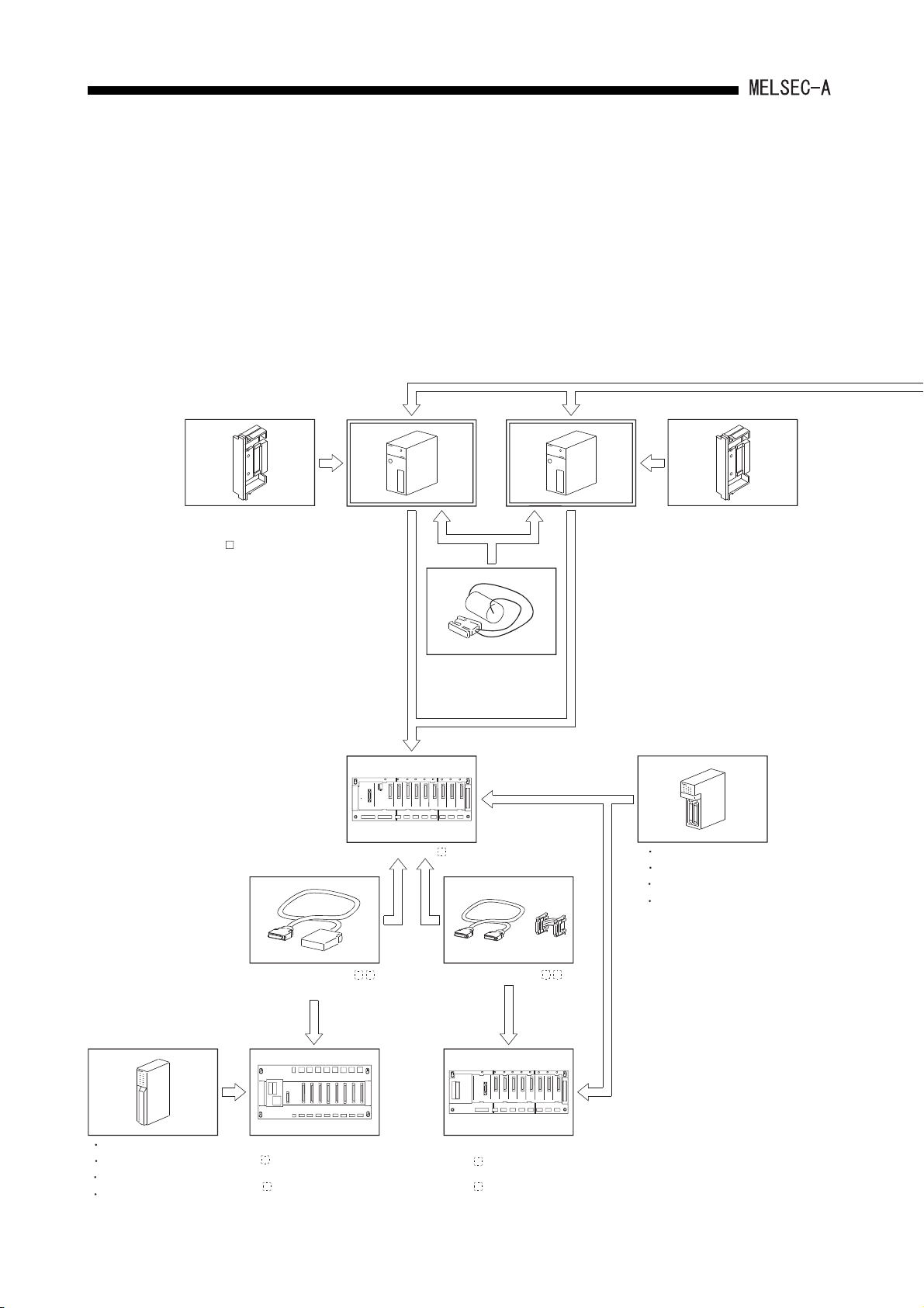
2.1 Overall Configuration
2.1.1 Overall configuration of AnSHCPU
The following figure shows configurations of an AnSHCPU stand-alone system and a
peripheral device.
(To peripheral devices)
ROM cassette
(A1SNMCA-8KP with EP-ROM)
(A1SNMCA- KE with E2PROM)
A1SHCPU
Main base(A1S3 B)
Battery (A6BAT)
A2SHCPU(S1)
ROM cassette
(A2SNMCA-30KE with E PROM)
Power supply module
Input module
Output module
Special function module
2
Power supply module
Input module
Output module
Special function module
Extension cable (A1SC0 NB)
[Building-block type]
Extension base
(A5 B)
: without a power supply module
(A6 B)
: with a power supply module
Extension cable (A1SC NB)
Extension base
(A1S5 B(S1))
: without a power supply module
(A1S6 B(S1))
: with a power supply module
2 - 1
Page 23
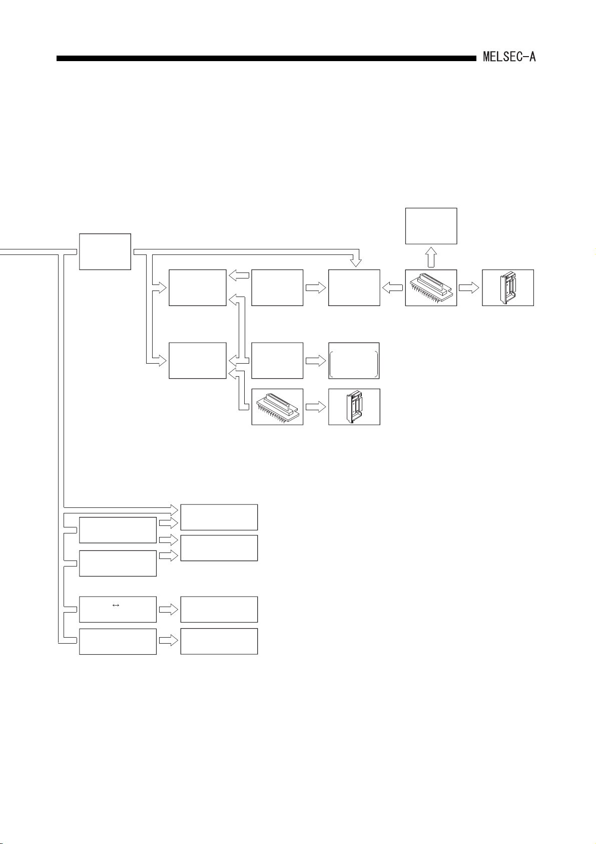
SYSTEM CONFIGURATION2.
To CPU module
AC30R4
AC300R4
cable
AC30R4-PUS
cable
AC20R4-A8PU
cable
A6PHP
Plasma hand-held
graphic programmer
A6GPP intelligent
GPP
A7PUS
programming unit
A8PUE
programming unit
AC03WU
cable
AC30R2
cable
EP-ROM write adapter
(A6WA-28P)
A6WU
P-ROM writer
module
Printer
A7NPR-S1,
K6PR-K,
Generalpurpose printer
ROM cassette
(A1SNMCA-8KP)
ROM writer
*
EP-ROM write adapter
(A6WA-28P)
ROM cassette
(A1SNMCA-8KP)
RS-232C RS-422
converter
AC30R4-PUS
cable
IBM-PC/AT-compatible
personal computer
A6DU-B
data access module
2 - 2
Page 24
SYSTEM CONFIGURATION2.
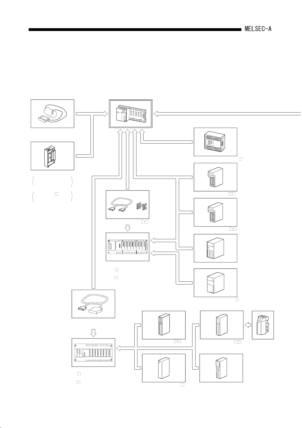
2.1.2 Overall configuration of A1SJHCPU(S8)
The following figure shows configurations of a A1SJHCPU(S8) stand-alone system and
peripheral device.
A1SJHCPU(S8)
Battery (A6BAT)
(To peripheral device)
Thin type I/O module (A1SJ-56 )
ROM cassette
A1SNMCA-8KP
with EP-ROM
A1SNMCA- KE
2
with E PROM
Extension cable (A1SC B)
Extension base
(A1S5 B(S1))
:Without a power supply module
(A1S6 B(S1))
:With a power supply module
Extension cable (A1SC05NB)
[Building block type]
Input module (A1SX )
Output module (A1SY )
Special function module
Power supply module (A1S6 P)
Extension base
(A5 B)
:Without a power supply module
(A6 B)
:With a power supply module
Input module (AX )
Power supply module (A6 P)
2 - 3
Output module (AY )
Special function module
Fuse
Page 25
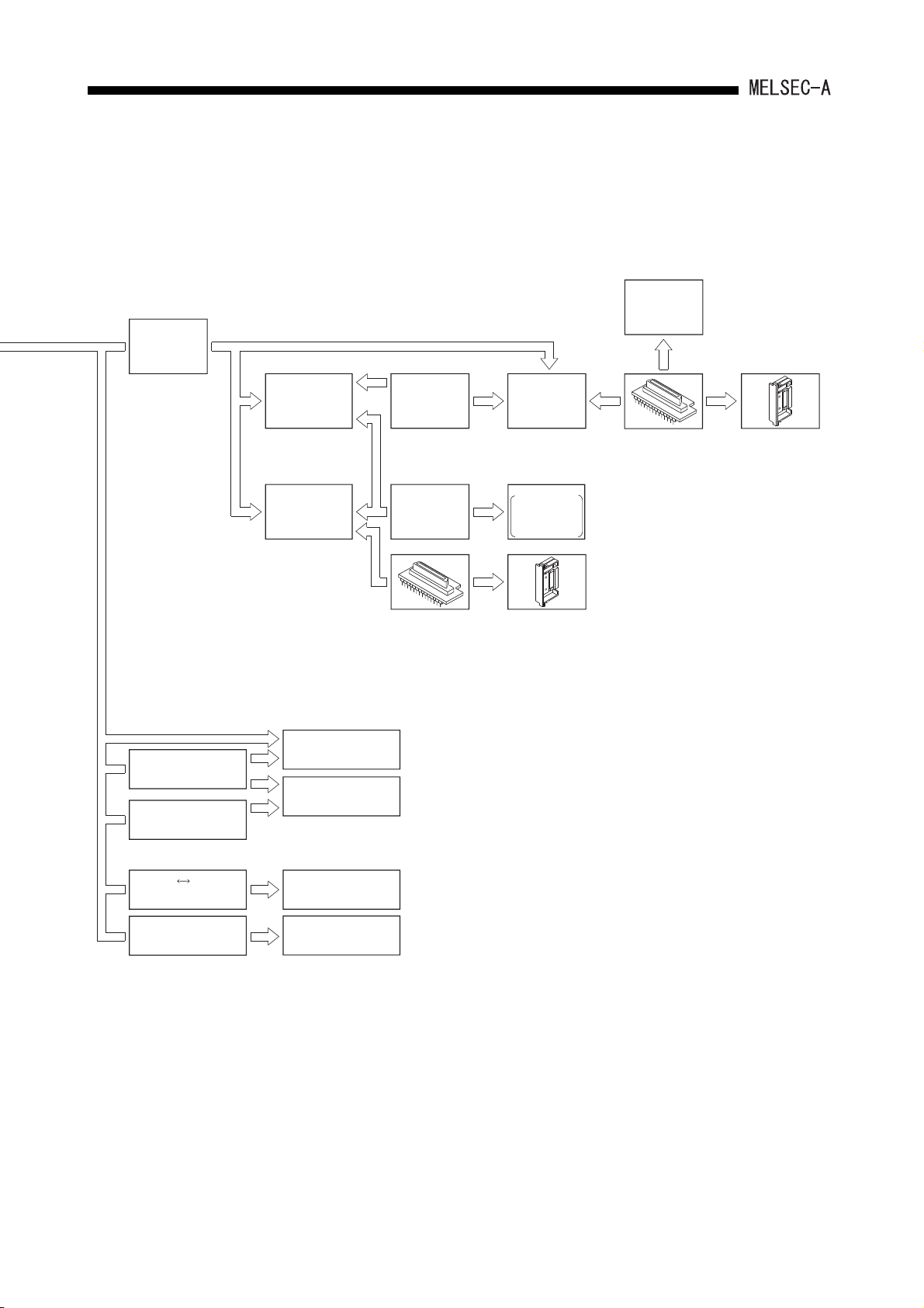
SYSTEM CONFIGURATION2.
(To A1SJHCPU(S8))
AC30R4
AC300R4
cable
AC30R4-PUS
cable
AC20R4-A8PU
cable
A6PHP
Plasma hand-held
graphic programmer
A6GPP
intelligent GPP
A7PUS
programming module
A8PUE
programming module
AC03WU
cable
AC30R2
cable
EP-ROM write adapter
(A6WA-28P)
A6WU
P-ROM writer
module
Printer
A7NPR-S1,
K6PR-K,
general-purpose
printer
ROM cassette
(A1SNMCA-8KP)
ROM writer
EP-ROM write
adapter
(A6WA-28P)
*
ROM cassette
(A1SNMCA-8KP)
RS-232C RS-422
conerter
AC30R4-PUS
cable
*1, *2
IBM PC/AT or
100% compatible
A6DU-B
data access module
*1:
Refer to SW0IX-GPPAE Software
Package Operating Manual or the
MELSEC-MEDOC Operating Manual for
connectable cables and devices.
*2:
IBM is a registered trademark of the
International Buisiness Machines Corporation.
2 - 4
Page 26

2. SYSTEM CONFIGURATION
2.2 Precautions when Configuring the System
The hardware and software packages which can be used for the CPU module are
described.
2.2.1 Hardware
(1) I/O module
All the building-block-type I/O modules for A N and A A can be used by installing
them to the extension base module of A5 B/A6 B.
2 - 5
Page 27
SYSTEM CONFIGURATION2.
(2) Special function module
(a) Special function modules for A N and A A can be used by installing them in
the extension base of A5 B/A6 B.
(b) Installation count of the following modules are limited of the special function
modules.
AD51H-S3
AJ71UC24
AJ71E71N-B5
AJ71C23-S3
AJ61BT11 (Only when the intelligent mode is used.)
GOT-A900 Series (Only when the bus connection is
*1
used.)
GOT1000 Series (Only when the bus connection is
*1
used.)
A1SJ71UC24-R2(PRF/R4)
A1SJ71E71N-B2
A1SJ71E71N-B5T
A1SD51S A1SD21-S1
A1SJ61BT11 (Only when the intelligent mode is
used.)
AI61(S1)
A1SI61
AJ71AP21(S3)
AJ71AT21B
A1SJ71AP21(S3)
A1SJ71AT21B
AJ71LP21(G/GE)
AJ71LR21
AJ71C22-S1
AJ71E71N-B2
AJ71E71N-T
AD22-S1
AJ71AR21
A1SJ71AR21
AJ71BR11
Up to 2 modules in total can be installed.
Only one module can be installed.
Only one module can be installed.
A1SJ71LP21(GE)
A1SJ71LR21
AJ71PT32-S3 (Only when the extension mode is
used.)
AJ71T32-S3 (Only when the extension mode is
used.)
A1SJ71PT32-S3 (Only when the extension mode is
used.)
A1SJ71T32-S3 (Only when the extension mode is
used.)
*1 Refer to the following manual for the GOT model names.
GOT-A900 Series User's Manual (GT Work2 Version2/GT Designer2 Version2 Compatible
Connection System Manual)
GOT1000 Series Connection Manual
A1SJ71BR11
2 - 6
Only one module can be installed.
Page 28
SYSTEM CONFIGURATION2.
POINT
When the dedicated instruction for
the CC-Link is used, use the master
module marked "9707 B" or later in
MITSUB ISHI
CPU UNIT
MODEL
A2USHCPU-S1
MAX 30kSTEP
DATE
9707 B
the DATE column of the rated plate.
MITSUBISHI ELECTRIC
BD992D008H38
Function version
Date of manufacture
(3) Peripheral device
(a) Precautions when using an A6WU P-ROM writer
1) When using an A1SHCPU
Use an A6WU P-ROM writer module whose software version is E or later.
(b) The A6WU P-ROM writer module cannot be installed with add-on system, which
is installed directly in the AnSHCPU.
Only hand-held system, which is installed using cables, is possible.
(c) Among the programming modules (A7PUS and A8PUE), only the A7PUS can be
installed with add-on system.
Other models (A8PUE) can be installed with hand-held system, which is
connected with cables.
2 - 7
Page 29
SYSTEM CONFIGURATION2.
(4) EP-ROM memory cassette ROM partition
Partitioning the EP-ROM memory cassette with an A6GPP (SW4GP-GPPA)/A6WU
requires a memory write adapter (optional).
The following shows the valid combinations of memory cassette and memory write
adapter:
CPU Model
A1SHCPU A1SNMCA-8KP 32k bytes
A1SJHCPU(S8) A1SNMCA-8KP 32k bytes
(5) Program write during operation with E
(a) When an operation is executed using an E
Memory Cassette
Model Capacity
2
PROM
Memory Write Adapter Model
A6WA-28P
2
PROM, write during RUN is not
possible. If write during RUN is executed, the following messages are displayed
on the peripheral devices:
For SW3GP-GPPA: "PLC COMMUNICATIONS ERROR : ERROR
CODE = 19"
For SW0RX-GPPA: "PLC COMMUNICATIONS ERROR :ERROR
CODE = 19"
For A7PUS: "PLC NOT RESPOND"
(b) The writing of the program cannot be executed from the computer link module or
from a peripheral device connected to other stations on the MELSECNET.
Write programs from peripheral devices connected to the AnSHCPU's RS-422.
2 - 8
Page 30
2. SYSTEM CONFIGURATION
2.2.2 Software package
(1) GPP function software packages and model name setting at the start-up
(a) For AnSHCPU start-up, use the PLC model "A3".
(b) Perform the PLC type setting as shown below when using conventional
peripheral devices.
Peripheral
Device
Software Package for System
Start-u p
Programmable controller CPU
Model for Set-up
A1SJH
/A1SH
A2SH A2SH-S1
Remark
IBM PC/AT
SW IVD-GPPA
MELSEC MEDOC
*
A3
*
A3 A3
MELSEC MEDOC plus
A1SJH/
A1SH
A2SH A2SH-S1
A3
Writing on the ROM
is not allowed.
A6PHP
GX Developer
SW3GP-GPPA
SW4GP-GPPA
A3* A3
A6GPP SW3-GPPA
SW3GP-GPPA
A3
Writing on the ROM
is not allowed.
SW4GP-GPPA
*Select the model names according to the software package versions as shown below:
Model Name
Type
Select "A0J2H" Select "A1S" Select "A1SH" Select "A3" Select "A1SH"
SW4GP-GPPA Q or earlier R or later All versions
SW3RXV-GPPA 30D or earlier 40E or later 30D or earlier 40E or later
SW3NX-GPPA 60G or earlier 70H or later 60G or earlier 70H or later
SW3IVD-GPPA 60G or earlier 70H or later 60G or earlier 70H or later
For ROM Writing For Programming
2 - 9
Page 31

SYSTEM CONFIGURATION2.
POINT
(1) Old software packages other than SW3-GPPA, SW3GP-GPPA, and SW4GP-
GPPA cannot be used as the software package for system start-up for
A6GPP/A6PHP.
(2) Take caution when using a software version that selects "A0J2H" or "A1S" for
ROM writing, since the file register area of 8k points is reduced to 4k points.
To measure this, use a software package for which A1SJH/A1SH can be
selected.
(2) Utility package
(a) The following shows the applicable utility packages:
SW0GHP-UTLPC-FN1 SW0GHP-UTLPC-PID SW0GHP-UTLP-FD1
SW0GHP-UTLPC-FN0 SW0C-UTLP-FN0 SW1GP-AD57P
SW0-AD57P
[1] Select "A3CPU" when a SW0GHP-UTLPC-FN1 or a SW0GHP-UTLP-
FD1 is started up.
[2] If both a SW1GP-AD57P and another utility package are used in
combination, specify "AD57P-COM" as the file name.
(b) The following shows the inapplicable utility package model:
SW0-SAPA(MELSAP)
2 - 10
Page 32

2. SYSTEM CONFIGURATION
2.3 System Equipment
The following shows the system equipment (modules and peripheral devices) that can be
used in an AnS system.
(1) AnS series modules
Product Name Model Name Description
Number of I/O points: 256, memory capacity: 64k
bytes,
Number of I/O slots: 5
Number of I/O points: 256, memory capacity: 64k
bytes,
Number of I/O slots: 8
Number of I/O points: 256, memory capacity: 64k
bytes,
Number of I/O points: 512, memory capacity: 256k
bytes
bytes
CPU module
Power supply
module
A1SJHCPU
A1SJHCPU
(S8)
A1SHCPU
A2SHCPU
A2SHCPU-S1Number of I/O points: 1024, memory capacity: 192k
A1S61PN 5VDC, 5A
A1S62PN 5VDC, 3A/24VDC, 0.6A
A1S63P 5VDC, 5A 24VDC input
100/200VAC
input
Number of occupied points
(points)
[I/O Assignment
Module Type]
–0.30–
–0.30–
–0.30–
–0.40–
–0.40–
–––
Current
Consumption
5VDC(A) 24VDC(A)
Remark
Built-in RAM
memory
Installed in the
power supply slot
of the main base
and extension
base.
2 - 11
Page 33

SYSTEM CONFIGURATION2.
Product Name Model Name Description
A1SX10 16-point 100 to 120 VAC input module 16 [16 input points] 0.05 –
A1SX10EU 16-point 100 to 120VAC input module 16 [16 input points] 0.05 –
A1SX20 16-point 200 to 240VAC input module 16 [16 input points] 0.05 –
A1SX20EU 16-point 200 to 240VAC input module 16 [16 input points] 0.05 –
A1SX30 16-point 12/24VDC, 12/24VAC input module 16 [16 input points] 0.05 –
A1SX40 16-point 12/24VDC input module 16 [16 input points] 0.05 –
A1SX40-S1 16-point 24VDC input module 16 [16 input points] 0.05 –
A1SX40-S2 16-point 24VDC input module 16 [16 input points] 0.05 –
A1SX41 32-point 12/24VDC input module 32 [32 input points] 0.08 –
A1SX41-S1 32-point 24VDC input module 32 [32 input points] 0.12 –
Input module
A1SX41-S2 32-point 24VDC input module 32 [32 input points] 0.08 –
A1SX42 64-point 12/24VDC input module 64 [64 input points] 0.09 –
A1SX42-S1 64-point 24VDC input module 64 [64 input points] 0.16 –
Number of occupied points
(points)
[I/O Assignment
Module Type]
Current
Consumption
5VDC(A) 24VDC(A)
Remark
A1SX42-S2 64-point 24VDC input module 64 [64 input points] 0.09 –
A1SX71 32-point 5/12/24VDC input module 32 [32 input points] 0.075 –
A1SX80 16-point 12/24VDC sink/source input module 16 [16 input points] 0.05 –
A1SX80-S1 16-point 24VDC sink/source input module 16 [16 input points] 0.05 –
A1SX80-S2 16-point 24VDC sink/source input module 16 [16 input points] 0.05 –
A1SX81 32-point 12/24VDC sink/source input module 16 [16 input points] 0.08 –
A1SX81-S2 32-point 24VDC sink/source input module 32 [32 input points] 0.08 –
A1SX82-S1 64-point 24VDC sink/source input module 32 [32 input points] 0.16 –
*1:0.08A is shown on the rating plate of the module.
2 - 12
Page 34

SYSTEM CONFIGURATION2.
Product Name Model Name Description
A1SY10 16-point relay contact output module (2A) 16 [16 output points] 0.12 0.09
A1SY10EU 16-point relay contact output module (2A) 16 [16 output points] 0.12 0.10
A1SY14EU 12-point relay contact output module (2A) 16 [16 output points] 0.12 0.10
A1SY18A
A1SY18AEU
A1SY22 16-point triac output module (0.6A) 16 [16 output points] 0.27
A1SY28A
A1SY40
A1SY40P
A1SY41
8-point relay contact output module (2A) for
independent contacts
8-point relay contact output module (2A) for
independent contacts
8-point triac output module (1A)
All points independent
16-point 12/24VDC transistor output module
(0.1A) sink type
16-point 12/24VDC transistor output module (0.1A)
sink type
32-point 12/24VDC transistor output module
(0.1A) sink type
Number of occupied points
(points)
[I/O Assignment
Module Type]
16 [16 output points] 0.24 0.075
16 [16 output points] 0.24 0.075
16 [16 output points] 0.13 –
16 [16 output points] 0.27 0.008
16 [16 output points]
32 [32 output points] 0.50 0.008
Current
Consumption
5VDC(A) 24VDC(A)
(200VAC)
0.002
*2
0.079
0.011
Remark
Output module
A1SY41P
A1SY42
A1SY50
A1SY60
A1SY60E
A1SY68A
A1SY71
A1SY80
A1SY81
A1SY82
32-point 12/24VDC transistor output module (0.1A)
sink type
64-point 12/24VDC transistor output module
(0.1A) sink type
16-point 12/24VDC transistor output module
(0.5A) sink type
16-point 24VDC transistor output module
(2A) sink type
16-point 12/24VDC transistor output module
(2A) source type
8-point 5/12/24/48VDC
transistor output module (2A) sink/source type
All points independent
32-point 5/12VDC transistor output module
(0.016A) sink type
16-point 12/24VDC transistor output module
(0.8A) source type
32-point 12/24VDC transistor output module
(0.1A) source type
64-point 12/24VDC transistor output module
(0.1A) source type
*3
32 [32 output points]
64 [64 output points] 0.93 0.008
16 [16 output points] 0.12 0.06
16 [16 output points] 0.12 0.015
16 [16 output points] 0.20 0.01
16 [16 output points] 0.11 –
32 [32 output points] 0.40 0.15
16 [16 output points] 0.12 0.02
32 [32 output points] 0.50 0.008
64 [64 output points] 0.93 0.008
0.141
0.012
*2:0.08A is shown on the rating plate of the module.
*3:0.15A is shown on the rating plate of the module.
2 - 13
Page 35

SYSTEM CONFIGURATION2.
Product Name Model Name Description
32-point 12/24VDC input module
I/O hybrid
module
Dynamic input
module
A1SH42
A1SH42P
A1SH42-S1
A1SH42P-S1
A1SX48Y18
A1SX48Y58
A1S42X
32-point 12/24VDC transistor output module
(0.1A) sink type
32-point 12/24VDC input module
32-point 12/24VDC transistor output module
(0.1A) sink type
32-point 24VDC input module
32-point 12/24VDC transistor output module
(0.1A) sink type
32-point 24VDC input module
32-point 12/24VDC transistor output module
(0.1A) sink type
8-point 24VDC input module
8-point relay contact output module (2A)
8-point 24VDC input module
8-point 12/24VDC transistor output module (0.5A)
16/32/48/64 points
12/24VDC dynamic input module
Number of occupied points
(points)
[I/O Assignment
Module Type]
32 [32 output points] 0.50 0.008
32 [32 output points] 0.13 0.012
32 [32 output points] 0.50 0.008
32 [32 output points] 0.13 0.012
16 [16 output points]
16 [16 output points] 0.06 0.06
Specified number of points
[Input
Specified number of points
Current
Consumption
5VDC(A) 24VDC(A)
*4
0.085
0.08 –
]
0.045
Remark
Dynamic output
module
*4:0.09A is shown on the rating plate of the module.
A1S42Y
16/32/48/64 points
12/24VDC dynamic output module
Specified number of points
[Output
Specified number of points
0.18 0.055
]
2 - 14
Page 36

SYSTEM CONFIGURATION2.
Number of occupied points
Product Name Model Name Description
Blank cover A1SG60 Dust-proof cover for unused slot 16 [Empty] – –
Specified number of points
[Input
Specified number of points
16 [16 output points]
16 [16 output points]
32
32
32
Dummy module A1SG62
Pulse catch
module
Analog timer
module
Interrupt
module
A1SP60
A1ST60
A1SI61
A1SD61
A1SD62
16-point, 32-point, 48-point, 64-point selectable
module
Short ON-time pulse input module
(pulse with a minimum of 0.5ms) 16 input points
A module whose timer setting value can be
changed for different volumes (0.1 to 1.0s1 to
10s10 to 60s60 to 600s)
Analog timer 8 points
Interrupt module for specifying the interrupt
program
(16-point interrupt input)
32-bit signed binary
50kPPS, 1 channel
24-bit signed binary, 2 channel
100kPPS, DC input,
transistor output (sink type)
(points)
[I/O Assignment
Module Type]
[32 special
points]
[32 special
points]
[32 special
points]
Current
Consumption
5VDC(A) 24VDC(A)
––
]
*5
0.055
*5
0.055
*5
0.057
0.35 –
0.1 –
Remark
–
–
–
High-speed
counter module
A/D converter
module
D/A converter
module
Analog I/O
module
A1SD62D
A1SD62D-S1
A1SD62E
A1S64AD
A1S68AD
A1S62DA
A1S68DAV
A1S68DAI
A1S63ADA
A1S66ADA
24-bit signed binary, 2 channel
200kPPS, difference input,
transistor output (sink type)
24-bit signed binary, 2 channel
200kPPS, difference input,
transistor output (sink type)
24-bit signed binary, 2 channel
100kPPS, DC input,
transistor output (source type)
4 to 20mA/0 to 10V
4 analog channels
4 to 20mA/0 to 10V
8 analog channels
4 to 20mA/0 to 10V
2 analog output channels
-10 to 10V input
8 analog output channels
4 to 20mA input
8 analog output channels
Analog input, 2 channels, simple loop control is
allowed
1 analog output channels
Analog input, 4 channels, simple loop control is
allowed
2 analog output channels
32
32
32
32
32
32
32
32
32
64
[32 special
points]
[32 special
points]
[32 special
points]
[32 special
points]
[32 special
points]
[32 special
points]
[32 special
points]
[32 special
points]
[32 special
points]
[64 special
points]
0.25 –
0.27 –
0.1 –
0.4 –
0.4 –
0.8 –
0.65 –
0.85 –
0.8 –
0.21 0.16
*5:0.06A is shown on the rating plate of the module.
2 - 15
Page 37

SYSTEM CONFIGURATION2.
Product Name Model Name Description
For connecting to Pt100 (3-wire)
Temperature input, 2 channels
For connecting to Pt100 (4-wire)
Temperature input, 2 channels
Transistor output, thermocouple input
2 channels/modules
PID control: ON/OFF pulse
Transistor output, thermocouple input
2 channels/modules
PID control: ON/OFF pulse, wire breakage
detection function
Transistor output, platinum temperature-mesuring
resistor input
2 channels/modules
PID control: ON/OFF pulse
Transistor output, platinum temperature-mesuring
resistor input
2 channels/modules
PID control: ON/OFF pulse, wire breakage
detection function
Transistor output, thermocouple input
4 channels/modules
PID control: ON/OFF pulse or 2 positioning control
Temperature
regulating
module
A1S62RD3
A1S62RD4
A1S68TD Thermocouple input, 8 channels 32
A1S62TCTTS2
A1S62TCTT
BW-S2
A1S62TCRTS2
A1S62TCRT
BW-S2
A1S64TCTTS1
Number of occupied points
(points)
[I/O Assignment
Module Type]
32
32
32
32
32
32
32
[32 special
points]
[32 special
points]
[32 special
points]
[32 special
points]
[32 special
points]
[32 special
points]
[32 special
points]
[32 special
points]
Current
Consumption
5VDC(A) 24VDC(A)
0.49 –
0.39 –
0.32 –
0.19 –
0.28 –
0.19 –
0.28 –
0.33 –
Remark
A1S64TCTT
BW-S1
A1S64TCRTS1
A1S64TCRT
BW-S1
A1S64TCTR
T
A1S64TCTR
TBW
Transistor output, thermocouple input
4 channels/modules
PID control: ON/OFF pulse or 2 positioning control
Heater wire breakage detection function
Transistor output, thermocouple input
4 channels/modules
PID control: ON/OFF pulse or 2 positioning control
Transistor output, thermocouple input
4 channels/modules
PID control: ON/OFF pulse or 2 positioning control
Heater wire breakage detection function
Transistor output, thermocouple/platinum
temperature-mesuring resistor input.
4 channels/modules
PID control: ON/OFF pulse or 2 positioning
control
Transistor output, thermocouple/platinum
temperature-mesuring resistor input.
4 channels/modules
PID control: ON/OFF pulse or 2 positioning
control
Heater break detection function
32
32
32
32
32
[32 special
points]
[32 special
points]
[32 special
points]
[32 special
points]
[32 special
points]
0.42 –
0.33 –
0.42 –
0.33 –
0.39 –
2 - 16
Page 38

SYSTEM CONFIGURATION2.
Product Name Model Name Description
Computer link
module
Ethernet
interface
module
Intelligent
communication
module
A1SJ71UC24
-R2
A1SJ71UC24
-PRF
A1SJ71UC24
-R4
A1SJ71E71N
3-T
A1SJ71E71N
-T
A1SJ71E71N
-B2
A1SJ71E71N
-B5
A1SD51S
Computer link function RS-232C, 1 channel 32
Computer link function, printer function
RS-232C, 1 channel
Computer link function, multidrop link function
RS-422/RS-485, 1 channel
10 Base-T 32
10 Base-T 32
10 Base 2 (for Cheapernet) 32
10 Base 5 (for Ethernet) 32
BASIC (interpreter/compiler)
RS-232C, 2 channels
RS-422/RS-485, 1 channel
Number of occupied points
(points)
[I/O Assignment
Module Type]
[32 special
points]
32
32
32
[32 special
points]
[32 special
points]
[32 special
points]
[32 special
points]
[32 special
points]
[32 special
points]
[32 special
points]
Current
Consumption
5VDC(A) 24VDC(A)
0.1 –
0.1 –
0.1 –
0.69 –
0.56 –
0.66 –
0.57 –
0.4 –
Remark
Accessible within
the AnACPU
device range
Positioning
module
ID
interface
module
A1SD70
A1SD75P1S3
A1SD75P2S3
A1SD75P3S3
A1SD75M1
A1SD75M2
A1SD75M3
A1SD35ID1
A1SD35ID2
1 axis positioning control, speed control, analog
voltage output for speed-positioning control 0 to
10V)
For positioning control, pulse output, 1 axis 32
For positioning control, pulse output, 2 axes (2-axis
simultaneous, linear interpolation, circular
interpolation)
For positioning control, pulse output, 3 axes
(Independent, 3-axis simultaneous, linear
interpolation, circular interpolation)
For positioning control, digital output, for MR-H-B/
MR-J-B/MR-J2-B, 1-axis SSCNET
For positioning control, digital output, for MR-H-B/
MR-J-B/MR-J2-B, 2-axis SSCNET (independent, 2axis simultaneous, linear interpolation, circular
interpolation)
For positioning control, digital output, for MR-H-B/
MR-J-B/MR-J2-B, 3-axis SSCNET (independent, 3axis simultaneous, 2-axis linear interpolation, 2-axis
circular interpolation)
ID interface module
One reader/writer modules can be connected.
ID interface module
Two reader/writer modules can be connected.
48
First half
Second
32
32
32
32
32
32
32
16 empty points
half
32 special points
[32 special
points]
[32 special
points]
[32 special
points]
[32 special
points]
[32 special
points]
[32 special
points]
[32 special
points]
[32 special
points]
0.3 –
0.7 –
0.7 –
*
0.7
0.7 –
0.7 –
0.7 –
0.25 0.17
0.25 0.33
–
* When different
driver is
connected: 0.78A
2 - 17
Page 39

SYSTEM CONFIGURATION2.
Product Name Model Name Description
For the master and local stations of
MELSECNET(II)
data link
module
MELSECNET/B
data link
module
B/NET
interface
module
A1SJ71AP21
A1SJ71AP21
-S3
A1SJ71AR21
A1SJ71AT21BFor the master and local stations of MELSECNET/
A1SJ72T25B
A1SJ71B62S3
A1SJ71LP21
MELSECNET(II) data link system (for the optical
fiber cable)
For the master and local stations of
MELSECNET(II) data link
(for the GI-type optical fiber cable)
For the master and local stations of
MELSECNET(II) data link system (for the coaxial
cable)
B data link system
For the remote I/O station of
MELSECNET/B data link system
Master module for B/NET 32
For the control, master, and normal stations of the
MELSECNET/10 data link module system
(For the coaxial cable dual loop)
Number of occupied points
(points)
[I/O Assignment
Module Type]
32
32
32
32
32
[32 special
points]
[32 special
points]
[32 special
points]
[32 special
points]
–0.3–
[32 special
points]
[32 special
points]
Current
Consumption
5VDC(A) 24VDC(A)
0.33 –
0.33 –
0.8 –
0.66 –
0.08 –
0.65 –
Remark
Access is allowed
within the device
range of the
AnACPU.
MELSECNET/
10 data link
module
CC-Link system
master module
MELSECNET/
MINI-S3 master
module
MELSECNETI/O LINK
master module
S-LINK
interface
module
A1SJ71LP21
GE
A1SJ71BR11
A1SJ71LR21
A1SJ61BT11
A1SJ71PT32
-S3
A1SJ51T64
A1SJ71SL92NMaster module for S-LINK
For the control, master, and normal stations of the
MELSECNET/10 data link module system
(For the GI-type optical fiber cable dual loop)
For the control, master, and normal stations of the
MELSECNET/10 data link module system
(For the single bus coaxial cable)
For the control, master, and normal stations of the
MELSECNET/10 data link module system
(For the coaxial cable dual loop)
For the master and local stations of the CC-Link
data link system
(For the twisted pair shield cable only)
For MELSECNET/MINI-S3 master stations (max.
64 stations). Performs remote I/O and remote
terminal control of a total of 512 I/O points.
MELSECNET-I/O LINK master station.Controls I/O
LINK remote I/O module of a maximum of 16
stations and a total of 128 I/O points.
I/O total 128 points
32
32
32
32
I/O mode
[32 special points]
Expanded mode
48 [48 special points]
64
32
[32 special
points]
[32 special
points]
[32 special
points]
[32 special
points]
[64 special
points]
[32 special
points]
0.65 –
0.80 –
1.14 –
0.40 –
0.35 –
0.115 0.09
0.20 –
AS-I interface
module
Positioning
detection
module
*6:0.06A is shown on the rating plate of the module.
A1SJ71AS92
A1S62LS Absolute positioning detection module 32
Master module for AS-I
I/O total 496 points
2 - 18
32
[32 special
points]
[32 special
points]
0.15 –
0.55 –
Page 40

SYSTEM CONFIGURATION2.
Product Name Model Name Description
PC easier
monitoring
module
Memory card
interface
module
Simulation
module
PROFIBUS
interface
module
Device Net
interface
module
A1SS91 PC easier monitoring module 16
A1SD59J-S2 Memory card interface module 32
An I/O simulation unit used connected to the base
module.Debugging can be executed without
A6SIMX64Y64
A1SJ71PB92
D
A1SJ71PB96
F
A1SJ71DN91 Device net master module 32
connecting the I/O module to the base module.Use
an expansion cable of the AnS series between the
main base of the AnS series and the A6SIM-
X64Y64.
PROFIBUS-DPmaster module 32
PROFIBUS-FMS interface module 32
Number of occupied points
(points)
[I/O Assignment
Module Type]
[16 special
points]
[32 special
points]
64
64
[64 input points]
[64 output points]
[32 special
points]
[32 special
points]
[32 special
points]
Current
Consumption
5VDC(A) 24VDC(A)
0.08 –
0.05 –
TYP. 0.3
(When
all points
ON)
0.56 –
0.56 –
0.24 –
–
Remark
The current consumption
describes in
connecting
A1SD59J-MIF.
MODBUS
interface
module
A1SJ71UC24
-R2-S2
A1SJ71UC24
-R4-S2
RS-232Ctype MODBUS interface module 32
RS-422/485type MODBUS interface module 32
[32 special
points]
[32 special
points]
0.1 –
0.1 –
2 - 19
Page 41

SYSTEM CONFIGURATION2.
Product Name Model Name Description
A985GOT
A975GOT
A970GOT
A960GOT
A956GOT
A956WGOT
Graphic
operation
terminal
A953GOT
Large-size graphic operation terminal
256 colors, TFT color, 800 600 dots, high intensity
Large-size graphic operation terminal
256 colors, TFT color, 640 480 dots, high intensity
Large-size graphic operation terminal
16 colors, TFT color, 640 480 dots, high intensity/
16 colors, TFT color, 640 480 dots, wide viewing
angle/
8 colors, STN color, 640 480 dots/
2 colors, STN monochrome, 640 480 dots
Large-size graphic operation terminal
2 colors, EL, 640 400 dots
Medium-size graphic operation terminal
8 colors, STN color, 320 240 dots/
STN monochrome, 320 240 dots/
256 colors, TFT color 320 240 dots
Medium-size graphic operation terminal
256 colors, TFT color 480 234 dots
Medium-size graphic operation terminal
8 colors, STN color, 320 240 dots/
STN monochrome, 320 240 dots/
256 colors, TFT color 320 240 dots
Number of occupied points
(points)
[I/O Assignment
Module Type]
32
[32 special
points]*
–––
Current
Consumption
5VDC(A) 24VDC(A)
0.22 * –
Remark
*When bus
connected
For RS-232C
connected only
Main base unit
Medium-size graphic operation terminal
A951GOT
A950GOT
GT1565VTBA
GT1575VTBA
A1S32B 2 I/O modules can be installed.
A1S33B 3 I/O modules can be installed.
A1S35B 5 I/O modules can be installed.
A1S38B 8 I/O modules can be installed.
8 colors, STN color, 320 240 dots/
STN monochrome, 320 240 dots/
256 colors, TFT color 320 240 dots
Medium-size graphic operation terminal
8 colors, STN color, 320 240 dots/
STN monochrome, 320 240 dots/
256 colors, TFT color 320 240 dots
Large-size graphic operation terminal 8.4"
256/65536 colors, TFT color, 640 480 dots
(When installing a multi color display board, 65536
colors can be displayed.)
Large-size graphic operation terminal 10.4"
256/65536 colors, TFT color, 640 480 dots
(When installing a multi color display board, 65536
colors can be displayed.)
32
[32 special
points]*
–––
[32 special
points]*
–––
0.22 * –
0.12 –
32
*When bus
connected
For RS-422
connected only
*When bus
connected
Extension
connector on the
right and left side
each.
2 - 20
Page 42

SYSTEM CONFIGURATION2.
Product Name Model Name Description
Extension base
unit
Extension cable
A1S52B
A1S52B-S1
A1S55B
A1S55B-S1
A1S58B
A1S58B-S1
A1S65B
A1S65B-S1
A1S68B
A1S68B-S1
A1SC01B 55mm (2.17inch) long flat cable – – –
A1SC03B 330mm (13inch) long
A1SCO7B 700mm (27.56inch) long
A1SC12B 1200mm (47.24inch) long
A1SC30B 3000mm (118.11inch) long
A1SC60B 6000mm (236.22inch) long
2 I/O modules can be installed.
5 I/O modules can be installed.
8 I/O modules can be installed. – – –
5 I/O modules can be installed.
8 I/O modules can be installed.
Number of occupied points
(points)
[I/O Assignment
Module Type]
–––
–––
–––
Current
Consumption
5VDC(A) 24VDC(A)
Remark
The power supply
module cannot be
installed.
(Power is
supplied from the
main base unit.)
The power supply
module is
required.
For extension
towards right
Connection cable
for the extension
base unit.
A1SC05NB 450mm (17.72inch) long
A1SCO7NB 700mm (27.56inch) long
A1SC30NB 3000mm (118.11inch) long
A1SC50NB 5000mm (196.86inch) long
Cable for the
–––
AN, AA
extension base
unit
2 - 21
Page 43

SYSTEM CONFIGURATION2.
Product Name Model Name Description Applicable Model
EP-ROM A1SNMCA-8KP 8k steps, equipped with EP-ROM(directly) For A1SJH/A1SHCPU: A6WA-28P required
A1SNMCA-2KE
Memory
cassette
Memory write
adapter
Battery A6BAT IC-RAM memory backup
Connector/terminal
block converter unit
E
A1SNMCA-8KE
2
PROM
A2SNMCA30KE
A6WA-28P
A6TBXY36
A6TBXY54
A6TBX70 For the sink-type input module (3-wire type)
A6TBX36-E For the source-type input module (standard type) A1SX71, A1SX82-S1, A1SX81(S2)
A6TBY36-E For the source-type output module (standard type) A1SY81, A1SY82
A6TBX54-E For the source-type input module (2-wire type) A1SX71, A1SX82-S1, A1SX81(S2)
A6TBY54-E For the source-type output module (2-wire type) A1SY81, A1SY82
2k steps, equipped with E
8k steps, equipped with E
With 30k-step E
Used for memory cassette connector/EP-ROM 28pin adapter
For the sink-type input module and sink-type output
module. (standard type)
For the sink-type input module and sink-type output
module. (2-wire type)
2
PROM (directly)
2
PROM (directly)
2
PROM (directly)
Write/read directly from the peripheral device for A1SJH/
A1SHCPU is possible.
Direct writing to and reading from a peripheral device is
feasible.
Used for ROM writing in A1SNMCA-8KP
Installed in the A1SJHCPU(S8), A1SHCPU,
A2SHCPU(S1) main unit
A1SX41(S1/S2), A1SX42(S1/S2), A1SY41, A1SY41P,
A1SY42, A1SY82, A1SH42(S1), A1SH42P(S1)
A1SX41(S1/S2),A1SX42(S1/S2),A1SH42(S1),
A1SH42P(S1)
A6TBX70-E For the source-type input module (3-wire type) A1SX71, A1SX82-S1, A1SX81(S2)
AC05TB 0.5m (1.64ft.) for the sink module
AC10TB 1m (3.28ft.) for the sink module
AC20TB 2m (6.56ft.) for the sink module
AC30TB 3m (9.84ft.) for the sink module
AC50TB 5m (16.40ft.) for the sink module
Cable for
connector/terminal
block converter unit
Relay terminal unit A6TE2-16SRN For the sink-type output module A1SY41, A1SY41P, A1SY42, A1SH42(S1), A1SH42P(S1)
AC80TB 8m (26.24ft.) for the sink module
AC100TB 10m (32.81ft.) for the sink module
AC05TB-E 0.5m (1.64ft.) for the source module
AC10TB-E 1m (3.28ft.) for the source module
AC20TB-E 2m (6.56ft.) for the source module
AC30TB-E 3m (9.84ft.) for the source module
AC50TB-E 5m (16.40ft.) for the source module
A6TBXY36
A6TBXY54
A6TBX70
A6TBX36-E
A6TBY36-E
A6TBX54-E
A6TBY54-E
A6TBX70-E
2 - 22
Page 44

SYSTEM CONFIGURATION2.
Product Name Model Name Description Applicable Model
AC06TE 0.6m (1.97ft.) long
Cable for
connecting the
relay terminal unit
Terminal block
cover for the A1S
I/O module and the
special module
IDC terminal block
adapter
Terminal block
adapter
40-pin connector
AC10TE 1m (3.28ft.) long
AC30TE 3m (9.84ft.) long
AC50TE 5m (16.40ft.) long
AC100TE 10m (32.81ft.) long
A1STEC-S
A1S-TA32
A1S-TA32-7
A1S-TB32
A6CON1 Soldering-type, straight out
A6CON2 Crimp type, straight out
A6CON3 Insulation-displacement type, flat cable
Slim-type terminal block cover for the A1S I/O
module and the special module (terminal block
connector type).
IDC terminal block adapter for 32 points 0.5mm
(AWG20)
IDC terminal block adapter for 32 points 0.3mm
(AWG22)
IDC terminal block adapter for 32 points 0.75mm
(AWG18)
For 32 points, conversion into Europe type terminal
block
A6TE2-16SRN
All terminal block connector type modules
2
2
A1SX41(S1/S2), A1SX71, A1SY41, A1SY71A1S-TA32-3
2
A1SX41(S1/S2), A1SX71, A1SY41, A1SY41P, A1SY71
Sink type (40p FCN)
3-pin D-sub
connector
A6CON4 Soldering-type, straight/diagonal out
A6CON1E Soldering-type, straight out
Source type (37p D-sub)A6CON2E Crimp type, straight out
A6CON3E Insulation-displacement type, flat cable
REMARK
Toa Electric Industrial CO., LTD. provides I/O cables with connectors, which can
connect to 40-pin connector (A1SX41, A1SX42, A1SY41, A1SY41P, A1SY42,
A1SY42P, etc.) or 37-pin D-sub connector (A1SX81, A1SY81) of I/O modules.
Contact:
TOA ELECTRIC INDUSTRIAL CO., LTD.
2 - 23
Page 45

SYSTEM CONFIGURATION2.
(2) Peripheral device
Product Name Model Name Remark
• A6PHP main unit
Plasma hand-held
graphic programmer
Intelligent GPP A6GPP-SET
Composite video cable AC10MD • Connection cable for the monitor display of the A6GPP screen: 1m (3.28 ft.) long
A6PHP-SET
• SW GP-GPPA........
• SW GP-GPPK........
• SW0-GPPU...............
• AC30R4....................
• A6GPP main unit
• SW GP-GPPA.........
• SW GP-GPPK.........
• SW0-GPPU................
• AC30R4.....................
GPP function start-up floppy disk for the A series
GPP function start-up floppy disk for the K series
User floppy disk (2DD)
RS-422 cable 3m (9.84 ft.)-long
GPP function start-up floppy disk for the A series.
GPP function start-up floppy disk for the K series.
User floppy disk (2DD).
RS-422 cable 3m (9.84 ft.)-long
RS-422 cable
User floppy disk SW0S-USER 2HD-type
Floppy disk for cleaning SW0-FDC For A6GPP/A6PHP Floppy disk for cleaning the floppy disk drive.
Optional keyboard for
A6PHP
Optional keyboard for
A6GPP
AC30R4 3m (9.84ft.) long
AC300R4 30m (98.43ft.) long
• A6KB keyboard
A6KB-SET-H
A6KB-SET
• AC03R4H..............
• A6KB-C.................
• A6KB keyboard
• AC03R4L.............
• A6KB-C................
Connection cable for between the CPU main module and
A6GPP/A6PHP
Floppy disk for storing user programs
(3.5-inch, pre-formatted)
Connection cable between A6KB and A6PHP: 0.3m
(0.98 ft.) long
Key sheet for the GPP mode of A6KB
Connection cable between A6KB and A6GPP: 0.3m
(0.98 ft.) long
Key sheet for the GPP mode of A6KB.
2 - 24
Page 46

SYSTEM CONFIGURATION2.
Product Name Model Name Remark
Printer
RS232C cable AC30R2
Printer paper
Inked ribbon for
K6PR(K)
Programming module
RS-422 cable
Data access module A6DU-B
Modem interface
module
K6PR-K
A7NPR-S1
K6PR-Y
K7PR-Y
K6PR-R Replacement inked ribbon for K6PR-K.
A7PUS
A8PUE
AC30R4-PUS
AC20R4-A8PU
A6TEL
• For printing out program circuit diagrams and various lists
Connection cable for between A6GPP/A6PHP and printer (K6PR-K, A7NPR-S1,
and a general-purpose printer with RS-232C interface)
3m (9.84ft.) long
Printer paper for K6PR(S1) and K6PR-K, 9-inch paper, Unit: 2000 sheets
Printer paper for A7PR and A7NPR, 11-inch paper, Unit: 2000 sheets
Read/write of the program is performed by connecting to the CPU main module
with a RS-422 cable (AC30R4-PUS). (5VDC 0.4A)
Read/write of the program is performed by connecting to the CPU main module or
a RS-422 cable (AC30R4-PUS, AC20R4-A8PU). (5VDC 0.4A)
Connection cable for between the CPU main module and A7PUS, A8PUE
3m (9.84ft.) long
Connection cable for between the CPU main module and A8PUE
2m (6.56ft.) long
• Used for monitoring the devices of the CPU module, changing the setting values/
current values, and displaying the operation status. (5VDC 0.23A)
• Connect to the CPU mopdule with an AC30R4-PUS cable.
• An interface module which connects the CPU module and the modem. Using a
telephone line, the communication is performed between a remote peripheral
device and the CPU module. (5VDC 0.2A)
• Connect to the CPU mopdule with an AC30R4-PUS cable.
RS-422 cable
AC30R4
AC300R4
AC03WU Connection cable for between the A6PHP main unit and A6WU: 0.3m (0.98ft.) long
Connection cable for between the CPU main unit and A6WU: 3m/30m (9.84 ft./
98.43 ft.) long
2 - 25
Page 47

2. SYSTEM CONFIGURATION
2.4 System Configuration Overview
There are four system configuration types as follows:
(1) Stand-alone system
(2) Data link system
(3) Computer link system
(4) Composite system
............. A system that connects with a main base unit, or with a
main base unit and an extension base unit using
extension cable
.............
............. A system that communicates between the CPU module
.............
A system that controls multiple programmable
controllers and remote I/O modules
and the computer (personal computer, etc.) by using
an A1SJ71UC24 computer link module
A system that has a combination of a data link system
and a computer link system
The details of the system configuration, number of I/O points, I/O number assignment,
etc., of a stand-alone system are listed on the following page.
2 - 26
Page 48

SYSTEM CONFIGURATION2.
(a) A1SHCPU, A2SHCPU system
The following example shows the A1SHCPU system configuration, number of I/
O points, I/O assignment of a stand-alone system.
System Configuration
Maximum number of
extension stages
Maximum number of
I/O modules
Maximum number of
I/O points
[When the AnS extension base is used]
The following shows an example that the 16-point
module is installed to each slot.
3rd extension stage 1st extension stage
A1SHCPU: 256 points, A2SHCPU: 512 points
[When the A N, A A extension base is used]
The following shows an example that the 16-point
module is installed to each slot.
1st extension
stage
UNIT
1
2
3
4
5
6
7
Main base
unit
(A1S38B)
module
Power supply
Extension cable
1
2
3
4
5
6
7
Slot No.
02345617
to
to to to to to
3F
Slot No.
AFB0BF
40
4F
000F101F202F30
toto
CPU module
8 9 10 11 12 13
80 909FA0
to to to to to to to to
module
8F
Power supply
Extension base unit (for A N, A A)
16 modules
C0
CF
50
5F606F
D0DFE0
70
7F
14 15
EFF0FF
Main base unit model
name
Extension base unit
model name
Extension cable
model name
Precautions
A1S32B, A1S33B, A1S35B, A1S38B
A1S65B(S1), A1S68B(S1), A1S52B(S1),
A1S55B(S1), A1S58B(S1)
A1SC03B, A1SC07B, A1SC12B, A1SC30B,
A1SC01B (right-side installation), A1SC60B
A62B, A65B, A68B, A52B, A55B, A58B
A1SC05NB, A1SC07NB, A1SC30NB, A1SC50NB
(1) Only one A N, A A extension base can be used.(The second extension module cannot be used.)
(2) When the extension base A1S52B(S1), A1S55B(S1), A58B(S1) or A52B, A55B, A58B are used, the 5VDC
power is supplied from the power supply module of the main base unit. Before use, refer to Section 6.1.3
and examine if it can be used.
(3) Limit the length of extension cable to 6m (236inch) or shorter.
(4) When using the extension cable, do not install it with the main circuit cables, which has high voltage, large
current, or install them close together.
2 - 27
Page 49

SYSTEM CONFIGURATION2.
I/O number
assignment
(When I/O assignment is
not performed)
(1) Assign I/O numbers to the main base unit first, then to the extension base unit.
(2) Assign I/O numbers as if both main base unit and extension base unit have 8 slots each. When the
A1S32B/A1S33B/A1S35B for 2/3/5 slots are used as the main base unit, add 6/5/3 slots (96 points/80
points/48 points) and assign the extension base unit I/O numbers.
(3) 16 points are assigned to an empty slot.
(4) When an extension base unit for A N or A A is used, be sure to set to a single extension level. If it is set
to the number of skipped stages, 16 points/slot are assigned to all of skipped stages 8 slots, and thus it
does not work.
(5) Items (2) to (3) can be changed by the I/O assignment.(Refer to the ACPU/QCPU-A (A Mode) Programming
Manual (Fundamentals).)
2 - 28
Page 50

SYSTEM CONFIGURATION2.
(b) A1SJHCPU(S8) system
System Configuration
Maximum number of
extension stages
Maximum number of
I/O modules
[When the AnS extension base is used]
The following shows an example that the 16-point
module is installed to each slot.
0
1
2
3
00
to
Extension cable
1st extension
stage
UNIT
1
2
3
*In this example, a 16-point module is installed to each slot.
A1SJHCPU
Extension base unit (A1S58B-S1)
1
2
3
8
80
to
8F
To 2nd and 3rd extension base units
(Can be used by allocating I/O points.)
0F
9
10
90
A0
to
to
9F
AF
4
10
20
30
40
to
to
to
to
1F
2F
3F
4F
11
12
13
B0
C0
D0
to
to
to
BF
CF
DF
5
6
50
60
to
to
5F
6F
14
15
E0
F0
to
to
EF
FF
Slot No.
7
A1SJH : 5
70
to
A1SJH-S8 : 8
7F
3rd extension stage 1st extension stage
[When the A N, A A extension base is used]
The following shows an example that the 16-point
module is installed to each slot.
16 modules
Maximum number of
I/O points
Main base unit model
name
Extension base unit
model name
Extension cable
model name
Precautions
256 points
A1S32B, A1S33B, A1S35B, A1S38B
A1S65B(S1), A1S68B(S1), A1S52B(S1),
A1S55B(S1), A1S58B(S1)
A1SC03B, A1SC07B, A1SC12B, A1SC30B,
A1SC01B (right-side installation), A1SC60B
A62B, A65B, A68B, A52B, A55B, A58B
A1SC05NB, A1SC07NB, A1SC30NB, A1SC50NB
(1) Only one A N, A A extension base can be used.(The second extension module cannot be used.)
(2) When the extension base A1S52B(S1), A1S55B(S1), A58B(S1) or A52B, A55B, A58B are used, the 5VDC
power is supplied from the power supply module of the main base unit. Before use, refer to Section 6.1.3
and examine if it can be used.
(3) Limit the length of extension cable to 6m (236inch) or shorter.
(4) When using the extension cable, do not install it with the main circuit cables, which has high voltage, large
current, or install them close together.
2 - 29
Page 51

SYSTEM CONFIGURATION2.
I/O number
assignment
(When I/O assignment is
not performed)
(1) Assign I/O numbers to the A1SJHCPU first, then to the extension base unit.
(2) Assign I/O numbers as if both the A1SJHCPU and the extension base unit have 8 slots each.A1SJHCPU
has 0 to 4 slots, and 5 to 7 are empty slots.Thus, the empty slots occupies 16 points 3=48 points.
(3) 16 points are assigned to an empty slot.
(4) When an extension base unit for A N or A A is used, be sure to set to a single extension level. If it is set
to the number of skipped stages, 16 points/slot are assigned to all of skipped stages 8 slots, and thus it
does not work.
(5) Items (2) to (3) can be changed by the I/O assignment.(Refer to the ACPU/QCPU-A (A Mode) Programming
Manual (Fundamentals) for details.)
2 - 30
Page 52

3. SPECIFICATIONS
3 SPECIFICATIONS
The general specification common to various modules is shown.
Item Specifications
Operating ambient
temperature
Storage ambient
temperature
Operating ambient
humidity
Storage ambient
humidity
Vibration resistance
Shock resistance
0 to 55
-20 to 75
10 to 90 % RH, No-condensing
10 to 90 % RH, No-condensing
Frequency Acceleration Amplitude Sweep count
Conforming to
JIS B 3502,
Under
intermittent
vibration
10 to 57Hz
57 to 150Hz
IEC 61131-2
Under
10 to 57Hz
continuous
vibration
57 to 150Hz
Conforming to JIS B 3502, IEC 61131-2 (147m/s
–
2
9.8m/s
–
2
4.9m/s
2
, 3 times in each of 3 directions XYZ)
0.075mm
(0.003inch)
–
0.035mm
(0.001inch)
–
10 times each
in X, Y, Z
directions
(for 80min).
Operation ambiance No corrosive gasses
Operating elevation
*3
2000m (6562ft.) or less
Installation location Control panel
Over voltage category
Pollution degree
*2
*1
II max.
2 max.
Equipment category Class I
*1 This indicates the section of the power supply to which the equipment is assumed to be
connected between the public electrical power distribution network and the machinery within
premises.
Category II applies to equipment for which electrical power is supplied from fixed facilities.
The surge voltage withstand level for up to the rated voltage of 300 V is 2500 V.
*2 This index indicates the degree to which conductive material is generated in terms of the
environment in which the equipment is used.
Pollution level 2 is when only non-conductive pollution occurs. A temporary conductivity
caused by condensing must be expected occasionally.
*3 Do not use or store the programmable controller in the environment when the pressure is
higher than the atmospheric pressure at sea level.
Otherwise, malfunction may result.
To use the programmable controller in high-pressure environment, please contact your local
Mitsubishi representative.
3 - 1
Page 53

4. CPU MODULE
4 CPU MODULE
4.1 Performance Specifications
Performance specifications of CPU modules are shown below.
Performance specifications
Item
Control method Sequence program control method
I/O control mode Refresh mode/Direct mode selectable
Programming language
Processing speed (sequence instruction)
Constant scanning
(Program start-up with a specified interval)
Memory capacity
Program capacity
(steps)
Number of I/O device points
*1
Main sequence
program
Subsequence program None
*2
A1SJHCPU(S8) A1SHCPU A2SHCPU(S1)
Language dedicated to sequence control
Relay symbol language, logic symbol language, MELSAP-II (SFC)
Refresh: 0.33 s/step
Direct: 2.1 s/step
Can be set between 10ms and 2000ms in 10ms units.
A1SJHCPU(S8), A1SHCPU, A2SHCPU: 64k byte (built-in RAM)
A2SHCPU-S1: 192k byte (built-in RAM)
Max. 8k steps
2048 points (X/Y0 to X/Y7FF)
Model
Refresh: 0.25 s/step
Direct: 1.9 s/step
A2SHCPU:
Max. 14k steps
A2SHCPU-S1:
Max. 30k steps
Remark
Set in special register
D9020.
Set in parameters.
The number of points
usable in the program
Number of I/O points 256 points (X/Y0 to X/YFF)
*1 Each memory capacity for the programmable controllers is the sum total of the parameters, T/
C setting values, program capacities, file registers, comment points, sampling traces and
status latches.The memory capacities are unchanged.The extension memories cannot be
approved.
For the calculation method of memory capacity, refer to Section 4.2.2.
*2 I/O devices of the actual number of I/O points or later can be used as the MELSECNET/B,
MELSECNET/MINI or CC-Link.
4 - 1
512 points
(X/Y0 to X/Y1FF)
The number of points
which can be used for
access to actual I/O
modules
Page 54

CPU MODULE4.
Performance specifications (Continued)
Item
Internal relay [M] 1000 points (M0 to M999)
Latch relay [L] 1048 points (L1000 to L2047)
Step relay [S] 0 point (None for the initial status)
Link relay [B] 1024 points (B0 to B3FF)
Timer [T]
Counter [C]
Data register [D] 1024 points (D0 to D1023)
Device points
Link register [W] 1024 points (W0 to W3FF)
Annunciator [F] 256 points (F0 to F255) Fault finding device
File register [R] 8192 points (R0 to R8191)
A1SJHCPU(S8) A1SHCPU A2SHCPU(S1)
•100ms timer (T0 to T199) ....................... Setting time: 0.1 to 3276.7s
•10ms timer (T200 to T255) .................... Setting time: 0.01 to 327.67s
•100ms retentive timer (none for initial) .... Setting time: 0.1 to 3276.7s
•Normal counter (C0 to C255)............ Setting range: 1 to 32767 times
•Interrupt counter (none for default)... Can be use by setting the parameters.
Model
256 points
256 points
Total 2048 shared by
M, L, S
Remark
The range can be
changed by
parameters.
The range and number
of points for use set by
parameters
(Refer to Section
4.2.1.)
The range and number
of points for use set by
parameters
(Refer to Section
4.2.1.)
Points set by
parameters
Accumulator [A] 2 points (A0, A1)
Index register [V, Z] 2 points (V, Z)
Pointer [P] 256 points (P0 to P255)
Interrupt pointer [I] 32 points (I0 to I31)
Special relay [M] 256 points (M9000 to M9255)
Special register [D] 256 points (D9000 to D9255)
4 - 2
Page 55

CPU MODULE4.
Performance specifications (Continued)
Item
Comment Max. 3648 points (Set by the unit of 64 points) Set in parameters.
Switch output mode from STOP to RUN
Self-diagnostics function
Operation mode when there is an error Select STOP or continue
Start-up method at RUN
Latch (power failure compensation) range
Remote RUN/PAUSE contacts Possible to set one contact point for each of RUN/PAUSE from X0 to X1FF. Set in parameters.
Print title regisration YES (128 characters) Set in parameters.
Keyword registration YES Set in parameters.
I/O assignment Possible to register number of occupied I/O points and module model names.
Step operation None
A1SJHCPU(S8) A1SHCPU A2SHCPU(S1)
Select "Set the output status at STOP to RUN.
(Default)" or "Output after operation exectution."
Watchdog error supervision (watchdog timer: set within 10ms to 200ms)
Error detection in the memory, CPU, I/O, battery, etc.
(upon power supply on/power restoration after power failure,
automatic restart by turning the RUN switch of the CPU or ON.)
(Possible to setup latch ranges for L, B, T, C, D, W)
Model
Initial start
L1000 to L2047 (Default)
Remark
Set in parameters.
Refer to Section 4.1.4
for details.
Set in parameters.
(Refer to Section 4.2.1)
Range set by
parameters.
Interrupt processing
Data link MELSECNET, MELSECNET/B
Clock function
Allowable momentary power failure period Depending on the power supply modules Refer to Section 5.1.
5VDC internal current consumption 0.3A 0.4A
Weight
External dimensions
Possible to operate an interrupt program by the interrupt module
or constant period interrupt signal.
Year, month, day, hour, minute, second, day of the week
(automatic detection of the leap year)
Accuracy
A1SJHCPU:1.00kg
A1SJHCPU-S8:1.06kg
A1SJHCPU:
130mm
(5.12inch) 330mm (13
inch) 82mm (3.23inch)
A1SJHCPU-S8:
130mm
(5.12inch) 435mm
(17.1inch) 82mm
(3.23inch)
-3.1 to +5.3s (TYP.+1.7s)/d at 0
-1.6 to +5.3s (TYP.+2.4s)/d at 25
-9.6 to +3.6s (TYP.-2.1s)/d at 55
0.33kg
130mm (5.12inch) 54.5mm (2.15inch) 93.6mm
(3.69inch)
4 - 3
Page 56

4. CPU MODULE
4.1.1 Overview of operation processing
The following shows an overview of processing which begins with a CPU module poweron to execute the sequence program.
CPU modules processing may be categorized roughly into the following four kinds:
(1) Initial processing
This is a preprocess to execute sequence operations, and is performed only once
upon power-on or reset.
(a) Resets the I/O module and initialize it.
(b) Initializes the range of data memory for which latch is not set up (sets the bit
device to OFF and the word device to 0).
(c) Allocates I/O address of the I/O module automatically based on the I/O module
number or the position of installation on the extension base module.
(d) Executes the self-diagnostics check for the parameter setting and the operation
circuit. (Refer to Section 4.1.4.)
(e) If the AnSHCPU is used in the master station of an MELSECNET(II)
MELSECNET/B, data link operation begins after setting the link parameter data
in the data link module.
(2) Refresh processing of I/O module
Executes the refresh processing of I/O module.
(Refer to the ACPU/QCPU-A (A mode) Programming Manual (Fundamentals).)
(3) Operation processing of a sequence program
Executes the sequence program from step 0 to the END instruction written in the
programmable controller CPU.
(4) END processing
This is a post-process that finishes one cycle of operation processing of the
sequence program and returns the execution of the sequence program to the step 0.
(a) Executes self-diagnostics checks, such as a fuse blown, an I/O module verify,
and a low battery.
(Refer to Section 4.1.4.)
(b) Updates the current value of the timer, sets the contact ON/OFF, updates the
current value of the counter and sets the contact to ON.
(Refer to the ACPU/QCPU-A (A mode) Programming Manual (Fundamentals).)
(c) Executes the data exchange between the programmable controller CPU and a
computer link module (e.g. A1SJ71UC24-R2) when there is a data read or write
request from the computer link module.
4 - 4
Page 57

CPU MODULE4.
(d) Executes the refresh processing when there is a refresh request from the
network module or link module.
Note that the AnSHCPU can enable and disable execution of link refresh by turning ON/OFF M9053 and by issuing DI/EI instructions.
(e) When the trace point setting of sampling trace is set for each scan (after END
instruction execution), stores the device status for which it is setup into the
sampling trace area.
Fig. 4.1 CPU module operation processing
4 - 5
Page 58

CPU MODULE4.
POINT
When executing the FROM/TO instruction for the special function module
frequently in short scan time, it may cause an operation error in the target special
function module.
When executing the FROM/TO instruction, match the processing time and
conversion time for the special function module using timer or constant scan
function.
4 - 6
Page 59

4. CPU MODULE
4.1.2 Operation processing of RUN, STOP and PAUSE
The programmable controller CPU can be operated in the RUN, STOP and PAUSE as
described below.
Operation processing of programmable controller CPU in each operation status is
explained.
(1) Operation processing in RUN
(a) RUN status means that the sequence program operation is repeated as step 0
END (FEND) instruction 0.
(b) When entering the RUN status, outputs the stored output status at STOP
because of setting the output mode as STOP RUN in the parameters.
(c) Processing time from switching STOP RUN to the start of the sequence
program operation is usually one to three seconds, although it may vary
depending on the system configuration.
(2) Operation processing in STOP
(a) STOP status means that the sequence program operation is canceled due to the
RUN/STOP key switch, STOP instruction, or the remote STOP. (Refer to Section
4.3.)
(b) When entering the STOP status, stores the output status and sets all output
points to OFF. Data memories except for output (Y) are retained.
(3) Operation processing in PAUSE
(a) PAUSE status means that the sequence program operation is canceled retaining
output and data memories. (Refer to Section 4.3.)
4 - 7
Page 60

CPU MODULE4.
(4) Programmable controller CPU operation processing when RUN/STOP key switch is
operated
Programmable controller CPU Operation Processing
RUN/STOP Key Switch
Operation
RUN STOP
STOP RUN Starts.
Processing of
Executes up to the
END instruction,
then stops.
1. In any statuses of RUN, STOP or PAUSE, programmable controller CPU
Operation
Sequence
Program
External Output
OS stores the output
status, and sets all the
output points to OFF.
Determines according
to the output mode
upon STOP RUN in
the parameters.
M, L, S, T, C, D Y
Retains the condition
immediately prior to
entering the STOP
status.
Starts operations
from the status
immediately before
STOP.
Data Memory
OS stores the output
status, and sets all
the output points to
OFF.
Determines
according to the
output mode upon
STOP RUN in the
parameters.
POINT
performs the following:
Refresh processing of I/O module
Data communication with computer link module
Link refresh processing
Thus, even in STOP or PAUSE, monitoring or testing I/O with peripheral
devices, read/write with a computer link module, and communication with
other stations by MELSECNET are possible.
Remark
4 - 8
Page 61

4. CPU MODULE
4.1.3 Operation processing upon instantaneous power failure
The programmable controller CPU detects a momentary power failure when input power
voltage supplied to the power supply module becomes lower than the specified range.
When the programmable controller CPU detects an instantaneous power failure, the
following operation processing is performed.
(1) When an instantaneous power failure shorter than allowable momentary power
failure period occurred:
(a) When an instantaneous power failure occurred, the operation processing is
interrupted while the output status is retained.
(b) When the instantaneous power failure is reset, the operation processing will be
continued.
(c) When an instantaneous power failure occurred and the operation was
interrupted, measurement of the watchdog timer (WDT) continues. For instance,
in the case that WDT is 200ms and the scan time is 190ms, if an instantaneous
power failure of 15ms occurs, it causes the watchdog timer error.
Instantaneous power failure occurred
END 0
Operation processing upon instantaneous power failure
Power supply restoration
END
Programmable controller
CPU operation processing
END
(2) When an instantaneous power failure longer than the allowable momentary power
failure period occurred:
The programmable controller CPU performs the initial start.
The operation processing is the same as power-on or reset operation with the reset
switch.
4 - 9
Page 62

4. CPU MODULE
4.1.4 Self-diagnostics function
Self-diagnosis is a function that a CPU module diagnoses itself for the presence of any
abnormalities.
(1) While turning on the programmable controller power or when an error occurred in the
PLC RUN, the error is detected and displayed, and the operation is stopped by the
self-diagnostics function, which the CPU module performs, to prevent programmable
controller malfunctions and give preventive maintenance.
(2) The CPU module stores the error occurred last to a special register D9008 as an
error code.
(3) The following shows contents of the error information. (The error which occurred
last):
(a) The time and date of error occurrences.................... Year, month, day, hour,
(b) Error Code................................................................ The content of the special
(c) Detailed error code.................................................... The content of the special
(d) Error step and error module installation address.......The content of the special
minute, second (Clock data)
register D9008
register D9092
register D9010, D9000,
D9002
(4) When detecting an error by self-diagnosis, AnSHCPU takes action in the following
modes:
• Mode wherein the programmable controller operation is stopped
• Mode wherein the programmable controller operation is continued
In addition, some errors can be skipped or stopped by setting parameters.
(a) When an operation stop error is detected by the self-diagnosis, the AnSHCPU
stops the operation at error detection, and sets the all outputs(Y) to OFF.
(b) When an error of operation continued is detected, the only part of the program
with the error is not executed while the other part is executed.
Also, in the case of module verify error, the operation is continued using the I/O
address prior to the error.
Since error occurrence and error contents are stored in the special relay (M) and
special register (D) at error detection, use in the program for preventing any
malfunctions of the programmable controller or mechanical system especially in
mode wherein the programmable controller operation is continued.
The next page shows error descriptions detected by the self-diagnosis.
4 - 10
Page 63

CPU MODULE4.
REMARK
(1) As to the LED indication, the order of priority of the LED indication can
be changed if CPU module is in the operation mode. (Error codes are
stored in the special register.)
(2) When the special relay M9084 is ON, checking on fuse blown, I/O
verification and the battery are not performed. (Error codes are not
stored in the special register.)
(3) The "Error indication of peripheral device" in the table of self-diagnostics
functions are messages that is indicated by the PLC diagnosis of
peripheral devices.
4 - 11
Page 64

CPU MODULE4.
Self-diagnostics list
Diagnostic Item Diagnostic Timing
Instruction code check Upon execution of each instruction
When power is ON or RESET
Parameter setting check
No END instruction
When switching from (STOP, PAUSE)
to (RUN)
When M9056 or M9057 is ON
When switching from (STOP, PAUSE)
to (RUN)
CPU Mod-
ule Status
Status of
"RUN" LED
Error Message
INSTRCT CODE ERR. 10
PARAMETER ERROR 11
MISSING END INS 12
Error Code
(D9008)
CJ SCJ JMP CALL(P) FOR to NEXT
Unable to execute instruction
Memory error
Format (CHK instruction) check CHK FORMAT ERR. 14
Unable to execute instruction
RAM check
Operation circuit check
Watchdog error supervision
CPU error
END instruction not executed Upon execution of END instruction END NOT EXECUTE 24
Main CPU check Always MAIN CPU DOWN 26
Module verify error
*1 (Default: stop)
I/O error
Fuse blown
*1 (Default: stop)
Control bus check Upon execution of FROM, TO instruction
Special function module error Upon execution of FROM, TO instruction SP.UNIT DOWN 41
Link module error
I/O interrupt error When interruption occurs I/O INT.ERROR 43
Special function module
assignment error
Special module access error
Special function module error
*1 (Default: stop)
Link parameter error
Low battery
Battery
Operation error
*1 (Default: stop)
Upon execution of each instruction
When switching from (STOP, PAUSE)
to (RUN)
When switching from (STOP, PAUSE)
to (RUN)
When interruption occurrs
When switching from (STOP, PAUSE)
to (RUN)
When power is ON or RESET
When M9084 is ON during STOP
When power is ON or RESET
Upon execution of END instruction
Upon execution of END instruction
(However, not checked when M9084 is
ON.)
Upon execution of END instruction
(However, not checked when M9084 is
ON.)
When power is ON or RESET
When switching from (STOP, PAUSE)
to (RUN)
When power is ON or RESET
When switching from (STOP, PAUSE)
to (RUN)
Upon execution of FROM, TO instruction STOP/RUN
When power is ON or RESET
When switching from (STOP, PAUSE)
to (RUN)
Always
(However, not checked when M9084 is
ON.)
Upon execution of each instruction STOP/RUN
Stop Flickering
CAN'T EXECUTE(P) 13
CAN'T EXECUTE(I) 15
RAM ERROR 20
STOP Flickering
STOP/RUN
STOP Flickering
RUN ON LINK PARA.ERROR 47
RUN ON BATTERY ERROR 70
Flickering/
Flickering/
Flickering/
OPE.CIRCUIT ERR. 21
WDT ERROR 22
UNIT VERIFY ERR. 31
ON
FUSE BREAK OFF 32
CONTROL-BUS ERR. 40
LINK UNIT ERROR 42
SP.UNIT LAY.ERR. 44
SP.UNIT ERROR 46
ON
OPERATION ERROR
ON
[ CHK ERROR ]
*2
50
*1 Can be changed by the parameter settings of a peripheral device.
*2 Indicated as a three-digit trouble code only for errors with the CHK instruction.
4 - 12
Page 65

4. CPU MODULE
4.1.5 Device list
Device means a general name for such as a contact, coil and timer used on the program
operations in a programmable controller.
The following shows usage ranges and device names of the programmable controller.
For "*" in the devices below, they can be used by setting the parameters on each
peripheral device. Also, they can be changed the usage ranges assignment.
Set the parameters depending on the usage system and contents of the programs.
For the detailed setting for parameters, refer to Section 4.2.1 "List of parameter setting
range".)
Device list
Device
X Input
Y Output
X Input
Y Output
Special relay M9000 to M9255 (256 points)
M
*Internal relay
L *Latch relay
S *Step relay
R Link relay B0 to B3FF (1024 points)
F Annunciator F0 to F255 (256 points)
*100ms timer
*10ms timer
T
*100ms retentive
timer
*Counter
C
*Interrupt counter
Data register D0 to D1023 (1024 points) Memory that stores data inside the programmable controller.
D
Special register D9000 to D9255 (256 points) Data memory set up in advance for the special application
W Link register W0 to W3FF (1024 points)
A1SJHCPU(S8) A1SHCPU A2SHCPU(S1)
X/Y0 to X/YFF
(256 points)
Interrupt counter can be used by setting
Usage Range (points)
A2SHCPU:
X/Y0 to X/YFF
(256 points)
X/Y0 to X/Y7FF (2048 points)
M/L/S0 to M/L/S2047 (2048 points)
2048 points as a total of M, L, S
T0 to T255 (256 points)
C0 to C255 (256 points)
parameters.
X/Y0 to X/Y1FF
(512 points)
A2SHCPU-S1:
X/Y0 to X/Y3FF
(1024 points)
Description of Device
Used for the supply programmable controller commands and data
from the external devices such as push buttons, select switches,
limit switches and digital switches.
Used for the output control results of the program to the external
devices such as solenoids, magnetic switches, signal lights and
digital display device.
• Possible to use in a program from the I/O points usage range for
each PLC (described above) up to 2048 points.(External output
is not allowed.)
• Allocates for remote I/O of MELSECNET(B) and for auto refresh
of CC-Link.
An auxiliary relay that is used in a programmable controller set in
advance for a special application.
An auxiliary relay in a programmable controller that cannot output
directly to external devices.
An auxiliary relay in a programmable controller that cannot output
directly to the external devices. Has the power failure
compensation function.
Used in the same manner as the internal relay (M).
Used as a relays to indicate the stage number of process stepping
program, etc.
An internal relay for data link. Cannot output to external
devices.The range not set by the link parameters can be used as a
substitute for a data register.
For error detection. A fault finding program is created in advance,
and if it becomes ON during RUN, the number is stored in a special
register D.
Up-timing-timer. There are three kinds: 100ms timer, 10ms timer
and 100ms retentive timers.
Up-timing
There are two kinds: up-timing counter used in programmable
controller programs, interrupt counter used in counting the number
of interrupts.
Register for a data link
The range not set by the link parameters can be used as a
substitute for a data register.
4 - 13
Page 66

CPU MODULE4.
Device list (Continued)
Device
R *File register R0 to R8191 (8192 points)
A Accumulator A0, A1 (2 points)
Z
Index register V, Z (2 points)
V
N Nesting N0 to N7 (8 levels) Indicates nesting structure of a master control.
P Pointer P0 to P255 (256 points)
I Interrupt pointer I0 to I31 (32 points)
K Decimal constant
H Hexadecimal
A1SJHCPU(S8) A1SHCPU A2SHCPU(S1)
K-32768 to K32767 (16-bit instruction)
K-2147483648 to K2147483647 (32-bit
instruction)
Usage Range (points)
H0 to HFFFF (16-bit instruction)
H0 to HFFFFFFFF (32-bit instruction)
Description of Device
For the data register expansion. User memory area is used for
this.
Data register that stores a operation result of basic and
application instructions.
Used for qualification of devices (X, Y, M, L, B, F, T, C, D, W, R,
K, H, P)
Indicates destination of the branch instructions (CJ, SCJ,
CALL, JMP).
When an interruption factor is generated, indicates the
destination of the interrupt program corresponding to the
interruption factor.
Used to set timer/counter, pointer number, interrupt pointer
number, bit device digits, and values for basic and application
instructions.
Used to the set values for basic and application instructions.
REMARK
The step relay in the above list can be used in the same manner as the internal
relay (M). For the program creation with two kinds of functions in one program,
it is usable to divide the step relay (S) and internal relay (M) into a category of
such as a function and usage in using.
4 - 14
Page 67

4. CPU MODULE
4.2 Parameter Setting Ranges
Parameter contents in the CPU modules and parameter setting ranges are explained
below.
4.2.1 List of parameter setting range
Parameters are used for allocating the user memory area inside the CPU module, setting
various functions and device ranges.
A parameter is usually stored in the first 3k bytes of the user memory area.
Even though a default value can be used, parameter value can be changed to a value
suitable for a particular application within a setting range by the peripheral devices.
List of parameter setting range
Item Default Value
Main sequence program capacity 6k steps
Microcomputer program capacity –
File register capacity – 0 to 8k points (1k point = in 2k-byte units)
Comment capacity –
Expanded comment capacity – 0 to 3968 points (64 points unit = in 1k byte units)
Memory capacity
Status latch
Sampling
trace
Data memory No/Yes
File register No/Yes (2 to 8k bytes)
Memory capacity
Device setting Device No.
Executing
condition
–
–
A1SJHCPU(S8) A1SHCPU A2SHCPU(S1)
1 to 8k steps
(1k step = in 2k-byte units)
0 to 14k bytes
(in units of 2k bytes)
0 to 3648 points (64 points unit = in 1k byte units)
[When comment capacity is set up, 1k byte is added to the memory area.]
Setting Range
1 to 8k steps
(1k step = in 2k-byte units)
0 to 14 bytes
(in units of 2k bytes)
0/8 to 16k bytes
0/8k byte(s)
For each scan
For each period
(1k step = in 2k-byte units)
1 to 14k steps
0 to 26k bytes
(in units of 2k bytes)
Number of
sampling times
Link relay (B)
Latch range
setting
(power failure
compensation)
Settings for internal relay (M),
latch relay (L), step relay (S)
Timer (T) T0 to T255 (in units of 1 point)
Counter (C) C0 to C255 (in units of 1 point)
Data register (D) D0 to D1023 (in units of 1 point)
Link register (W) W0 to W3FF (in units of 1 point)
• Latch: only
L1000 to
L2047
• None for
others.
M0 to M999
L1000 to L2047
None for S
0 to 1024 times
(in units of 129 times)
B0 to B3FF (in units of 1 point)
M/L/S0 to M/L/S2047
(where M, L, S are serial numbers)
4 - 15
Page 68

CPU MODULE4.
List of parameter setting range (Continued)
Item Default Value
Watchdog timer setting 200ms 10ms to 2000ms (in units of 10ms)
Timer
settings
System
interrupt
setting
I/O number assignment –
Remote RUN/PAUSE contact
setting
Operating
mode when
there is an
error
T0 to T255
Interrupt counter
start No.
Fuse blown Continue
I/O verify error Stop
Operation error Continue
Special function
module check
error
T0 to T199
(100ms)
T200 to
T255(10ms)
– • Sets the interrupt counter start Nos. (in units of 8 points).
–
Stop
A1SJHCPU(S8) A1SHCPU A2SHCPU(S1)
• 256 points by 100ms, 10ms, and retentive timers (in 8-point units)
• Timers are serial numbers.
0 to 64 points (in 16-point units) .....................................
• Module model name registration is possible.
• X0 to X7FF
• RUN/PAUSE .......... 1 point (Setting only PAUSE contact is not allowed.)
Setting Range
Input module/output module
Special function module/empty slot
Stop/Continue
Data communication request
batch processing
Output mode at STOP to RUN
Print title entry – • 128 characters
Keyword registration – • Up to 6 characters in hexadecimal (0 to 9, A to F)
Number of link
stations
Link range
settings for
MELSECNET
I/O (X/Y)
Link relay (B) • B0 to B3FF (in units of 16 points)
Link register (W) • W0 to W3FF (in units of 1 point)
None Yes/No
Ouput data at
the time of
STOP restored
–
Output before STOP/after operation
• 0 to 64 station(s)
X/Y0 to X/YFF
(in 16-point units)
X/Y0 to X/YFF
(in 16-point units)
X/Y0 to X/Y1FF
(in 16-point units)
4 - 16
Page 69

4. CPU MODULE
4.2.2 Memory capacity setting (for main program, file register, comment, etc.)
64k bytes user memory (built-in RAM) has fitted with the CPU module as standard
equipment.
Parameters, T/C set value, main program, sampling trace, status latch, file register, and
comment data are stored in the user memory.
(1) Calculation of memory capacity
Determine the data types to be stored and the memory capacity with parameters
before using the user memory.
Calculate the memory capacity according to Table 4.1.
Table 4.1 Memory capacity
Change
Item Setting Unit Memory Capacity
into
ROM
Remark
Parameter, T/C set value – 4 k bytes (fixed)
Sequence program 1k step –
Main
program
Sampling trace No/Yes 0/8k byte(s)
Status
latch
File register 1k point
Comment 64 points
Microcomputer
program
Data memory No/Yes 0/8k byte(s)
File register No/Yes
2k bytes –
(Main sequence program capacity)
2k bytes
(Main microcomputer program)k byte
(Number of file register points)
2k bytes
(Number of file register points)
2k bytes
((Number of comments)/64+1)k bytes
Usable
Not
usable
The parameter and T/C set
value occupy 4k bytes.
Memory capacity of status latch
in the file register is determined
by the file register points set in
the parameter.
–
When the comment capacity is
set, the system occupies 1k
byte.
4 - 17
Page 70

CPU MODULE4.
(2) Storing order in the user memory
Each data set by the parameters are stored in the order shown below:
Execute the memory protect after confirming that the write area during execution of
the sequence program such as a file register is not in the memory protect range.
(a) When the main program data is written to ROM
Even if the main program is written to ROM, it cannot be used for other use.
Which is because the same built-in RAM area (the area in the fig.*1) is used in
the system as the case that RAM is running .
4 - 18
Page 71

4. CPU MODULE
4.3 Function List
Various functions of the CPU modules are explained below.
Function (application) Description Overview of Setting and Operation
Constant scan
•Program execution at
constant intervals
•Simplified positioning
Latch (power failure
compensation)
Continuous control by data
retention on power failure
Remote RUN/STOP
When performing RUN/
STOP control from outside
the programmable controller
PAU SE
•When stopping the
operation of CPU while
retaining the output (Y)
•When performing RUN/
PAUSE control from
outside the programmable
controller
Status latch
Carries out operation check
and failure factor check on
each device when
debugging or a failure
condition is met.
• Makes the processing time for a single scan in the sequence
program constant.
• Set the processing time within the range of 10ms to 2000ms
by 10ms.
• When the power supply failure of 20ms or the longer/CPU
reset/power supply off occurs, data contents of the devices
for which latches have been set up in advance are retained.
• Latch-enabled devices: L, B, T, C, D, W
• Latched data are stored in the CPU main module and
backed up by the batteries of the CPU main module.
• When a programmable controller CPU is in RUN (the RUN/
STOP key switch is set to RUN), performs the
programmable controller's STOP/RUN from outside the
programmable controller (external input, peripheral devices,
computer) with a remote control.
• Stops the operation processing of a programmable controller
CPU while retaining the ON/OFF of all the outputs (Y).
When the operation is stopped by STOP,
all the outputs (Y) are set to OFF.
• When a programmable controller CPU is in RUN (the RUN/
STOP key switch is set to RUN), performs the
programmable controller's STOP/RUN from outside the
programmable controller CPU (external input, peripheral
devices, computer) with a remote control.
• With respect to the devices to which status latches are set
up, when the status latch conditions are met, the data
contents of the devices are stored in status latch area in the
CPU main module.
• The criteria for the satisfied condition can be selected from
when the SLT instruction is executed by the sequence
program or when the device value matches the set
condition.
• Write to the special register D9020
by the sequence program.
• Latch device and latch range are
specified by setting of the
peripheral device parameters.
• When performed with the external
input (X), the parameter is set with
a peripheral device.
• When performed by a peripheral
device, perform in the
programmable controller test
operation.
• When performed via the computer
link module, perform using the
dedicated commands.
• Performed by the peripheral device
in the programmable controller test
operation.
• When performed with the external
input (X), perform the parameter
setting with the peripheral device,
set the special relay M9040 to ON
with the sequence program, then
perform.
• Set-up devices of status latch is
performed by parameter setting of
peripheral devices.
• Using the peripheral devices,
monitor the status latch data.
(To the next page)
4 - 19
Page 72

CPU MODULE4.
(Continued)
Function (application) Description Overview of Setting and Operation
• Set-up of the memory capacity for
Sampling trace
Performs chronological
checking to the operation
status of setup devices
when debugging or an
abnormal operation is
detected.
Clock
Program control by clock
data/external display of
clock data
Offline switch
Priority order of LED indication
Changing priority order of
display/canceling display
• With respect to a device for which the sampling trace is set
up, the operatinon condition of the device is sampled for the
number of times specified per scan or per hour, and the
results are stored in the sampling trace of the CPU main
module.
• Sampling trace is performed by the STRA instruction in the
sequence program.
• Executes the operation of the clock built into the CPU
module.
• Clock data: year, month, day , hour, minute, second, day of
the week
• When the clock data read request (M9028) is ON, the clock
data are read out and stored in D9025 to D9028 by the clock
element after the END processing of the sequence
operation.
• The clock elements are backed up with the batteries in the
CPU main module.
• Allows the device (Y, M, L, S, F, B) used with the OUT
instruction to be disconnected from the operation processing
of the sequence program.
• For ERROR LED indication except for operation stop,
changing the order of display/canceling the display are
executed.
sampling trace is performed by the
parameter setting of peripheral
devices.
• Set the device which executes
sampling trace, trace point, and
number of times using the
peripheral devices.
• Using the peripheral devices,
monitor the result of the sampling
trace.
• Sets data for D9025 to D9028 by a
peripheral device, turns M9025 ON,
then writes the data to the clock
element.
• Writes to the clock element by the
sequence program. (Dedicated
instructions can be used.)
• Use the test function fitted with the
peripheral devices for set-up.
• Writes data as to whether to
change the order/cancel the display
to D9038 or D9039 by the
sequence program.
Self-diagnostics function
•An abnormal behavior of
the CPU module
•Preventive maintenance
• When an error that matches one of the self-diagnostics
items is generated at the CPU module power on or during
RUN, it prevents malfunctions by stopping the CPU module
operation and indicating the error.
• Stores the error codes corresponding to the self-diagnostics
item.
• There are some self-diagnostics
items with which the operation can
be continued or stopped by the
setting of peripheral device
parameters.
• Reads out the error codes with the
peripheral device and performs
troubleshooting.
(Refer to Section 4.1.4)
4 - 20
Page 73

4. CPU MODULE
4.4 Handling Precautions
Precautions when handling the CPU module from unpacking to installation are described
below.
CAUTION
Use the programmable controller under the environment specified in the user's
manual.
Otherwise, it may cause electric shocks, fires, malfunctions, product deterioration or
damage.
Insert the module fixing projection into the fixing hole in the base unit and then tighten
the module screw within the specified torque.
When no screw is tightened, even if the module is installed correctly, it may cause
malfunctiuons, a failure or a drop of the module.
If too tight, it may damage the screw and/or the module, resulting in a drop of the
module, a short circuit or malfunctions.
Connect the extension cable to the connector of the base unit or module.
Check the cable for incomplete connection after connecting it.
Poor electrical contact may cause incorrect inputs and/or outputs.
Insert the memory cassette and fully press it to the memory cassette connector.
Check for incomplete connection after installing it.
Poor electrical contact may cause malfunctions.
Be sure to shut off all phases of the external power supply used by the system before
mounting or removing the module.
Failure to do so may damage the module.
Do not directly touch the conductive part or electronic components of the module.
Doing so may cause malfunctions or a failure of the module.
(1) Do not drop or allow any impact to the modules case, memory cassette, terminal
block connector, or pin connector.
(2) Do not remove the module printed wiring board from the case. Otherwise, a
malfunction may occur.
(3) Use caution to prevent foreign matter, such as wire chips, falling into the module
during wiring.
If foreign matter enters the module, remove it.
(4) Tighten the module mounting screws and terminal block screws within the tightening
torque range specified shown the table below.
Screw position Tightening torque range
Module mounting screw (M4 screw) 78 to 118N cm
I/O module (M3.5 screw) 59 to 88N cm
Power supply module terminal screws (M3.5 screw) 59 to 88N cm
4 - 21
Page 74

4. CPU MODULE
4.5 Part Names
The following shows parts names of the AnSHCPU and the switch setting for using the
AnSHCPU.
4.5.1 Parts names of the A1SHCPU, A2SHCPU(S1), A1SJHCPU (S8)
4 - 22
Page 75

CPU MODULE4.
No. Name Description
• RUN/STOP: Used to start/stop sequence program operation.
• RESET: Resets the hardware.
Performs the reset and initialization of the operation at the operation
error occurrence.
(1)
RUN STOP
key switch
•L.CLR
(LATCH CLEAR):
Clears the data in the latch area (to OFF or 0) set by
parameters.
(With LATCH CLEAR, data in area other than the latch
area is also cleared.)
For the operation method of the latch clear, refer to
Section 4.5.3.
4 - 23
Page 76

CPU MODULE4.
No. Name Description
(2) "RUN" LED
(3) "ERROR" LED
(4) RS-422 connector
•ON:
•OFF:
• Flashing:
• ON: An error has been detected by self-diagnostics.
• OFF: When failure of the system or target device is detected in normal or by the
instruction.
• Flashing: Annunciator (F) is turned on in the sequence program.
• Connector to write/read, monitor and test the main program with peripheral
device.
• Cover it with a lid when no peripheral device is to be connected.
RUN/STOP key switch is in the "RUN" position, and the sequence
program operation is being executed.
In case of an error which does not stop the operation of sequence
program occurs (refer to Section 11.3), the LED remains on.
The "RUN" LED turns off in the following cases:
• The RUN/STOP key switch is set to "STOP".
• Remote STOP is being performed.
• Remote PAUSE is being performed.
The "RUN" LED flashes in the following cases:
• An error which causes operation of the sequence program to stop
has been detected by self-diagnostics.
• During latch clear operation
When an error which has been set to LED OFF in the priority order
setting of the LED indication is detected, the LED remains OFF.
CHK
• Protective cover for printed-circuit board of CPU module, memory cassette, RS-
422 connector, battery, etc.
• Open the cover to perform the following operations:
(5) Cover
(6) Module mounting screw • Used to fix a module to the base unit.
(7) Battery
(8) Dip switch
(9) Battery connector • For the connection with the connector on the battery side.
Memory cassette installing
(10)
connector
(11) "POWER" LED • LED for the 5VDC power indicator.
(12) Base installation hole • A hole used to install the base unit to a control panel.(M5 screw)
Installation and removal of the memory cassette (only for A1SJHCPU)
Setting DIP switches
Connecting the battery to the connector
Battery replacement
• For the retention of data for program, latch range devices and file registers(for
installation and removal of battery, refer to Section 7.2)
• Used to switch the I/O control mode or set memory protect to Enable/Disable.
(Refer to Section 4.5.2, Section 4.5.3 for details of the setting.)
• Connector to install a memory cassette. (It automatically enters into ROM
operation when a memory cassette is installed.)
4 - 24
Page 77

CPU MODULE4.
No. Name Description
(13) Power input terminal
(14) LG terminal • Power filter grounding terminal, having the potential half of the input voltage.
(15) FG terminal
(16) DIN rail • Hook for DIN rail installation. (2pcs)
(17) RS-422 connector cover • Connector cover for the RS-422
(18) Module connector
(19) Extension cable connector
(20) Base cover
• Used to connect the 100VAC or 200VAC power supply using the power input
terminal.
• The ground terminal connected to the shielding pattern of the printed-circuit
board.
• Connector to install a I/O module or a special module.
To prevent dust from entering, attach the supplied connector cover or a blank
cover (A1SG60) to the connector with no module installed. Number of I/O slots
A1SJHCPU:5
A1SJHCPU-S8:8
• A connector used to connect an extension cable, by which signals can be
transferred to/from an extension base unit.
• Protective cover for extension connector.
To extend, the area surrounded by the groove below the OUT sign on the base
cover has to be removed using a tool such as a nipper.
(21) Module fixing screw
(22) Hardware version • Hardware version seal of CPU module
(23) Software version • Software version seal of CPU module
• A screw to fix the module to the base. (M4 12 screws)
4 - 25
Page 78

4. CPU MODULE
4.5.2 Setting of I/O control mode switching switch
There are a direct mode and a refresh mode in I/O control mode.
(1) When using the A1SJHCPU(S8) or the A1SHCPU
Use the DIP switch (SW1) to switch the I/O control mode.
Upon shipment, the direct mode (SW1 : ON) is set for both input and output.
Both input and output are
in the direct mode
Both input and output are
in the refresh mode
(2) When using the A2SHCPU
Use the DIP switch (SW5) to switch the I/O control mode.
Upon shipment, the direct mode (SW5 : ON) is set for both input and output.
5
4
3
2
1
OFF
OFF
ON
Both input and output are
in the direct mode
POINT
5
4
3
2
1
ON
Both input and output are
in the refresh mode
Make sure that the power supply is OFF before setting the I/O control switching
switch.
4 - 26
Page 79

4. CPU MODULE
4.5.3 Settings for memory write protect switch
Memory write protect switch is to prevent a program from overwriting and deleting by an
operation from the peripheral device.
It is used to prevent overwriting and deletion of a program after the program is created.
To modify the ROM memory, cancel the memory write protect (OFF).
The memory write protect is set to OFF as factory default.
(1) When using the A1SJHCPU(S8) or the A1SHCPU
With the A1SJHCPU(S8)/A1SHCPU, ON/OFF setting of memory write protect is set
using the DIP switch (SW-2).The first 32 Kbytes in the user memory area of 64
Kbytes are fixed.
When operating using an E
2
effective to the E
Furthermore, pograms cannot be written to the built-in RAM using peripheral devices
while operating the E
By selecting the ON position on this switch, the parameters, program and a part of
extension file register is write-protected in the memory. (Refer to Section 4.2.2.)
PROM if a memory cassette is installed.
2
2
PROM, the setting of the memory write protect switch is
PROM.
(2) When using the A2SHCPU
The memory write protect range can be changed by setting the DIP switches for
memory write protect.
Range of Memory Protection (k bytes) Setting Switch
0 to 16 1:ON
16 to 32 2:ON
32 to 48 3:ON
48 to 64 4:ON
ON
5
4
3
2
1
OFF
4 - 27
Page 80

CPU MODULE4.
(3) When the A2SHCPU-S1
The memory write protect range can be changed by changing the settings of the
memory write protect DIP switches.
Range of Memory Protection (k bytes) Setting Switch
0 to 16 1:ON
16 to 32 2:ON
32 to 48 3:ON
48 to 64 4:ON
64 to 80 5:ON
80 to 96 6:ON
96 to 112 7:ON
112 to 144 8:ON
144 to 192 9:ON
POINT
(1) When the memory protect is used, refer to the address (step number) of each
memory area (sequence program, comment, sampling trace, status latch and
file register) to set protection. (Refer to Section 4.2.2)
(2) When sampling trace or status latch is executed, do not apply the memory
protect to the data storage area.
If the protection is applied, the execution results cannot be stored in the
memory.
REMARK
When E2PROM is used, memory protect is possible with the memory protect
setting pins on the main unit of the A2SNMCA-30KE. Refer to Section 7.1.5.
4 - 28
Page 81

4. CPU MODULE
4.5.4 Latch clear operation
When performing latch clear by the RUN/STOP key switch, follow the procedures below.
When the latch clear is performed, the device data in the non-latched range is also
cleared.
(1) Switch the RUN/STOP key switch a few times (three or four times) from "STOP" to
"L.CLR", and then "RUN" LED turns flicker at high speed (about 0.2s ON, 0.2s OFF).
If the "RUN" LED turns flicker at high speed, a latch clear is ready.
(2) After the "RUN"LED flickers at high speed, switch the RUN/STOP key switch from
"STOP" to "L.CLR" again, and then the latch clear is all prepared and "RUN" LED
turns off.
In the case of cancelling the latch clear operation halfway, switch the RUN/STOP key
switch to "RUN" to lead the CPU module to RUN status, or switch to "RESET" to lead
it to reset status.
REMARK
The latch clear can also be performed by the operation of GPP function.
For instance, latch clear by A6GPP can be performed by "Device memory all
clear" of the PLC mode test function.
For the operation method, refer to the operating manual for GPP functions.
4 - 29
Page 82

5. POWER SUPPLY MODULE
5 POWER SUPPLY MODULE
5.1 Specifications
Specifications of power supply modules are shown below.
Table 5.1 Power supply module specifications
Item
A1S61PN A1S62PN A1S63P
Slot position Power supply module slot
Performance Specifications
Input power supply
Input frequency
100 to 240VAC
(85 to 264VAC)
50/60Hz 5
+10%
-15%
(15.6 to 31.2VDC)
24VDC
+30%
-35%
–
Input voltage distortion Within 5% (See Section 8.8) –
Max. input apparent power 105VA 41W
Inrush current
Rated output
current
Overcurrent
protection
*1
Overvoltage
protection
*2
20A, 8ms or less
5VDC 5A 3A 5A
24VDC – 0.6A –
5VDC 5.5A or higher 3.3A or higher 5.5A or higher
24VDC – 0.66A or higher –
5VDC 5.5 to 6.5V
24VDC –
*4
81A, 1ms or less
Efficiency 65% or higher
Allowable momentary power
failure period
*3
Between primary
Dielectric
and 5VDC
withstand
voltage
Between primary
and 24VDC
20ms or less
AC across input/LG and output/FG,
2,830VAC rms/3 cycles (elevation 2,000m (6562 ft))
10ms or less
(24VDC or higher)
500VAC
–
Insulation resistance
Noise durability
AC across input/LG and output/FG 10M or higher, measures with a 500VDC
insulation resistance tester
• Noise voltage 1,500 Vp-p, Nioise width 1 s,
Noise frequency 25 to 60Hz (noise simulator condition)
• Noise voltage IEC801-4, 2kV
Noise voltage 500Vp-p,
Noise width 1 s, Noise
frequency 25 to 60 Hz
(noise simulator condition)
Operation indication LED indication (ON for 5VCDC output)
Fuse Built in (User cannot change.)
Terminal screw size M3.5 7
Applicable wire size
0.75 to 2mm
2
Applicable solderless terminal RAV1.25 to 3.5, RAV2 to 3.5
Applicable tightening torque
59 to 88N cm
5 - 1
Page 83

POWER SUPPLY MODULE5.
Item
Performance Specifications
A1S61PN A1S62PN A1S63P
External dimensions 130mm(5.12inch) 55mm(2.17inch) 93.6mm(3.69inch)
Weight 0.60kg 0.60kg 0.50kg
Table5.2 Performance specifications for the A1SJHCPU(S8) built -in power supply
Model
Item
A1SJHCPU(S8)
+10%
-15%
+10%
-15%
Input power supply
100 to 120VAC
(85 to 132VAC)
200 to 240VAC
(170 to 264VAC)
Input frequency
50/60Hz 3Hz
Input voltage distortion Within 5% (See Section 8.8)
Max. input apparent power 100VA
Inrush current
20A, 8ms or less
*4
Rated output 5VDC, 3A
Overcurrent protection
Overvoltage protection
*1
*2
3.3A or higher
None
Efficiency 65% or higher
Power indicator POWER LED indicator
Terminal screw size M3.5 8
Applicable wire size
0.3 to 2mm
2
Applicable solderless terminal RAV1.25 to 3.5, RAV2 to 3.5
Allowable momentary power failure period
Dielectric
Between primary and 5VDC
withstand
voltage
Between primary and 24VDC
Insulation resistance
*3
AC across input/LG and output/FG,
2,830VAC rms/3 cycles (elevation 2,000m (6562 ft))
AC across input/LG and output/FG 10M or higher, measures with a
500VDC insulation resistance tester
20ms or less (100VAC or more)
Noise durability
• Noise voltage 1,500 Vp-p, Nioise width 1 s,
Noise frequency 25 to 60Hz (noise simulator condition)
• Noise voltage IEC801-4, 2kV
5 - 2
Page 84

POWER SUPPLY MODULE5.
POINT
*1 Overcurrent protection
The overcurrent proctection device shuts off the 5VDC and/or 24VDC
circuit(s) and stops the system if the current exceeding the specified value
flows in the circuit(s).
As this results in voltage drop, the power supply module LED turns OFF or
is dimly ON.
After that, eliminate the causes of overcurrent, e.g., insufficient current
capacity and short-circuit, and then start the system.
When the current value has reached the normal value, the initial start up of
the system will be performed.
*2 Overvoltage protection
The overvoltage protection shuts off the 5VDC circuit and stops the system
if the overvoltage of 5.5 to 6.5V is applied to the circuit.
The power supply module LED turns OFF.
When restarting the system, power OFF and ON the input power supply,
and the initial start up of the system will be performed.If the system is not
booted and the LED remains off, this means that the power supply module
has to be replaced.
*3 Allowable momentary power failure period
The programmable controller CPU allowable momentary power failure
period varies with the power supply module used.
In case of the A1S63P power supply module, the allowable momentary
power failure period is defined as the time from when the primary side of
the stabilized power supply for supplying 24VDC to the A1S63P is turned
OFF until when the voltage (secondary side) has dropped from 24VDC to
the specified voltage (15.6VDC) or less.
*4 Inrush current
If power is reapplied immediately after power OFF (within 5 seconds), an
inrush current exceeding the specified value may flow (for 2ms or less).
Therefore, make sure to re-power ON the module 5seconds after power off.
When selecting a fuse or breaker for an external circuit, consider the above
as well as meltdown and detection characteristics.
5 - 3
Page 85

5. POWER SUPPLY MODULE
5.1.1 Power supply module selection
Power supply module is selected based on to the total current consumption of the I/O
module, special function module and peripheral devices to which power is supplied by the
subject power supply module. When extension base unit A1S52B(S1), A1S55B(S1),
A1S58B(S1), A52B, A55B, A58B is used, take into consideration that the power to the
module is supplied by the power supply module of the main base.
For 5VDC current consumption of I/O modules, special function modules and peripheral
devices, refer to Section 2.3.
(1) Power supply module selection when extension base unit A1S52B(S1), A1S55B(S1),
A1S58B(S1), A52B, A55B, A58B is used
When extension base unit A1S52B(S1), A1S55B(S1), A1S58B(S1), A52B, A55B,
A58B is used, 5VDC power supply is supplied from the power supply module of the
main base unit via extension cable. Thus, when one of these units is used, be careful
with the following:
(a) Select a 5VDC power supply module of the main base unit with sufficient
capacity to supply 5VDC current consumed by A1S52B(S1), A1S55B(S1),
A1S58B(S1), A52B, A55B, A58B.
Example) If 5VDC current consumption on the main base unit is 3A and 5VDC
current consumption on the A1S55B is 1A, then, the power supply
module installed to the main base unit must be A1S61P(5VDC 5A).
(b) Since the power to A1S52B(S1), A1S55B(S1), A1S58B(S1), A52B, A55B, A58B
is supplied via extension cable, a voltage drop occurs through the cable. It is
necessary to select a power supply module and cable with proper length so that
4.75VDC or more is available at the receiving port. For the details of voltage
drop, refer to Section 6.1.3, the applicable standards of extension base units.
5 - 4
Page 86

5. POWER SUPPLY MODULE
5.2 Part Names
Part names of the power supply modules are shown here.
(1) A1S61PN (2) A1S62PN
No. Name Description
1) POWER LED LED for the 5VDC power indicator.
2) 24VDC, 24GDC terminal
3) FG terminal The ground terminal connected to the shielding pattern of the printed-circuit board.
4) LG terminal
Used to supply 24VDC power supply to inside the output module (using external
wiring).
Grounding for the power supply filter. The potential of A1S61PN or A1S62PN
terminal is 1/2 of the input voltage.
5 - 5
Page 87

POWER SUPPLY MODULE5.
(3) A1S63P
No. Name Description
5) Power input terminal Used to connect a 24VDC power supply.
6) Power input terminal Used to connect 100VAC to 240VAC power supply.
7) Terminal screw
8) Terminal cover A protective cover for the terminal block.
9) Module mounting screw
M3.5 7
Used to fix a module to the base unit.
(M4 screw; tightening torque: 59 to 88N cm)
POINT
(1) Do not cable to the unused terminals such as FG and LG on the terminal
block (terminals whose name is not printed on the terminal cover).
(2) The protective ground terminal LG must be grounded.
5 - 6
Page 88

6. BASE UNIT AND EXTENSION CABLE
6 BASE UNIT AND EXTENSION CABLE
6.1 Specifications
This section explains the specifications of the base units (the main and extension base
units) and extension cables available for the systems, and the applicable standards for use
of the extension base units.
6.1.1 Base unit specifications
(1) Main base unit specifications
Table 6.1 Main base unit specifications
Item A1S32B A1S33B A1S35B A1S38B
I/O module
installing range
Extension
possibility
Installation hole
size
External
dimensions
Weight 0.52kg 0.65kg 0.75kg 0.97kg
Accessory
2 modules can be
installed.
220mm
(8.66inch) 130mm
(5.12inch) 28mm
(1.10inch)
3 modules can be
installed.
Extendable
6 bell-shaped holes (for M5 screws)
255mm
(10.03inch) 130mm
(5.12inch) 28mm
(1.10inch)
Installation screws: M5 25, 4 pcs.
5 modules can be
installed.
325mm
(12.80inch) 130mm
(5.12inch) 28mm
(1.10inch)
8 modules can be
installed.
430mm
(16.92inch) 130mm
(5.12inch) 28mm
(1.10inch)
(2) Extension base unit specifications
Table 6.2 Extension base unit specifications
Item A1S65B A1S65B-S1 A1S68B A1S68B-S1 A1S52B A1S52B-S1 A1S55B A1S55B-S1 A1S58B A1S58B-S1
I/O module
installing range
Power supply
module installing
requirement
Installation hole
size
Terminal screw size – –
Applicable wire size – –
Applicable
solderless terminal
External
dimensions
Weight 0.71kg 0.95kg 0.38kg 0.61kg 0.87kg
Accessory
5 modules can be
installed.
Power supply module required Power supply module not required
––
315mm
(12.40inch) 130mm
(5.12inch) 28mm
(1.10inch)
Installation screws: M5 25, 4 pcs.
8 modules can be
installed.
420mm
(16.54inch) 130mm
(5.12inch) 28mm
(1.10inch)
2 modules can be
installed.
6 bell-shaped holes (for M5 screws)
M4 6 (FG terminal)
(V) 1.25-4 (V) 1.25-YS4(V)2-YS4A
(Applicable tightening torque98 to 137N cm)
155mm
(6.10inch) 130mm
(5.12inch) 28mm
(1.10inch)
*1
(10.24inch) 130mm
Dustproof cover (for I/O module): 1 pc.
Installation screws: M5 25, 4 pcs.
5 modules can be
installed.
0.75 to 2mm
260mm
(5.12inch) 28mm
(1.10inch)
*1 1 For the attachment of the dustproof cover, refer to Section 8.6.
POINT
8 modules can be
installed.
2
365mm
(14.37inch) 130mm
(5.12inch) 28mm
(1.10inch)
For the usage of the base units which do not require power supply module
A1S52B(S1), A1S55B(S1), and A1S58B(S1), refer to the power supply module
selection in Section 5.1.1 and the applicable standards of extension base units in
Section 6.1.3 .
6 - 1
Page 89

6. BASE UNIT AND EXTENSION CABLE
6.1.2 Extension cable specifications
The specifications of the extension cables applicable to PLC systems are shown in Table
6.3.
Table 6.3 Extension cable specifications
Item A1SC01B A1SC03B A1SC07B A1SC12B A1SC30B A1SC60B A1SC05NB A1SC07NB A1SC30NB A1SC50NB
Cable length
Resistive value of
5VDC supply line
(at 55 )
Application
Weight 0.025kg 0.10kg 0.14kg 0.20kg 0.40kg 0.65kg 0.20kg 0.22kg 0.40kg 0.56kg
0.055m
(0.18ft.)
0.02 0.02 0.04 0.06 0.12 0.18 0.04 0.05 0.12 0.18
Connection between a main base and A1S5 B(S1)/A1S6 B(S1) Connection between a main base and A5 B/A6 B
0.33m
(1.08ft.)
0.7m
(2.30ft.)
1.2m
(3.94ft.)
3.0m
(9.84ft.)
6.0m
(19.69ft.)
0.45m
(1.48ft.)
0.7m
(2.30ft.)
3.0m
(9.86ft.)
5.0m
(16.43ft.)
When using the extension cable, do not bundle it with the main circuit cables
together, which has high voltage, large current, or install them close to each other.
6 - 2
Page 90

6. BASE UNIT AND EXTENSION CABLE
6.1.3 Application standards of extension base units (A1S52B(S1), A1S55B(S1), A1S58B(S1), A52B, A55B, A58B)
When using the A1S52B(S1), A1S55B(S1), A1S58B(S1), A52B, A55B or A58B extension
base unit, make sure that the voltage of the receiving port (the module installed in the last
slot of the extension base unit) is 4.75V or more.
Since the power supply module on the main base unit supplies 5VDC to the A1S52B(S1),
A1S55B(S1), A1S58B(S1), A52B, A55B or A58B extension base unit, a voltage drop
occurs through the base unit and extension cable. If the specified voltage is not supplied at
the receiving port, incorrect input or output may result.
If the voltage at the receiving port is less than 4.75V, replace the extension base unit with
the A1S65B(S1), A1S68B(S1), A62B, A65B or A68B that has a power supply.
(1) Selection condition
Receiving voltage of the module installed in the last slot of the A1S52B(S1),
A1S55B(S1), A1S58B(S1), A52B, A55B or A58B extension base unit is 4.75V or
more.
The output voltage of the power supply module is set to 5.1V or more. Thus, a
voltage drop of 0.35V or less allows use of the module.
(2) Elements of voltage drop
Extension Base
Unit Used
A1S52B(S1),
A1S55B(S1) or
A1S58B(S1) extension
base unit is used.
A52B, A55B or A58B
extension base unit is
used.
There are the following elements of voltage drop, (a) to (c), depending on the
connection method and type of the extension base unit.
(a) Voltage drop in the main base unit
(b) Voltage drop in the extension base unit
(c) Voltage drop in the extension cable
Extension Cable is Connected to the Left
Side of the Main Base Unit (in Series).
A1S3 B
(c)
A1S5 B(S1)
(b)
The voltage drop in the main base unit can
be ignored.
A1S3 B
(c)
A5 B
Extension Cable is Connected to the Right
Side of the Main Base Unit (Parallel Installation).
A1S3 B
(a) (b)(c)
A1S3 B
(a) (c)
A1S5 B(S1)
A5 B
The voltage drop in the main base unit and
extension base unit can be ignored.
6 - 3
The voltage drop in the extension base unit can
be ignored.
Page 91

BASE UNIT AND EXTENSION CABLE6.
(3) Receiving voltage calculation method
CPU module
CPU
V
ICPU
02
1 34567 8910
V1 V2 V3 V4 V5
V0
I1 I2 I3 I4 I5 I6 I7
I0
V7
V6
V8
I8
V9 V10 V11 V12 V13
I9 I10 I11 I12 I13
11 12
13 14 15
VCPU, V0 to V7:Voltage drop at each slot of the main base unit
I
CPU, I0 to I7 :Current consumption at each slot of the main base unit
V
8 to V15 :Voltage drop at each slot of the extension base unit
I
8 to I15 :Current consumption at each slot of the extension base unit
(a) Calculation of voltage drops with the main base unit (A1S32B, A1S33B,
A1S35B, A1S38B) Resistive value with the main base unit is 0.007 per
slot.Sum up the voltage drops of each slot.
Current consumption of the CPU module
A1SJHCPU(S8), A1SHCPU :0.3(A)
A2SHCPU(S1) :0.4(A)
1) Voltage drop at the CPU module: V
CPU=0.007(ICPU + I0 + I1 + I2 + I3 + I4 + I5 + I6 + I7 + I8 + I9
V
CPU
+ I10 + I11 + I12 + I13 + I14 + I15)
2) Voltage drop at slot 0: V0
V
0=0.007(I0 + I1 + I2 + I3 + I4 + I5 + I6 + I7 + I8 + I9 + I10
+ I11 + I12 + I13 + I14 + I15)
3) Voltage drop at slot 1: V1
V
1=0.007(I1 + I2 + I3 + I4 + I5 + I6 + I7 + I8 + I9 + I10 + I11
+ I12 + I13 + I14 + I15)
4) Voltage drop at slot 2: V2
2=0.007(I2 + I3 + I4 + I5 + I6 + I7 + I8 + I9 + I10 + I11 + I12
V
+ I13 + I14 + I15
5) Voltage drop at slot 3: V3
V3=0.007(I3 + I4 + I5 + I6 + I7 + I8 + I9 + I10 + I11 + I12 + I13
+ I14 + I15)
6) Voltage drop at slot 4: V4
V
4=0.007(I4 + I5 + I6 + I7 + I8 + I9 + I10 + I11 + I12 + I13
+ I14 + I15)
7) Voltage drop at slot 5: V5
5=0.007(I5 + I6 + I7 + I8 + I9 + I10 + I11 + I12 + I13 + I14
V
+ I15)
8) Voltage drop at slot 6: V6
6=0.007(I6 + I7 + I8 + I9 + I10 + I11 + I12 + I13 + I14 + I15)
V
9) Voltage drop at slot 7: V7
7=0.007(I7 + I8 + I9 + I10 + I11 + I12 + I13 + I14 + I15)
V
10) Total voltage drop at the main base unit: VK
V
K=VCPU + V0 + V1 + V2 + V3 + V4 + V5 + V6 + V7
V14
I14
V15
I15
6 - 4
Page 92

BASE UNIT AND EXTENSION CABLE6.
(b) Voltage drop calculation on the extension base unit (A1S52B(S1), A1S55B(S1),
A1S58B(S1))
The resistive value on the extension base unit is 0.006 per slot.
Calculate the voltage drop of each slot and obtain the total voltage drop.
1) Voltage drop at slot 8: V
V8=0.006 (I8 + I9 + I10 + I11 + I12 + I13 + I14 + I15)
2) Voltage drop at slot 9: V
V9=0.006 (I9 + I10 + I11 + I12 + I13 + I14 + I15)
3) Voltage drop at slot 10: V
V10=0.006 (I10 + I11 + I12 + I13 + I14 + I15)
4) Voltage drop at slot 11: V
V11=0.006 (I11 + I12 + I13 + I14 + I15)
5) Voltage drop at slot 12: V
V12=0.006 (I12 + I13 + I14 + I15)
6) Voltage drop at slot 13: V
V13=0.006 (I13 + I14 + I15)
7) Voltage drop at slot 14: V
V14=0.006 (I14 + I15)
8) Voltage drop at slot 15: V
V15=0.006 I15
9) Total voltage drop at the extension base unit: VZ
VZ=V8 + V9 + V10 + V11 + V12 + V13 + V14 + V15
8
9
10
11
12
13
14
15
(c) Calculation of voltage drop through the extension cable
[1] Total current consumption of the extension base unit: I
IZ= I8 + I9 + I10 + I11 + I12 + I13 + I14 + I15
[2] Voltage drop of the extension cable: Vc
Vc=(Resistive value of the extension cable) Iz
Resistive value of extension cable
A1SC01B......0.02
A1SC03B......0.021
A1SC07B......0.036
A1SC12B......0.055
A1SC30B......0.121
A1SC60B
A1SC05NB
A1SC07NB
A1SC30NB
A1SC50NB
......0.182
......0.037
......0.045
......0.12
......0.18
(d) Verification of the receiving port voltage
(5.1(V)-V
K-VZ-VC) 4.75(V)
z
6 - 5
Page 93

BASE UNIT AND EXTENSION CABLE6.
(4) Calculation examples
(a) Calculation of voltage drop on the main base unit
V
K= 0.007 {0.3 + 0.05 (9 + 8 + 7 + 6 + 5 + 4 + 3 + 2) + (0.27 8) 9} = 0.15358
(b) Calculation of voltage drop on the extension base unit
Z = 0.006 0.27 (8+7+6+5+4+3+2+1) = 0.05832
V
(c) Voltage drop on the extension cable
C = 0.021 (0.27 8) = 0.04536
V
(d) Verification of the receiving port voltage
5.1-0.15358-0.05832-0.04536=4.84274(V)
Since the receiving port voltage is more than 4.75V, the above system is usable.
(5) To reduce the voltage drop
The following methods are effective to reduce the voltage drop.
(a) Change the installing position of the module
Install the modules with high current consumption in order starting from slot 0 of
the main base unit.
Install modules with low current consumption to the extension base unit.
(b) Connect the base units in series
By connecting base units in series (connecting the extension cable to the left
side of the main base unit. Refer to this section (2), the voltage drop on the main
base unit can be ignored.
If the extension cable is long, however, the voltage drop through the cable may
be larger than that on the main base unit. Therefore, calculate the voltage drop
according to (3).
(c) Use a shorter extension cable
The shorter the extension cable is, the smaller the resistive value and the
voltage drop become.
Use the extension cable as short as possible.
6 - 6
Page 94

6. BASE UNIT AND EXTENSION CABLE
6.2 Part Names
Part names of the base unit are shown here.
(1) Main base unit (A1S32B, A1S33B, A1S35B, A1S38B)
5) 1) 1)4)
OUT OUT
Remove with a tool
such as a nipper
POWER
2) 6) 3) 2)
7I/O0I/O 1I/O 2I/O 3I/O 4I/O 5I/O 6I/OCPU
A1S38B
No. Name Description
1) Extension cable connector A connector used to connect an extension cable, by which signals can be
transferred to/from an extension base unit.
2) Base cover A protective cover for the extension cable connector. When connecting extension
cables, remove the area (refer to the part in the above figure) with a tool such as a
nipper.
3) Module connector Connectors used to install the power supply module, CPU module, I/O modules
and/or special function modules.
To prevent dust from entering, install the supplied connector cover or a blank cover
(A1SG60) to any open connector.
4) Module mounting screw hole Screw mounting hole to fix the module to the base. Screw size: for M4 screw
5) Base installation hole A bell-shaped hole used to install the base unit to a control panel. (For M5 screw)
6) Hook for DIN rail Hook for DIN rail installation.
A1S32B, A1S33B ...... 1 pc
A1S35B, A1S38B ...... 2pcs
IMPORTANT
Only one extension base unit can be connected to the main base unit. Connecting
2 extension base units to the main base unit through 2 extension connectors may
cause incorrect input or output.
6 - 7
Page 95

6.
BASE UNIT AND EXTENSION CABLE
(2) Extension base unit (A1S52B, A1S55B, A1S58B, A1S52B-S1, A1S55B-S1, A1S58B-
S1, A1S65B, A1S68B, A1S65B-S1, A1S68B-S1)
A1S65B-S1,
A1S68B-S1
A1S52B-S1, A1S55B-
S1, A1S58B-S1
5)
5)
2)
POWER
1)
6)
2)
4)
A1S68B
3)
4)
(FG)
1)
7)
6)
3)
A1S58B
No. Name Description
1) Extension cable connector A connector used to connect an extension cable, by which signals can be
transferred to/from an main base unit.
Before connecting the extension cable, remove the supplied connector cover.
2) Base cover A protective cover for the extension cable connector.
3) Module connector Connectors used to install the power supply module, I/O modules and/or special
function modules. To prevent dust from entering, install the supplied connector
cover or a blank cover (A1SG60) to any open connector.
4) Module mounting screw hole Screw mounting hole to fix the module to the base. Screw size: for M4 screw
5) Base installation hole A bell-shaped hole used to install the base unit to a control panel. (For M5 screw)
6) Hook for DIN rail Hook for DIN rail installation.
A1S52B, A1S55B, A1S52B-S1, A1S55B-S1...........................................1 pc
A1S65B, A1S68B, A1S58B, A1S65B-S1, A1S68B-S1, A1S58B-S1.......2 pcs
7) FG terminal The ground terminal connected to the shielding pattern of the printed-circuit board.
6 - 8
Page 96

6. BASE UNIT AND EXTENSION CABLE
6.3 Installation and Removal of DIN Rail
Each of the main and extension base units is supplied with a DIN rail hook as standard.
The following explains how to install the DIN rail.
(1) Applicable DIN rail type (JIS C 2812)
TH35-7.5Fe
TH35-7.5Al
TH35-15Fe
(2) DIN rail installation screw pitch
When using the TH35-7.5Fe or TH35-7.5Al type DIN rail, tighten the rail-installation
screws by a pitch of 200mm or less to ensure the strength.
6 - 9
Page 97

BASE UNIT AND EXTENSION CABLE6.
(3) Installing to and removing from the DIN rail
(a) Installing the unit to the DIN rail
The base unit is installed to the DIN rail as follows:
[1] Engage the upper side groove on the base unit with the upper part of the
DIN rail.
[2] Press the base unit to the DIN rail to fix them.
(b) Removing the unit from the DIN rail
The base unit is removed from the DIN rail as follows:
[1] Pull out the projection on the bottom of the base unit with the flat-head
screwdriver (6 100).
[2] With the projection pulled out, pull the base unit to remove it from the DIN
rail.
6 - 10
Page 98

7. MEMORY CASSETTE AND BATTERY
7 MEMORY CASSETTE AND BATTERY
7.1 Memory Cassette
This section explains the specifications of the memory cassette, the handling precautions
and the installation and removal procedures.
7.1.1 Specifications
The specifications of the memory cassette are shown in Table 7.1 and Table 7.2.
Table 7.1 Memory cassette specifications (A1SJHCPU(S8)/A1SHCPU)
Item
Memory specification
Memory capacity
Maximum number of
2
writes for E
External dimensions
Weight 0.03kg
PROM
A1SNMCA-2KE
8k bytes
(Max. 2k steps)
10,000 times 100,000 times
15mm (0.59inch) 69.6mm (2.74inch) 40.5mm (1.59inch)
*
2
E
Model Name
A1SNMCA-8KE A1SNMCA-8KP
PROM
32k bytes
(Max. 8k steps)
(Max. 8k steps)
EP-ROM
32k bytes
–
Table 7.2 Memory cassette specifications (A2SHCPU(S1))
Item
Memory specification
Memory capacity
Maximum number of
2
writes for E
External dimensions
Weight 0.03kg
PROM
15mm (0.59inch) 69.6mm (2.74inch) 40.5mm (1.59inch)
POINT
A2SHCPU : (Max. 14 k steps)
A2SHCPU-S1 : (Max. 30 k steps)
Model Name
A2SNMCA-30KE
2
PROM
E
64k bytes
100,000 times
* When writing a program to the A1SNMCA-2KE, set the parameter for main
sequence program capacity to 2k steps or less.
If the program is written with setting the main sequence program capacity to
3k steps or more, it cannot properly work.
Comparing between the AnSHCPU and a peripheral device will result in a
mismatch.
7 - 1
Page 99

7. MEMORY CASSETTE AND BATTERY
7.1.2 Handling precautions
This section explains the specifications of the memory cassette, the handling precautions
and the installation and removal procedures.
(1) Since the memory cassette and pin connector are made of resin, do not drop them or
apply heavy impact to them.
(2) Do not remove the printed-circuit board of memory cassette from the case. Doing so
could give damage to the module.
(3) Carefully prevent foreign matter such as wire chips from entering the inside of the
memory cassette.
If it does get inside the module, remove it immediately.
(4) When installing the memory cassette into the CPU module, fully press it to the
connector.
(5) Do not place the memory cassette on a metal object where current is or can be
leaked, or materials like wood, plastic, vinyl, fibers, electric wires or paper where
static electricity is charged.
(6) Do not touch the lead of the memory. This may damage the memory.
(7) Do not touch the CPU connector of the memory cassette. Doing so may cause poor
contact.
POINT
(1) Before installing the memory cassette to or removing it from the CPU module,
make sure that the power is OFF. Installing or removing the memory cassette
with power ON destroys its memory.
(2) Install the memory cassette and turn on the power supply of CPU module.
RAM memory built-in CPU module (parameter, T/C setting value, main
program) is overwritten.
If the RAM memory is needed, back up the data using a peripheral device
before installing the memory cassette.
7 - 2
Page 100

7. MEMORY CASSETTE AND BATTERY
7.1.3 Installation and removal of memory cassette
CAUTION
Insert the memory cassette and fully press it into the memory cassette connector.
Check for incomplete connection after installing it.
Poor electrical contact may cause malfunctions.
The installation/removal method of the memory cassette is common in all AnSHCPU
models, but the installation position is unique to each model.
Memory cassette installation position: A1SHCPU, A2SHCPU(S1)...........Left side
A1SJHCPU(S8)..........Front
(1) Installation of the memory cassette
(a) Facing the model name side of the memory cassette to the operator with the
model name shown on the top, insert it into the applied part of CPU module until
a click is heard (a tab is engaged).
(b) Check that the hooks on the top and bottom of the memory cassette are
engaged with the catches of the CPU module.
(If the memory cassette is not installed correctly, the front cover of the CPU
module will not be closed.)
7 - 3
 Loading...