

MITSMI PST993C, PST993D, PST993E, PST993F, PST993G Datasheet
...
MITSUMI
123
TO-92A
System Reset PST993, 994
System Reset
Monolithic IC PST993, 994
Outline
The function of this IC is to accurately reset systems after detecting the supply voltage at the time of
switching power on and instantaneous power off in various CPU and other logic systems. Further, this IC can
be offered at low cost because it is designed to be simplified allowing for the replacement from reset circuit of
discrete configuration.
Features
1. Voltage detect precision VS±5% max.
2. Low consumption current I
3. Low operating threshold voltage 0.65V typ.
4. Hysteresis voltage is provided as detect voltage 50mV typ.
5. Large output current at the time ON 15mA typ.
6. Detect voltage rank PST993 C : 4.5V H: 3.1V
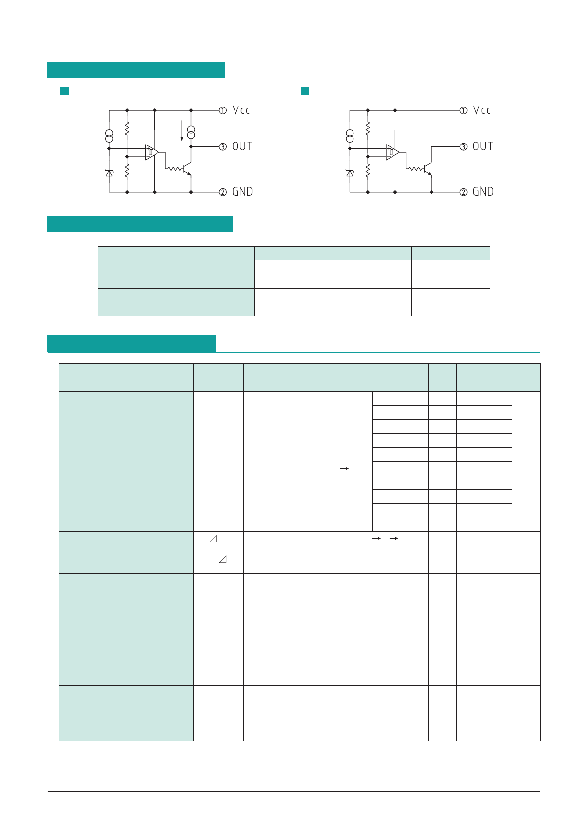
7. Output form
PST993 : Constant current load built-in
PST994 : Open collector
CCH=300µA typ. ICCL=250µA typ.
D : 4.2V I : 2.9V
E : 3.9V J : 2.7V
F : 3.6V K : 2.5V
G : 3.3V L : 2.3V
(Same ranks for PST994 too)
Packages
TO-92A (PST993 , PST994 )
contains detection voltage rank.
*
Applications
1. Reset circuits for microcomputers, CPU and MPU.
2. Reset circuit for logic circuitry.
3. Level detecting circuit.
Pin Assignment
1 VCC
2 GND
3 V
OUT
MITSUMI
Equivalent Circuit Diagram
PST993 PST994
System Reset PST993, 994
Absolute Maximum Ratings
(Ta=25°C)
Item Symbol Ratings Units
Storage temperature T
Operating temperature T
Supply voltage V
STG
OPR
CC
-
40~+125
-
20~+75
-
0.3~10 V
Allowable loss Pd 300 mW
Electrical Characteristics
Item Symbol
(Ta=25
°
C) (The unit of resistance is Ω unless otherwise indicated.)
Measurement
Circuit
Measurement conditions Min. Typ. Max. Units
PST993C 4.27 4.5 4.73
PST993D 4.00 4.2 4.40
PST993E 3.70 3.9 4.10
PST993F 3.42 3.6 3.78
L=∞ PST993G 3.13 3.3 3.47
Detection Voltage V
S 1
R
V
CC=H L PST993H 2.94 3.1 3.26
PST993I 2.75 2.9 3.05
PST993J 2.56 2.7 2.84
PST993K 2.37 2.5 2.63
PST993L 2.18 2.3 2.42
Hysteresis Voltage V
Detection Voltage
Temperature Coefficient
Low Level Output Voltage V
Output Constant Current I
Circuit Current at ON Time I
Circuit Current at OFF Time I
"H" Transmission Delay Time
"L" Transmission Delay Time
Operating Threshold Voltage V
Output Current at ON Time 1
Output Current at ON Time 2 I
Do not apply onto the OUT terminal any voltage higher than that at the VCC terminal.
*
(
1) The tpLH is a function of the charging time of CL by output constant current.
*
The delay time of this IC is about 1 µS.
S 1RL=∞, VCC=L H L 30 50 100 mV
S/ T 1 RL=∞, Ta=
V
OL 1VCC=Vs min.
OC1VO=2.5V, VCC=5V, RL=∞
CCL 1VCC=Vs min.
CCH 1VCC=Vs typ. /0.85V, RL=∞ 300 500 µA
-
20~+75°C ±0.01 %/°C
-
0.05V, RL=1k 0.1 0.4 V
-
0.05V, RL=∞ 250 400 µA
tpLH 2 CL=100pF
tpHL 2 CL=100pF 1 µS
OPL1 RL=4.7k, VOL
R
I
OL1 1
OL2 1
VO=0.4V, VCC=Vs min. -0.05V
L=∞, VO=0.4V
V
CC=VS min.
-
20~+75
Ta=
<
0.4V 0.65 0.85 V
=
-
0.05V
°
C, RL=∞
°
C
°
C
V
-
40-25-17 µA
*
20
1
µS
615 mA
4mA
 Loading...