

MITSMI MM3105A, MM3104G, MM3104H, MM3104J, MM3104K Datasheet
...
MITSUMI
Low-Ripple, Low-Saturation CMOS Regulators MM309X/MM310X Series
Low-Ripple, Low-Saturation CMOS Regulators
Monolithic IC MM309X, MM310X Series
Outline
This is a voltage regulator IC developed using the CMOS process.
Use of the CMOS process allows low current consumption, and it has superior ripple rejection ratio and
transient response compared to conventional CMOS process regulator ICs, making it ideal for use in portable
communications devices.
Ceramic capacitors can be used for the output capacitors.
Ideal for small, portable devices as SOT-25 and WLCSP are used for the package.
Features
1. Super low consumption current
45µA typ. (when not loaded, excluding the CE terminal current)
2. Super low consumption current (when off) 0.1µA typ.
3. High precision output voltage ±2%
4. Output current 150mA
5. Input/output voltage difference 0.23V typ. (Io=100mA, 3V output)
6. High ripple rejection ratio 80dB typ.
7. Built-in short-circuit restriction circuit 30mA typ.
8. Wide operating temperature range
-
30~+85°C
9. Output voltage 1.8~5.0V (0.1V step)
Applications
1. Constant voltage power supply for devices that use batteries
2. Constant voltage power supply for portable communications devices
3. Constant voltage power supply for household electronics products
Package
SOT-25, WLCSP-4 (MM309X),
WLCSP-5 (MM310X)
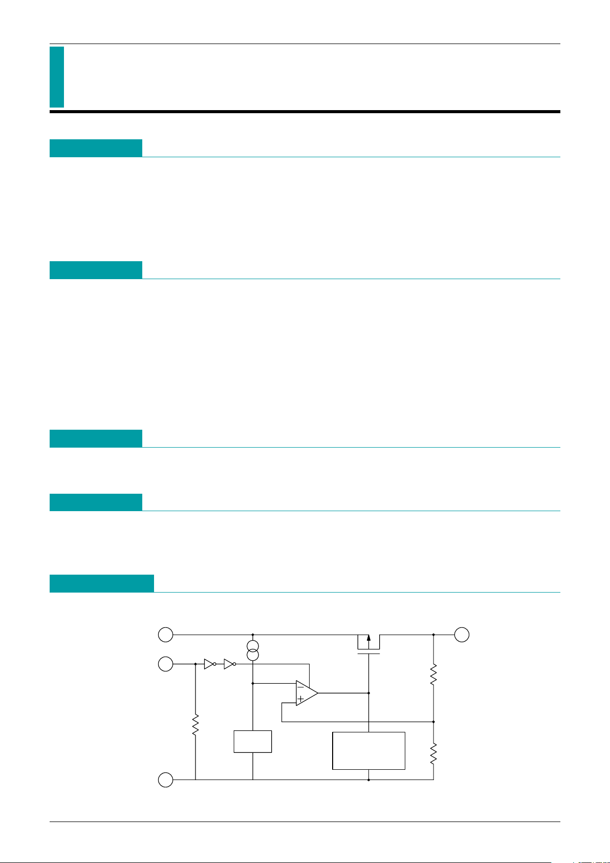
Block Diagram
V
GND
1
VDD
3
Current
Limit
REF
OUTV
2
CE
4
MITSUMI
Low-Ripple, Low-Saturation CMOS Regulators MM309X/MM310X Series
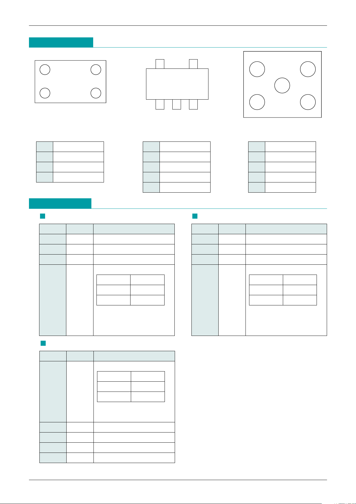
Pin Assignment
Pin Description
Pin No. Pin name
Functions
1 GND GND pin
2 V
OUT
Regulator output pin
3 VDD Voltage-supply pin
ON/OFF-Control pin
4 CE
Connect CE pin with V
DD
pin, when it is not used.
CE OUTPUT
L OFF
HON
4
1
3
2
WLCSP-4
(BOTTOM VIEW)
1 GND
2 V
OUT
3 VDD
4 CE
54
123
SOT-25A
(TOP VIEW)
1 VOUT
2 GND
3 V
DD
4 CE
5 V
DD
4
2
3
5
1
WLCSP-5
(BOTTOM VIEW)
1 CE
2 GND
3 V
OUT
4 VDD
5 NC
WLCSP-4
Pin No. Pin name
Functions
1 V
OUT
Regulator output pin
2 GND GND pin
3,5 V
DD Voltage-supply pin
ON/OFF-Control pin
4 CE
Connect CE pin with V
DD
pin, when it is not used.
CE OUTPUT
L OFF
HON
SOT-25A
Pin No. Pin name
Functions
ON/OFF-Control pin
1 CE
Connect CE pin with V
DD
pin, when it is not used.
2 GND GND pin
3 V
OUT
Regulator output pin
4 V
DD Voltage-supply pin
5 NC
CE OUTPUT
L OFF
HON
WLCSP-5
MITSUMI
Low-Ripple, Low-Saturation CMOS Regulators MM309X/MM310X Series
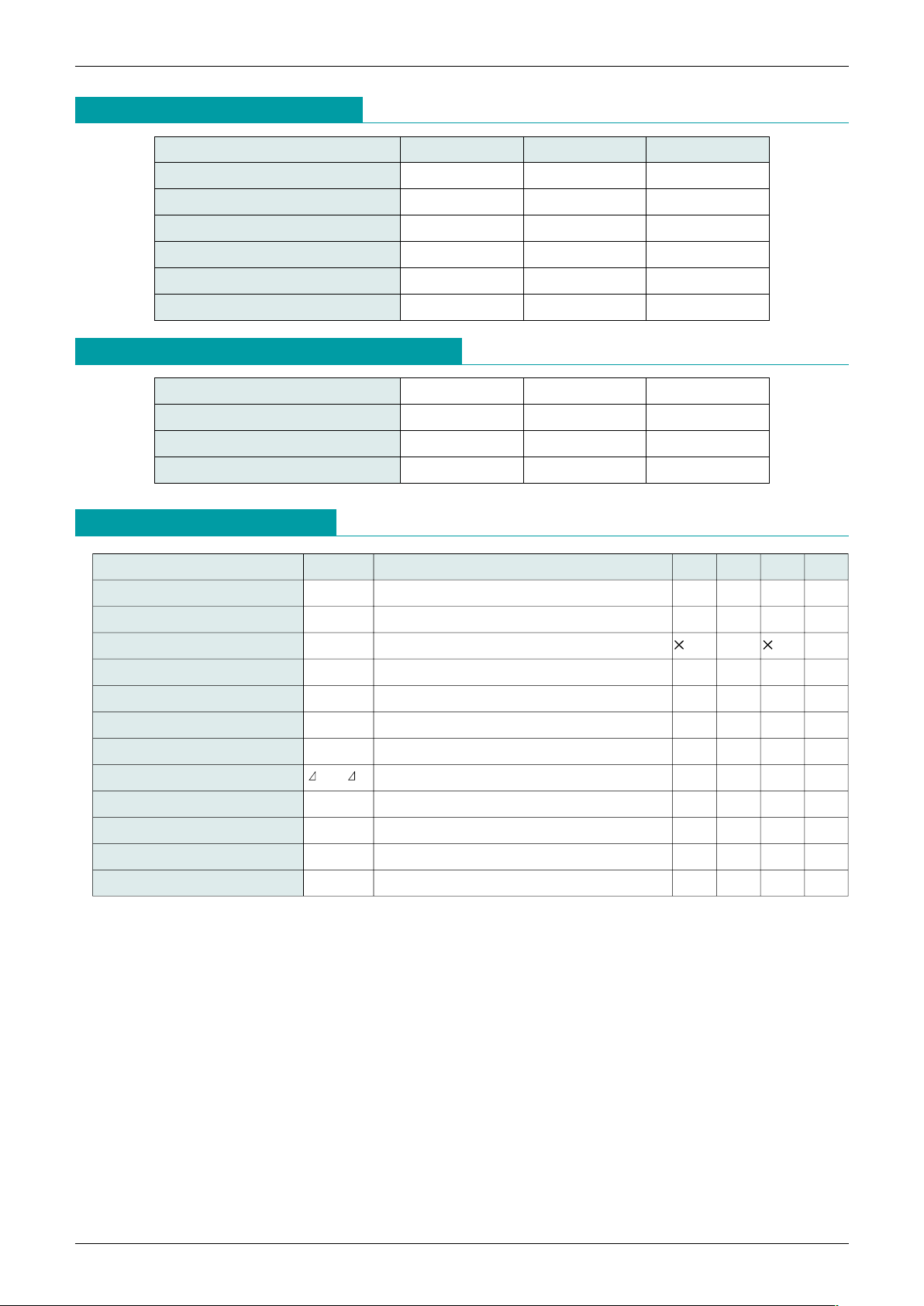
Electrical Characteristics
(VDD=VOUT typ.+1V, VCE=VDD, Ta=25°C
unless otherwise speciffied
)
Item Symbol Measurement conditions Min. Typ. Max. Unit
Input Current(OFF) I
DDOff VCE=0V 0.1 1.0 µA
No-Load Input Current I
DD 45 100 µA
Output Voltage V
OUT 1mA
<
=
I
OUT
<
=
30mA 0.98 1.02 V
Line Regulation V
LINE VDD=VO typ.+0.5~6V IOUT=30mA 0.05 0.20
%/V
Load Regulation VLOAD 1mA
<
=
I
OUT
<
=
80mA 20 45 mV
Dropout Voltage Vio Please refer to another page V
Ripple Rejection
*
1 RR Please refer to another page dB
V
OUT
Temperature Coefficient *1
V
OUT
/ T
IOUT=10mA -40mA
<
=
T
OPT
<
=
85°C ±100
ppm/°C
Output Short-Circuit Current *1 Ilim VO=0V 30 mA
CE Pull-down Resistance R
pd 2.5 5 15 MΩ
CE High Threshold voltage V
CEH 1.5 VDD V
CE Low Threshold voltage V
CEL 0 0.25 V
Absolute Maximum Ratings
(Ambient Temperature, Ta=25°C)
Item Symbol Ratings Unit
Storage Temperature T
STG
-
55~+125 °C
Supply Voltage V
DD 7V
CE Input Voltage V
OUT
-
0.3~VDD+0.3 V
Output Voltage V
OUT
-
0.3~VDD+0.3 V
Output Current I
Omax. 200 mA
Power Dissipation Pd 190 mW
Recommended Operating Conditions
(Ambient Temperature, Ta=25°C)
Item Symbol Ratings Unit
Operating Temperature T
jop
-
40~85 °C
Operating Voltage V
OP 2~6 V
Output Current I
O 0~150 mA
Note: *1 design guaranteed.
 Loading...