

MITSMI MM1210XF Datasheet

MITSUMI
Remaining Battery Power Display MM1210
Remaining Battery Power Display
Monolithic IC MM1210 Series
Outline
This IC detects battery voltage and displays the remaining power in the battery using an LCD. Long life and
light weight are emphasized in the most recent portable equipment, which increasingly use nickel cadmium
and nickel hydrogen batteries. For these batteries, the discharge characteristics mean that extremely precise
detection of the remaining battery power is required.
This IC enables detection of this type through high precision voltage detection.
Features
1. Two built-in detection voltages 1.18V / 1.06V typ.
2. High precision detection voltages ±1% typ.
3. Low current consumption During detection ; 15 µA typ.
During waiting ; 15 µA typ.
4. Setting possible during non-induction
It is possible to set a time period for which detection is ignored, as for example when voltage drops due to
temporary heavy loads.
5. Ripple absorption pins
It is possible to check fluctuations in detection through continuous rippling.
6. Built-in hysteresis voltage
Package
SOP-8D (MM1210XF)
Absolute Maximum Ratings
Item Rating
Storage temperature
-
40~+125°C
Operating temperature
-
20~+70°C
Input voltage 5V
Output pin voltage 5V
Allowable loss 300mW
MITSUMI
Remaining Battery Power Display MM1210
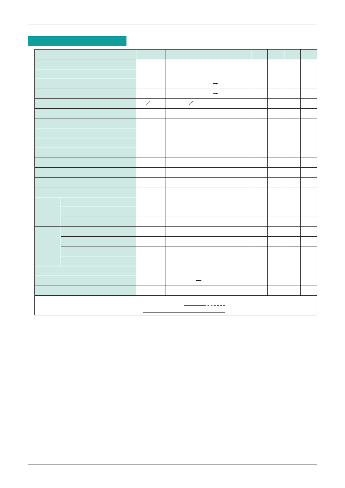
Electrical Characteristics
(Unless otherwise specified Ta=25°C, VCC=1.5V, VCE=VCC)
Item Symbol Measurement Conditions Min. Typ. Max. Unit
Current consumption I
CC1VCC=1.5V 15 25 µA
Current consumption during waiting I
CC2VCC=1.3V, VCE=0.3V 1.5 2.5 µA
Detection voltage IV
TH1VCC=H L 1.169 1.180 1.191 V
Detection voltage II V
TH2VCC=H L 1.050 1.060 1.070 V
Detection voltage Difference V
T VT=VTH1
-
VTH2 100 120 140 mV
Detection voltage temperature factor ±200
PPM/°C
Hysteresis voltage VHYS 10 20 35 mV
Output sink current II
S1VCC=1.3V, VO1=0.3V 40 µA
Output sink current II I
S2VCC=1.3V, V02=0.3V 40 µA
Output saturation voltage IV
O1ISINK=30UA 150 250 mV
Output saturation voltage II V
O2ISINK=30UA 150 250 mV
Output leak voltage II
LE1VCC=1.0V, VO1=0.5V 1 µA
Output leak voltage II I
LE2VCC=1.0V, VO2=1.5V 1 µA
Power supply voltage operating limit V
OPL VCC=variable, VO < 0.4V 0.70 0.75 V
Input H voltage V
CEH
-
0.3 VCC 0.3 V
Input L current I
CEH VCC=1.5V, VCE=0V 100 300 500 nA
Input L voltage V
CEL
-
0.3 0 0.3 V
Threshold value IV
THT VCC=1.0V, VTC=variable 0.34 0.42 0.50 V
Threshold value II V
THT VCC=1.0V, VTC=variable 0.04 0.12 0.20 V
Discharge current I
DIS VCC=1.0V, VTC=0.5V 30 60 90 nA
Charge current I
CHA VCC=1.5V, VTC=0.5V 0.40 0.80 1.20 µA
Non-induction time td V
CC=1.5V, C=0.033UF 120 180 240 mS
L transmission delay time tdLH V
CC=L H, C=0.033UF 1.0 2.0 4.0 mS
Ripple absorption resistance RRIP
measure resistance between pins8-
6 70 100 130 kΩ
CE pin
TC pin
Note : VCC applied pulse conditions
td1 td2
1.25V 1.15V
GND 1.10V 1.00V
V
CC applied pulse
 Loading...