

MITSMI MM1181ZM, MM1181ZT, MM1180IT, MM1180JM, MM1180JT Datasheet
...
MITSUMI
Low-Noise, Low-Satulation Three-Pin Regulator MM1180, 1181
Low-Noise, Low-Satulation Three-Pin Regulator
Monolithic IC MM1180, 1181
Outline
MM1180 series is high withstand voltage, low noise stabilized power supply with reduced reactive current at
low input voltage and small input / output differential voltage 0.2V at 40mA output current. The output current
is up to 100mA. MMP-4P package can control output ON / OFF by ON / OFF terminal.
Features
1. Input voltage 16V max.
2. Input / output differential voltage 0.2V typ. (Io=40mA)
3. Output noise voltage 100µV
RMS typ.
4. Maximum output current 100mA max.
5. No-load input current 300µA typ.
6. With thermal shutdown circuit
7. Output rank G : 5.0V±4% J : 3.0V±4%
I : 4.0V±4% Z : 3.3V±4%
H : 4.5V±4% C : 4.8V±4% (MM1181)
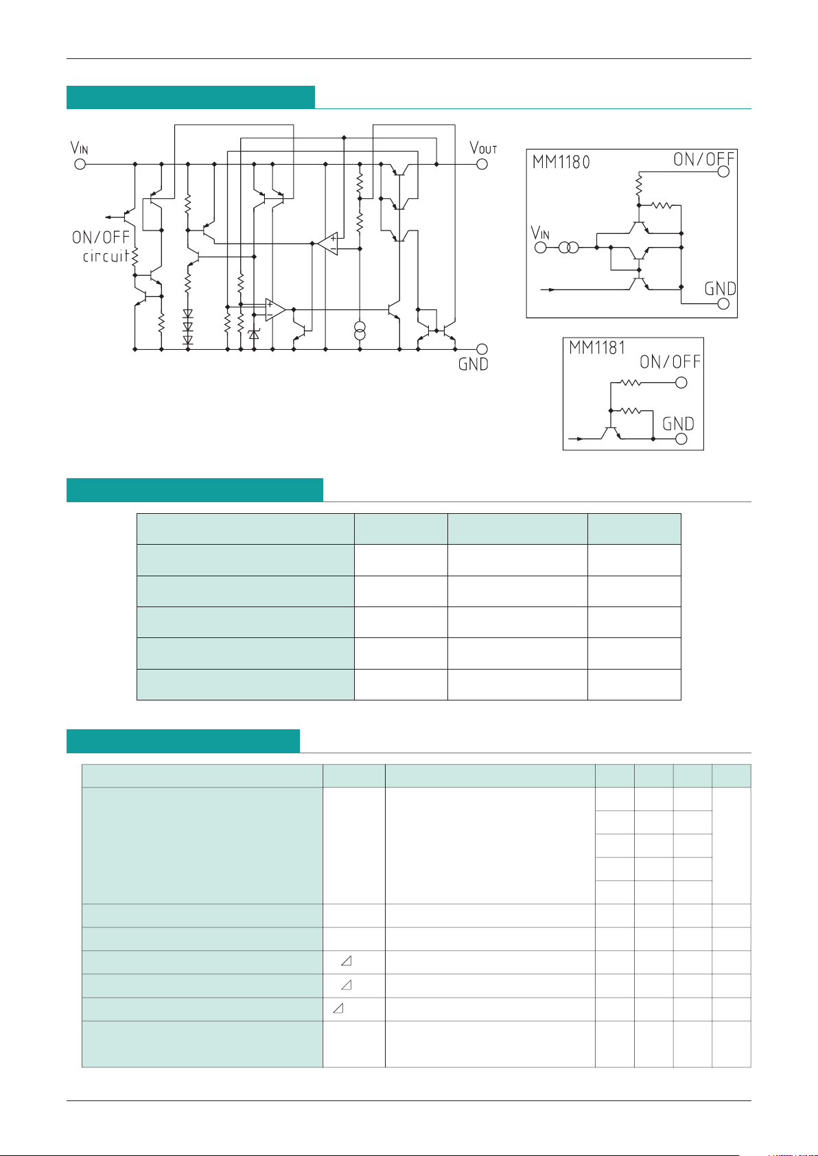
8. Output ON / OFF control function
(MMP-4A only)
On/Off Pin Level Low High
MM1180 output ON OFF
MM1181 output OFF ON
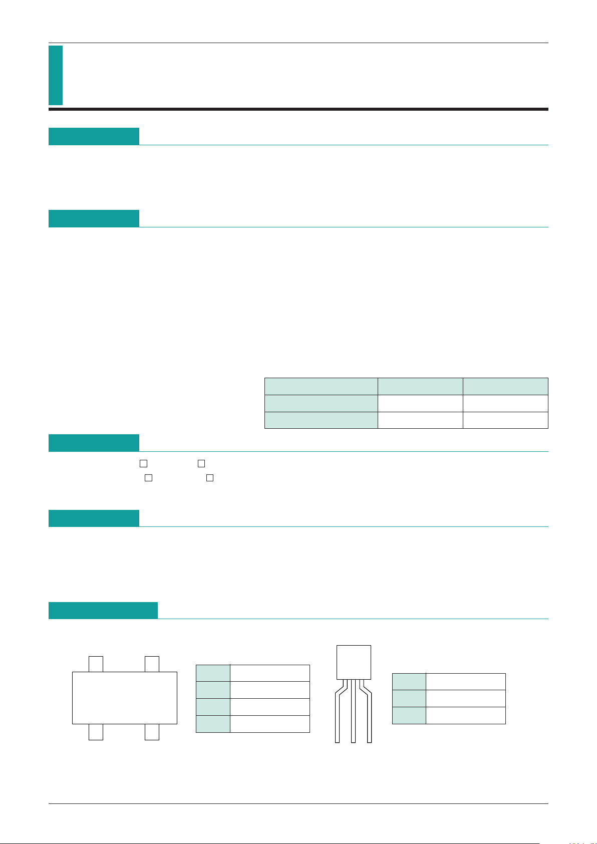
Package
TO-92A (MM1180 T, MM1181 T)
MMP-4A (MM1180 M, MM1181 M)
*
The output voltage rank appears in the boxes.
Applications
1. Handheld computers
2. Handy transceivers
3. Cordless phones
4. Portable equipment with battery
1 VOUT
2 VIN
3
ON/OFF terminal
4 GND
1 VIN
2 GND
3 V
OUT
12
43
MMP-4A
123
TO-92A
Pin Assignment
MITSUMI
Low-Noise, Low-Satulation Three-Pin Regulator MM1180, 1181
Equivalent Circuit Diagram
ON/OFF circuit
Absolute Maximum Ratings
Item Symbol Rating Unit
Storage temperature T
STG
-
40~+125 °C
Operating temperature T
OPR
-
20~+75 °C
Supply voltage V
CC max.
-
0.3~16 V
Output current I
OUT 100 mA
Allowable loss Pd
200 (MMP-4A), 300 (T0-92A)
mW
Electrical Characteristics
(Ta=25°C)
Item Symbol Measurement conditions Min. Typ. Max. Units
4.80 5.00 5.20
4.32 4.50 4.68
Output voltage Vo
V
IN=Vo+1V
3.84 4.00 4.16 V
Io=40mA
2.88 3.00 3.12
3.17 3.30 3.43
No-load input current Iccq V
IN=Vo+1V, Io=0µA 300 450 µA
Min Input / output differential voltage
Vd min. VIN=Vo min., Io=40mA 0.2 0.3 V
Line regulation V2 V
IN=(Vo+1V)~16V, Io=40mA
±0.01 ±0.1
%/V
Load regulation V1 V
IN=Vo+1V, Io=0~100mA
±0.01 ±0.03
%/mA
Output voltage temperature coefficient
Vo/T Ta=-20~+75°C ±100
ppm/°C
Ripple rejection rate RR
V
IN=Vo+2V, f=120Hz, Io=40mA
50 60 dB
V
RIPPLE=1V
 Loading...