

MITSMI MM1145BF, MM1145AF Datasheet

MITSUMI
System Reset (with built-in watchdog timer) MM1145
System Reset (with built-in watchdog timer)
Monolithic IC MM1145
Outline
This IC has a built-in watchdog timer, with 2 channels for a clock monitoring function that monitors the
microcomputer and outputs an intermittent reset signal if the microcomputer runs wild. Also, it has a power
supply voltage monitoring function (system reset function) which generates a reset signal if power supply
voltage is momentarily interrupted or drops, and performs power ON reset during normal power supply
recovery and when power is turned on.
Features
1. Built-in edge trigger input watchdog timer
2. 2 clock pulse monitoring
3. Power ON reset time (T
PR) and watchdog timer monitoring time (TWD) can be set individually with external
elements (R, C)
4. Excellent watchdog timer monitoring time (T
WD) precision A type : ±20%
B type : ±30%
5. Watchdog function stop pin allows use as system reset IC
6. Accurate power supply voltage drop detection 4.2V±3.5%
7. Detection voltage has hysteresis 100mV typ. ±0.14%/°C
8. Low reset minimum voltage
9. Low current consumption 150µA typ.
Package
SOP-8C (MM1145AF, MM1145BF)
Applications
Voltage detection for CPUs, microcomputers, etc. and clock pulse monitoring
Series Table
Model VSL TPR TWA TWR
MM1145A
4.2
100mS 50mS 10mS
MM1145B 40mS 110mS 10mS
*
CT=0.02µF, RCT=1MΩ
V
SL : Reset detection voltage
T
PR :Reset hold time during Vcc rise
T
WD :Watchdog timer monitoring time
T
WR : Reset time
MITSUMI
System Reset (with built-in watchdog timer) MM1145
1432
8567
SOP-8C
Pin Assignment
Pin Description
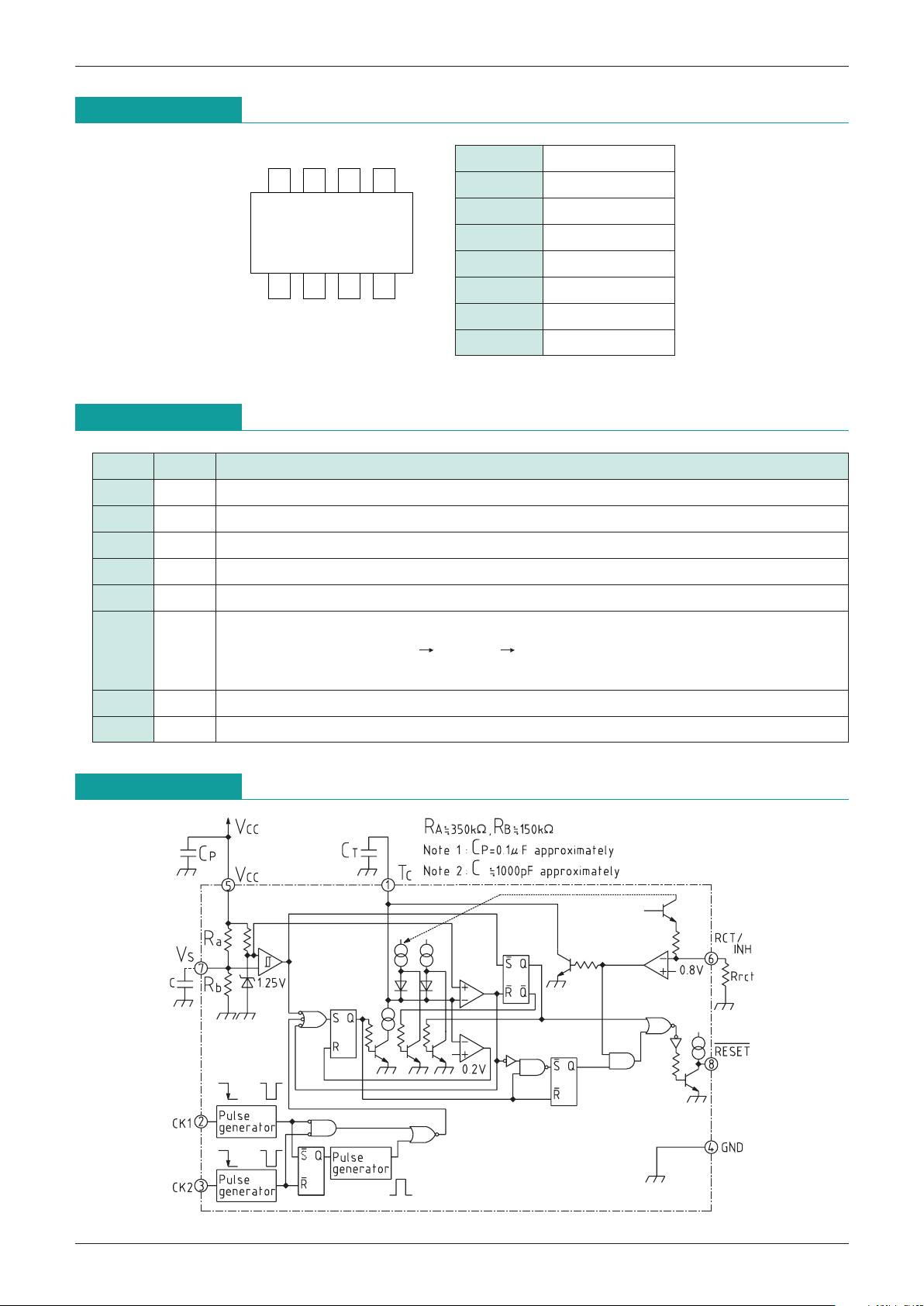
Block Diagram
1 TC
2 CK1
3 CK2
4 GND
5 V
CC
6 RCT
7 V
S
8 RESET
----------------------------------------------
Pin No.
Pin name
Function
1 TC
2 CK1
3 CK2
4 GND
5 V
CC
6 RCT
7 V
S
8 RESET
----------------------------------------------------------------------------------------------------------
TWD, TWR, TPR time setting pins. Time determined by external capacitor.
Clock input pin 1 Clock input from logic system
Clock input pin 2 Clock input from logic system
GND pin
Power supply pin Detection voltage 4.2V
Watchdog timer stop pin and T
WD adjustment pin
Operation modes : Operation Vcc, Stop GND
T
WD time determined by external resistor RRCT and CT
Detection voltage adjustment pin
Reset output pin (low output)

MITSUMI
System Reset (with built-in watchdog timer) MM1145
Absolute Maximum Ratings
Item Symbol Rating Units
Power supply voltage V
CC max.
-
0.3~+7.5 V
CK pin input voltage V
CK
-
0.3~VCC+0.3 (
<
=
+7.5) V
VS pin input voltage V
VS
-
0.3~VCC+0.3 (
<
=
+7.5) V
Voltage applied to RCT pin V
RCT
-
0.3~VCC+0.3 (
<
=
+7.5) V
Voltage applied to RESET
----------------------------------------------
pin VOH
-
0.3~VCC+0.3 (
<
=
+7.5) V
Allowable loss Pd 300 mW
Storage temperature T
STG
-
40~+125
°
C
Recommended Operating Conditions
Item Symbol Rating Units
Power supply voltage V
CC +2.2~+7.0 V
RESET sync current
I
OL 0~4.0 mA
Clock monitoring time setting T
WD 1.95~10000 mS
Power supply voltage rise and fall times
tFV, tRV <300 µS
Clock rise and fall times t
FC, tRC <100 µS
C
T pin capacitance CT 0.002~2 µF
RCT pin resistance Rr
CT 0.39~2 MΩ
Operating temperature T
OP
-
25~+75
°
C
Item Symbol Measurement conditions Min. Typ. Max. Units
Consumption current I
CC During watchdog timer operation 150 180 µA
Detection voltage
V
SL 4.05 4.20 4.35
V
V
SH 4.15 4.30 4.45
Detection voltage
±0.01 %/
°
C
temperature coefficient
Hysteresis voltage V
HYS 50 100 150 mV
CK input threshold V
TH 0.8 1.2 2 V
CK input current
I
IH VCK=5.0V 0 1
µA
I
IL VCK=0V
-
14.5-8.5
-
4.5
Output voltage (High) V
OH I=
-
1µA, VS=OPEN 4.0 4.5 V
Output voltage (Low)
V
OL1 I =0.5mA, VS=0V 0.10 0.20
V
V
OL2 I =2.0mA, VS=0V 0.15 0.35
Output sync current I
OL V =1.0V, VS=0V 2 4 mA
MM1145A
I
CT1 During watchdog timer operation
-
0.40-0.48-0.60
µA
C
T charge MM1145B
-
0.17-0.22-0.30
current MM1145A
I
CT2 During power ON reset operation
-
0.21-0.31-0.62
µA
MM1145B
-
0.62-0.93-2.33
Minimum operating power supply
VCCL 0.8 1.0 V
voltage to ensure RESET
-----------------------------------------------
RESET
--------------------------------------------
RESET
--------------------------------------------
RESET
--------------------------------------------
RESET
--------------------------------------------
VS=OPEN, VCC
VS=OPEN, VCC
VSH-VSL, VCC
V =0.4V
I =0.1mA
RESET
--------------------------------------------
RESET
--------------------------------------------
VS
T
Electrical Characteristics (DC)
(Except where noted otherwise, Ta=25°C, Vcc=5.0V)
 Loading...