

MITSMI MM1130XD Datasheet
MITSUMI
NTSC PAL Converter MM1130
NTSC PAL Converter
Monolithic IC MM1130
Outline
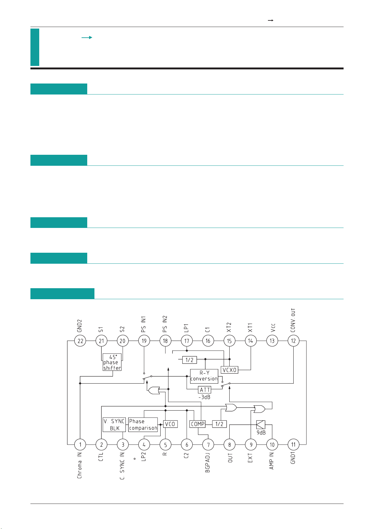
This is an NTSC/PAL signal switching IC.
In PAL conversion mode, a frequency-converted (fc=4.43MHz) NTSC format chroma signal is phase
converted (R-Y axis component is inverted) every 1 hour by shifting burst signal phase by 45°.
Circuit configuration includes VCO (horizontal sync), VCXO (phase conversion carrier), phase conversion
circuit, switches, amps, etc.
Features
1. PAL conversion with phase conversion performed
2. Two possible phase conversion carriers : crystal oscillation and external input
3. No adjustments
4. Four possible mode selections by CTL and EXT pins
Package
SDIP-22A (MM1130XD)
Applications
1. VCR
Block Diagram

MITSUMI
NTSC PAL Converter MM1130
Pin Description
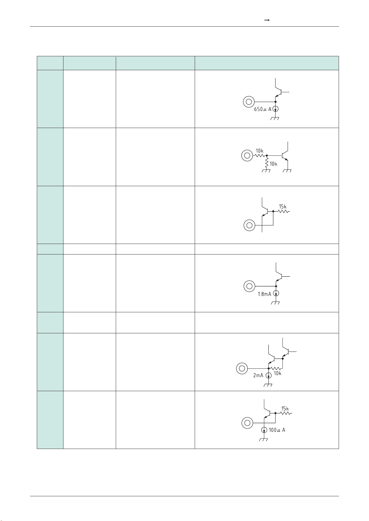
Pin no. Pin name Function Internal equivalent circuit diagram
1 chroma IN Inputs chroma signal
2 CTL Mode setting pin
3 C.SYNC IN Inputs composite sync
signal
4 LP2 Time constant connection
pin for H. SYNC APC loop
LPF
5 R H. SYNC APC feedback pin
6 C2 Pin for connecting H.
SYNC APC free run
frequency setting capacitor
7 BGP ADJ Fine tuning of position for
sampling burst signal. Use
open.
MITSUMI
NTSC PAL Converter MM1130
Pin no. Pin name Function Internal equivalent circuit diagram
8 OUT Amp output pin
9 EXT Mode setting pin
10 AMP IN Amp input pin
11 GND1 GND pin
12 CONV.OUT Multiplication circuit output
pin
13 VCC VCC pin.
Inputs 5V.
14 XT1 Carrier (2fsc) oscillation
circuit output pin
15 XT2 Carrier (2fsc) input pin
 Loading...