MITEL MH88422-1, MH88422BD-1, MH88422-2, MH88422-3 Datasheet

MH88422
Data Access Arrangement
Preliminary Information
Features
• FAX and Modem interface (V29)
• Variants available with different line
impedances
• Provides reinforced barrier to international PTT
requirements
• Transformerless 2-4 Wire conversion.
• Integral Loop Switch
• Dial Pulse and DTMF operation
• Line state detection outputs
• Loop current/ringing outputs
• Single +5V operation, low on-hook power
(5mW)
• Full duplex data transmission
Applications
Interface to Central Office or PABX line for:
• Modem
•FAX
• Telemetr y
DS5067 ISSUE 10 November 1998
Ordering Informations
MH88422-1/2/3 26 Pin DIL Package
MH88422BD-1 26 Pin DIL Package
0°C to 70°C
Description
The Mitel MH88422 Data Access Arrangement
(D.A.A.) provides a complete interface between data
transmission equipment and a telephone line. All
functions are integrated into a single thick film hybrid
module which provides high voltage isolation, very
high reliability and optimum circuit design needing a
minimum of external components.
A number of variants are available to meet particular
country impedance requirements. The D.A.A. has
been designed to meet regulatory approvals
requirements in these countries.
TIP
RING
TXIN
TF
RLS
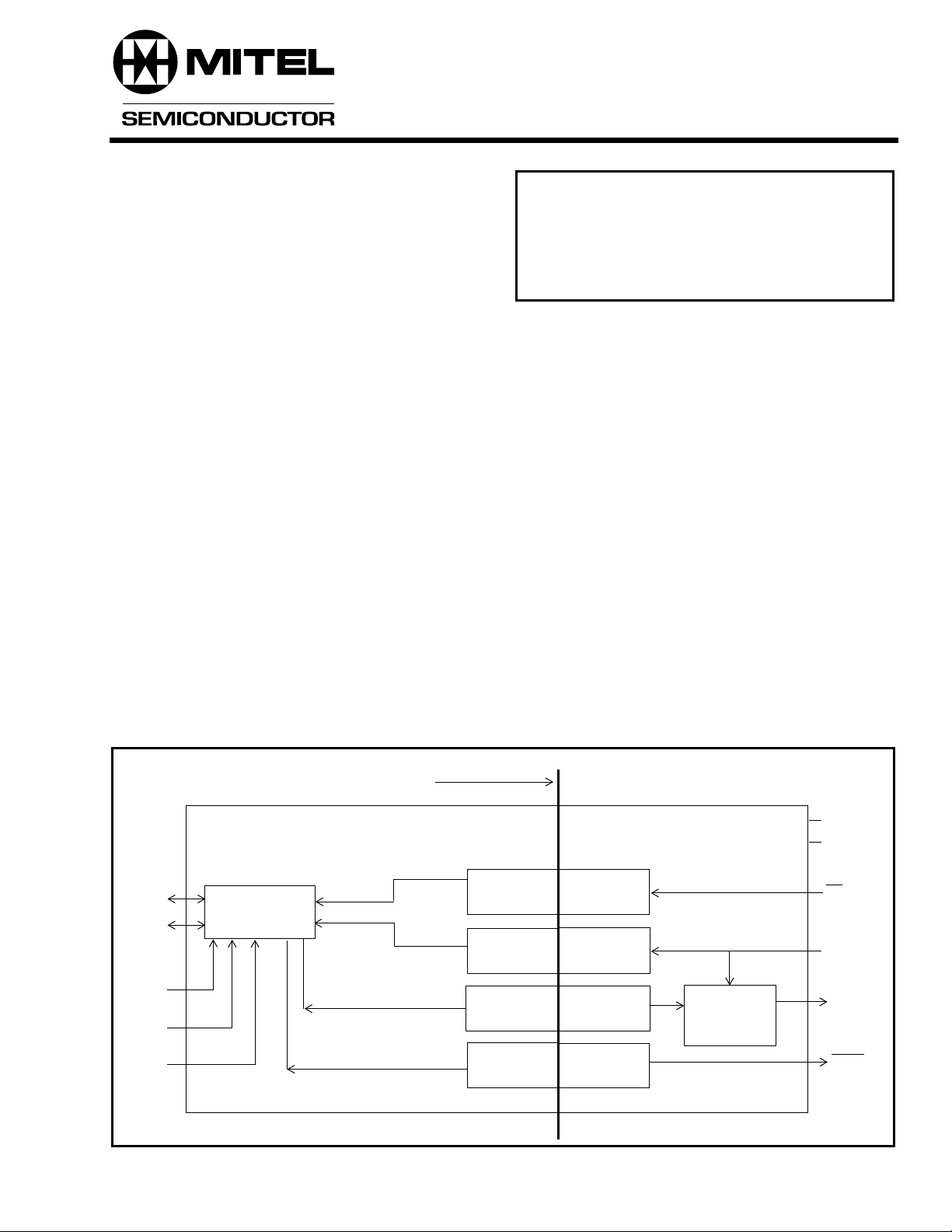
Input Buffer
&
Line Termination
Network Connections
Isolation Barrier
Opto-
Isolation
Opto-
Isolation
Opto-
Isolation
Opto-
Isolation
Logic Input
Buffer
Audio
Buffer
Audio
Buffer
Ring & Loop
Buffer
User Connections
Figure 1 - Functional Block Diagram
Transhybrid
loss
cancellation
circuit
VDD
AGND
LC
VR
VX
RVLC
2-13

MH88422 Preliminary Information
VDD
IC
AGND
IC
LC
IC
RVLC
IC
IC
IC/NP
VX
IC/NP
VR
1
2
3
4
5
6
7
8
9
10
11
12
13
26
25
24
23
22
21
20
19
18
17
16
15
14
TIP
IC
RLS
IC/NP
IC
IC/NP
TF
NP
TXIN
IC
RING
NP
IC
Figure 2 - Pin Connections
Pin Description
Pin # Name Description
1 VDD Positive Supply Voltage. +5V.
2, 4, 6,
8, 9
3 AGND Analog Ground. 4-Wire Ground. Normally connected to System Ground.
5 LC Loop Control (Input). A logic 0 activates internal circuitry which provides a line
IC Internal Connection. This pin is cropped short.
termination across Tip and Ring. Used for seizing the line and dial pulsing.
7 RVLC Ringing Voltage and Current Detect (Output). Indicates the status of loop current
and ringing voltage.
10, 12 IC/NP Internal Connection or No Pin Fitted. This pin is either cropped shor t or not fitted,
depending on the variant. See Note 1
11 VX Transmit (Output). Analog output to modem/fax chip set.
13 VR Receive (Input). Analog input to modem/fax chip set.
14, 17 IC Internal Connection. This pin is cropped short.
15, 19 NP No Pin Fitted.
16 RING Ring Lead. Connects to the "Ring" lead of a telephone line.
18 TXIN Dummy Ringer Connection. Connects to the "Ring" lead of a telephone line through a
dummy ringer capacitor.
20 TF Tip Feed. Connects externally to the RLS pin.
21, 23 IC/NP Internal Connection or No Pin Fitted. This pin is either cropped shor t or not fitted,
depending on the variant. See Note 1
24 RLS Ringing Loop Sense. Connects externally to the TF pin.
25 IC Internal Connection. This pin is cropped short.
26 TIP Tip Lead. Connects to the "Tip" lead of a telephone line.
Notes:
1. Variant 1, 4 BD-1 - pins 10,12, & 21 are cropped short. Pin 23 is not fitted.
2. Variant 2 - pin 23 is cropped short. Pins 10, 12 & 21 are not fitted.
3. Variant 3 - pins 12 and 21 are cropped short. Pins 10 and 23 are not fitted.
2-14

Preliminary Information MH88422
Functional Description
The device is a Data Access Arrangement (D.A.A.). It
is used to correctly terminate a 2-Wire analog loop. It
provides a signalling link and a 2-4 Wire line
interface between an analog loop and the
subscriber’s data transmission equipment such as
Modems, Facsimiles (Fax’s), Remote Metering and
Electronic Point of Sale equipment (EPOS).
Isolation Barrier
The device provides an isolation barrier implemented
by using optocouplers. This is a reinforced barrier for
an instantaneous power surge of up to 3kV r.m.s., for
example a lightning strike. It also provides full
isolation for a continuous AC voltage level of up to
250V r.m.s.
External Protection Circuit
Should the input voltage from the line exceed that
isolated by the optocoupler, an External Protection
Circuit assists in preventing damage to the device
and the subscriber equipment. See Figure 3.
Input Impedance
The MH88422 is available in a number of different
variants each of which has its own fixed Tip-Ring AC
input impedance (Zin). Each variant is identified by
the final digit in its part number, as listed below. Also
shown are the countries whose PTT requirements
match these impedances.
MH88422-1 Zin = 220Ω + 820Ω // 120nF
Australia / South Africa / Spain
MH88422BD-1 Zin = 220Ω + 820Ω // 115nF
German BABT ZV5
MH88422-2 Zin = 600Ω
North America
MH88422-3 Zin = 370Ω + 620Ω // 310nF
UK / New Zealand
Many of these countries now pass equipment
approved to CTR21. The MH88422 will not meet this
specification. See the MH88437 datasheet for a
CTR21 Product.
Line Termination
When Loop Control (LC) is at a logic 0, a line
termination is applied across Tip and Ring. The
device can be considered off-hook and DC loop
current will flow. The line termination consists of both
a DC line termination and an AC input impedance.
When LC is at a logic 1, a Dummy Ringer is applied
across Tip and Ring. The device can be considered
on-hook and negligible DC current will flow. The
dummy ringer is an AC load, which represents a
telephone’s mechanical ringer.
DC Line Termination
When LC is at a logic 0, an active termination is
applied across Tip and Ring, at which time it can be
considered to be in an off-hook state. This is used to
terminate an incoming call, seize the line for an
outgoing call, or if it is applied and disconnected at
the required rate, can be used to generate dial
pulses. This termination resembles approximately
300Ω resistance, which is loop current dependent.
Dummy Ringer
This device supports a dummy ringer option which
can be configured by the inclusion of external
components. Further details relating to component
values and configuration can be obtained from
MSAN-154. For example, Figure 3 shows capacitor
C2 which if set to 1.8µF would meet the New
Zealand dummy ringer requirements.
2-4 Wire Conversion
The device converts the balanced 2-Wire input,
presented by the line at Tip and Ring, to a ground
referenced signal at VX, as required by modem/fax
chip sets.
Conversely the device converts the ground
referenced signal input at VR, to a balanced 2-Wire
signal across Tip and Ring.
During full duplex transmission, the signal at Tip and
Ring consists of both the signal from the device to
the line and the signal from the line to the device.
The signal input at VR, being sent to the line, must
not appear at the output VX. In order to prevent this,
2-15

MH88422 Preliminary Information
the device has an internal cancellation circuit. The
measure of attenuation is Transhybrid Loss (THL).
The Transmit (VX) and Receive (VR) signals are
ground referenced (AGND), and biased to 2.5V. The
device must be in the off-hook condition for
transmission or reception to take place.
Transmit Gain
The Transmit Gain of the MH88422 is the gain from the
differential signal across Tip and Ring to the ground
referenced signal at VX. The internal Transmit Gain of
the device is fixed and depends on the variant as
shown in the AC Electrical Characteristics table. For
the correct gain, the Input Impedance of the MH88422
variant used, must match the specified line
impedance.
By adding an external potential divider to VX, it is
possible to reduce the overall gain in the application.
The output impedance of VX is approximately 10Ω and
the minimum resistance from VX to ground should be
2kΩ.
Characteristics table. For the correct gain, the Input
Impedance of the MH88422 variant used, must match
the specified line impedance.
The input impedance to ground of VR is 47kΩ and this
can be used with an external series resistor to form a
potential divider and reduce the overall gain in the
application.
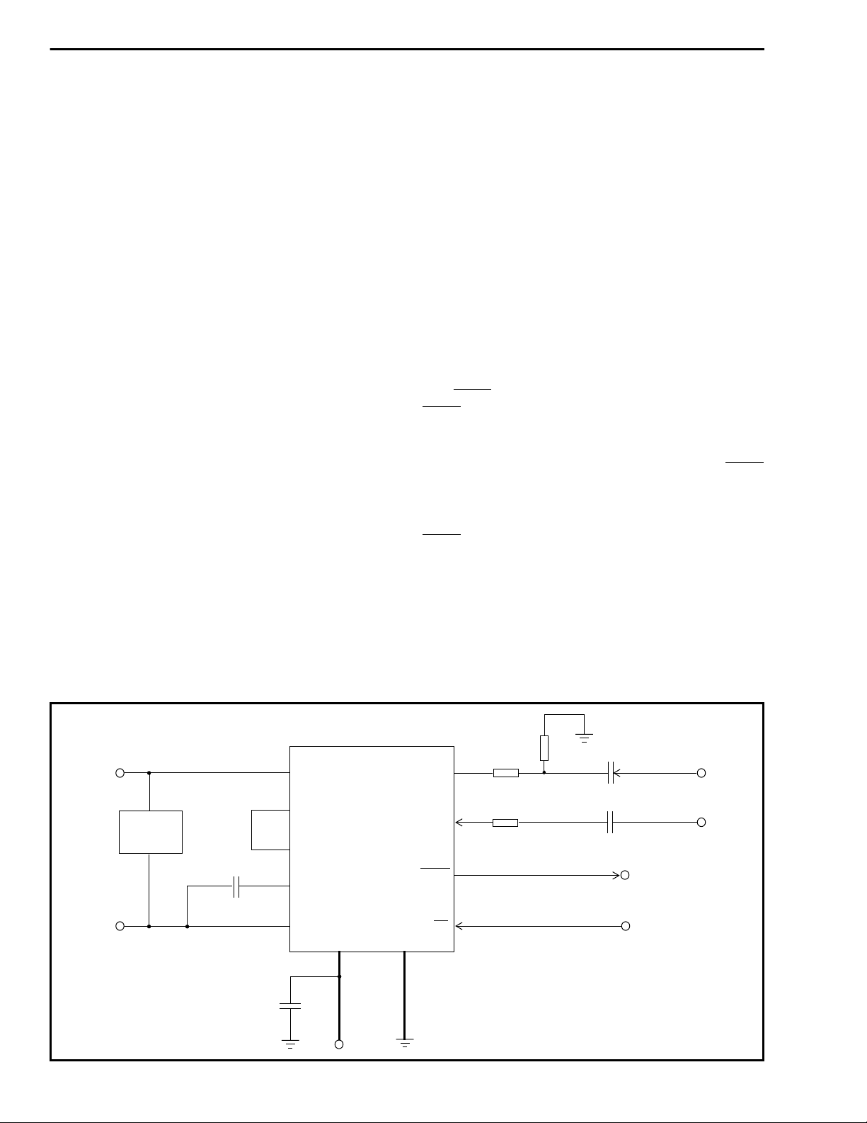
Example: If R3 = 100kΩ, in Figure 3, the Gain would
reduce by 3.0dB.
Supervisory Features
The device is capable of monitoring the line
conditions across Tip and Ring, this is shown in
Figure 3. The Ringing Voltage Loop Current detect
pin (RVLC), indicates the status of the device. The
RVLC output is at logic 0 when loop current flows,
indicating that the MH88422 is in an off hook state.
When the device is generating dial pulses, the RVLC
pin outputs a TTL pulse at the same rate.
Example: If R1 = R2 = 2kΩ, in Figure 3, the gain would
reduce by 6.0dB.
Receive Gain
The Receive Gain of the MH88422 is the gain from the
ground referenced signal at VR to the differential
signal across Tip and Ring. The internal Receive Gain
of the device is fixed as shown in the AC Electrical
MH88422
26
C1
24
20
18
16
TIP
RLS
TF
TXIN
RING
VDD
1
+
+5V
TIP
Protection
Circuit
C2
RING
Notes:
1) R1, R2: Transmit Gain Resistors
2) R3: Receive Gain Resistor
3) C1: 10µF 6V Tantalum
4) C2: Dummy Ringer Capacitor 250V
5) C3, C4: 10µF AC coupling Capacitors
An AC ringing voltage across Tip and Ring will cause
RVLC to output a TTL pulse at double the ringing
frequency with an envelope determined by the
ringing cadence.
Mechanical Data
See Figure 10, for details of the mechanical
specification.
R2
R1
AGND
3
VX
VR
RVLC
LC
11
13
7
5
R3
C3
C4
Ring Voltage & Loop
Current Detect Output
Loop Control Input
Audio
Output
Audio
Input
2-16
Figure 3 - Typical Application Circuit

Preliminary Information MH88422
Absolute Maximum Ratings* - All voltages are with respect to AGND unless otherwise specified.
Parameter Symbol Min Max Units
.
1 DC Supply Voltage V
2 Storage Temperature T
3 DC Loop Voltage V
4 Ringing Voltage - 2 variant
- all other variants
5 Loop Current I
*Exceeding these values may cause permanent damage. Functional operation under these conditions is not implied.
DD
S
BAT
V
R
V
R
Loop
-0.3 6 V
-55 +125 ˚C
-110 +110 V
-
-2
150
120
-90mA
Recommended Operating Conditions
Parameter Sym Min Typ‡Max Units Test Conditions
1 DC Supply Voltages V
2 Operating Temperatures T
3 Ringing Voltage V
‡ Typical figures are at 25˚C with nominal +5V supply and are for design aid only
Loop Electrical Characteristics
†
4.75 5.0 5.25
DD
OP
R
02570˚C
75 90 Vrms 150 Vrms for -2 variant
Characteristics Sym Min Typ‡Max Units Test Conditions
V
Vrms
Vrms
1 Ringing Voltage
-1 V ariant Only No Detect
Detect
BD-1 V ariant Only No Detect
Detect
All other V ariants No Detect
Detect
2 Ringing Frequency
BD-1 Variant Only
All other Variants
3 Operating Loop Current
BD-1 Variant Only
All other Variants
4 Off-Hook DC Voltage
-1 Variant
-2 Variant
-3 Variant
VR
35
32
14
23
15
20
15
6.0
2.4
3.1
6.0
17
15
7
28
68
80
80
28.8
6.0
6.0
7.8
9.0
14.0
Vrms
Vrms
Vrms
Vrms
Vrms
Vrms
Hz
Hz
mA
mA
V
V
V
V
V
V
V
Externally Adjustable See MSAN-154
Test circuit as Fig 4
I
=19mA (See Note 1)
Loop
I
=60mA
Loop
I
=15mA
Loop
I
=20mA (See Note 2)
Loop
I
=26mA
Loop
I
=15mA (See Note 3)
Loop
I
=90mA
Loop
BD-1 Variant
6.0
6.0
10.8
27
V
I
=20mA (See Note 4)
V
Loop
I
Loop
=50mA
2-17
 Loading...