

Page 1

Technical Information Manual
NetVista X40
Ty pe 6 6 4 3
Ty pe 2179
IBM
Page 2

Technical Information Manual
NetVista X40
Ty pe 6 6 4 3
Ty pe 2179
IBM
Page 3

Before using this information and the product it supports, be sure to read “Notices” on page 45.
Note
First Edition (May 2000)
© COPYRIGHT INTERNATIONA L BUSINESS MACHINES CORPORATION, 2000. All rights reserved.
Note to U.S. Government Users — Documentation related to restricted rights — Use, duplication or disclosure is subject
to restrictions se t forth in GSA ADP Schedule Contract with IBM Corp.
Page 4

IBM
Page 5

Contents
Preface . . . . . . . . . . . . . . . . . . . . . . . . . . . vii
Related publications . . . . . . . . . . . . . . . . . . . . . . . . . . . . . vii
Terminology usage . . . . . . . . . . . . . . . . . . . . . . . . . . . . . viii
Chapter 1.System Overview . . . . . . . . . . . . 1
Features. . . . . . . . . . . . . . . . . . . . . . . . . . . . . . . . . . . . . . . . . 1
DVD-ROM . . . . . . . . . . . . . . . . . . . . . . . . . . . . . . . . . . . . . . 2
ADSL modems. . . . . . . . . . . . . . . . . . . . . . . . . . . . . . . . . . . 2
Wake on LAN. . . . . . . . . . . . . . . . . . . . . . . . . . . . . . . . . . . . 2
Wake on Ring. . . . . . . . . . . . . . . . . . . . . . . . . . . . . . . . . . . . 2
Chapter 2.System board features . . . . . . . 3
Microprocessors. . . . . . . . . . . . . . . . . . . . . . . . . . . . . . . . . . 3
Intel Pentium III microprocessor with MMX
technology . . . . . . . . . . . . . . . . . . . . . . . . . . . . . . . . . . . . . . 3
Features . . . . . . . . . . . . . . . . . . . . . . . . . . . . . . . . . . . 3
L2 Cache. . . . . . . . . . . . . . . . . . . . . . . . . . . . . . . . . . . 3
Intel Celeron microprocessor . . . . . . . . . . . . . . . . . . . . 3
Features . . . . . . . . . . . . . . . . . . . . . . . . . . . . . . . . . . . 3
L2 Cache. . . . . . . . . . . . . . . . . . . . . . . . . . . . . . . . . . . 4
Chip set control . . . . . . . . . . . . . . . . . . . . . . . . . . . . . . . . . . 4
System memory . . . . . . . . . . . . . . . . . . . . . . . . . . . . . . . 4
PCI Bus . . . . . . . . . . . . . . . . . . . . . . . . . . . . . . . . . . . . . . 5
IDE bus master interface. . . . . . . . . . . . . . . . . . . . . . . . 5
USB interface . . . . . . . . . . . . . . . . . . . . . . . . . . . . . . . . . 5
Audio Subsystem . . . . . . . . . . . . . . . . . . . . . . . . . . . . . . . . 6
Integrated peripheral controller . . . . . . . . . . . . . . . . . . . . 6
Keyboard and mouse ports . . . . . . . . . . . . . . . . . . . . . 6
Network connection . . . . . . . . . . . . . . . . . . . . . . . . . . . . . . 7
Real-time clock and CMOS . . . . . . . . . . . . . . . . . . . . . . . . 7
Flash EEPROM . . . . . . . . . . . . . . . . . . . . . . . . . . . . . . . . . . 7
Expansion adapters. . . . . . . . . . . . . . . . . . . . . . . . . . . . . . . 7
System board . . . . . . . . . . . . . . . . . . . . . . . . . . . . . . . . . . . . 8
Cable connectors . . . . . . . . . . . . . . . . . . . . . . . . . . . . . . 8
POST . . . . . . . . . . . . . . . . . . . . . . . . . . . . . . . . . . . . . . . . . . 17
Configuration/Setup Utility program . . . . . . . . . . . . . . 17
Advanced Power Management (APM) . . . . . . . . . . . . . 18
Advanced Configuration and Power Interface (ACPI) 18
Flash update utility program. . . . . . . . . . . . . . . . . . . . . . 18
Diagnostic program. . . . . . . . . . . . . . . . . . . . . . . . . . . . . . 18
Chapter 6.System compatibility . . . . . . . . 19
Hardware compatibility . . . . . . . . . . . . . . . . . . . . . . . . . . 19
Hardware interrupts . . . . . . . . . . . . . . . . . . . . . . . . . . 19
Software compatibility . . . . . . . . . . . . . . . . . . . . . . . . . . . 20
Software interrupts . . . . . . . . . . . . . . . . . . . . . . . . . . . 20
Machine-sensitive programs. . . . . . . . . . . . . . . . . . . . 20
Appendix A. Connector pin assignments 21
System memory connector. . . . . . . . . . . . . . . . . . . . . . . . 21
PCI connectors. . . . . . . . . . . . . . . . . . . . . . . . . . . . . . . . . . 26
IDE connectors. . . . . . . . . . . . . . . . . . . . . . . . . . . . . . . . . . 28
Diskette drive connec tor. . . . . . . . . . . . . . . . . . . . . . . . . . 30
Power supply connector . . . . . . . . . . . . . . . . . . . . . . . . . . 31
Wake on LAN connectors. . . . . . . . . . . . . . . . . . . . . . . . . 31
Alert on LAN connector . . . . . . . . . . . . . . . . . . . . . . . . . . 31
USB port connectors . . . . . . . . . . . . . . . . . . . . . . . . . . . . . 31
Mouse and keyboard port connectors . . . . . . . . . . . . . . 32
Appendix B. System address maps. . . . . 33
System memory map . . . . . . . . . . . . . . . . . . . . . . . . . . . . 33
Input/output address map . . . . . . . . . . . . . . . . . . . . . . . 34
DMA I/O address map. . . . . . . . . . . . . . . . . . . . . . . . . . . 36
PCI configuration space map. . . . . . . . . . . . . . . . . . . . . . 37
Appendix C. IRQ and DMA channel
assignments. . . . . . . . . . . . . . . . . . . . . . . 39
Chapter 3.System specifications . . . . . . . 11
Chapter 4.Power supply . . . . . . . . . . . . . . 13
Power input . . . . . . . . . . . . . . . . . . . . . . . . . . . . . . . . . . . . 13
Power output. . . . . . . . . . . . . . . . . . . . . . . . . . . . . . . . . . . 13
Component outputs . . . . . . . . . . . . . . . . . . . . . . . . . . . . . 14
Output protection . . . . . . . . . . . . . . . . . . . . . . . . . . . . . . . 15
Connector description . . . . . . . . . . . . . . . . . . . . . . . . . . . 15
Chapter 5.System software. . . . . . . . . . . . 17
BIOS. . . . . . . . . . . . . . . . . . . . . . . . . . . . . . . . . . . . . . . . . . . 17
Plug and Play . . . . . . . . . . . . . . . . . . . . . . . . . . . . . . . . . . . 17
© Copyright IBM Corp. 2000 v
Appendix D. Error codes . . . . . . . . . . . . . 41
POST error c odes . . . . . . . . . . . . . . . . . . . . . . . . . . . . . . . . 41
Bibliography. . . . . . . . . . . . . . . . . . . . . . . . 43
Notices . . . . . . . . . . . . . . . . . . . . . . . . . . . . 45
Processing date data . . . . . . . . . . . . . . . . . . . . . . . . . . . . . 45
Trademarks. . . . . . . . . . . . . . . . . . . . . . . . . . . . . . . . . . . . . 46
Index . . . . . . . . . . . . . . . . . . . . . . . . . . . . . . 47
Page 6

vi Technical Info rm ation
Page 7

Preface
This Technical Information Manual provides information for your computer. This
publication is intended for developers who want to provide hardware and software
products to operate with your computer and provides an in-depth view of how the
computer works. Users of this publication should have an understanding of computer
architecture and programming concepts.
Related publications
In addition to this publication, the following IBM publications provide information
related to the operation of your computer. The publications mentioned here are
available from the IBM Web site. In some cases, you will have to follow further
instructions on the Web site to find the document for your particular computer and
model. To order printed publications, refer to the help information in the User Guide
that comes with your computer.
• User Guide
This publication contains information about configuring, operating, and
maintaining your computer, as well as installing new options. Also included are
warranty information, instructions f or diagnosing and solving problems, and
information on how to obtain help and service.
• About Your Software
This publication (provided only with computers that have IBM-preinstalled
software) contains information about the preinstalled s of tware, the Software
Selections CDs, and the Product Recovery CDs th at com e with your comput er.
• Hardware Maintenance Manual
This publication contains information for tra ined service technicians. It is
available at http://www.ibm.com/pc/support on the World Wide Web, and it
can also be ordered from IBM. To purchase a copy, see the help information in
the User Guide that comes with your computer.
© Copyright IBM Corp. 2000 vii
Page 8

Terminology usage
Attention: The term reserved describes certain signals, bits, and registers that should
not be changed. Use of reserved areas can cause compatibility problems, loss of data,
or permanent damage to the hardware. If you change the contents of a regis ter,
preserve the state of the reserved bits. When possible, read the register first and
change only the bits that must be changed.
In this manual, some signals are represented in an all-capital-letter format (-ACK). A
minus sign in front of the signal indicates that the signal is active low. No sign in front
of the signal indicates that the sign al is active high.
The term hex indicates a hex idecimal num ber.
When numerical modifiers such as K, M, and G are used, they typically indicate
powers of 2, not powers of 10. For example, 1 KB equals 1 024 bytes (2
1 048 576 bytes (2
When expressing storage capacity, MB equals 1 000 KB (1 024 000). The value is
determined by counting the number of sectors and assuming that every two sectors
equals 1 KB.
Note: Depending on the operating system and other requirements, the storage
20
), and 1 GB, equals 1 073 741 824 bytes (230).
capacity available to you might vary.
10
), 1 MB equals
viii Technical Informat ion
Page 9

Chapter 1. System Overview
This chapter provides an overview of the features of your computer.
Features
Your computer has some or all of the following major features:
®
•An Intel
streaming single instruction multiple da te (SMID) extensions, and L2 cache
• Support for up to 1 GB of system memory
• Integrated IDE bus master controller, Ultra DMA-66 capable
• EIDE hard disk drive
• System management
— Wake on LAN® support
— Desktop Management Interface (DMI) BIOS and DMI software
— Integrated network p rotocols
— Ability to update POST and BIOS over the network
— Wake on Ring support
— Automatic power-on startup
— System Management (SM) BIOS and software
— Ability to store POST hardware test results
— Selectable startup sequence
— Selectable Automatic Power ON Startup Sequence
— CMOS Save/Restore utility program
— CMOS setup over LAN
•IDE CD-ROM
• DVD-ROM drive, standard on some m od els
• Asynchronous Digital Subscriber Line (ADSL) modem, standard on some
models
• Asset security
— Security settings provided by the Configuration/Setup Utility program:
— Cover key lock (some models)
— Diskette write-protection™
—Alert on LAN
• Integrated high-performance graphics controller
• Integrated 16-bit audio controller and built-in high-quality speaker (supports
SoundBlaster, Adlib, and Microsoft® Windows® Sound System applications)
• Networking
— IBM 10/100 megabits-per -s econd (Mbps) P CI Ethernet controller with W ake
Celeron™ or Pentium® III microprocessor with MMX™ technology,
1
drive, standard on some models
– Power-on and admin i strator password protection
– Startup sequence control
– Hard disk drive and diskette drive access control
–I/O port control
on LAN
1. Variable read rate. Actual playback speed will vary and is often less than the maximum possible.
© Copyright IBM Corp. 2000 1
Page 10

DVD-ROM
ADSL modems
• Expansion: two PCI expansion slots
• PCI I/O bus compatibility
• 3.5-inch, 1.44 MB diskette drive
• Input/Output features
— Five Universal Serial Bus (USB) connectors
®
— IBM ScrollPoint
— IBM Rapid Access
— IBM preferred USB keyboard (some models)
— Two low-powered USB connectors on the Rapid Access III keyboard
— Three 3.5-mm audio jacks (in/headphone out, line in, microphone)
DVD-ROM drives, standard on some models, differ from CD-ROM and CD-RW
drives as the result of refinements in laser technology.
The recording tracks on DVD media are not as deep and are more condensed than on
CDs or CD-RWs, therefore DVDs provide more storage space. DVD media also use
both sides of the disk, as opposed to just one side for CDs and CD-RWs.
DVD-ROM drives read traditional CD s, C D- RWs, and DVDs.
II mouse
®
III, USB keyboard (some models)
Wake on LAN
Wake on Ring
ADSL modems, available on some models, enable simultaneous internet connectivity
and telephone service. Contact your local telephone service provider and ask if your
premises need any additional telephony equipment, such as a splitter or a filter. Also
contact your Internet service provider (ISP) to determine if they provide service to
customers with ADSL.
ADSL modems work by using separately the individual four or six wires in the
standard RJ-11 telephone jack. The inner wires, or pairs of wires if there are six, carry
voice transmissions. The outer wires on either side carry data between your computer
and the Internet. One channel is data download; the other is data upload.
The power supply of the computer supports the Wake on LAN feature. W ith the Wake
on LAN feature, the computer can be turned on when a specific LAN frame is passed
to the computer over the LAN.
T o find out if the W a ke on LAN feature is set, refer to the menu item for Wake on LAN
in the Configuration/Setup Utility program. See the User Guide for help with using
the Configuration/Setup Utili ty program.
All models can be configured to turn on the computer after a ring is detected from an
external or internal modem. Use the menu for setting the Wake on Ring feature in the
Configuration/Setup Utility Program. See the User Guide for help with u sing the
Configuration/Setup Utility program. Two options control this feature:
• Serial Ring Detect: Use this option if the computer has an external modem
connected to the serial port.
• Modem Ring Detect: Use this option if the computer has an internal modem.
2 Technical Information
Page 11

Chapter 2. System board features
This section includes information abo ut system board features. For an illustration of
the system board, see “Sys t em board” on page 8.
Microprocessors
Some models come with an Intel Pentium III microprocessor and others come with an
Intel Cele ron microprocessor .
More information on these microprocessors is available at http://www.intel.com on
the World Wide Web.
Intel Pentium III microprocessor with MMX technology
Some models come with an Intel Pentium III microprocessor. The microprocessor has
an attached heat sink which plugs directly into a connector on the system board.
More information on this microprocessor is available at http://www.intel.com on the
World Wide Web.
Features
The features of the Pentium III microprocessor are as follows:
• Optimization for 32-bit software
• Operation at a low voltage level
• Intel microprocessor serial number
• 64-bit microprocessor data bus
• 100-133 MHz front-side bus (FSB)
•Math coprocessor
• Internet Streaming SIMD extensions
• MMX technology, which boosts the processing of graphic, video, and audio data
L2 Cache
The Pentium III microprocessor provides up to 512 KB L2 cache. The L2 cache error
corrected code (ECC) function is automatically enabled if ECC memory is installed. If
nonparity memory is installed, the L2 cache is no n-ECC.
Intel Celeron microprocessor
Some models come with an Intel Celeron microprocessor. The microprocessor has an
attached heat sink which plugs directly into a connector on the system board.
More information on this microprocessor is available at http://www.intel.com on the
World Wide Web.
Features
The features of the Celeron microprocessor are as follows:
• Intel microprocessor serial number
• Dynamic Execution technology
© Copyright IBM Corp. 2000 3
Page 12

Chip set control
• 32 Kb Level 1 cache
• 64-bit microprocessor data bus
• 66 MHz front-side bus (FSB)
•Math coprocessor
• Internet Streaming SIMD extensions
• MMX technology, which boosts the processing of graphic, video, and audio data
L2 Cache
The Celeron microprocessor provides 128 KB L2 cache. The L2 cache error corrected
code (ECC) fu ncti on is au tomat ical ly ena bled if ECC mem ory is insta lled . If non pari ty
memory is installed, the L2 cache is non-ECC.
The SIS630 chip set design is the interface between the microprocessor and the
following:
• Memory subsystem
• Graphics subsystem
•PCI bus
• IDE bus master connection
• High performance, PCI-to-ISA bridge
• Audio controller
• Ethernet controller
•USB ports
•SMBus
• Enhanced DMA controller
• Real-time clock (RTC)
System memory
The maximum amount of system memory the computer can physically accommodate
is 512 MB total. The amount of system memory factory-preins talled varies by model.
For memory expansion, the system board provides two dual inlin e me mory module
(DIMM) connectors and supports 1 33 MHz D IMMs in s izes of 64 MB, 12 8 MB, and 256
MB.
The following information applies to system memory:
• Synchronous dynamic random access memory (SDRAM) is standard.
• The maximum height of memory modules is 6.35 cm (2.5 in.).
• Each DIMM installed must contain the same amount of memory.
• Non-parity, non-error-corrected code (non-ECC) DIMMs are standard.
• BIOS specific auto-configure, auto-detect maximum system memory.
For information on the pin assignments for the memory modules connectors, see
“System memory c onnector” on page 21.
4 Technical Information
Page 13

PCI Bus
The PCI bus originates in the chip set. Features of the PCI bus are:
• Integrated arbiter with multi transaction PC I arbitration acceleration hooks
• Zero-wait-state, microprocessor-to-PCI write interface for high-performance
graphics
• Built-in PCI bus arbiter
• Microprocessor-to-PCI memory write posting
• Conversion of back-to-back, sequential, microprocessor-to-PCI memory write to
PCI burst write
• Delayed transaction
• PCI parity checking and generation support
IDE bus master interface
The system board incorporates a PCI-to-IDE interface that complies with the AT
Attachment Interface with Extensions.
The bus master for the IDE interface is integrated into the I/O hub of the SIS630 chip
set. The chip set is PCI 2.2 compliant. It connects directly to the PCI bus and is
designed to allow concurrent operations on the PCI bus and IDE bus. The chip set is
capable of supporting PIO mode 0–4 devices and ID E DMA mode 0–3 devices. Ultra
DMA 66 transfers up to 66 Mbps using an ATA 66 cable.
The IDE devices receive their power through a four-position power cable containing
+5 V dc, +12 V dc, and ground voltage. As devices are added to the IDE interface,
designate one device as the master, or primary, device and another as the slave, or
subordinate, device. These designations are determined by switches or jumpers on
each device. There are two IDE ports, one designated Primary and the other
Secondary, allowing for up to four devices to be attached. The total number of
physical IDE devices is determined by available space on the system board.
For the IDE interface, no resource assignments are given in the system memory or the
direct memory access (DMA) channels. For information on the resource assignments,
see “Input/output address map” on page 34 and “Appendix C. IRQ and DMA
channel assignments,” on page 39.
For information on the connector pin assignments, see “IDE connectors” on page 28.
USB interface
Universal Serial Bus (USB) technology is a standard feature of your personal
computer. The system board provides the USB interface with two connectors
integrated into the chip set. A USB-enabled device can attach to a connector and, if
that device is a hub, multiple peripheral devices can attach to the hub and be used by
the system. The USB connectors use Plug and Play technology for installed devices.
The speed of the USB is up to 12 MBps with a maximum of 127 peripheral devices.
The USB is compliant with Universal Host Controller Interface Guide 1.0.
Features of USB technology include:
• Plug and Play devices
• Concurrent operation of multiple devices
• Suitability for different device bandwidths
Chapter 2. System board fea tures 5
Page 14

• Support for up to five-meter cable length from host to hub or hub to hub
• Guaranteed bandwidth and low latencies appropriate for specific devices
• Wide range of packet sizes
• Limited power to hubs
For information on the connector pin assignment for the USB interface, see “USB port
connectors” on page 31.
Audio Subsystem
Your computer comes with an integrated audio controller that is capable of playing
and recording sounds. It sup ports SoundBlaster, Adlib, and Microsoft Windows
Sound System applications.
The device drivers for the preinstalled audio controller are on the hard disk. The
device drivers are also available on Product Recovery CDs that come with your
computer.
If you connect an optional device to the audio adapter, follow the instructions
provided by the manufacturer.
Note: Additional device drivers might be required. If necessary, contact the
The following connectors are available on the audio adapter or integrated audio
controller:
• Line Out port for connecting powered speakers or headphones. You must
• Line In port for connecting musical devices, such as a portable CD-ROM player
• Microphone for connecting a microphone.
manufacturer for information on these device drivers.
connect a set of speakers to the Line Out port to hear audio from the adapter.
These speakers must be powered with a built in amplifier. In general, any
powered speakers designed for use with personal computers can be used with
the audio adapter. These speakers are available with a wide range of features
and power outputs.
or stereo.
Integrated peripheral controller
Control of the integrated input/output (I/O) and diskette drive controllers is
provided by a single module, the integrated peripheral controller (SMC FDC 87B813).
This module, which supports Plug and Play technology, controls the following
features:
• Diskette drive interface
• Keyboard and mouse ports
Keyboard and mouse ports
A general purpose 8-bit microcontroller, 8042AH compatible, controls the mouse and
keyboard subsystem. The controller consists of 256 bytes of data memory and 2 KB of
read-only memory (ROM).
The controller has two logical devices: one controls the keyboard and the other
controls the mouse. The keyboard has two fixed I/O addresses, a fixed IRQ line, and
can operate without the mouse. The mouse cannot operate without the keyboard
6 Technical Information
Page 15

because, although it has a fixed IRQ line, the mouse relies on the addresses of the
keyboard for operation. For the keyboard and mouse interfaces, no resource
assignments are given in the system memory addresses or DMA channels. For
information on the resource assignments, see “Input/output address map” on page
34 and “Appendix C. IRQ and DMA channel assignments,” on page 39.
The system board has PS/2 type connectors for a keyboard and mouse. For
information on the connector pin ass ignments, see “Mouse and keyboard port
connectors” on page 32.
Network connection
Your computer is equipped with an Ethernet controller that supports the Wake on
LAN feature.
Features of the optional Wake on LAN Ethernet adapter are:
• Operates in shared 10BASE-T or 100BASE-TX environment
• Transmits and receives data at 10 Mbps or 100 Mbps
• Has an RJ-45 connector for LAN attachment
• Operates on symmetrical multiprocessing (SMP) environments
• Supports Wake on LAN
The computer has a 3-pin header on the system board that provides the AUX5
(auxiliary 5 volts) and wake-up signa l connections.
Real-time clock and CMOS
The real-time clock is low-power and provides a time-of-day clock and a calendar . An
external battery source of 3 V dc maintains the settings.
The system uses 242 bytes of compl ementary metal-oxide semiconductor ( C MOS)
memory to store data. To erase or reset CMOS memory to the default, use the small
rocker switch on the system board.
Note: Refer to the instructions in the Hardware Maintenance Manual before
attempting to reset CMOS.
To locate the battery see “System board” on page 8.
Flash EEPROM
The system board uses two megabits (Mb) of flash electrically erasable
programmable, read-only memory (EEPROM) to store the basic input/output system
(BIOS), IBM logo, Configuration/Setup Ut ility, and Plug and Play data.
If necessary, you can update the EEPR OM by downloading a stand-alone utility
program available from the IBM Web site: http://www.ibm.com/pc.
Expansion adapters
Each PCI-expansion connector is a 32-bit slot. PCI-expansion connectors support the
32-bit, 5 V dc, local-bus signalling environment defined in PCI Local Bus Specification
2.2.
Your computer has two PCI slots to support the addition of adapters. For information
on installing adapters, see the User Guide.
For information on the connector pin assignments, see “PCI connectors” on page 26.
Chapter 2. System board fea tures 7
Page 16
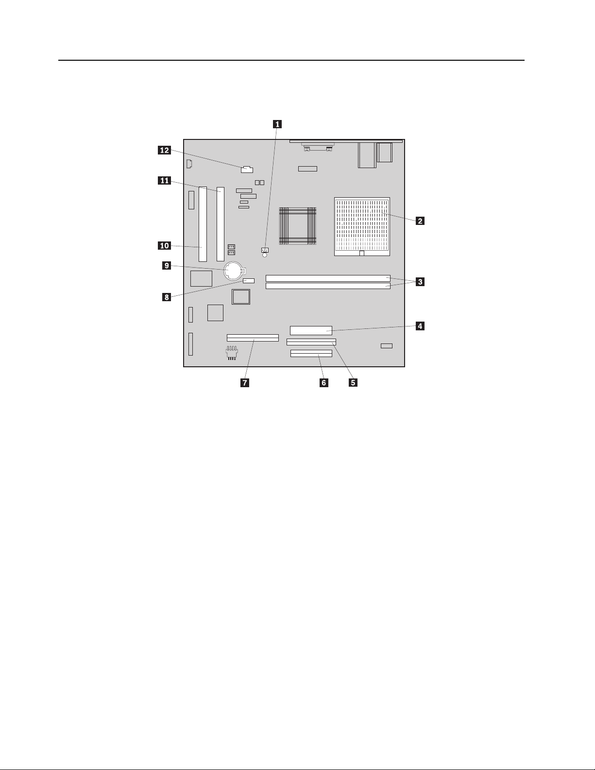
System board
The system board might look slightly different from the one shown.
Top of Monitor
Table 1.
?1Ý Fan connector ?7Ý Hard disk drive
connector
?2Ý Microprocessor ?8Ý CMOS clear jumper
?3Ý DIMM sockets ?9Ý Battery
?4Ý Power connector ?10Ý PCI expansion slot 1
?5Ý CD-ROM or DVD-
ROM drive connector
?6Ý Diskette drive
connector
?11Ý PCI expansion slot 2
?12Ý CD-ROM or DVD-R OM
drive audio connector
Cable connectors
The following connections for attaching devices are provided:
•USB (5)
•Mouse
•Keyboard
• Ethernet adapter with RJ-45 connector (some models only)
• Modem (some models only)
• Integrated audio controller with line in, line out, and microphone connectors
8 Technical Information
Page 17
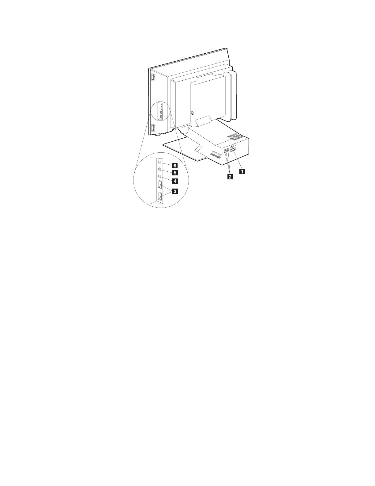
Þ1Ý Power cord connector
Þ2Ý USB connectors (3)
Þ3Ý USB connectors (2)
Þ4Ý Audio line in
Þ5Ý Audio line out
Þ6Ý Microphone
Chapter 2. System board fea tures 9
Page 18
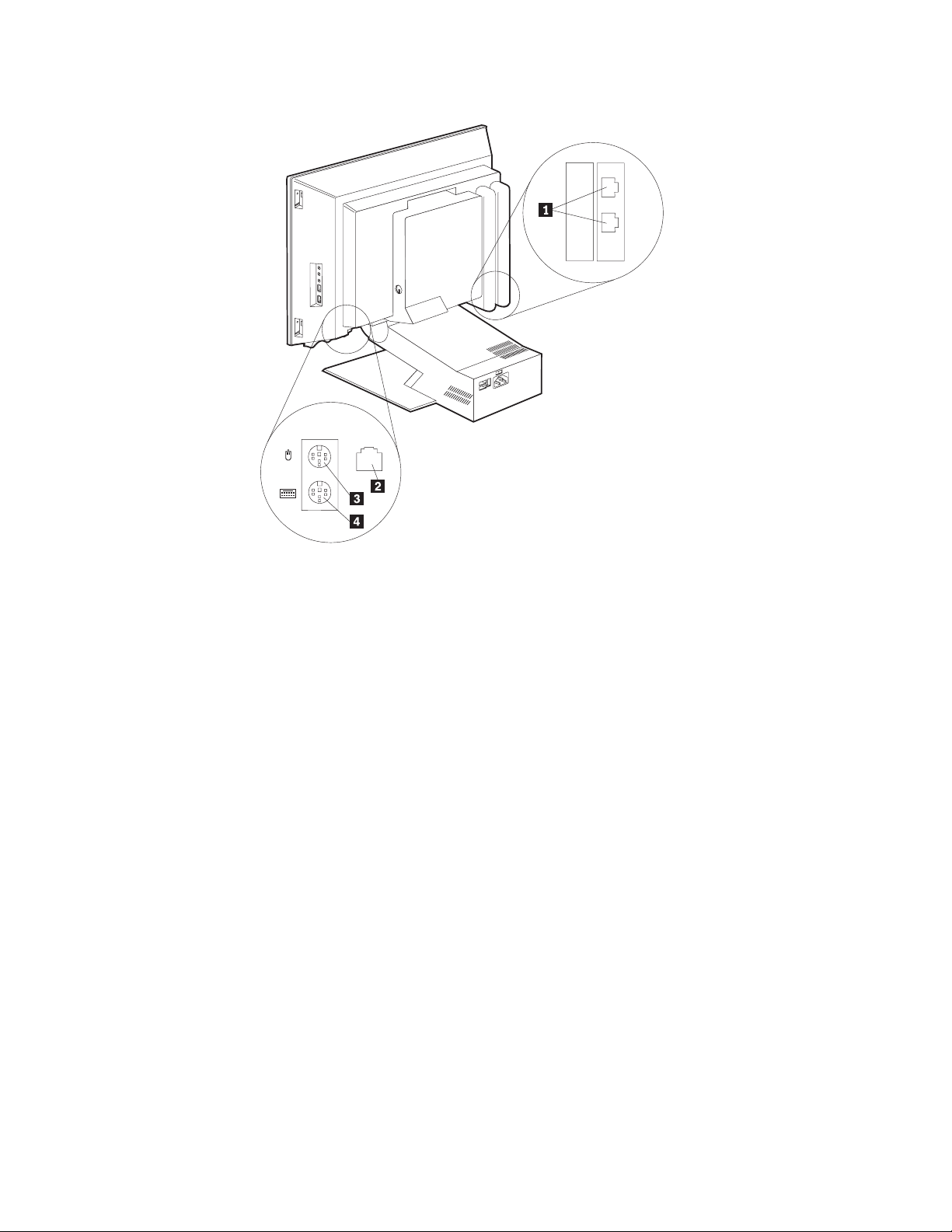
Þ1Ý Modem connectors
Þ2Ý Ethernet connector
Þ3Ý PS/2 mouse connector
Þ4Ý PS/2 keyboard connector
10 Technical Information
Page 19

Chapter 3. System specifications
This appendix provides the hardware specifications for your computer.
Dimensions
• Depth: 26.7 cm (10.5 in.)
• Width: 40.6 cm (16 in.)
• Height: 41.9 cm (16.5 in.)
Computer weight
• Maximum configuration (as shipped): 9.5 kg (21 lb.)
Environment
• Air temperature:
— System on: 5º to 35º C (41º to 95º F) at altitude 0-2134 m (7000 ft.)
— System off: -10º to 60º C (14º to 140º F)
• Humidity:
— System on: 10% to 80%
— System off: 10% to 90%
Electrical input
• Sine-wave input (50/60 Hz) is required
•Input voltage/current
—Low range:
– Minimum: 100 V ac
– Maximum: 127 V ac
– Current rating: 5.0 amps
— High range:
– Minimum: 200 V ac
– Maximum: 240 V ac
– Current rating: 3.0 amps
— Input kilovolt-amperes (kVA) (approximately):
– Maximum (configuration as shipped): .35 kVa
Note: Power consumption and heat output vary depend ing on the number
and type of optional features inst alled and the power-management
optional features in us e.
Heat output
• Approximate heat output in British thermal units (Btu) per ho ur:
— Maximum configuration (as shipped): 308 Btu/hour (90 watts)
1
— Maximum configuration (typical)
: 240 Btu/hour (70 watts)
1.Under typical maximum configurati on s, the heat output will be subst ant ia lly below the theoretical maximum.
© Copyright IBM Corp. 2000 11
Page 20

Acoustical noise-emission values
Average sound-pressure levels:
4.6 bels idle
5.0 bels operating
Note: These levels were measured in controlled acoustical envir onments accor ding
to procedures specified by the American National Standards Institute (ANSI)
S12.10 and ISO 7779, and are reported in accordance with ISO 9296. Actual
sound-pressure levels in your location might exceed the average values stated
because of room reflections and other nearby noise sources. The declared
sound power levels indicate an upper limit, below which a large number of
computers will operate.
12 Technical Information
Page 21

Chapter 4. Power supply
A 110-watt pow e r supply drives your computer. The power supply converts the ac
input voltage into four dc output voltages and provides power for the follow ing:
•System board
•Adapters
• Interna l d riv es
• Keyboard and auxiliary devices
•USB devices
Power input
The following table shows the power input specifications. The power supply has a
manual switch to select the correct input voltage.
Table 8. Power input requirements
Specification Measurements
Input voltage, low range 100 (min) to 127 (max) V ac
Input voltage, high range 200 (min) to 240 (max) V ac
Power output
Input frequency 50 Hz ± 3 Hz or 60 Hz ± 3 Hz
The power supply provides 3.3-volt power for the Pentium III microprocessor, core
chip set, and 5-volt power for PCI adapters. Also included is an auxiliary 5-volt (AUX
5) power supply to provide power to power-management circuitry and a Wake on
LAN adapter.
A logic signal on the power connector controls the power supply; the front panel
switch is not directly connected to the power supply.
The power supply connects to the system board with a 2 x 10 pin connector.
The following figures show the power supply output of all the conn ectors, including
the system board, DASD, PCI, and auxiliary outputs.
Table 9. Power output (110 watts)
Output voltage Tolerance Minimum current Maximum current
+5 V dc +5% to -5% 1.5 A 10.0 A
+12 V dc +5% to -5% 0.3 A 2.0 A
-12 V dc +10% to -10% 0.0 A 0.12 A
+3.3 V dc +5% to -5% 0.0 A 6.0 A
© Copyright IBM Corp. 2000 13
Page 22

Table 9. Power output (110 watts)
Output voltage Tolerance Minimum current Maximum current
+5 V ac (auxiliary) +5% to -5% 0.0 A 3.0 A
Component outputs
The power supply provides separate voltage sources for the syst em board and
internal storage devices. The following figures show the approximate power that is
provided for specific system components. Many components draw less current than
the maximum shown.
Table 10. System board
Supply voltage Maximum current Tolerance
+3.3 V dc 5000 mA +5.0% to -5.0%
+5.0 V dc 6000 mA +5.0 to -4.0%
+12.0 V dc 25.0 mA +5.0% to -5.0%
-12.0 V dc 25.0 mA +10.0% to -9.0%
Table 11. Keyboard port
Supply voltage Maximum current Tolera nce
+5.0 V dc 275 mA +5.0% to -4.0%
Table 12. Auxiliary device port
Supply voltage Maximum current Tolerance
+5.0 V dc 300 mA +5.0% to -4.0%
Table 13. PCI-bus adapters (per slot)
Supply voltage Maximum current Tolerance
+5.0 V dc 1000 mA +5.0% to -4.0%
+3.3 V dc 1500 mA +5.0% to -4.0%
Note: For each PCI connector, the maximum power consumption is rated at 5 watts
for +5 V dc and +3.3 V dc combined. If maximum power is used, the overall
system configuration will be limited in performance.
Table 14. USB port
Supply voltage Maximum current Tolerance
+5.0 V dc 500 mA +5.0%to -4.0%
14 Technical Information
Page 23

Table 15. Internal DASD
Supply voltage Maximum current Tolerance
+5.0 V dc 1400 mA +5.0% to -5.0%
+12.0 V dc 1500 mA at startup, 400 mA
Table 16. Video port pin 9
Supply voltage Maximum current Tolerance
+5.0 V dc 1100 mA +5.0% to -5.0%
Note: Some adapters and hard disk drives draw more current than the rated
Output protection
The power supply protects against output overcurrent, overvoltage, and short
circuits. See the power supply specifications on the previous pages for details.
A short circuit that is placed on any dc output (between outputs or between an output
and a dc return) latches all dc outputs into a shutdown state, with no damage to the
power supply. If this shutdown state occurs, the power supply returns to normal
operation only after the fault has been removed and the power switch has been
turned off for at least two seconds.
+5.0% to -5.0%
when active
maximums. These adapters and drives can be installed in the system;
however , the power supply will shut down if the total power used exceeds
the maximum power that is available.
If an overvoltage fault occurs (in the power supply), the power supply latches all dc
outputs into a shutdown state before any output exceeds 130% of the power supply
value.
Connector description
The power supply for your computer has four, 4- pin connectors for internal devices.
The total power used by the connectors must not exceed the amount shown in
“Component outputs” on page 14. For connector pin assignments, see “Appendix A.
Connector pin assignments,” on page 21.
Chapter 4. Power supply 15
Page 24

16 Technical Information
Page 25

Chapter 5. System software
This section briefly describes some of the system software included with your
computer.
BIOS
Your personal computer uses the IBM basic input/output system (BIOS), which is
stored in flash electrically erasable programmable read-only memory (EEPROM).
Some features of the BIOS are:
• PCI support according to PCI BIOS Specification 2.2
• Microsoft PCI IRQ Routing Table
• Plug and Play support according to Plug and Play BIOS Specification 1.1a
• Advanced Power Management (APM) support according to APM BIOS Interface
Specification 1.2
• Wake on LAN support
• Wake on Ring support
• Flash-over-LAN support
• Alternate startup sequence
• IBM Look and Feel - such as screen arrangements and user interface
• ACPI (Advanced Configuration and Power Interface)
• IDE Logical Block Addressing (LBA)
• LSA 2.0 support
• Digital optical disk support
• LS-120 disk drive support
• DM BIOS 2.1 (DMI 2.0 compliant)
• PC99 compl i ance
Plug and Play
Support for Plug and Play conforms to the following:
• Plug and Play BIOS Specification 1.1a and 1.0
• Plug and Play BIOS Extension Design Guide
• Plug and PLay BIOS Specification, Errata, and Clarifications 1.0
• Guide to Integrating the Plug and Play BIOS Extensions with system BIOS 1.2
• Plug and Play Kit for DOS and Windows
POST
IBM power-on self-test (POST) code is used. Also, initialization code is included for
the on-board system devices and controllers.
POST error codes include text messages for determining the cause of an error. For
more information, see “Appendix D. Error codes,” on page 41 and your User Guide.
Configuration/Setup Utility program
The Configuration/Setup Utility program provides menu ch oices f or de vices, I/O
ports, date and time, system security, start options, advanced setup, and power
management.
© Copyright IBM Corp. 2000 17
Page 26

More detailed information on using the Configuration/Setup Utility program is in the
PC 300GL and PC 300PL User Guide.
Advanced Power Management (APM)
Y ou r comput er has bu ilt-in ener gy-sa ving ca pabili ties. Advanc ed Power Ma nageme nt
(APM) is a feature that reduces the power consumption of components when they are
not in use. When enabled, APM initiates reduced-power modes for the monitor,
microprocessor, and hard disk drive after a specif ied period of inactivity.
The BIOS supports APM 1.2. This enables the system to enter a power-management
state, reducing the power drawn from the AC electrical outlet. Advanced Power
Management is enabled through the Configuration/Setup Utility program and is
controlled by the individual operating system.
For more information on APM, see the User Guide.
Advanced Configuration and Power Interface (ACPI)
Advanced Configuration and Power Interface (ACPI) BIOS mode enables the
operating system to control the power-management features of your computer. Not
all operating systems support ACPI BIOS mode. Refer to your operating-system
documentation to determine if ACPI is supported.
Flash update utility program
The flash update utility program is a stand-alone program to support flash updates.
This utility program updates the BIOS code and the machine readable information
(MRI) to different languages.
The latest version of the flash update utility program is available on the IBM Web site
at http://www.ibm.com/pc/support and can be copied to a 3.5-inch diskette.
Diagnostic program
The diagnostic program that comes with your computer is provided as a startable
IBM Enhanced Diagnostic diskette image on the IBM Product Recovery CD. It runs
independently of the operating system. The user interface is WaterGate Software PCDoctor. The diagnostic program can also be downloaded from
http://www.ibm.com/pc/support/ on the World Wide Web. For more info rmatio n
on the diagnostic program, see the User Guide.
18 Technical Information
Page 27

Chapter 6. System compatibility
This chapter discusses some of the hardware, software, and BIOS compatibility issues
for the computer. See the Compatib ility Report under, “Related publications” on page
vii for a list of compatible hardware and software options.
Hardware compatibil ity
This section discusses hardware, software, and BIOS compatibility that must be
considered when designing application programs.
The functional interfaces are compatible with the following interfaces:
• Intel 8259 interrupt controllers (edge-triggered mode)
• Motorola MC146818 Time of Day Clock command and status (CMOS
reorganized)
• Intel 8254 timer, driven from a 1.193 MHz clock (channels 0, 1, and 2)
• Intel 8237 DMA controller, except for the Command and Request registers and
the Rotate and Mask functions; the Mode register is partially supported
• Intel 8272 or 82077 diskette drive controllers
• Intel 8042 keyboard controller at address hex 0060 and hex 0064
• All video standards using VGA, EGA, CGA, MDA, and Hercules modes
Use this information to develop application programs. Whenever possible, use the
BIOS as an interface to hardware to provide maximum compatibi lity and portability
of applications among systems.
Hardware interrupts
Hardware interrupts are level-sensitive for PCI interrupts. The interrupt controller
clears its in-service register bit when the interrupt routine sends and End-of-Interrupt
(EOI) command to th e cont roller. Th e EOI com man d is s e nt regardless of whether the
incoming interrupt request to the controller is active or inactive.
The interrupt-in-progress latch is readable at an I/O-address bit position. This latch is
read during the interrupt service routine and might be reset by the read operation or it
might require an explicit reset.
Note: For performance and latency considerations, de signers might want to limit
the number of devices sharing an interrupt level.
With level-sensitive interrupts, the interrupt control ler requires that the interrupt
request be inactive at the time the EOI command is sent; otherwise, a new interrupt
request will be detected. To avoid this, a level-sensitive interrupt handler must clear
the interrupt condition (usually by a read or write operation to an I/O port on the
device causing the interrupt). After processing the interrupt, the interrupt handler:
1. Clears the interrupt
2. Waits one I/O delay
3. Sends the EOI
4. Waits one I/O delay
5. Enables the interrupt through the Set Interrupt Enable Flag command
© Copyright IBM Corp. 2000 19
Page 28

Hardware interrupt IRQ9 is defined as the replacement interrupt level for the cascade
level IRQ2. Program interrupt sharing is implemented on IRQ2, interrupt hex 0A. The
following processing occurs to maintain compatibility with the IRQ2 used by IBM
Personal Computer products:
1. A device drives the interrupt request active on IRQ2 of the channel.
2. This interrupt request is mapped in hardware to IRQ9 input on the second
interrupt controller.
3. When the interrupt occurs, the system microprocessor passes control to the IRQ9
(interrupt hex 71) interrupt handler.
4. This interrupt handler performs an EOI command to the second interrupt
controller and passes control to the IRQ2 (interrupt hex 0A) interrupt handler.
5. This IRQ2 interrupt handler, when handling the interrupt, causes the device to
reset the interrupt request before performing an EOI command to the master
interrupt controller that finishes servicing the IRQ2 request.
Software compatibility
To maintain software compatibility, the interrupt polling mech anism that is used by
IBM Personal Computer products is retained. Software that interfaces with the reset
port for the IBM Personal Computer positive-edge interrupt sharing (hex address
02Fx or 06Fx, where x is the interrupt level) does not create interference.
Software interrupts
With the advent of software interrupt sharing, software interrupt routines must daisy
chain interrupts. Each routine must check the function value, and if the function value
is not in the range of function calls, that routine must transfer control to the next
routine in the chain. Because software interrupts are initially pointed to address 0:0
before daisy chaining, check for this case. If the next routine is pointed to address 0:0
and the function call is out of range, the appropriate action is to set the carry flag and
initiate a RET 2 to indicate an error condition.
Machine-sensitive programs
Programs can select machine-specific features, but they must first identify the
machine and model type. IBM has defined methods for uniquely determining the
specific machine type. The machine model byte can be found through interrupt 15H,
Return System Configuration Parameters function (AH)=(C0H).
20 Technical Information
Page 29
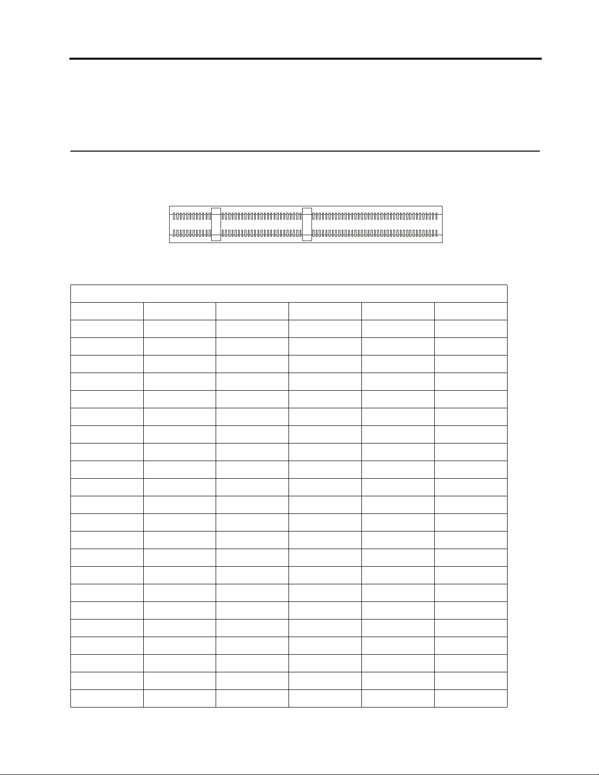
Appendix A. Connector pin assignments
The following figures show the pin assignments for various system board connectors.
System memory connector
85
1
Table 20. System memory connector pin assignments
Pin x64 nonparity x72 ECC Pin x64 nonparity x72 ECC
1 VSS VSS 85 VSS VSS
2 DQ0 DQ0 86 DQ32 DQ32
3 DQ1 DQ1 87 DQ33 DQ33
4 DQ2 DQ2 88 DQ34 DQ34
5 DQ3 DQ3 89 DQ35 DQ35
6 VCC VCC 90 VCC VCC
7 DQ4 DQ4 91 DQ36 DQ36
8 DQ5 DQ5 92 DQ37 DQ37
9 DQ6 DQ6 93 DQ38 DQ38
168
84
10 DQ7 DQ7 94 DQ39 DQ39
11 DQ8 DQ8 95 DQ40 DQ40
12 VSS VSS 96 VSS VSS
13 DQ9 DQ 97 DQ41 DQ41
14 DQ10 DQ10 98 DQ42 DQ42
15 DQ11 DQ11 99 DQ43 DQ43
16 DQ12 DQ12 100 DQ44 DQ44
17 DQ13 DQ13 101 DQ45 DQ45
18 VCC VCC 102 VCC VCC
19 DQ14 DQ14 103 DQ46 DQ46
20 DQ15 DQ15 104 DQ47 DQ47
21 NC CB0 105 NC CB4
22 NC CB1 106 NC CB5
© Copyright IBM Corp. 2000 21
Page 30

Table 20. System memory connector pin assignments
Pin x64 nonparity x72 ECC Pin x64 nonparity x72 ECC
23 VSS VSS 107 VSS VSS
24 NC NC 108 NC NC
25 NC NC 109 NC NC
26 VCC VCC 110 VCC VCC
27 /WE /WE0 111 /CAS /CAS
28 DQMB0 DQMB0 112 DQMB4 DQMB4
29 DQMB1 DQMB1 113 DQMB5 DQMB5
30 /S0 /S0 114 NC /S1
31 DU NC 115 /RAS /RAS
32 VSS VSS 116 VSS VSS
33 A0 A0 117 A1 A1
34 A2 A2 118 A3 A3
35 A4 A4 119 A5 A5
36 A6 A6 120 A7 A7
37 A8 A8 121 A9 A9
38 A10/AP A10/AP 122 BA0 BA0
39 NC BA1 123 NC A11
40 VCC VCC 124 VCC VCC
41 VCC VCC 125 CK1 CK1
42 CK0 CK0 126 A12 A12
43 VSS VSS 127 VSS VSS
44 DU NC 128 CKE0 CKE0
45 /S2 /S2 129 NC /S3
46 DQMB2 DQMB2 130 DQMB6 DQMB6
47 DQMB3 DQMB3 131 DQMB7 DQMB7
48 DU NC 132 A13 A13
49 VCC VCC 133 VCC VCC
50 NC NC 134 NC NC
51 NC NC 135 NC NC
52 NC CB2 136 NC CB6
53 NC CB3 137 NC CB7
54 VSS VSS 138 VSS VSS
55 DQ16 DQ16 139 DQ48 DQ48
56 DQ17 DQ17 140 DQ49 DQ49
57 DQ18 DQ18 141 DQ50 DQ50
22 Technical Information
Page 31

Table 20. System memory connector pin assignments
Pin x64 nonparity x72 ECC Pin x64 nonparity x72 ECC
58 DQ19 DQ19 142 DQ51 DQ51
59 VCC VCC 143 VCC VCC
60 DQ20 DQ20 144 DQ52 DQ52
61 NC NC 145 NC NC
62 NC NC 146 NC NC
63 NC CKE1 147 NC NC
64 VSS VSS 148 VSS VSS
65 DQ21 DQ21 149 DQ53 DQ53
66 DQ22 DQ22 150 DQ54 DQ54
67 DQ23 DQ23 151 DQ55 DQ55
68 VSS VSS 152 VSS VSS
69 DQ24 DQ24 153 DQ56 DQ56
70 DQ25 DQ25 154 DQ57 DQ57
71 DQ26 DQ26 155 DQ58 DQ58
72 DQ27 DQ27 156 DQ59 DQ59
73 VCC VCC 157 VCC VCC
74 DQ28 DQ28 158 DQ60 DQ60
75 DQ29 DQ29 159 DQ61 DQ61
76 DQ30 DQ30 160 DQ62 DQ62
77 DQ31 DQ31 161 DQ63 DQ63
78 VSS VSS 162 VSS VSS
79 CK2 CK2 163 CK3 CK3
80 NC NC 164 NC NC
81 NC NC 165 SA0 SA0
82 SKA SDA 166 SA1 SA1
83 SCL SCL 167 SA2 SA2
84 VCC VCC 168 VCC VCC
Table 21. System memory connector pin input/output
Pin Signal name I/O Pin Signal name I/O
1 GND N/A 85 GND N/A
2 MD0 I/O 86 MD32 I/O
3 MD1 I/O 87 MD33 I/O
4 MD2 I/O 88 MD34 I/O
5 MD3 I/O 89 MD35 I/O
Appendix A. Connector pin assignments 23
Page 32

Table 21. System memory connector pin input/output
Pin Signal name I/O Pin Signal name I/O
6 VDD I/O 90 VDD N/A
7 MD4 I/O 91 MD36 N/A
8 MD5 I/O 92 MD37 I/O
9 MD6 I/O 93 MD38 I/O
10 MD7 I/O 94 MD39 I/O
11 MD8 (PAR0) I/O 95 MD40 I/O
12 GND N/A 96 GND N/A
13 MD9 I/O 97 MD41 I/O
14 MD10 I/O 98 MD42 I/O
15 MD11 I/O 99 MD43 I/O
16 MD12 I/O 100 MD44 I/O
17 MD13 I/O 101 MD45 I/O
18 VDD N/A 102 VDD N/A
19 MD14 I/O 103 MD46 I/O
20 MD15 I/O 104 MD47 I/O
21 NC I/O 105 NC I/O
22 NC I/O 106 NC I/O
23 GND I/O 107 GND N/A
24 NC N/A 1 08 NC N/A
25 NC N/A 1 09 NC N/A
26 VDD N/A 110 VDD N/A
27 WE# I 111 CAS# N/A
28 DQMB0# I 112 DQMB4# I
29 DQMB1# I 113 DQMB4# I
30 S0# I 114 S1# I
31 OE0# I 115 RAS# N/A
32 GND N/ A 116 GND N/A
33 A0 I 117 A1 I
34 A2 I 118 A3 I
35 A4 I 119 A5 I
36 A6 I 120 A7 I
37 A8 I 121 A9 I
38 A10/ AP I 122 A11 I
39 NC 123 NC
40 VDD N/A 124 VDD N/A
24 Technical Information
Page 33

Table 21. System memory connector pin input/output
Pin Signal name I/O Pin Signal name I/O
41 NC N/A 125 CK1 N/A
42 CK0 N/A 126 A14 O
43 GND N/A 127 GND N/A
44 OE2# I 128 CKE0 N/A
45 S2# I 129 S3# I
46 DQMB2# I 130 DQMB6# I
47 DQMB3# I 131 DQMB7# I
48 WE2# I 132 A15 I
49 VDD N/A 133 VDD N/A
50 NC N/A 134 NC N/A
51 NC N/A 135 NC N/A
52 NC I/O 136 NC I/O
53 NC I/O 137 NC I/O
54 GND N/A 138 GND N/A
55 MD16 I/O 139 MD48 I/O
56 MD17 I/O 140 MD49 I/O
57 MD18 I/O 141 MD50 I/O
58 MD19 I/O 142 MD51 I/O
59 VDD N/A 143 VDD N/A
60 MD20 I/O 144 MD52 I/O
61 CKE1 N/A 145 NC N/A
62 VREF N/A 146 VREF N/A
63 (CKE1)* N/A 147 NC N/A
64 GND N/A 148 GND N/A
65 MD21 I/O 149 MD53 I/O
66 MD22 I/O 150 MD54 I/O
67 MD23 I/O 151 MD55 I/O
68 GND N/A 152 GND N/A
69 MD24 I/O 153 MD56 I/O
70 MD25 I/O 154 MD57 I/O
71 MD26 I/O 155 MD58 I/O
72 MD27 I/O 156 MD59 I/O
73 VDD N/A 157 VDD N/A
74 MD28 I/O 158 MD60 I/O
75 MD29 I/O 159 MD61 I/O
Appendix A. Connector pin assignments 25
Page 34
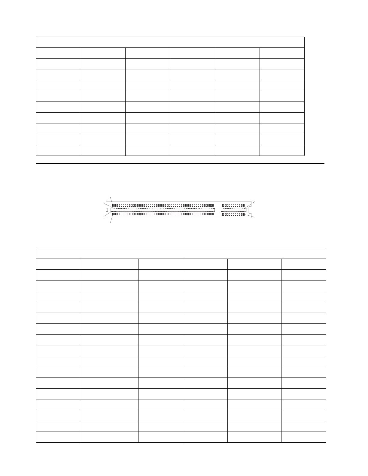
Table 21. System memory connector pin input/output
Pin Signal name I/O Pin Signal name I/O
76 MD30 I/O 160 MD62 I/O
77 MD31 I/O 161 MD63 I/O
78 GND N/A 162 GND N/A
79 CK2 O 163 CK3 O
80 NC N/A 1 64 NC N/A
81 NC O 165 SA0 O
82 SDA O 166 SA1 O
83 SCL O 167 SA0 O
84 VDD N/A 168 VDD N/A
PCI connectors
A1
A2
A62
B1
B2
B62
Table 22. PCI connector pin assignments
Pin Signal I/O Pin Signal I/O
A1 TRST# O B1 -12 V dc N/A
A2 +12 V dc N/A B2 TCK O
A3 +12 V dc O B3 Ground N/A
A4 TDI O B4 TDO I
A5 +5 V dc N/A B5 +5 V dc N/A
A6 INTA# I B6 +5 V dc N/A
A7 INTC# I B7 INTB# I
A8 +5 V dc N/A B8 INTD# I
A9 Reserved N/A B9 PRSNT1# I
A10 +5 V dc (I/O) N/A B10 Reserved N/A
A11 Reserved N/A B11 PRNST2 I
A12 Ground N/A B12 Ground N/A
A13 Ground N/A B13 Ground N/A
A14 Reserved N/A B14 Reserved N/A
A15 RST# O B15 Ground N/A
A16 +5 V dc (I/O) N/A B16 O O
26 Technical Information
Page 35

Table 22. PCI connector pin assignments
Pin Signal I/O Pin Signal I/O
A17 GNT# O B17 Ground N/A
A18 Ground N/A B18 REQ# I
A19 PCIPME N/A B19 +5 V dc (I/O) N/A
A20 Address/data 30 I/O B20 Address/data 31 I/O
A21 +3.3 V dc N/A B21 Address/data 29 I /O
A22 Address/data 28 I/O B22 Ground N/A
A23 Address/data 26 I/O B23 Address/data 27 I/O
A24 Ground I/O B24 Address/data 25 N/A
A25 Address/data 24 I/O B25 +3.3 V dc N/A
A26 IDSEL O B26 C/BE 3# I/O
A27 +3.3 V dc N/A B27 Address/data 23 I /O
A28 Address/data 22 I/O B28 Ground N/A
A29 Address/data 20 I/O B29 Address/data 21 I/O
A30 Ground I/O B30 Address/data 19 N/A
A31 Address/data 18 I/O B31 +3.3 V dc N/A
A32 Address/data 16 I/O B32 Address/data 17 I/O
A33 +3.3 V dc N/A B33 C/BE2# I/O
A34 FRAME# I/O B34 Ground N/A
A35 Ground N/A B35 IRDY# I/O
A36 TRDY# I/O B36 +3.3 V dc N/A
A37 Ground N/A B37 DEVSEL# I/O
A38 STOP# I/O B38 Ground N/A
A39 +3.3 V dc N/A B39 LOCK# I/O
A40 SDONE I/O B40 PERR# I/O
A41 SBO# I/O B41 +3.3 V dc N/A
A42 Ground N/A B42 SERR# I/O
A43 +3.3 V dc N/A B43 +3.3 V dc N/A
A44 C/BE(1)# I/O B44 C/BE 1# I/O
A45 Address/data 14 I/O B45 Address/data 14 I/O
A46 Ground N/A B46 Ground N/A
A47 Address/data 12 I/O B47 Address/data 12 I/O
A48 Address/data 10 I/O B48 Address/data 10 I/O
A49 Ground N/A B49 Ground N/A
A50 Key N/A B50 Key N/A
A51 Key N/A B51 Key N/A
Appendix A. Connector pin assignments 27
Page 36
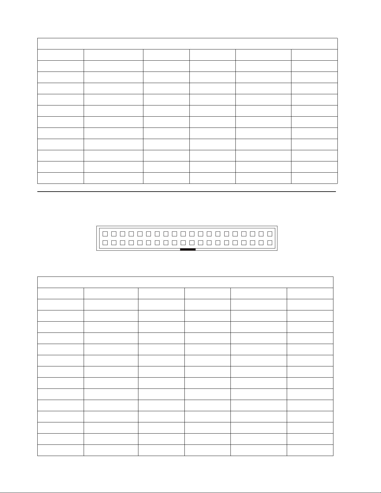
Table 22. PCI connector pin assignments
Pin Signal I/O Pin Signal I/O
A52 Address/data 8 I/O B52 A ddress/data 8 I/O
A53 Address/data 7 I/O B53 A ddress/data 7 I/O
A54 +3.3 V dc N/A B54 +3.3 V dc N/A
A55 Address/data 5 I/O B55 A ddress/data 5 I/O
A56 Address/data 3 I/O B56 A ddress/data 3 I/O
A57 Ground N/A B57 Ground N/A
A58 Address/data 1 I/O B58 A ddress/data 1 I/O
A59 +5 V dc (I/O) N/A B59 +5 V dc (I/O) N/A
A60 ACK64# I/O B60 ACK64# I/O
A61 +5 V dc N/A B61 +5 V dc N/A
A62 +5 V dc N/A A62 +5 V dc N/A
IDE connectors
2
1
40
39
Table 23. IDE connector pin assignments
Pin Signal I/O Pin Signal I/O
1 R ESET O 21 NC N/A
2GroundN/A22GroundN/A
3 Data bus bit 7 I/O 23 I/O write O
4 Data bus bit 8 I/O 24 NC N/A
5 D ata bus bit 6 I/O 25 I/O read O
6 Data bus bit 9 I/O 26 Ground I
7 Data bus bit 5 I/O 27 I/O channel ready I
8 Data bus bit 10 I/O 28 ALE O
9 Data bus bit 4 I/O 29 NC N/A
10 Data bus bit 11 I/O 30 Ground N/A
11 Data bus bit 3 I/O 31 IR Q I
12 Data bus bit 12 I/O 32 CS16# I
13 Data bus bit 2 I/O 33 SA1 O
14 Data bus bit 13 I/ O 34 PDIAG# I
28 Technical Information
Page 37

Table 23. IDE connector pin assignments
Pin Signal I/O Pin Signal I/O
15 Data bus bit 1 I/O 35 SA0 O
16 Data bus bit 14 I/O 36 SA2 O
17 Data bus bit 0 I/O 37 CS0# O
18 Data bus bit 15 I/O 38 CS1 O
19 Ground N/A 39 Active# I
20 Key (Reserved) N/A 40 Ground N/A
Appendix A. Connector pin assignments 29
Page 38

Diskette drive connector
2
1
34
33
Table 24. Diskette drive connector pin assignments
Pin Signal I/O Pin Signal I/O
1 Drive 2 installed # I 18 Direction in# O
2High density
O19 GroundN/A
select
3 Not connected N/A 20 Step# O
4 Not connected N/A 21 Ground N/A
5 Ground N/A 22 Write data # O
6 D ata rate 0 N/A 23 Ground N/A
7 Ground N/A 24 Write enable# O
8Index#I25GroundN/A
9 Reserved N/A 26 Track0# I
10 Motor enable 0# O 27 M SEN0 I
11 Ground N/A 28 Write protect# I
12 Drive select 1# O 29 Ground N/A
13 Ground N/A 30 Read data# I
14 Drive select 0# O 31 Ground N/A
15 Ground N/A 32 Head 1 select# O
16 Motor enable 1# O 33 Data rate 1 N/A
17 MSEN1 I 34 Diskette change# I
30 Technical Information
Page 39
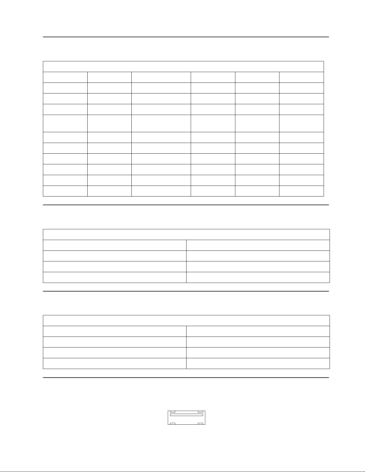
Power supply connector
Table 25. Power supply connector pin assignments
Pin Signal Function Pin Signal Function
1 3.3 V dc +3.3 V dc 11 3.3 V dc +3.3 V dc
2 3.3 V dc +3.3 V dc 12 -12 V dc -12 V dc
3COMGround13COMGround
4 5 V dc +5 V dc 14 PS-ON DC Remote
Enable
5COMGround15COMGround
6 5 V dc +5 V dc 16 COM Ground
7COMGround17COMGround
8 POK PWR GOOD 18 Reserved Reserved
9 5 VSB Standby Voltage 19 5 V dc +5 V dc
10 12 V dc +12 V dc 20 5 V dc +5 V dc
Wake on LAN connectors
Table 26. J14 Wake on LAN connector pin assignments
Pin Description
1 +5 V AUX
2Ground
3 Internal Wake on LAN
Alert on LAN connector
Table 26. Alert on LAN connector pin assignments
Pin Description
1Alert data
2Alert clock
3Intrusion
USB port connectors
1
3
Appendix A. Connector pin assignments 31
2
4
Page 40
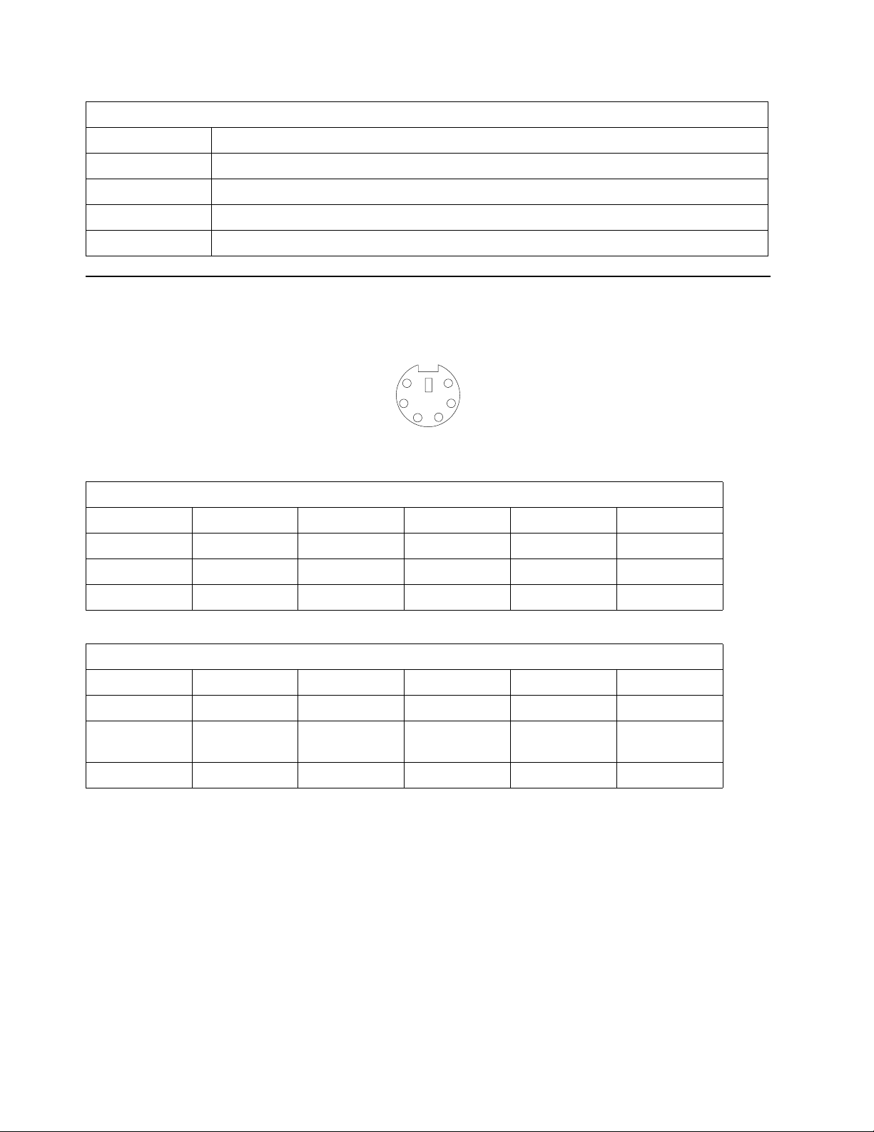
Table 27. USB port connector pin assignments
Pin Signal
1VCC
2-Data
3+Data
4Ground
Mouse and keyboard port connectors
6
4
2
5
3
1
Table 28. Mouse port connector pin assignments
Pin Signal I/O Pin Signal I/O
1DataI/O4+5 V dcN/A
2 Reserved I/O 5 Clock I/O
3GroundN/A6ReservedN/A
Table 29. Keyboard port connector pin assignments
Pin Signal I/O Pin Signal I/O
1 Keyboard data I/O 4 +5 V dc N/A
2 Mouse data I/O 5 Keyboard
I/O
Clock
3GroundN/A6Mouse clockN/A
32 Technical Information
Page 41

Appendix B. System address maps
System memory map
The first 640 KB of system board RAM is mapped starting at address hex 0000000. A
256 byte area and a 1 KB area of this RAM are reserved for BIOS data areas. Memory
can be mapped differently if POST detects an error.
Table 32. System memory map
Address range
(decimal)
0–512 KB 00000–7FFFF 512 KB Con ventional
512–639 KB 80000–9FBFF 127 KB Extended conventional
639–640 KB 9FC00–9FFFF 1 KB Extended BIOS data
640–767 KB A0000–BFFFF 128 KB Dynamic video memory display
768–800 KB C0000–C7FFFF 32 KB Video ROM BIOS (shadowed)
800–896 KB C8000–DFFFF 96 KB PCI space, available to adapter
896 KB–1 MB E0000–FFFFF 128 KB System ROM BIOS (main memory
1–16 MB 100000–FFFFFF 15 MB PCI space
16–4096 MB 1000000–FFDFFFF 4080 MB PCI space (positive decode)
4096–4120 MB FFFE0000–FFFFFFFF 128 KB System ROM BIOS
Address range (hex) Size Description
cache
ROMs
shadowed)
© Copyright IBM Corp. 2000 33
Page 42

Input/output address map
The following lists resource assignments for the I/O address map. Any addresses that
are not shown are reserved.
Table 33. I/O address map
Address (hex) Size Description
0000–000F 16 bytes DMA 1
0010–001F 16 bytes General I/O locations - available to PCI bus
0020–0021 2 bytes Interrupt controller 1
0023–003F 30 bytes General I/O locations - available to PCI bus
0040–0043 4 bytes Counter/timer 1
0044–00FF 28 bytes General I/O locations - available to PCI bus
0060 1 byte Keyboard controller byte - reset IRQ
0061 1 byte System port B
0064 1 byte Keyboard controller, CMB/STAT byte
0070, bit 7 1 bit Enable NMI
0070, bits 6:0 1 bit Real-time clock, address
0071 1 byte Real-time clock, data
0072–007F 14 bytes General I/O locations - available to PCI bus
0080 1 byte POST checkpoint register during POST only
008F 1 byte Refresh page register
0080–008F 16 bytes ICH1, DMA page registers
0090–0091 15 bytes General I/O locations - available to PCI bus
0092 1 byte PS/2 keyboa rd controller registers
0093–009F 15 bytes General I/O locations
00A0–00A1 2 bytes Interrupt controller 2
00A2–00BF 30 bytes APM control
00C0–00DF 31 bytes DMA 2
00E0–00EF 16 bytes General I/O locations - available to PCI bus
00F0 1 byte Coprocessor error register
00F1–016F 127 bytes General I/O locations - available to PCI bus
0170–0177 8 bytes Secondary IDE channel
01F0–01F7 8 bytes Primary IDE channel
0200–0207 8 bytes Available
0220–0227 8 bytes Serial port 3 or 4
0228–0277 80 bytes General I/O locations - available to PCI bus
0278–027F 8 bytes Available
34 Technical Information
Page 43

Table 33. I/O address map
Address (hex) Size Description
0280–02E7 102 bytes Available
02E8–02EF 8 bytes Serial port 3 or 4
02F8–02FF 8 bytes IR
0338–033F 8 bytes Serial port 3 or 4
0340–036F 48 bytes Available
0370–0371 2 bytes SIO planar Plug and Play index/data registers
0372–0375 4 bytes Available
0376–0377 2 bytes IDE channel 1 command
0378–037F 8 bytes Available
0380–03B3 52 bytes Available
03B4–03B7 4 bytes Video
03BA 1 byte Video
03BC–03BE 16 bytes Reserved
03C0–03CF 16 bytes Video
0334–03D7 4 bytes Video
03DA 1 byte Video
03D0–03DF 11 bytes Available
03E0–03E7 8 bytes Available
03E8–03EF 8 bytes COM3 or COM4
03F0–03F5 6 bytes Diskette channel 1
03F6 1 byte Primary IDE channel command port
03F7 (Write) 1 byte Diskette channel command
03F7, bit 7 1 bit Diskette disk change channel
03F7, bits 6:0 7 bits Primary IDE channel status port
03F8–03FF 8 bytes Internal debug
0400–047F 128 bytes Available
0480–048F 16 bytes DMA channel high page registers
0490–0CF7 1912 bytes Available
0CF8–0CFB 4 bytes PCI configuration ad dress register
0CFC–0CFF 4 bytes PCI configuration date register
Open–400h 8 bytes ECP port, LPTn base address + hex 400
0CF9 1 byte Turbo and reset control register
0D00–FFFF 62207 bytes Available
Appendix B. System address maps 35
Page 44

DMA I/O address map
Table 34. DMA I/O address map
Address (hex) Description Bits Byte pointer
0000 Channel 0, Memory Address register 00–15 Yes
0001 Channel 0, Transfer Count register 00–15 Yes
0002 Channel 1, Me mory Address register 00–15 Yes
0003 Channel 1, Transfer Count register 00–15 Yes
0004 Channel 2, Me mory Address register 00–15 Yes
0005 Channel 2, Transfer Count register 00–15 Yes
0006 Channel 3, Me mory Address register 00–15 Yes
0007 Channel 3, Transfer Count register 00–15 Yes
0008 Channels 0–3, Read Status/Write Command
register
0009 Channels 0–3, Write Request register 00–02
000A Channels 0–3, Write Single Mask register bits 00–02
000B Channels, 0–3, Mode register (write) 00–07
000C Channels 0–3, Clear byte pointer (write) N/A
000D Channels, 0–3, Master clear (writer)/temp (read) 00–07
000E Channels 0–3, Clear Mask register (write) 00–03
000F Channels 0–3, Write All Mask register bits 00–03
0081 Channel 2, Page Table Address register 00–07
0082 Channel 3, Page Table Address register 00–07
0083 Channel 1, Page Table Address register 00–07
0087 Channel 0, Page Table Address register 00–07
0089 Channel 6, Page Table Address register 00–07
008A Channel 7, Page Table Address register 00–07
008B Channel 5, Page Table Address register 00–07
008F Channel 4, Page Table Address/Refresh register 00–07
00–07
00C0 Channel 4, Memory Address register 00 –15 Yes
00C2 Channel 4, Transfer Count register 00–15 Yes
00C4 Channel 5, Memory Address register 00 –15 Yes
00C6 Channel 5, Transfer Count register 00–15 Yes
00C8 Channel 6, Memory Address register 00 –15 Yes
00CA Cha nnel 6, Transfer Count register 00–15 Yes
00CC Channel 7, Memory Address register 00–15 Yes
36 Technical Information
Page 45

Table 34. DMA I/O address map
Address (hex) Description Bits Byte pointer
00CE Channel 7, Tra nsfer Count register 00–15 Yes
00D0 Channels 4–7, Read Status/Write Command
register
00D2 Channels 4–7, Write Request register 00–02
00D4 Channels 4–7, Write Single Mask register bit 00–02
00D6 Channels 4–7, Mode register (write) 00–07
00D8 Channels 4–7, Clear byte pointer (write) N/A
00DA Channels 4–7, Master clear (write)/temp (read) 00–07
00DC Channels 4–7, Clear Mask register (write) 00–03
00DE Channels 4–7, Write All Mask register bi ts 00–03
00DF Channels 507, 8- or 16-bit mode select 00–07
00–07
PCI configuration space map
Table 35. PCI configuration space map
Bus number (hex) Device number (hex) Function number (hex) Description
00 00 00 Host Bridge
00 00 01 IDE controller
00 01 00 ISA Bridge
00 01 01 Ethernet network
00 01 02 Universal Serial Bus
00 01 03 Universal Serial Bus
00 01 04 Audio Multimedia
00 02 00 PCI to PCI Bridge
00 05 00 Ethernet or modem
01 00 00 VGA Graphics
Appendix B. System address maps 37
Page 46

38 Technical Information
Page 47

Appendix C. IRQ and DMA channel assignments
The following tables list the interrupt request (IRQ) and direct m emory access (DMA
channel assignments.
Table 36. IRQ channel assignments
IRQ System resource
NMI Critical system error
SMI System management inte rrupt - power management
0 Reserved (interval timer)
1PS/2 keyboard
2 Reserved
3 available to user
4 Reserved (for internal debug)
5ACPI
6 Diskette controller
7 Available to user
8 Real-time clock
9 Ethernet controller/PCI to USB open host controller/Audio driver
10 Available to user
11 Available to user
12 PS/2 Mouse
13 Reserved (math coprocessor)
14 Primary IDE (if present)
15 Secondary IDE (if present)
© Copyright IBM Corp. 2000 39
Page 48

Table 37. DMA channel assignments
DMA channel Data width System resource
0 8 bits Open
1 8 bits Open
2 8 bits Diskette drive
3 8 bits Open
4 8 bits Direct memory access controller
516 bitsOpen
616 bitsOpen
716 bitsOpen
40 Technical Information
Page 49

Appendix D. Error codes
A complete list of POST codes is provided in the User Guide and in the Hardware
Maintenance Manual for your computer.
POST error codes
POST error messages appear when, during startup, POST finds problems with the
hardware or a change in the hardware configuration. POST error messages are 3-, 4-,
5-, 8-, or 12-character alphanumeric messages.
© Copyright IBM Corp. 2000 41
Page 50

42 Technical Information
Page 51

Bibliography
The following publications were reference materials
for IBM. This list of reference materials is provided
for convenience only. For further information on
these materials, contact the source corporation.
• Advanced Power Management (APM) BIOS
Interface Specification 1.2, source: Intel
Corporation
• AT Attachm ent Interface with Extension s, source:
American National Standard of Accredited
Standards Committee
• Extended Capabilities Port: Specification Kit,
source: Microsoft Corporation
• Intel Microprocessor and Peripheral Component
Literature, source: Intel Corporation
• PCI BIOS Specification 2.0, source: PCI Special
Interest Group
• Plug and Play BIOS Specification 1.1, source:
Microsoft Corporation;
http://www.microsoft.com/hwdev/
• Plug and Play BIOS Specification for Windows
2000, source: Microsoft Corporation
• Plug and Play BIOS Specification, Errata and
Clarifications 1.0, source: Microsoft
Corporation
• Universal Serial Bus Specifications, source:
http://www.usb.org
• Video Electronics Standards Association 1.2,
source: http://www.vesa.org
© Copyright IBM Corp. 2000 43
Page 52

44 Technical Information
Page 53

Notices
This publication was developed for products and services offered in the U.S.A.
IBM may not offer the products, services, or features discussed in this document in
other countries. Consult your local IBM representative for information on the
products and services currently available in your area. Any reference to an IBM
product, program, or service is not intended to state or imply that only that IBM
product, program, or service may be used. Any functionally equivalent product,
program, or service that does not infringe any IBM intellectua l property right ma y be
used instead. However, it is the user’s responsibility to evaluate an d verify the
operation of any non -IBM product, program, or service.
IBM may have patents or pending patent applica tions covering subject matter
described in this document. The furnishing of this document does not give you any
license to these patents. You can send license inquiries, in writing, to:
IBM Director of Licensing
IBM Corporation
North Castle Drive
Armonk, NY 10504-1785
U.S.A.
The following paragraph does not apply to the United Kingdom or any country
where such provisions are inconsiste nt with local law: INTERNATIONAL
BUSINESS MACHINES CORPORATION PROVIDES THIS PUBLICATION "AS IS"
WITHOUT WARRANTY OF ANY KIN D, EITHER EXPRESS OR IMPLIED,
INCLUDING, BUT NOT LIMITED TO, THE IMPLIED WARRANTIES OF NONINFRINGEMENT, MERCHANTABILITY OR FITNESS FOR A PARTICULAR
PURPOSE. Some states do not allow disclaimer of express or implied warranties in
certain transactions, therefore, this statement may not apply to you.
This information could include technical inaccuracies or typographical errors.
Changes are periodically made to the information herein; these changes will be
incorporated in new editions of the publication. IBM may make improvements
and/or changes in the product(s) and/or the program(s) described in this publication
at any time without notice.
Any references in this publication to non-IBM Web sites ar e pr ovided for convenience
only and do not in any manner serve as an endorsement of those Web sites. The
materials at those Web sites are not part of the materials for this IBM product, and use
of those Web sites is at your own risk.
IBM may use or distribute any of the information you supply in any way it believes
appropriate without incurring any obligation to you.
Processing date data
This IBM hardware product and IBM software products that might be packaged with
it have been designed, when used in accordance with their associated
documentation, to process date data correctly within and between the 20th and 21st
centuries, provided all other products (for example, software, hardware, and
firmware) used with these products properly exchange accurate date data with them.
© Copyright IBM Corp. 2000 45
Page 54

Trademarks
IBM cannot take responsibility for the date data processing capabilities of non-IBM
products, even if those products are preinstalled or otherwise distributed by IBM.
You should contact the vendors responsible for those products directly to determine
the capabilities of their products and update them if needed. This IBM hardware
product cannot prevent errors that might occur if software, upgrades, or peripheral
devices you use or exchange data with do not process date data correctly.
The foregoing is a Year 2000 Readiness Disclosure.
The following terms are trademarks of the IBM Corporation in the United States or
other countries or both:
•Alert on LAN
•IBM
NetVista
•
•PS/2
ScrollPoint
•
• Wake on LAN
Intel and Pentium are trademarks of Intel Corporation in the United States, other countr ies, or
both.
Microsoft and Windows are trademarks of Microsoft Corporation in the United States, other
countries, or both.
Other company, product, and service names may be trademarks or service marks of others.
46 Technical Information
Page 55

Index
A
ACPI 18
address maps
DMA I/O 36
input/output 34
PCI configuration 37
Adlib 6
ADSL modems 2
Advanced Configuration and Power
Interface 18
Advanced Power Management 18
APM 18
audio
connectors 6
controller 6
device drivers 6
subsystem 6
B
basic input/output system 17
bibliography 43
BIOS 17
bus
PCI 5
universal serial 5
C
channel assignments
DMA 40
IRQ 39
chip set 4
clock 7
CMOS 7
compatibility
hardware 19
software 20
component current 14
Configuration/Setup Utility 17
connector
cables 8
diskette drive 30
IDE 28
keyboard 32
mouse port 32
PCI 26
power supply 31
system memory 21
USB 31
Wake on LAN 31
D
DIMM 4
direct memory access 5
diskette drive
connector 30
DMA 5
DMA I/O address map 36
dual inline memory module 4
DVD-ROM 2
E
EEPROM 7
end-of-interrupt (EOI) 19
EOI (end-of-interrupt) 19
error codes
alphanumeric 41
complete lists 41
POST 41
Ethernet 7
expansion
adapters 7
PCI 7
slots 7
F
flash
EEPROM 7
update utility 18
G
GB viii
gigabyte viii
H
hardware interrup ts 19
hex viii
I
IDE
connector 28
input/output address map 34
integrated peripheral c ontroller 6
interrupts
hardware 19
PCI 19
software 20
K
keyboard po rt connector 32
kilobytes viii
M
machine model byte 20
machine-sensitive programs 20
major features 1
megabyte viii
memory
connectors 21
system 4
microprocessor 3
MMX 3
mouse 6
mouse port connector 32
N
network
Eathernet 7
O
overvoltage 15
P
PCI
connectors 26
interrupts 19
PCI configuration space map 37
PCI connector 26
pin assignments 21
Plug and Play 17
port
keyboard 6
mouse 6
POST 17
errors 41
Power
input, output 13
power
supply 15
supply connector 31
power-on self-test 17
publications, related vii
R
real-time clock 7
S
shutdown 15
SMID 1
software
CDs 18
compatibility 20
diagnostic program 18
SoundBlaster 6
system board 8
system memory map 33
U
Universal Serial Bus 5
USB
interface 5
port connectors 31
W
Wake on LAN 2
Wake on LAN connector 31
Wake on Ring 2
© Copyright IBM Corp. 2000 47
 Loading...