Microsemi Corporation SL15, SL03, SL05, SL12, SL24 Datasheet

SL03
8700 E. Thomas Road
Scottsdale, AZ 85251
Tel: (480) 941-6300
Fax: (480) 947-1503
TVSarray Series
DESCRIPTION (300 watt)
This 3 pin ULTRA LOW CAPACITANCE TRANSIENT VOLTAGE
SUPPRESSOR is designed for use in applications where protection is
required at the board level from voltage transients caused by
electrostatic discharge (ESD) as defined by IEC 1000-4-2, electrical
fast transients (EFT) per IEC 1000-4-4.
This product provides unidirectional protection for 1 line by connecting
the Input/Output line to pin 1, pin 2 to common or ground and pin 3 (is
not connected). The SL03 thru SL24 product provides board level
protection from static electricity and other induced-voltage surges that
can damage sensitive circuitry.
These TRANSIENT VOLTAGE SUPPRESSOR (TVS) Diode Arrays protect 3.0/3.3 Volt components such
as DRAM’s, SRAM’s, CMOS, HCMOS, HSIC, and low voltage interfaces up to 24 Volts. Because of the
physical size, weight and protection capabilities, this product is ideal for use in but not limited to
miniaturized electronic equipment such as hand held instruments, computers, computer peripherals and
cell phones.
thru
SL24
FEATURES
• Protects 3.0/3.3 up through 24V Components
• Protects 1 Unidirectional line
• Provides electrically isolated protection
• SOT-23 Packaging
MAXIMUM RATINGS
• Operating Temperatures: -55ºC to +150ºC
• Storage Temperature: -55
• SL03 thru SL24 have a Peak Pulse Power: 300 Watts
ºC to +150ºC
PACKAGING
• Tape & Reel EIA Standard 481
• 7 inch reel 5,000 pieces
• 13 inch reel 10,000 pieces
MECHANICAL
• Molded SOT-23 Surface Mount
• Weight: .014 grams (approximate)
• Body Marked with device number
(8/20 µsec, Figure 1)
• Pulse Repetition Rate: <.01%
ELECTRICAL CHARACTERISTICS @ 25ºC Unless otherwise specified
CLAMPING
VOLTAGE
V
C
@ 1 Amp
(FIGURE 2)
VOLTS
CLAMPING
VOLTAGE
V
C
@ 5 Amp
(FIGURE 2)
VOLTS
LEAKAGE
CURRENT
I
D
@ V
WM
µA
CAPACITANCE
@0V, 1 MHz
C
pF
WM
BREAKDOWN
VOLTAGE
V
BR
@1 mA
VOLTS
STAND
OFF
PART
NUMBER
SL03 L03 3.3 4 8 11 200 3 -5
SL05 L05 5.0 6.0 10.8 13 100 3 3
SL12 L12 12.0 13.3 19 26 1 3 10
SL15 L15 15.0 16.7 25 32 1 3 13
SL24 L24 24.0 26.7 44 57 1 3 30
DEVICE
MARKING
VOLTAGE
V
VOLTS
MAX MIN MAX MAX MAX MAX MAX
NOTE: Transient Voltage Suppression (TVS) product is normally selected based on its stand off Voltage VWM. Product
selected voltage should be equal to or greater than the continuous peak operating voltage of the circuit to be protected.
TEMPERATURE
COEFFICIENT
OF V
BR
á
VBR
mV/ºC
MSC1377.PDF ISO 9001 CERTIFIED REV C 1/27/2000

SL03 thru SL24
P
- PEAK PULSE POWER
WAVE FORMS
100
100
10
1.0
PP
.10
100ns 1µs 10µs 100µs 1ms 10ms
td – PULSE TIME - SEC
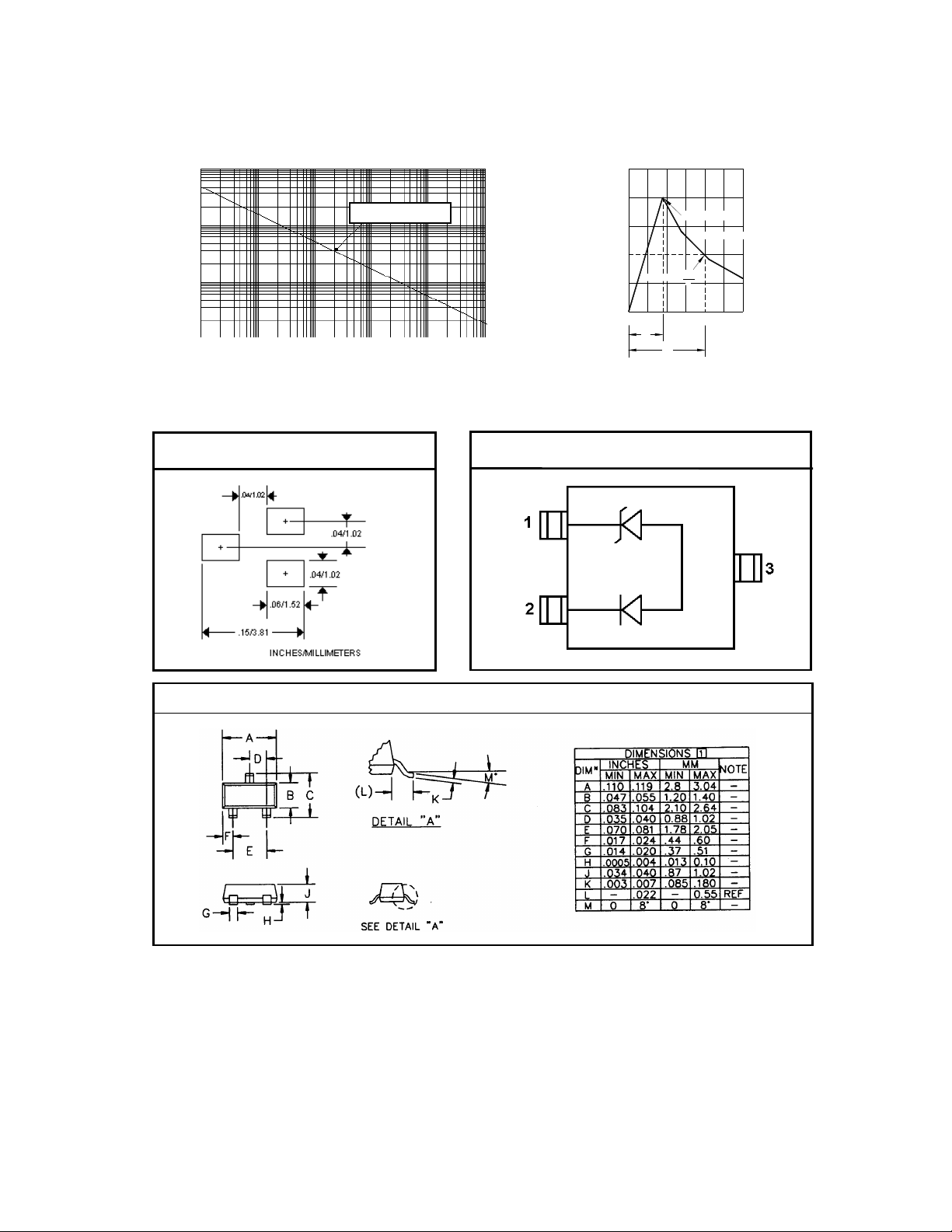
FIGURE 1
Peak Pulse Power Vs Pulse Time
8/20 µs 300 W pulse
50
Half-Value --
0
0
Ipp -- Peak Pulse Current -- % Ipp
10
t
t
d
t -- Time in microsec
FIGURE 2
Pulse Wave Form
MOUNTING PAD SOT23 CIRCUIT DIAGRAM
Peak Value -- Ipp
8 X 20 Waveform
Ipp
2
20 30
PACKAGE OUTLINE
MSC1377.PDF ISO 9001 CERTIFIED REV C 1/27/2000
 Loading...