Microsemi Corporation SG137AL, SG137AL-883B, SG137AL-DESC, SG137AT, SG137AT-883B Datasheet
...
SG137A/SG237A/SG337A
SG137/SG237/SG337
1.5 AMP NEGATIVE
ADJUSTABLE REGULATOR
DESCRIPTION
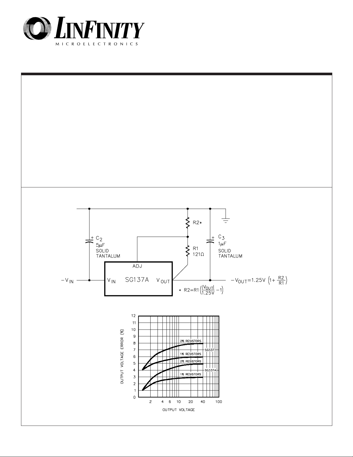
The SG137A family of negative adjustable regulators will deliver up to 1.5A
output current over an output voltage range of -1.2V to -37V. Silicon General
has made significant improvements in these regulators compared to previous
devices, such as better line and load regulation, and a maximum output voltage
error of 1%. The SG137 family uses the same chip design and guarantees
maximum output voltage error of ±2%.
Every effort has been made to make these devices easy to use and difficult to
damage. Internal current and power limiting coupled with true thermal limiting
prevents device damage due to overloads or shorts even if the regulator is not
fastened to a heat sink.
The SG137A/137 family of products are ideal complements to the SG117A/
117 adjustable positive regulators.
BLOCK DIAGRAM
FEATURES
••
• 1 % output voltage tolerance
••
••
• 0.01%/V line regulation
••
••
• 0.5% load regulation
••
••
• 0.02%/W thermal regulation
••
••
• Available in hermetic TO-220
••
HIGH RELIABILITY FEATURES
-SG137A/SG137
♦♦
♦ Available to MIL-STD-883 and DESC SMD
♦♦
♦♦
♦ Scheduled for MIL-M38510 QPL listing
♦♦
♦♦
♦ MIL-M38510/11804BYA - JAN137K
♦♦
♦♦
♦ LMI level "S" processing available
♦♦
2/92 Rev 1.1 2/94 LINFINITY Microelectronics Inc.
Copyright 1994 11861 Western Avenue
1 (714) 898-8121
∞ ∞
∞ Garden Grove, CA 92841
∞ ∞
∞∞
∞ FAX: (714) 893-2570
∞∞

ABSOLUTE MAXIMUM RATINGS (Note 1)
Power Dissipation ..........................................
Input to Output Voltage Differential ....................................
Storage Temperature Range ............................
Note 1. Exceeding these ratings could cause damage to the device.
Internally Limited
40V
-65°C to 150°C
THERMAL DATA
K Package:
Thermal ResistanceThermal Resistance-
R Package:
Thermal ResistanceThermal Resistance-
T Package:
Thermal ResistanceThermal Resistance-
IG Package:
Thermal ResistanceThermal Resistance-
L Package:
Thermal ResistanceThermal Resistance-
Junction to Leads, θ
Junction to Ambient, θ
Junction to Leads, θ
Junction to Ambient, θ
Junction to Leads, θ
Junction to Ambient, θ
Junction to Leads, θ
Junction to Ambient, θ
Junction to Leads, θ
Junction to Ambient, θ
................ 3.0°C/W
JC
............... 35°C/W
JA
................ 5.0°C/W
JC
.............. 40°C/W
JA
................. 15°C/W
JC
............ 120°C/W
JA
................ 3.5°C/W
JC
.............. 42°C/W
JA
................. 35°C/W
JC
............ 120°C/W
JA
SG137A/SG137 SERIES
Operating Junction Temperature
Hermetic (K, R, T, L, IG-Packages) ...........................
Lead Temperature (Soldering, 10 Seconds) .............
Note A. Junction Temperature Calculation: TJ = TA + (PD x θJA).
Note B. The above numbers for θ
thermal resistance of the package in a standard mounting configuration. The θ
guidelines for the thermal performance of the device/pcboard system. All of the above assume no ambient
airflow.
are maximums for the limiting
JC
numbers are meant to be
JA
150°C
300°C
RECOMMENDED OPERATING CONDITIONS (Note 2 & 3)
Input Voltage Range .............................. -(V
Note 2. Range over which the device is functional.
Note 3. These ratings are applicable for junction temperatures of less than 135°C.
+ 3.5V) to -36V Operating Junction Temperature Range
OUT
SG137A/SG137 ............................................
SG237A/SG237 ............................................
SG337A/SG337 .............................................
-55°C to 150°C
-25°C to 150°C
0°C to 125°C
ELECTRICAL CHARACTERISTICS
(Unless otherwise specified, these specifications apply over full operating ambient temperatures for SG137A/SG137 with -55°C ≤ TA ≤ 150°C, SG237A/
SG237 with -25°C ≤ TA ≤ 150°C, SG337A/SG337 with 0°C ≤ TA ≤ 125°C, |VIN - V
= 100mA (T and L packages). Although power dissipation is internally limited, these specifications are applicable for power dissipations of 2Ω for the T and
L packages, and 20Ω for the K, R, and IG packages. I
testing techniques are used which maintains junction and case temperatures equal to the ambient temperature.)
is 1.5A for the K, R, and IG packages and 0.5A for the T and L packages. Low duty cycle pulse
MAX
Parameter Test Conditions
Reference Voltage (Note 6)
Line Regulation (Note 4, 6)
I
= 10mA, TA = 25°C
OUT
3V ≤ |V
3V ≤ |VIN - V
IN
- V
| ≤ 40V, 10mA ≤ I
OUT
| ≤ 40V, I
OUT
OUT
≤ I
TA = 25°C
Load Regulation (Note 4)
Thermal Regulation (Note 5)
Ripple Rejection
Adjust Pin Current
Adjust Pin Current Change
(Note 6)
10mA ≤ I
|V
OUT|
|V
OUT|
|V
OUT|
|V
OUT|
= 25°C, 10ms pulse
T
A
V
= -10V, f =120Hz
OUT
C
ADJ
C
ADJ
T
= 25°C
A
3V ≤ |V
10mA ≤ I
≤ I
OUT
MAX
≤ 5V, TA = 25°C
≥ 5V, TA = 25°C
≤ 5V
≥ 5V
= 0, TA = 25°C
= 10µF
- V
OUT
OUT
≤ I
| ≤ 40V
MAX
IN
| = 5.0V, and for I
OUT
≤ I
OUT
MAX
MAX
= 500mA (K, R, and IG power packages) and I
OUT
SG137A/SG237A
Min. Typ. Max.
-1.238
-1.250
-1.262
-1.220
-1.250
-1.280
0.005
0.01
5
0.1
0.5
10
0.2
1.0
0.002
0.02
60
66
70
80
65
100
1.0
0.2
SG137/SG237
Min. Typ. Max.
-1.225
-1.200
25
50
66
5
2
-1.250
-1.250
0.01
15
0.3
20
0.3
0.002
60
77
65
2
0.5
-1.275
-1.300
0.02
25
0.5
50
1.0
0.02
100
5
5
OUT
Units
V
V
%/V
mV
%
mV
%
%/W
dB
dB
µA
µA
µA
2/92 Rev 1.1 2/94 LINFINITY Microelectronics Inc.
Copyright 1994 11861 Western Avenue
2 (714) 898-8121
∞ ∞
∞ Garden Grove, CA 92841
∞ ∞
∞∞
∞ FAX: (714) 893-2570
∞∞
 Loading...