

LX8211A
TM
The LX8211A adjustable voltage
linear regulator combines low dropout,
high accuracy, very low ground current
and fast response in a very small
footprint.
Using the Enable pin the regulator is
switched on with TTL logic levels,
which is especially useful for batteryoperated equipment. Other features
include independent thermal and short
circuit current protection. The regulator
is stable with a low value ceramic output
capacitor.
IMPORTANT: For the most current data, consult MICROSEMI’s website: http://www.microsemi.com
+
¯
C
IN
1µF
TJ (°C)
-40 to 125 Adjustable
Note: Available in Tape & Reel. Append the letters “TR” to the part number. (i.e. LX8211A-25ISE-TR)
DESCRIPTION
ultra low dropout typically less than
140mV at 100mA.
PRODUCT HIGHLIGHT
V
ON
OFF
3
ENABLE
LX8211A
UTPUT VOLTAGE
O
®
The PNP output transistor allows for
1
IN
V
OUT
Part
150mA Low Dropout Regulator
5
4
ADJUST
CBYP
GND
2
PACKAGE ORDER INFO
SE
RoHS Compliant / Pb-free
LX8211A-00ISE
470pF
Plastic SOT-23
5-PIN
KEY FEATURES
Dropout Voltage Typically
140mV @ 100mA
Ultra Low Shutdown Current
Typically Less Than 1µA
High Output Accuracy Trimmed
to 0.25%
Standard Pinout in SOT-23-5
Current and Over Temperature
Protection
Stable With Low Cost Ceramic
Output Capacitor
APPLICATIONS
Battery Operated Systems
Laptop, Notebook and PDA’s
Cellular Telephones / Pagers
Hand-Held Instruments
Linear post Regulators for
=
SMPS
V
ADJ
+
OUT
⎞
2R
+
⎟
1R
⎠
⎛
1V
⎜
⎝
C
OUT
R1
10µF
R2
CBYP Optional for low noise
PACKAGE MARKING
E2C
⎛
⎜
⎝
I
ADJ
WWW.Microsemi .COM
⎞
2R
⎟
⎠
L
L
X
X
8
8
2
2
1
1
1
1
A
A
Copyright © 2006
Rev. 1.0, 2006-04-07
Microsemi
Integrated Products Division
11861 Western Avenue, Garden Grove, CA. 92841, 714-898-8121, Fax: 714-893-2570
Page 1
LX8211A
TM
Input Voltage (VIN) ......................................................................................-0.3V to +15V
Enable Input ........................................................................................-0.3V to V
Output Current (I
Maximum Junction Temperature (TJ) .......................................................................150°C
Peak Package Solder Reflow Temperature (40 second max. exposure)....... 260°C (+0, -5)
Note: Exceeding these ratings could cause damage to the device. All voltages are with respect to
Ground. Currents are positive into negative out of specified terminal.
ABSOLUTE MAXIMUM RATINGS
)............................................................................................. 150mA
OUT
®
150mA Low Dropout Regulator
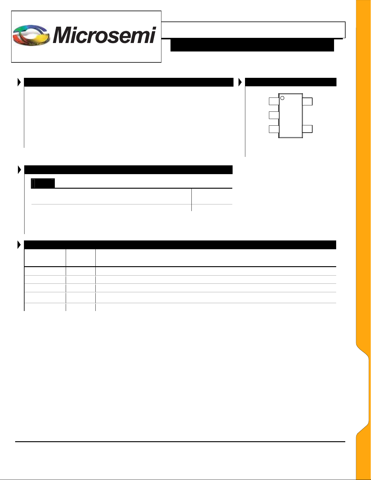
PACKAGE PIN OUT
+ 0.3V
IN
1
2
3
RoHS / Pb-free 100% Matte Tin Lead Finish
SE PACKAGE
(Top View)
WWW.Microsemi .COM
5
4
SE
Thermal Resistance – Junction to Ambient, θJA
Junction Temperature Calculation: TJ = TA + (PD x θJA).
The θ
system. All of the above assume no ambient airflow.
PIN NAME
VIN 1 Unregulated Input Supply Voltage
GND 2 Ground Pin
ENABLE 3 Enable Control Input, Enable High
ADJUST 4 Adjust Control Input for Resistor Divider Network.
VOUT 5 Regulated Output Voltage. Regulator stability is achieved with an external capacitor of 10µF.
5-PIN SOT-23 PACKAGE
Two – Layer Board
Four – Layer Board
numbers are guidelines for the thermal performance of the device/pc-board
JA
PIN
NUMBER
THERMAL DATA
FUNCTIONAL PIN DESCRIPTION
220°C/W
220°C/W
D
ESCRIPTION
Copyright © 2006
Rev. 1.0, 2006-04-07
Microsemi
Integrated Products Division
11861 Western Avenue, Garden Grove, CA. 92841, 714-898-8121, Fax: 714-893-2570
Page 2
P
P
A
A
C
C
K
K
A
A
G
G
E
E
D
D
A
A
T
T
A
A
LX8211A
TM
RECOMMENDED OPERATING CONDITIONS
®
Parameter Symbol
Input Operating Voltage Range (Note 1)
Minimum Output Voltage
Enable Input Voltage Range
Continuous Output Current Range I
Operating Temperature Range TJ -40 125 °C
Input Capacitor (VIN to GND) CIN 1.0 1.0* µF
Output Capacitor (V
Note 1: The minimum VIN has to meet two conditions V
* Size your output capacitor to meet the transient loading requirement. If you have a very dynamic load, a lower ESR and larger value capacitor will
improve the response to these load steps.
to GND) C
OUT
> 3.0V and V
IN
> V
IN
OUT
150mA Low Dropout Regulator
LX8211A
Min Typ Max
3.0 13.0 V
V
IN
2.3 V
ENABLE 0 VIN
0.1
150
+ V
OUT
10 µF
OUT
.
DROPOUT
Units
mA
Unless otherwise specified, the following specifications apply over the operating ambient temperature -40°C ≤ T
noted. Test conditions: V
methods.
Parameter Symbol Test Conditions
IN
= V
OUT
ELECTRICAL CHARACTERISTICS
+1V, V
= 2.9V; I
OUT
= 10mA; CIN = 1µF; C
OUT
OUT
≤ 125°C except where
J
= 10µF; TJ = TA, using low duty cycle pulse testing
LX8211A
Min Typ Max
Units
WWW.Microsemi .COM
Adjust Reference Voltage V
ΔV
Line Regulation
Load Regulation
Dropout Voltage
(Note2)
Ground Pin Current I
Adjust Input Bias Current I
Enable Pin Current IEN VEN = VIN 25 µA
Enable Threshold
Short Circuit Current Limit IOUTSC V
Power Supply Rejection Ratio PSRR TJ = 25°C, f = 120Hz 75 dB
Output Noise eN TJ = 25°C, C
Thermal Shutdown Temperature TSD 170 °C
Note 2: Dropout voltage is defined as the input to output differential at which the output voltage drops 1% below the nominal value.
Note 3: Limits require operation within recommended operating conditions.
⎛
⎜
⎝
ΔV
⎛
⎜
⎝
()
O
ΔV
O
IN
ΔI
O
VV −
OIN
⎞
⎟
⎠
⎞
⎟
⎠
Note 3 1.225 1.25 1.275 V
ADJ
VIN = V
V
RV
TJ = 25°C, I
V
RI
I
OUT
I
LOAD
I
V
LOAD
DO
I
LOAD
I
LOAD
Enable = Hi, I
Enable = Hi, I
GND
Enable = Low (Standby) 5 µA
Current Flows Out of Pin 4 50 500 nA
ADJ
VIH 2.0 V
0.18 V
V
IL
OUT
+ 1.0 TO 13 Volts, I
OUT
: 0.5 TO 150mA 0.05 0.2 %V
OUT
: 0.5 TO 150mA 0.5 %V
= 10mA, ΔVO = -1%
= 50mA, ΔVO = -1%
= 100mA, ΔVO = -1%
= 150mA, ΔVO = -1%
= 100mA 600 1500 µA
OUT
= 150mA 1300 2500 µA
OUT
= 0V 400 mA
= 10µF 260 nv /√Hz
OUT
=0.1mA 0.04 0.1 %/V
OUT
0.1 V
0.12 0.23 V
0.175 0.3 V
0.25 0.35 V
NOM
NOM
E
E
L
L
E
E
C
C
T
T
R
R
I
I
C
C
A
A
L
L
S
S
Copyright © 2006
Rev. 1.0, 2006-04-07
Microsemi
Integrated Products Division
11861 Western Avenue, Garden Grove, CA. 92841, 714-898-8121, Fax: 714-893-2570
Page 3

LX8211A
TM
V
IN
Thermal
Current
Limit
ENABLE
Shutdown
Control
Logic
®
BLOCK DIAGRAM
150mA Low Dropout Regulator
V
+
ADJUST
OUT
-
WWW.Microsemi .COM
VREF
GND
LX8211A
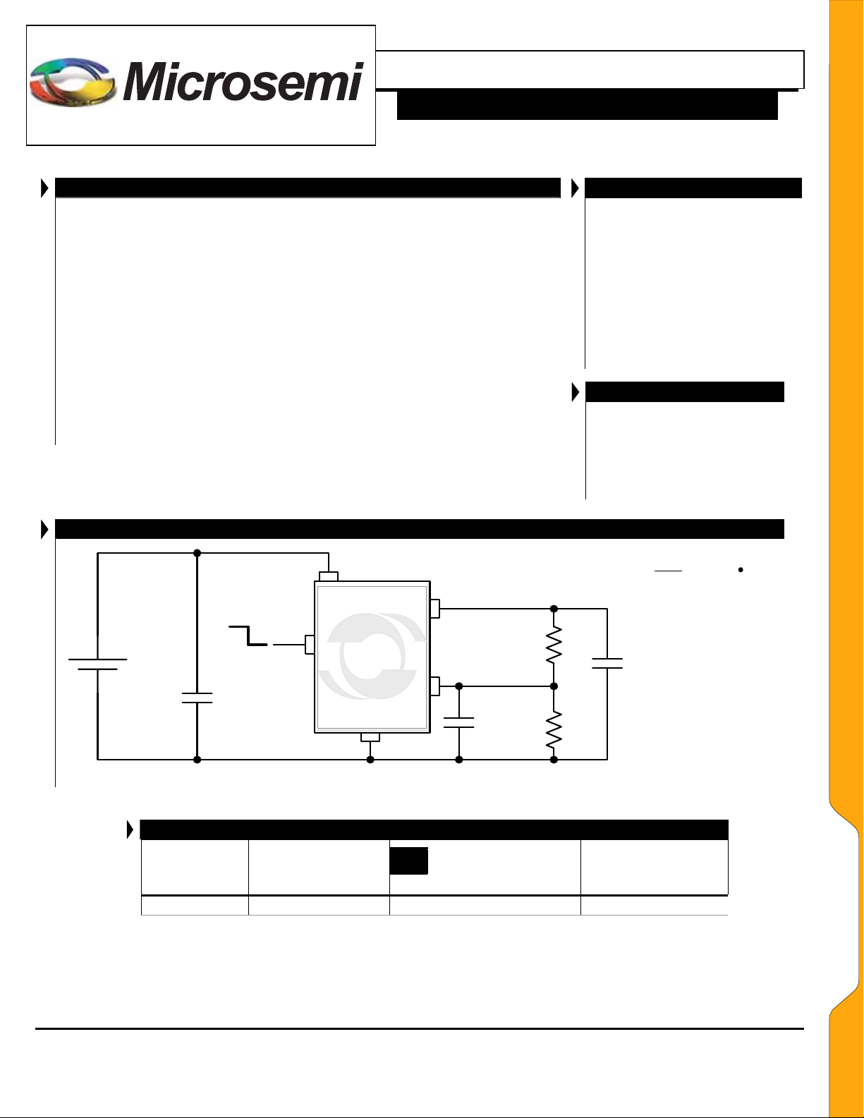
Figure 1 – Simplified Adjustable Version Block Diagram
B
B
L
L
O
O
C
C
K
K
D
D
I
I
A
A
G
G
R
R
A
A
M
M
Copyright © 2006
Rev. 1.0, 2006-04-07
Microsemi
Integrated Products Division
11861 Western Avenue, Garden Grove, CA. 92841, 714-898-8121, Fax: 714-893-2570
Page 4

LX8211A
TM
Typical performance characteristics, unless otherwise specified are: C
T
= 25°C, ENABLE is tied to VIN.
A
1.252
1.25
1.248
1.246
1.244
1.242
V ADJUST, Volts
1.24
1.238
-50 -25 0 25 50 75 100 125 150
300
250
200
150
100
50
DROPOUT VOLTAGE, mV
0
-50 -25 0 25 50 75 100 125 150
V ADJUST vs. TEMPERATURE
TEMPERATURE, °C
DROPOUT VOLTAGE (Vin=3.9V)
150mA
100mA
10mA
TEMPERATURE, °C
TYPICAL CHARACTERISTICS
GROUND CURRENT vs IOUT (Vin=3.9V)
2.25
2.00
1.75
1.50
1.25
1.00
CURRENT, mA
0.75
0.50
0.25
0
-50 -25 0 25 50 75 100 125 150
TEMPERATURE, °C
®
150mA
100mA
10mA
150mA Low Dropout Regulator
= 1µF, C
IN
2.915
2.91
2.905
2.9
2.895
2.89
V ADJUST, Volts
2.885
2.88
550
525
500
475
450
425
400
375
CURRENT, mA
350
325
300
-50 -25 0 25 50 75 100 125 150
0.30
0.25
0.20
0.15
0.10
VOUT, % CHANGE
0.05
0.00
= 10µF, CBY = 470pF, VIN = 4V, V
OUT
VOUT (Programmed to 2.9V) vs. TEMPERATURE
-50 -25 0 25 50 75 100 125 150
TEMPERATURE, °C
SHORT CIRCUIT CURRENT vs. TEMP and VIN
TEMPERATURE, °C
= 2.9V,
OUT
LINE and LOAD REGULATION
LINE (3.9-13v)
LOAD(0.5MA-150MA)
-50 -25 0 25 50 75 100 125 150
TEMPERATURE, °C
VIN=13V
VIN=3.9V
WWW.Microsemi .COM
C
C
H
H
A
A
R
R
T
T
S
S
Copyright © 2006
Rev. 1.0, 2006-04-07
Microsemi
Integrated Products Division
11861 Western Avenue, Garden Grove, CA. 92841, 714-898-8121, Fax: 714-893-2570
Page 5

LX8211A
TM
Typical performance characteristics, unless otherwise specified are: C
T
= 25°C, ENABLE is tied to VIN.
A
VIN = 4V, CIN = 1µF, C
CH2 = V
= 2.9V. CH1 - V
OUT
Enable Response
= 10µF, C
OUT
TYPICAL CHARACTERISTICS (CONTINUED)
Power Supply Rejection vs. Frequency
0
-10
-20
-30
-40
-50
-60
-70
-80
-90
-100
100 1K 10K 100K
ENABLE
= 470pF, I
BYP
= 100mA.
OUT
®
10MA LOAD C
150mA Low Dropout Regulator
= 1µF, C
IN
= 470PF
BYPASS
VIN = 4V, CIN = 1µF, C
CH2 = V
= 10µF, CBY = 470pF, VIN = 4V, V
OUT
Line Regulation Step Response
= 2.9V. CH1 = VIN from 3.5V to 4.5V
OUT
= 10µF, C
OUT
WWW.Microsemi .COM
= 2.9V,
OUT
= 470pF, I
BYP
= 100mA.
OUT
VIN = 4V, CIN = 1µF, C
CH2 = V
Copyright © 2006
Rev. 1.0, 2006-04-07
= 2.9V. CH4 = I
OUT
Load Transient Response
= 10µF, C
OUT
STEP
= 470pF, I
BYP
= 20mA to 70mA
OUT
= 50mA.
VIN = 4V, CIN = 1µF, C
CH2 = V
= 2.9V. CH4 = I
OUT
Load Transient Response
= 10µF, C
OUT
Microsemi
11861 Western Avenue, Garden Grove, CA. 92841, 714-898-8121, Fax: 714-893-2570
Integrated Products Division
= 470pF, STEP Load = 100mA.
BYP
= 20mA to 100mA
STEP
Page 6
C
C
H
H
A
A
R
R
T
T
S
S

LX8211A
p
p
TM
Description
The LX8211A is a family of LDO (Low Dropout) linear regulators in
a small SOT-23 Package, which provides a compact and cost effective
solution. The family includes several fixed output voltages, along with
an adjustable version. The internal PNP power device provides low
dropout regulation with fast line and load transient response. It also
includes internal current limit and thermal shutdown circuitry. This
section contains information about the selection of external capacitors,
thermal, and layout consideration.
APPLICATION INFORMATION
Input Capacitor
To improve load transient response and noise rejection a bypass
capacitor is recommended, but it is not required for stability. There are
no requirements for the ESR (Equivalent Series Resistor) on the input
capacitor, but tolerance and temperature coefficient must be
considered when selecting the capacitor to ensure the capacitor will be
around 1µF over the entire operating temperature range. For the
LX8211A connect a ceramic type capacitor (1µF) between VIN and
ground.
Output Capacitor
To maintain a constant output voltage a feedback loop is necessary.
The feedback loop causes a well known a phase shift, the amount of
phase shift determines the loop stability. Therefore the LX8211A, like
any low dropout regulator, requires an output capacitor with low ESR
(Equivalent Series Resistor) connected between V
stabilize the internal control loop. For the LX8211A a ceramic,
tantalum, or electrolytic capacitor with the minimum recommended
capacitance value at 10µF with ESR between 5mΩ and 1Ω will satisfy
the stability for whole operating range.
and GND to
OUT
Adjustable Output Voltage
The LX8211A-00 adjustable regulator’s output voltage can be
externally set by connecting the ADJ pin to an external resistor divider
(See Figure 1). The output voltage can be calculated using:
R2
⎤
⎡
11.25V
OUT
⎥
⎢
R1
⎦
⎣
[]
R2I
•++=
ADJ
Enable
The Enable pin allows the LX8211A to be turned on and off. The
Enable pin is compatible with standard TTL-CMOS levels. A logic
zero (0.4V) on the Enable pin shuts the LX8211A off and reduces the
supply current to less than 1µA. Pulling the Enable input high (2.0V)
causes normal operation to resume. If the Enable feature is not used,
this pin can be connected to V
Copyright © 2006
Rev. 1.0, 2006-04-07
.
IN
11861 Western Avenue, Garden Grove, CA. 92841, 714-898-8121, Fax: 714-893-2570
Integrated Products Division
®
Microsemi
150mA Low Dropout Regulator
Minimum Load Requirement
The LX8211A is stable even at zero load; no minimum load is required
for operation, which is especially important in keep-alive applications.
However line regulation is improved with a minimum load of 100µA.
Temperature Protection
Thermal protection shuts the LX8211A down when the junction
temperature exceeds approximately 150°C; there is no appreciable
thermal hysteresis.
Short Circuit Current Protection
The LX8211A includes over current protection, when the output load
current exceeds typically 400mA the circuit forces the regulator to
decrease in output.
Thermal Consideration
Thermal shutdown protects the integrated circuit from thermal
overload caused from a rise in junction temperature during power
dissipation. This means of protection is intended for fault protection
only and not as a means of current or power limiting during normal
application usage. Proper thermal evaluation should be done to ensure
that the junction temperature does not exceed its maximum rating.
Operating at the maximum TJ of 150°C can impact reliability. Due to
variation in individual device electrical characteristics and thermal
resistance, the built in thermal overload protection may be activated at
power levels slightly above or below the rated dissipation.
Power dissipation for regulator can be calculated using the following
equation:
PD = (V
(Note: power dissipation resulting from quiescent current is negligible)
For the SOT23 package, thermal resistance, θJA is 220°C/W when
mounted on a FR4 copper clad PCB. Junction temperature of the
integrated circuit can be calculated using:
TJ = TA + T
An example:
Given conditions: T
Calculated values:
Total Power dissipation
Junction Temperature
IN(MAX)-VOUT(MIN)
, substituting: T
RISE
Layout Consideration:
The layout must be done with low impedance paths for VIN, V
Ground by applying sufficient wide traces to avoid voltage drops and
ick up noise. Adding an area of PCB copper to the GND pin (pin2)
will reduce the overall
substrate. This will lower the device junction temperature improving
the overall output accuracy. The input / output capacitors must be
laced as close as possible to the voltage regulator output pin. To allow
the same voltage reference for all circuits, use a star configuration from
the output capacitor to the different loads.
) * I
OUT(MAX)
+ (PD * θJA).
A
= 60°C, VIN= 4.2V, V
A
P
= (4.2-2.7) V * 0.1A =0.15W
D(total)
T
= 60°C +(0.15W *220°C/W) = 93°C
J
θ
since it is thermally connected to the device
JA
= 2.7V, I
OUT
= 100mA.
OUT
, and
OUT
Page 7
WWW.Microsemi .COM
A
A
P
P
P
P
L
L
I
I
C
C
A
A
T
T
I
I
O
O
N
N

LX8211A
TM
SE
5 Pin Plastic SOT-23
®
PACKAGE DIMENSION
D
G
150mA Low Dropout Regulator
Dim
MILLIMETERS INCHES
MIN MAX MIN MAX
A 0.90 1.30 0.035 0.051
A1 0.90 1.45 0.035 0.057
B 0.25 0.50 0.010 0.020
H
E
C 0.09 0.20 0.004 0.008
D 2.80 3.10 0.110 0.122
E 1.50 1.75 0.059 0.069
F 0.95 BSC 0.038 BSC
G 1.90 BSC 0.075 BSC
H 2.60 3.00 0.102 0.118
I 0.35 0.55 0.014 0.022
A1
B
F
A
J
I
C
K
J 0.00 0.15 0.000 0.006
K 10° MAX 10° MAX
Note:
1. Dimensions do not include mold flash or protrusions;
these shall not exceed 0.155mm(.006”) on any side.
Lead dimension shall not include solder coverage.
WWW.Microsemi .COM
Copyright © 2006
Rev. 1.0, 2006-04-07
Microsemi
Integrated Products Division
11861 Western Avenue, Garden Grove, CA. 92841, 714-898-8121, Fax: 714-893-2570
Page 8
M
M
E
E
C
C
H
H
A
A
N
N
I
I
C
C
A
A
L
L
S
S

LX8211A
TM
®
NOTES
150mA Low Dropout Regulator
PRODUCTION DATA – Information contained in this document is proprietary to
Microsemi and is current as of publication date. This document may not be modified in
any way without the express written consent of Microsemi. Product processing does not
necessarily include testing of all parameters. Microsemi reserves the right to change the
configuration and performance of the product and to discontinue product at any time.
N
N
O
O
T
T
E
E
S
S
WWW.Microsemi .COM
Copyright © 2006
Rev. 1.0, 2006-04-07
Microsemi
Integrated Products Division
11861 Western Avenue, Garden Grove, CA. 92841, 714-898-8121, Fax: 714-893-2570
Page 9

 Loading...