Microsemi Corporation LX5225CDWP Datasheet

LIN DOC #:
5225
UltraMAX
ULTRA 18-LINE, PLUG AND PLAY SCSI TERMINATOR
T HE I NFINITE P OWER OF I NNOVATION
DESCRIPTION
The LX5225 SCSI terminator is part of Linfinity's
UltraMAX family of high-performance, adaptive, non-linear mode SCSI products, which are
designed to deliver true UltraSCSI performance
in SCSI applications. The low voltage BiCMOS
architecture employed in its design offers superior performance to older linear passive and
active techniques.
Linfinity's UltraMAX architecture employs
high-speed adaptive elements for each channel, thereby providing the fastest response
possible — typically 35MHz, which is 100 times
faster than the older linear regulator/terminator
approach used by other manufacturers. Products using this older linear regulator approach
have bandwidths which are dominated by the
output capacitor and which are limited to
500KHz (see further discussion in the Functional Description section). The UltraMAX
architecture also eliminates the output compensation capacitor typical in earlier terminator
designs. Each is approved for use with SCSI1, -2, -3, UltraSCSI and beyond — providing
the highest performance alternative available
today.
The LX5225 architecture is much more tolerant of marginal system integrations. A key
NOTE: For current data & package dimensions, visit our web site: http://www.linfinity.com.
improvement offered by the LX5225 lies in its
ability to ensure reliable, error-free communications even in systems which do not adhere
to recommended SCSI hardware design guidelines, such as the use of improper cable lengths
and impedances. Frequently, this situation is
not controlled by the peripheral or host designer and, when problems occur, they are the
first to be made aware of the problem.
To enter the disconnect mode, the disconnect pins must be driven low thereby disconnecting the LX5225 from the SCSI bus. The
LX5225 has two disconnect pins for SCSI Plug
and Play (PnP) applications. Quiescent current
is less than 150µA in this mode.
Reduced component counts is also inherent
in the LX5225 architecture. Traditional termination techniques require large stabilization
and transient protection capacitors of up to
20µF in value and size. The LX5225 architecture does not require these components, allowing all the cost savings associated with
inventory, board space, assembly, reliability,
and component costs.
The LX5225 is a superior pin-for-pin replacement for the LX5205 and the UCC5607.
TM
LX5225
P RODUCTION DATA SHEET
KEY FEATURES
■ SCSI Plug And Play, Dual Low Disconnect,
Logic Low Command Disconnects All
Ter mination Lines
■ Ultra-Fast Response For Fast-20 SCSI
Applications
■ 35MHz Channel Bandwidth
■ Sleep-Mode Current Less Than 150µA
■ NO External Compensation Capacitors
■ Compatible With Active Negation Drivers
■ Compatible With Passive And Active
Ter minations
■ Approved For Use With SCSI 1, 2, 3 And
Ultra SCSI
■ Hot Swap Compatible
■ Pin-For-Pin Compatible With LX5205 And
UC5607
DISC 1
DISC 2
PRODUCT HIGHLIGHT
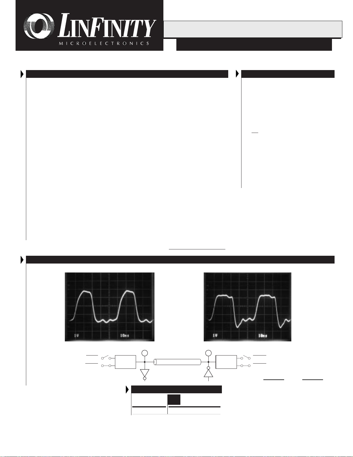
DRIVING WAVEFORM - 20MHZRECEIVING WAVEFORM - 20MHZ
Receiver
LX5225
1 Meter, AWG 28
PnP
LX5268 LX5268
PACKAGE ORDER INFO
T
(°C)
A
Plastic SOWB
DWP
28-pin, Power
0 to 70 LX5225CDWP
Note: All surface-mount packages are available in Tape & Reel.
Append the letter "T" to part number. (i.e. LX5225CDWPT)
Driver
LX5225
PnP
DISC 1
DISC 2
NOTE:
For An In-Depth
Discussion On Applying
SCSI, Request Linfinity
Application Note:
"Understanding The
Single-Ended SCSI Bus"
Copyright © 1999
Rev. 1.0 5/99
L INF INITY MICROELECTRONICS INC.
11861 WESTERN AVENUE, GARDEN GROVE, CA. 92841, 714-898-8121, FAX: 714-893-2570
1

PRODUCT DATABOOK 1996/1997
LX5225
ULTRA 18-LINE, PLUG AND PLAY SCSI TERMINATOR
RODUCTION DATA SHEET
P
ABSOLUTE MAXIMUM RATINGS (Note 1)
TermPwr Voltage .................................................................................................+7V
Signal Line Voltage ................................................................................... 0V to +7V
Operating Junction Temperature
Plastic (DWP Packages) ............................................................................... 150°C
Storage Temperature Range .............................................................. -65°C to 150°C
Lead Temperature (Soldering, 10 seconds) .................................................... 300°C
Note 1. Exceeding these ratings could cause damage to the device. All voltages are with
DWP PACKAGE:
Junction Temperature Calculation: TJ = TA + (P
The θ
system. All of the above assume no ambient airflow.
respect to Ground. Currents are positive into, negative out of the specified
terminal.
THERMAL DATA
D
θθ
θ
θθ
JL
x θ
θθ
θ
θθ
JA
).
JA
THERMAL RESISTANCE-JUNCTION TO LEADS,
THERMAL RESISTANCE-JUNCTION TO AMBIENT,
numbers are guidelines for the thermal performance of the device/pc-board
JA
18°C/W
40°C/W
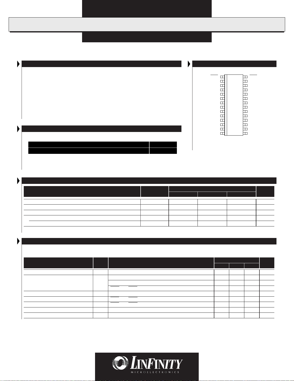
PACKAGE PIN OUTS
DISC1
T1
T2
T3
T4
HEAT SINK/GND
HEAT SINK/GND
T5
GND
T6
T7
T8
T9
V
TERM
DWP PACKAGE
(Top View)
UltraMAX
128
227
326
425
524
623
722
821
920
10 19
11 18
12 17
13 16
14 15
DISC2
T18
T17
T16
T15
T14
HEAT SINK/GND
HEAT SINK/GND
HEAT SINK/GND
T13
T12
T11
T10
N.C.
RECOMMENDED OPERATING CONDITIONS (Note 2)
Parameter
Termpwr Voltage V
Signal Line Voltage
Disconnect Input Voltage
Operating Virtual Junction Temperature Range
LX5225C
Note 2. Range over which the device is functional.
Symbol
TERM
Recommended Operating Conditions
Min. Typ. Max.
Units
4.0 5.5 V
05V
0V
TERM
V
0 125 °C
ELECTRICAL CHARACTERISTICS
Term Power = 4.75V unless otherwise specified. Unless otherwise specified, these specifications apply at the recommended operating ambient temperature of TA = 25°C. Low duty cycle pulse testing techniques are used which maintains junction and case temperatures equal to the ambient temperature.
Parameter
Symbol
Output High Voltage V
TermPwr Supply Current I
Output Current I
OUTVOUT
Disconnect Input Current I
Output Leakage Current I
Channel Bandwidth BW
Termination Sink Current, per Channel I
SINK
Test Conditions Units
OUT
All data lines = open
CC
All data lines = 0.2V
DISC1 and DISC2 Pins < 0.8V
= 0.2V
DISC1 and DISC2 Pins = 0V
IN
DISC1 and DISC2 Pins = < 0.8V, VO = 0.2V
OL
V
= 4V
OUT
LX5225
Min. Typ. Max.
2.65 2.85 V
10 15 mA
424 450 mA
50 150 µ A
-20 -22 -24 mA
-10 µA
1µA
35 MHz
7mA
2
Copyright © 1999
Rev. 1.0 5/99
 Loading...