Microsemi Corporation LX5107CDW, LX5107CPWP Datasheet

LIN DOC #:
5107
LX5107
9-LINE LOW CAPACITANCE, µPOWER SCSI TERMINATOR
THE INFINITE POWER OF INNOVATION
DESCRIPTION
The LX5107 is a nine-line active terminator
for the SCSI parallel bus. This SCSI standard recommends active termination at
both ends of the SCSI bus.
During disconnect mode, the LX5107
requires a meager 30µA of supply current
while offering only 3.0pF of output capacitance. To enter this low-power mode, the
disconnect pin should be driven low
thereby disconnecting the terminating resistors and placing the internal low dropout regulator into low-power mode. In
disconnect mode, each termination line
presents a high impedance to the SCSI bus
with the overall effect being to preserve
high signal integrity and yield subsequent
reliable, error free communications.
During normal operation, the LX5107
consumes only 600µA of current which is
IMPORTANT: For the most current data, consult LinFinity's web site: http://www.linfinity.com.
the lowest enabled supply current of any
terminator available on the market today.
Linfinity's proprietary BiCMOS low dropout regulator architecture enables this
unique and very efficient operating characteristic.
The LX5107 also offers a precisely
trimmed channel output current specified
to a 5% tolerance. The maximum value
of the output current is trimmed as closely
as possible to the SCSI standard maximum
specification to give the highest possible
noise margin for fast SCSI operation. In
addition, the LX5107 sinks up to 50mA of
current making it compatible with today's
fast active negation drivers.
The LX5107 is a superior, pin-for-pin
replacement for a variety of industry products such as the DS2107S and DS21S07A
PRODUCT HIGHLIGHT
P RODUCTION DATA SHEET
KEY FEATURES
■ 3.0pF OUTPUT CAPACITANCE DURING
DISCONNECT
■ 30µA SUPPLY CURRENT IN DISCONNECT
MODE
■ 600µA SUPPLY CURRENT DURING NORMAL
OPERATION
■ 50mA SINK CURRENT FOR ACTIVE
NEGATION
■ LOGIC COMMAND DISCONNECTS ALL
TERMINATION LINES
■ CURRENT LIMIT AND THERMAL PROTECTION
■ COMPATIBLE WITH SCSI 1, 2 AND 3
STANDARDS
■ MEETS SCSI HOT PLUGGING CAPABILITY
■ CONSULT FACTORY FOR APPLICATION TEST
REPORT: 5107TR
.
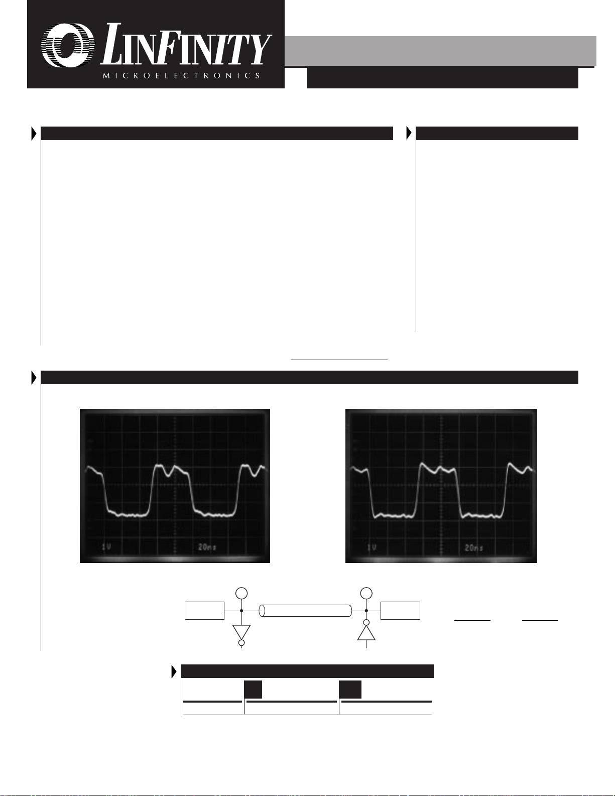
RECEIVING WAVEFORM - 10MHZ DRIVING WAVEFORM - 10MHZ
Receiver
1 Meter, AWG 28
LX5107 LX5107
LX5268 LX5268
PACKAGE ORDER INFORMATION
(°C)
T
J
0 to 70 LX5107CDW LX5107CPWP
Note: All surface-mount packages are available in Tape & Reel.
Append the letter "T" to part number. (i.e. LX5107CDWT)
Plastic SOWB
DW
16-pin
Driver
Plastic TSSOP
PWP
20-pin, Power
NOTE:
For An In-Depth
Discussion On Applying
SCSI, Request Linfinity
Application Note:
"Understanding The
Single-Ended SCSI Bus"
Copyright © 1997
Rev. 1.2 11/97
L INFINITY MICROELECTRONICS INC.
11861 WESTERN AVENUE, GARDEN GROVE, CA. 92841, 714-898-8121, FAX: 714-893-2570
1

LX5107
PRODUCT DATABOOK 1996/1997
9-LINE LOW CAPACITANCE, µPOWER SCSI TERMINATOR
RODUCTION DATA SHEET
P
ABSOLUTE MAXIMUM RATINGS (Note 1)
TermPwr Voltage .................................................................................................+7V
Signal Line Voltage ................................................................................... 0V to +7V
Regulator Output Current ................................................................................... 0.5A
Operating Junction Temperature
Plastic (DW, PW Packages) ......................................................................... 150°C
Storage Temperature Range .............................................................. -65°C to 150°C
Lead Temperature (Soldering, 10 seconds) .................................................... 300°C
Note 1. Exceeding these ratings could cause damage to the device. All voltages are with
respect to Ground. Currents are positive into, negative out of the specified
terminal.
THERMAL DATA
DW PACKAGE:
THERMAL RESISTANCE-JUNCTION TO AMBIENT,
θθ
θ
θθ
JA
95°C/W
PWP PACKAGE:
D
x θ
θθ
θ
θθ
JA
).
JA
THERMAL RESISTANCE-JUNCTION TO AMBIENT,
Junction Temperature Calculation: T
The θ
numbers are guidelines for the thermal performance of the device/pc-board
JA
system. All of the above assume no ambient airflow.
= TA + (P
J
83°C/W
POWER UP / POWER DOWN FUNCTION TABLE
Disconnect Outputs
L HI Z 30µA
H Enabled 600µA
Open Enabled 600µA
Quiescent
Current
PACKAGE PIN OUTS
V
V
GND
V
TERM
HS-GND
HS-GND
V
REF
GND
REF
R1
R2
R3
R4
R5
1 16
TERM
R1
215
R2
314
R3
413
R4
512
R5
611
1
710
89
DW PACKAGE
(Top View)
219
318
417
516
615
714
813
912
1
10 11
PWP PACKAGE
(Top View)
20
PD
V
REF
N.C.
R9
R8
R7
R6
V
TERM
PD
V
HS-GND
N.C.
R9
R8
R7
R6
HS-GND
V
2
REF
TERM
2
2
Copyright © 1997
Rev. 1.2 11/97
 Loading...