Microsemi Corporation LX1669CD Datasheet

LIN DOC #:
LX1669
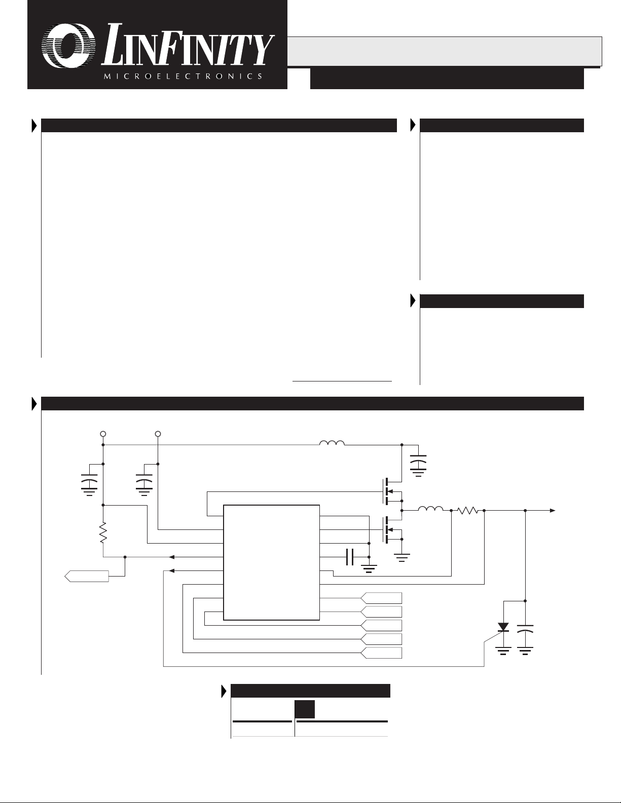
5V
CPU Core
V
CORE
C2
1500µFx3
Q1
IRL3102
Q2
IRL3303
L1
2.5µH
C1
1500µF x 6
R
SENSE
2.5m
Ω
C8
1µF
TDRV
V
CC12
V
CC5
PWRGD
OVP
VID0
VID1
VID2
PGND
BDRV
AGND
SS/EN
V
FB
V
CORE
VID4
VID3
8
VID3
VID4
VID2
VID1
VID0
C3
1µF
12V
7
6
5
4
3
2
1
11
12
13
14
15
16
9
10
L2,
1µH
Q4*
SCR
2N6504
R3
10k
Ω
C
SS
0.1µF
PWRGD
* Q4 optional OVP crowbar
1669
LX1669
P ROGRAMMABLE DC:DC CONTROLLER
T HE I NFINITE P OWER OF I NNOVATION
DESCRIPTION KEY FEATURES
The LX1669 is a Monolithic Switching
Regulator Controller IC designed to
provide a low cost, high performance
adjustable power supply for advanced
microprocessors and other applications
requiring a very fast transient response
and a high degree of accuracy. It provides
a programmable switching regulator output suitable for powering Pentium
®
II and
other processors.
Programmable Synchronous Recti-
fier Driver for CPU Core. The main
output is adjustable from 1.3 to 3.5V using
a TTL-compatible 5-bit digital code to
meet Intel specifications. The IC can read
the signal from a DIP-switch, hardwired to
Pentium II processor’s pins or from software. The 5-bit code adjusts the output
voltage between 1.30 and 2.05V in 50mV
increments, and between 2.0 and 3.5V in
NOTE: For current data & package dimensions, visit our web site: http://www.linfinity.com.
100mV increments. The device can drive
dual MOSFET’s resulting in typical efficiencies of 85 – 90%, even with loads in
excess of 10A.
Short-circuit Current Limiting with-
out Expensive Current Sense Resistors. The current sensing mechanism can
use a PCB trace resistance or the parasitic
resistance of the main inductor. For
applications requiring a high degree of
accuracy, a conventional sense resistor
can be used.
Ultra-Fast Transient Response Re-
duces System Cost. The fixed frequency
modulated off-time architecture results in
the fastest transient response for a given
inductor.
Small Package Size. The LX1669 is
available in an economical 16-pin narrow
body SOIC package.
P RODUCTION DATA SHEET
■ 5-Bit Programmable Output For CPU Core
Supply
■ Power Solution For Pentium II Processors
■ No Sense Resistor Required For Short-Circuit
Current Limiting
■ Soft-Start And Hiccup-Mode Current
Limiting Functions
■ Modulated Constant Off-Time Control
Mechanism For Fast Transient Response And
Simple System Design
■ Power Good Flag
■ Over-Voltage Pin Can Drive SCR Crowbar Or
Turn Off Signal Silver-Box Power Supply
■ Digital-Compatible Inputs (Including VID Pins)
APPLICATIONS
■ Socket 7 Processor Supplies
■ Pentium II Processor Supplies
■ Deschutes CPU & L2-Cache Memory
Supplies
■ Voltage Regulator Modules
■ General Purpose And Microprocessor
DC:DC Supplies
Copyright © 1999
Rev. 1.0 4/99
PRODUCT HIGHLIGHT
Note: All surface-mount packages are available in Tape & Reel, append the letter "T" to part number. (i.e. LX1669CDT)
L INF INITY MICROELECTRONICS INC.
11861 WESTERN AVENUE, GARDEN GROVE, CA. 92841, 714-898-8121, FAX: 714-893-2570
PACKAGE ORDER INFO
(°C)
T
A
0 to 70 LX1669CD
D
Plastic SOIC
16-pin
1

LX1669
PRODUCT DATABOOK 1996/1997
P ROGRAMMABLE DC:DC CONTROLLER
RODUCTION DATA SHEET
P
ABSOLUTE MAXIMUM RATINGS (Note 1 & 2)
12V Supply Voltage (V
5V Supply Voltage (V
Output Drive Peak Current Source (500ns)....................................................... 1.0A
) .................................................................................. 18V
CC12
) ....................................................................................... 7V
CC5
Output Drive Peak Current Sink (500ns) ........................................................... 1.0A
Input Voltage (SS, VID[0:4]) ................................................................... -0.3V to 6V
Operating Junction Temperature .................................................................... 150°C
Storage Temperature Range ........................................................... -65°C to +150°C
Lead Temperature (Soldering, 10 Seconds) .................................................... 300°C
Note 1. Exceeding these ratings could cause damage to the device. All voltages are with
Note 2. V
respect to Ground. Currents are positive into, negative out of the specified
terminal.
supply is used as input to internal low dropout regulator. Voltages above
CC3
3.3V will cause increased thermal dissipation in the package. Power dissipation
should be limited to keep junction temperature below maximum rating.
THERMAL DATA
D PACKAGE:
D
x θ
θθ
θ
θθ
JA
).
JA
120°C/W
THERMAL RESISTANCE-JUNCTION TO AMBIENT,
Junction Temperature Calculation: TJ = TA + (P
The θ
numbers are guidelines for the thermal performance of the device/pc-board
JA
system. All of the above assume no ambient airflow.
PACKAGE PIN OUTS
TDRV
V
CC12
V
PWRGD
OVP
VID0
VID1
VID2
1 16
215
314
CC5
413
512
611
710
89
D PACKAGE
(Top View)
PGND
BDRV
AGND
SS/ENABLE
V
FB
V
CORE
VID4
VID3
2
Copyright © 1999
Rev. 1.0 4/99

PRODUCT DATABOOK 1996/1997
P ROGRAMMABLE DC:DC CONTROLLER
P RODUCTION DATA SHEET
ELECTRICAL CHARACTERISTICS
(
Unless otherwise specified, 4.75V < V
Parameter
Reference & DAC
Initial Accuracy V
Cumulative Regulation Accuracy 1.3V ≤ V
Timing
Off Time OT V
Switching Frequency Freq V
Error Comparator / CS-
Input Bias Current I
E
Delay to Output Overdrive ≤ 5mV
C
Current Sense +
Input Resistance R
Pulse By Pulse Current Limit V
Current Sense Delay To Output Overdrive ≤ 5mV
Output Drivers
Drive Rise Time, Fall Time T
Drive High V
Drive Low V
UVLO and Soft-Start (SS)
V
Start-Up Threshold V
CC5
Hysteresis
SS Resistor R
SS Output Enable V
Hiccup Duty Cycle DC
Supply Current
V
Dynamic Supply Current I
CC12
Static Supply Current 12V I
5V I
Power Good / Over-Voltage Protection (OVP)
Threshold (V
Hysteresis
Power Good Voltage Low I
Over-Voltage Threshold (V
OVP Sourcing Current V
VID Pins
Low Input VILInternally pulled up to V
High Input V
< 5.25V and 10.8V < V
CC5
Symbol
(Less 40mV output adaptive positioning)
CORE
= 2.0V
CORE
= 1.3V to 3.5V
CORE
1.0V < VSS = VFB < 3.5V
FB
0V < VFB = V
CORE
CLP
CL = 3000pF
RF
DHISOURCE
DLISINK
STVCC12
SS
EN
HICCSS
CD
VCC12VSS
VCC5VSS
IH
= 20mA
> 3.9V
= 0.1µF, V
Out Freq = 200kHz, CL = 3000pF, Synch., VSS > 0.5V
< 0.5V
< 0.5V
CORE
(V
CORE
= 4mA
PWRGD
CORE
= 2.0V
OVP
≤ 3.5V
CORE
CORE
= 20mA
/ V
) V
SET
/ V
) V
SET
/ V
), V
SET
< 13.2V, 0°C ≤ TA ≤ 70°C. Test conditions: V
CC12
Test Conditions
< 3.5V
= 2.00V, F
DAC
rising, V
CORE
falling, V
CORE
rising
CORE
= 100Hz
REQ
OUT2
OUT2
thru 30k
CC5
, 1.3V ≤ V
≥ 2.0V
≥ 2.0V
≤ 3.5V, T
CORE
= 25°C
A
LX1669
= 5V, V
CC5
Min. Typ. Max.
-1 +1 %
-1.5 1.5 %
45 60 mV
10 11 V
3.9 4.2 4.6 V
0.4 0.5 V
108 110 111 %
90 91 92 %
110 117 125 %
35 60 mA
2.0 V
= 12V, T = 25°C.
CC12
LX1669
2.4 µs
250 kHz
-0.3 -1 µ A
100 ns
12 kΩ
100 ns
100 ns
0.1 0.2 V
0.10 V
18 kΩ
10 %
24 mA
69mA
13 18 mA
2%
0.5 0.7 V
0.8 V
)
Units
Copyright © 1999
Rev. 1.0 4/99
3

LX1669
PRODUCT DATABOOK 1996/1997
P ROGRAMMABLE DC:DC CONTROLLER
RODUCTION DATA SHEET
P
ELECTRICAL CHARACTERISTICS
Table 1 - Adaptive Transient Voltage Output (Output Voltage Setpoint — Typical)
Processor Pins
0 = Low, 1 = High
VID4 VID3 VID2 VID1 VID0
011111.34V 1.30V
011101.39V 1.35V
011011.44V 1.40V
011001.49V 1.45V
010111.54V 1.50V
010101.59V 1.55V
010011.64V 1.60V
010001.69V 1.65V
001111.74V 1.70V
001101.79V 1.75V
001011.84V 1.80V
001001.89V 1.85V
000111.94V 1.90V
000101.99V 1.95V
000012.04V 2.00V
000002.09V 2.05V
111112.04V 2.00V
111102.14V 2.10V
111012.24V 2.20V
111002.34V 2.30V
110112.44V 2.40V
110102.54V 2.50V
110012.64V 2.60V
110002.74V 2.70V
101112.84V 2.80V
101102.94V 2.90V
101013.04V 3.00V
101003.14V 3.10V
100113.24V 3.20V
100103.34V 3.30V
100013.44V 3.40V
100003.54V 3.50V
* Nominal = DAC setpoint voltage with no adaptive output voltage positioning.
Output Voltage (V
0.0A
Nominal Output* (V
SET
)
)
SET
Note:
Adaptive Transient Voltage Output
In order to improve transient response a 40mV offset is built into the voltage comparator. At high currents, the
peak output voltage will be lower than the nominal set point , as shown in Figure 4. The actual output voltage
will be a function of the sense resistor, output current and output ripple.
4
Copyright © 1999
Rev. 1.0 4/99

PRODUCT DATABOOK 1996/1997
V
P ROGRAMMABLE DC:DC CONTROLLER
P RODUCTION DATA SHEET
CHARACTERISTICS CURVES
LX1669
100
95
90
85
EFFICIENCY (%)__
80
EFFICIENCY A T 3. 1V
EFFICIENCY A T 2. 8V
75
70
123456 7891011121314
EFFICIENCY A T 1. 8V
I
OUT
(A)
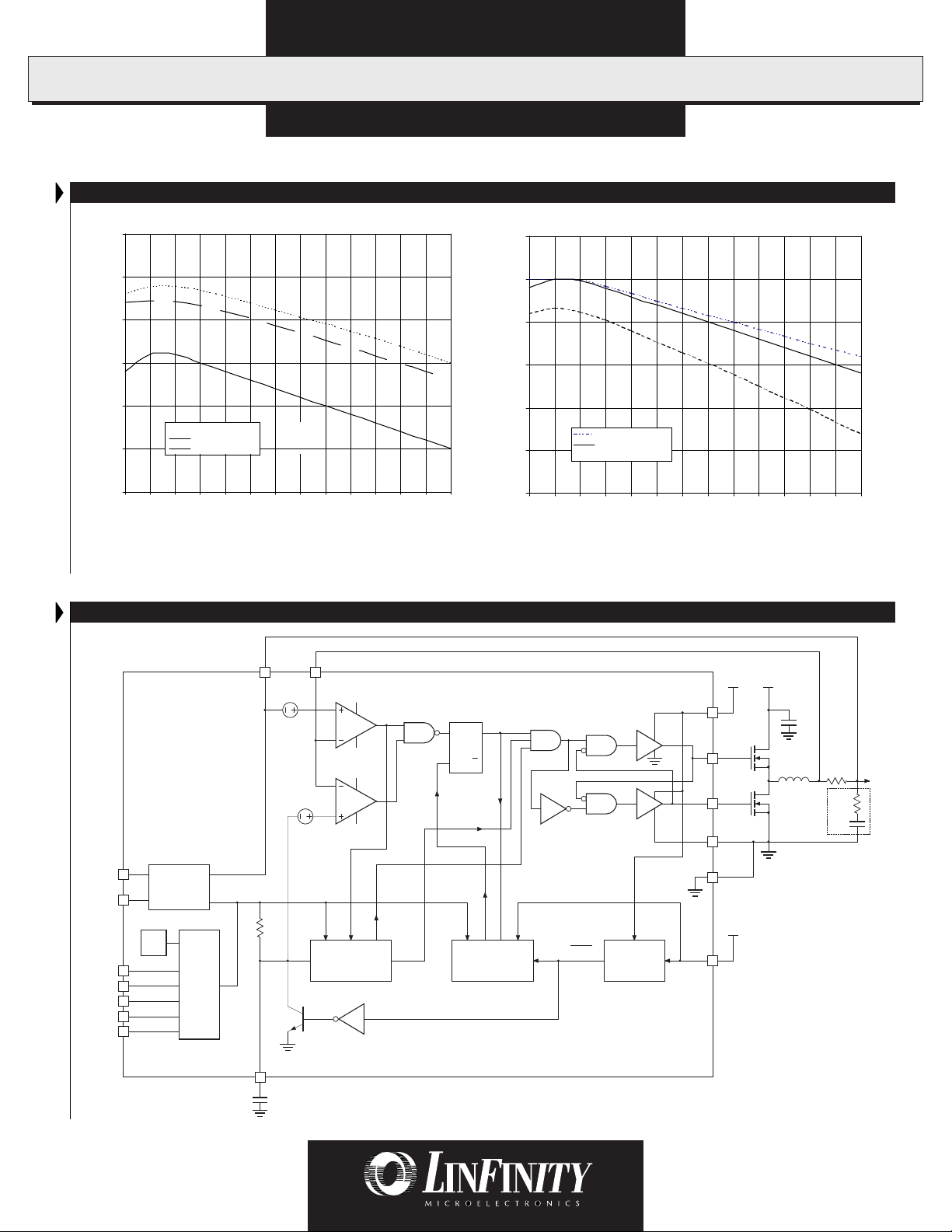
FIGURE 1 — Efficiency Test Results:
V
FB
CS Comp
Error Comp
Hiccup
= 5V
IN
I
PWRGD
OVP
ID[0:4]
Non-Synchronous Operation, V
4
Power Good
& OVP
5
V
REF
6
7
8
9
10
DAC
V
SET
V
CORE
R
20k
12
60mV
40mV
SS
11
100
95
90
85
EFFICIENCY (%)__
80
75
70
BLOCK DIAGRAM
RESET
V
RESET
Hiccup
R
SQ
Set
PWM
Q
Off-Time
Control
EFFICIENCY AT 3.1V
EFFICIENCY A T 2.8V
EFFICIENCY A T 1.8V
1234567891011121314
I
(A)
OUT
FIGURE 2 — Efficiency Test Results:
Synchronous Operation, VIN = 5V
+12V
VIN (5V)
2
V
UVLO
UVLO
15
16
14
1
3
CC12
TDRV
BDRV
PGND
AGND
+5V
V
CC5
C
IN
R
SENSE
L
V
ESR
C
OUT
CORE
SS/ENABLE
Copyright © 1999
Rev. 1.0 4/99
13
C
SS
FIGURE 3 — Block Diagram
5
 Loading...