Microsemi Corporation LX1571MY, LX1571IM, LX1571IDM, LX1571CM, LX1571CDM Datasheet
...
PACKAGE ORDER INFORMATION
T
A
(°C)
Plastic DIP
8-pin
0 to 70 LX157xCM LX157xCDM —
-40 to 85 LX157xIM LX157xIDM —
-55 to 125 — — LX157xMY
M
Plastic SOIC
8-pin
DM
Ceramic DIP
8-pin
Y
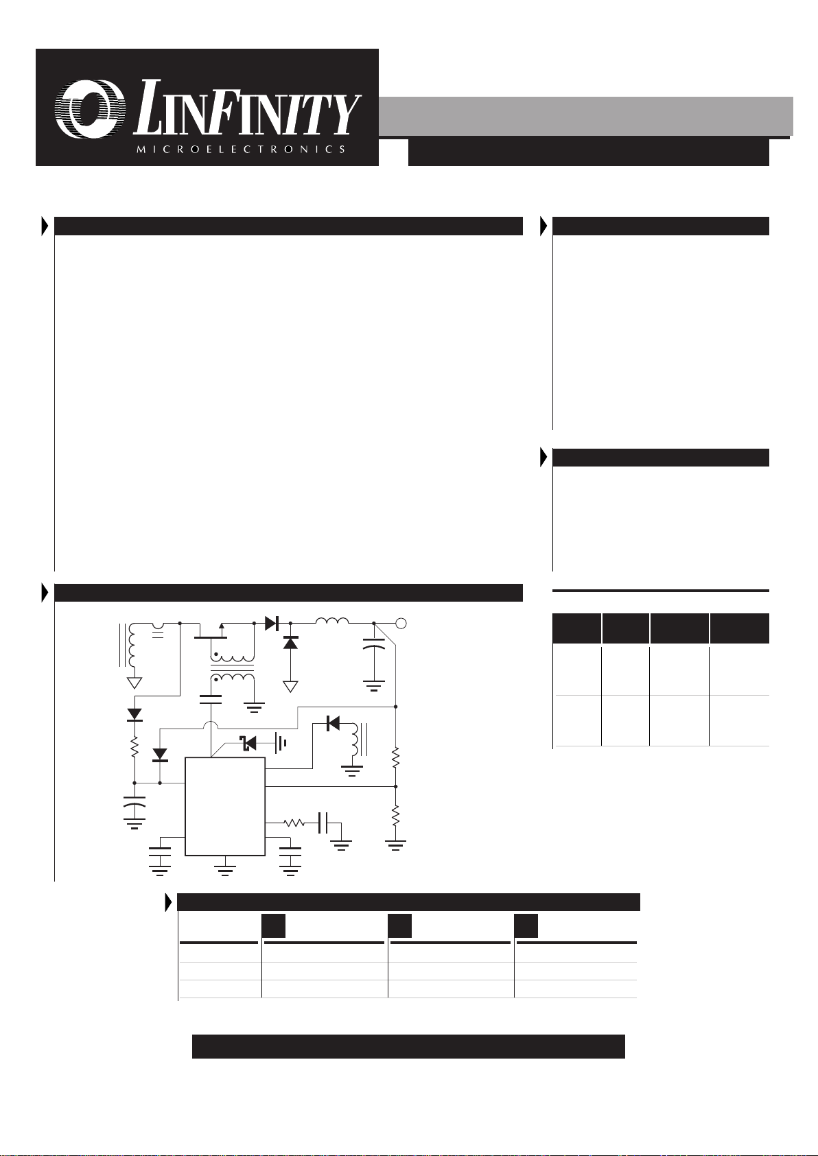
DESCRIPTION KEY FEATURES
p REPLACES COSTLY MAG-AMP CORES WITH
A LOW ON-RESISTANCE MOSFET
p LOOK-AHEAD SWITCHING
TM
ENSURES
SWITCH TURN ON BEFORE THE AC INPUT
TO ACHIEVE 100% ENERGY TRANSFER
p LOWER OVERALL SYSTEM COST
p LOWER PEAK CURRENT STRESS ON THE
PRIMARY SWITCH
p ALLOWS HIGHER OPERATING FREQUENCY
AND SMALLER OUTPUT INDUCTOR
p EASY SHORT-CIRCUIT PROTECTION
p CURRENT MODE APPROACH ACHIEVES
EXCELLENT DYNAMIC RESPONSE
The LX1570/71 series of controller ICs are
designed to provide all control functions in
a secondary-side regulator for isolated auxiliary or secondary power supplies. Auxiliary
or secondary-side controllers are used in a
variety of applications including multiple
output off-line power supplies, commonly
found in desktop computers, as well as telecommunications applications. Although they
can be used in all secondary output applications requiring precision regulation, they are
mainly optimized for outputs delivering more
than 3A current where standard three-terminal regulators lack the desired efficiency. For
these applications, the Mag Amp regulators
have traditionally been used. However, Mag
Amps have several disadvantages. First, because they have to withstand the maximum
input voltage during a short-circuit condition,
they are "over designed", typically by 2 times,
increasing the cost and size of the power
supply. Second, Mag Amps are inherently
leading edge modulators, so they can only
approach a certain maximum duty cycle, limited by the minimum delay and the magnetic BH loop characteristic of the Mag Amp
core. This forces an increase in the size of
the main transformer as well as the output
inductor, resulting in higher overall system
cost. The LX1570/71 eliminates all the
disadvantages of the Mag Amp approach
as well as improving system performance and reducing overall system cost.
The LX1570/71 is a current mode controller IC that controls the duty cycle of a switch
in series with the secondary AC output of
the power transformer in buck-derived applications, such as forward or bridge topologies. It offers features such as 100% duty
cycle operation for maximum energy transfer, pulse-by-pulse and hiccup current limiting with long off-time between the cycles
for reduced power dissipation, high-frequency operation for smaller magnetics, softstart, and current mode control for excellent dynamic response.
PRODUCT HIGHLIGHT
APPLICATIONS
■ SECONDARY-SIDE REGULATOR IN OFF-LINE
POWER SUPPLIES
■ COMPUTER POWER SUPPLIES, 3.3V OUTPUT
FOR NEW LOW-VOLTAGE PROCESSORS
AND MEMORIES
■ TELECOMMUNICATION AND MILITARY
DC/DC CONVERTERS
LX1571
V
CC
OUT
DRV
C.S.
V
FB
COMP
S.S.
GND
C
T
Aux Outpu
t
12V/8A
P
HASE MODULATED
AC S
YNCHRONOUS SECONDARY-SIDE CONTROLLER
P RELIMINARY DATA SHEET
THE INFINITE POWER OF INNOVATION
Copyright © 1997
Rev. 0.9.3 1/97
FOR FURTHER INFORMATION CALL (714) 898-8121
11861 WESTERN AVENUE, GARDEN GROVE, CA. 92841
LX1570/1571
LIN DOC #:
1570
1
P
ATENT PENDING
Note: All surface-mount packages are available in Tape & Reel.
Append the letter "T" to part number. (i.e. LX157xCDMT)
A VAILABLE OPTIONS PER PART #
Part #
C.L. C.S.
Application
Threshold
Option
Resistive
Output
LX1570 -0.2V
Sensing
Currents
< 4A
Current Output
LX1571 1V
Transformer
Currents
Sensing > 4A

P
HASE MODULATED
AC S
YNCHRONOUS SECONDARY-SIDE CONTROLLER
LX1570/1571
PRODUCT DATABOOK 1996/1997
Copyright © 1997
Rev. 0.9.3 1/97
2
P
RELIMINARY DAT A SHEET
ABSOLUTE MAXIMUM RATINGS (Note 1)
Supply Voltage (VCC) .................................................................................................... 40V
Digital Inputs ....................................................................................................... -0.3 to 7V
Output Peak Current Source (500nS) ........................................................................... 1A
Output Peak Current Sink (500nS)................................................................................ 1A
PACKAGE PIN OUTS
C
T
V
CC
OUT DRV
GND
S.S.
V
FB
COMP
C.S.
1 8
27
36
45
M & Y PACKAGE
(Top View)
DM PACKAGE
(Top View)
C
T
V
CC
OUT DRV
GND
S.S.
V
FB
COMP
C.S.
1 8
27
36
45
Note 1. Exceeding these ratings could cause damage to the device. All voltages are with respect
to Ground. Currents are positive into, negative out of the specified terminal.
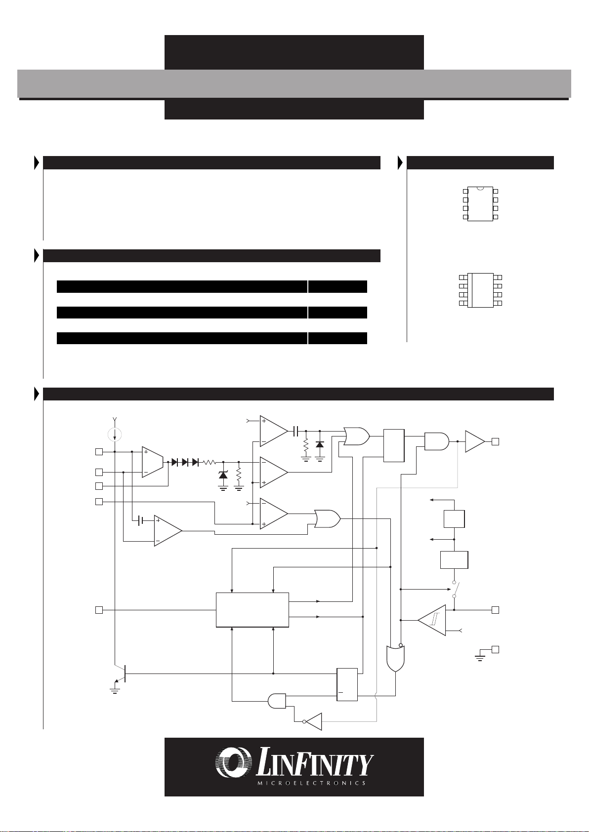
LX1571 BLOCK DIAGRAM
THERMAL DATA
M PACKAGE:
THERMAL RESISTANCE-JUNCTION TO AMBIENT,
θθ
θθ
θ
JA
95°C/W
DM PACKAGE:
THERMAL RESISTANCE-JUNCTION TO AMBIENT,
θθ
θθ
θ
JA
165°C/W
Y PACKAGE:
THERMAL RESISTANCE-JUNCTION TO AMBIENT,
θθ
θθ
θ
JA
130°C/W
Junction Temperature Calculation: T
J
= TA + (P
D
x θ
JA
).
The θ
JA
numbers are guidelines for the thermal performance of the device/pc-board system.
All of the above assume no ambient airflow.
Error Amp
Voltage Hiccup
Comp.
2.5V
Minimum
Current Comp
C.S. Comp
Current Mode
Hiccup Comp
RSQ
PWM Latch
7
6
5
GND
V
CC
OUT DRV
6V
RSQQ
Hiccup
Latch
2R
R
Internal
Bias
2.5V
REF
1V
5V
2.5V
16V
1.5V
0.25V
0.5V
4
3
2
1
S.S.
V
FB
C
OMP
C.S.
8
C
T
Voltage Mode Hiccup
Timing / Duty Cycle
Control
CHG
CONTROL
QUICK
CHG
CONTROL
LATCH RESET
CONTROL
LATCH
SET CONTROL
VALLEY
THRESHOLD
CONTROL
DISCH
CONTROL

P
HASE MODULATED
AC S
YNCHRONOUS SECONDARY-SIDE CONTROLLER
LX1570/1571
PRODUCT DATABOOK 1996/1997
3
Copyright © 1997
Rev. 0.9.3 1/97
P RELIMINARY DATA SHEET
Input Range LX1570 V
CSI
LX1571
Input Current LX1570 I
CSB
LX1571
C.S. Amplifier Gain LX1570 A
CS
LX1571
Minimum Current Threshold Voltage LX1570 V
CSMIN
LX1571
C.S. Delay to Driver Output 10% Overdrive
C.L. Pulse-By-Pulse Threshold Voltage LX1570 V
CLP
LX1571
C.L. Hiccup Threshold Voltage LX1570 V
CLH
LX1571
Voltage Hiccup Threshold V
HCCP
Initial Accuracy fOCT = , TJ = 25°C, measured at pin 6
Over Temp, measured at pin 6
Line Voltage Stability ∆f
OL
Charging Current I
CHG
Discharging Current I
DISCH
Leakage Current I
LK
C.S.
INPUT
= 1.5V
Ramp PK to PK V
RPP
C.S.
INPUT
= 0V
C.S.
INPUT
= 1.5V (1571), C.S.
INPUT
= -0.4V (1570)
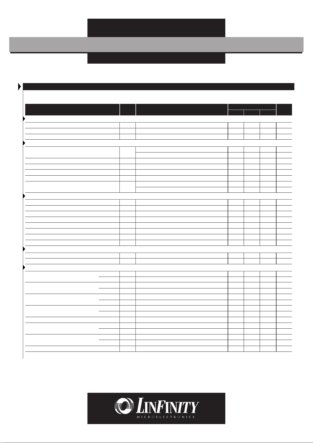
ELECTRICAL CHARACTERISTICS
Reference Section
Parameter
Symbol
Test Conditions
Initial Accuracy VRITA = 25ºC, measured at F.B pin
Line Regulation ∆V
RL
11V < VCC < 25
Temp Stability ∆V
RT
Note 2
Units
LX1570/1571
Min. Typ. Max.
2.475 2.500 2.525 V
±1 %
±1.5 %
Timing Section
90 100 110 kHz
85 100 115 kHz
±1 %
3mA
3.5 mA
4µA
0.6 V
6V
Error Amp / Soft Start Comp Section
Transconductance g
m
Input Bias Current I
B
Open Loop Gain A
VOL
Output Sink Current I
EA(SINK)VFB
= 2.6V
Output Source Current I
EA(SOURCE)VFB
= 2.4V
Output HI Voltage V
COMP-HI
Output LO Voltage V
COMP-LO
Slew Rate S
0.005 µΩ
0.1 1 µ A
60 70 dB
200 400 µA
200 400 µA
5.1 V
0.8 V
1 V/µSec
(Unless otherwise specified, these specifications apply over the ranges TA = -55 to 125ºC for the LX1570M/1571M, TA = -40 to 85ºC for the
LX1570I/1571I, and T
A
= 0 to 70ºC for LX1570C/1571C. VCC = 15V. Typ. number represents TA = 25ºC value.)
Soft-Start Section
Soft Start Timing Factor K
SS
Soft Start Discharge Current I
SS-DIS
35 50 65 ms/µF
TBD mA
Current Sense Section
-0.8 V
-0.3 6 V
25 µA
1µA
-13.5 -15 -16.5 V/V
2.7 3 3.3 V/V
-50 mV
250 mV
100 200 ns
-0.18 -0.2 -0.22 V
0.9 1 1.1 V
-0.3 V
1.5 V
2V
Note 2. Although this parameter is guaranteed, it is not 100% tested in production.

P
HASE MODULATED
AC S
YNCHRONOUS SECONDARY-SIDE CONTROLLER
LX1570/1571
PRODUCT DATABOOK 1996/1997
Copyright © 1997
Rev. 0.9.3 1/97
4
P
RELIMINARY DAT A SHEET
S.S. 1
V
FB
2
COMP 3
C.S. 4
GND 5
OUT 6
DRV
V
CC
7
C
T
8
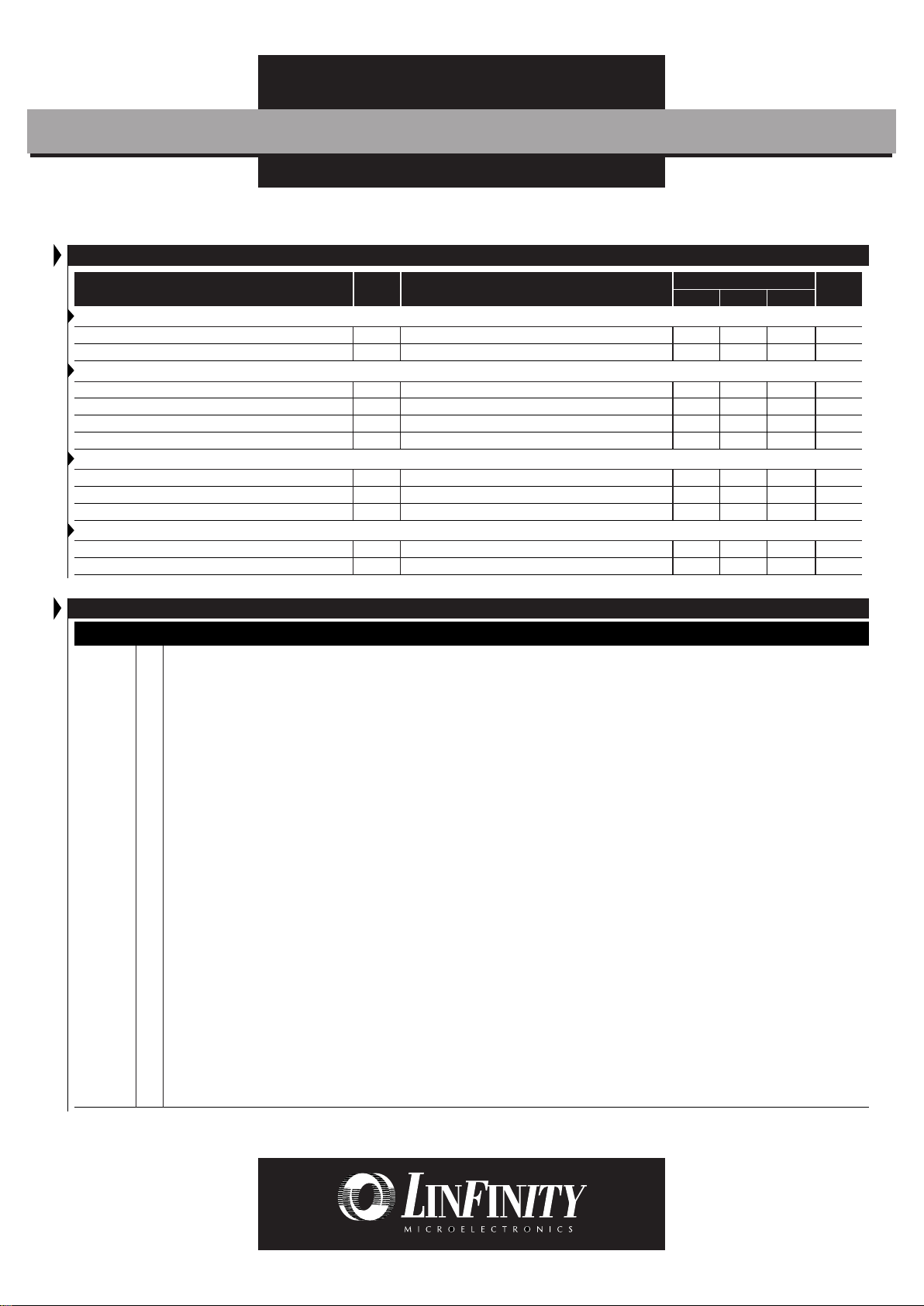
This pin acts as the soft-start pin. A capacitor connected from this pin to GND allows slow ramp up of the NI input
resulting in output soft start during start up. This pin is clamped to the internal voltage reference during the normal
operation and sets the reference for the feedback regulator.
This pin is the inverting input of the Error Amplifier. It is normally connected to the switching power supply output
through a resistor divider to program the power supply voltage. This pin instead of the NI pin is internally trimed to
1% tolerance to include the offset voltage error of the error amp.
This pin is the Error Amplifier output and is made available for loop compensation. Typically a series R&C network
is connected from this pin to GND.
A voltage proportional to the inductor current is sensed by an external sense resistor (1570) or current transformer (1571)
in series with the return line and is connected to this pin. The output drive is terminated and latched off when this voltage
amplified by the internal gain (see option table) exceeds the voltage set by the E.A output voltage. The maximum
allowable voltage at this pin during normal operation is -0.8V typ for LX1570 and 6V typ for LX1571.
This pin is combined control circuitry and power GND. All other pins must be positive with respect to this pin, except
for C.S pin.
This pin drives a gate drive transformer which drives the power mosfet. A Schottky diode such as 1N5817 must be
connected from this pin to GND in order to prevent the substrate diode conduction.
This pin is the positive supply voltage for the control IC. A high frequency capacitor must be closely placed and
connected from this pin to GND to provide the turn-on and turn-off peak currents required for fast switching of the power
Mosfet.
The free running oscillator frequency is programmed by connecting a capacitor from this pin to GND.
Pin # Description
FUNCTIONAL PIN DESCRIPTIONFUNCTIONAL PIN DESCRIPTION
FUNCTIONAL PIN DESCRIPTIONFUNCTIONAL PIN DESCRIPTION
FUNCTIONAL PIN DESCRIPTION
Rise / Fall Time tR / tFCL = 1000pF
Output HI V
DHISOURCE
= 200mA, VCS = 0V, VFB = 2.3V
Output LO V
DLISINK
= 200mA, VCS = 1.2V, VFB = 2.3V
Output Pull Down V
DPDVCC
= 0V, I
PULL UP
= 2mA
ELECTRICAL CHARACTERISTICS (Con't.)
Parameter
Symbol
Test Conditions Units
LX1570/1571
Min. Typ. Max.
1.7 2.0 2.4 V
52 54 56 %
E.A. Output to PWM Drive Offset V
OFS
Fixed Duty Cycle D
UVLO Section
15 16 17 V
91011V
5.5 6 6.5 V
Start-Up Threshold V
ST
Turn Off Threshold V
OFF
Hysterises V
H
Supply Current Section
Dynamic Operating Current I
Qd
Out Freq = 100kHz, CL = 0
Start-Up Current I
ST
18 30 mA
150 250 µA
50 ns
13.5 V
0.8 V
1V
PWM Section
Output Drive Section
 Loading...