

Page 1
A
LIN DOC #:
1562
LX1562/1563
S ECOND-GENERATION POWER FACTOR CONTROLLER
THE INFINITE POWER OF INNOVATION
DESCRIPTION KEY FEATURES
The LX1562 is a second-generation
family of power factor correction
controllers using a discontinuous mode
of operation. They are optimized for
electronic ballast applications. Many
improvements have been made over
the original SG3561A controller
introduced by Silicon General Semiconductor in 1992.
New features include the addition of
an internal start-up circuit eliminating
bulky external components while
allowing independent boost converter
operation. Addition of internal current
sense blanking eliminating the need for
an external R/C filter network. Internal
clamping of the error amplifier and
multiplier outputs improves turn on
overshoot characteristics and current
limiting. Special circuitry has also been
added to prevent no load runaway
conditions. And finally, output drive
clamps limiting power MOSFET gate
drive independent of supply voltage
greatly enhance the products practical
application.
Although the IC design has been
optimized for electronic ballast applications, it can also be used for power
factor correction in lower power (typ <
300W) AC-DC converters. One unique
feature of the device is encompassed
by the addition of internal logic
circuitry to detect zero crossing of the
inductor current thus maintaining the
discontinuous current mode of operation. This feature prevents large
current gaps from appearing thereby
minimizing distortion and enhancing
power factor correction.
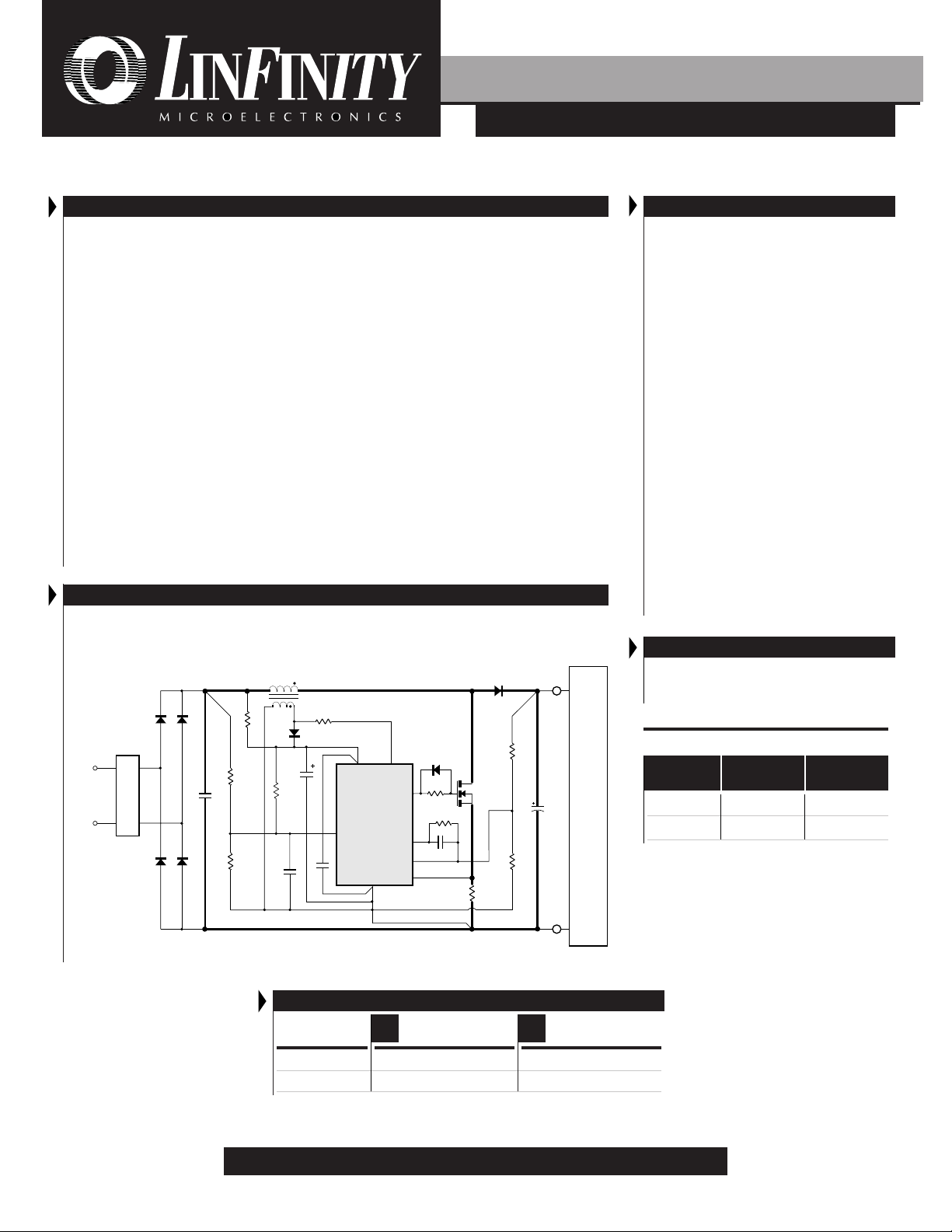
PRODUCT HIGHLIGHT
TYPICAL APPLICATION OF THE LX1562 IN AN 80W
F
LUORESCENT LAMP BALLAST WITH ACTIVE POWER FACTOR CONTROL
450µH
61T #22AWG
L1
AC-
C+
120V
AC
D1 D3
EMI FILTER
D2
1N4004
1N4004
1N4004
1N4004
100k
½W
R3
2.2M
R1
1%
1µF
C1
250V
D4
29k
R2
1%
C4
.01µF
7T
D5
22µF
R10
4.7M
1N4935
C2
C3
R4
22k
0.1µF
3
VINI
MULT
IN
8
DET
COMP
LX1562
GND
6
5
OUT
INV
C.S.
1N4148
7
2
1
4
D6
47
Ω
R5
R9 620k
C5
0.1µF
1/4W
P RODUCTION DATA SHEET
■■
■ INTERNAL START-UP CIRCUIT
■■
■■
■ INTERNAL CURRENT SENSE BLANKING
■■
■■
■ IMPROVED MICROPOWER START-UP
■■
CURRENT (300µA max.)
■■
■ CLAMPED E.A. OUTPUT FOR LOWER
■■
TURN-ON OVERSHOOT
■■
■ MULTIPLIER CLAMP LIMITS MAXIMUM
■■
INPUT CURRENT
■■
■ INTERNAL OVERVOLTAGE PROTECTION
■■
REPLACES BUILT-IN C.S. OFFSET
■■
■ PWM OUTPUT CLAMP LIMITS MOSFET
■■
GATE DRIVE VOLTAGE
■■
■ INCREASED UVLO HYSTERESIS REDUCES
■■
START-UP TIMING (LX1562 only)
■ LOW OPERATING CURRENT CONSUMPTION
■ INTERNAL 1.5% REFERENCE
■ TOTEM POLE OUTPUT STAGE
■ AUTOMATIC CURRENT LIMITING OF BOOST
STAGE
■ DISCONTINUOUS MODE OF OPERATION
WITH NO CURRENT GAPS
■ NO SLOPE COMPENSATION REQUIRED
APPLICATIONS
V
BOOST
MR854
230V
D7
1M
Ω
R7
1%
Q1
1RF730
11k
1%
3x
R6
1.3
Ω
C6
100µF
400V
R8
FLOURESCENT LAMP BALLAST
■■
■ ELECTRONIC BALLAST
■■
■ SWITCHING POWER SUPPLIES
A VAILABLE OPTIONS PER PART #
Part # Start-Up Hysteresis
LX1562 13.1V 5.2V
LX1563 9.8V 2.1V
Voltage Voltage
Note: Thick trace on schematic shows high-frequency, high-current path in circuit.
Lead lengths must be minimized to avoid high-frequency noise problems.
PACKAGE ORDER INFORMATION
T
(°C)
A
0 to 100 LX1562IM LX1562IDM
Plastic DIP
M
8-pin
Plastic SOIC
DM
8-pin
0 to 100 LX1563IM LX1563IDM
Note: All surface-mount packages are available in Tape & Reel.
Append the letter "T" to part number. (i.e. LX1562IDMT)
FOR FURTHER INFORMATION CALL (714) 898-8121
Copyright © 1996
Rev. 1.3 12/96
11861 WESTERN AVENUE, GARDEN GROVE, CA. 92841
1
Page 2

LX1562/1563
PRODUCT DATABOOK 1996/1997
S ECOND-GENERATION POWER FACTOR CONTROLLER
RODUCTION DATA SHEET
P
ABSOLUTE MAXIMUM RATINGS (Note 1)
Supply Voltage (VIN) ...................................................................................... -0.3V to 28V
Peak Driver Output Current (Note 3) ................................................................. ±500mA
Driver Output Clamping Diodes
V
> VCC or VO < -0.3V ........................................................................................ ±10mA
O
Detector Clamping Diodes
> 6V or V
V
DET
Error Amp, Multiplier, and Comparator Input Voltages ................................ -0.3V to 6V
< 0.9V ..................................................................................... ±10mA
DET
Detector Input Voltage (Note 2) ....................................................................... -0.3 to 6V
Operating Junction Temperature
Plastic (M and DM Packages) ............................................................................... 150°C
Storage Temperature Range ...................................................................... -65°C to 150°C
Lead Temperature (Soldering, 10 Seconds) ............................................................ 300°C
Note 1. Values beyond which damage may occur. All voltages are specified with respect to
ground, and all currents are positive into the specified terminal.
Note 2. With no limiting resistor.
Note 3. Current duty cycle is chosen such that T
is below 150°C.
J
THERMAL DATA
M PACKAGE:
THERMAL RESISTANCE-JUNCTION TO AMBIENT,
θθ
θ
θθ
JA
DM PACKAGE:
D
θθ
θ
θθ
x θ
JA
).
JA
THERMAL RESISTANCE-JUNCTION TO AMBIENT,
Junction Temperature Calculation: TJ = TA + (P
numbers are guidelines for the thermal performance of the device/pc-board system.
The θ
JA
All of the above assume no ambient airflow
95°C/W
165°C/W
PACKAGE PIN OUTS
E.A. INV.
E.A. OUT
MULT. INPUT
E.A. INV.
E.A. OUT
MULT. INPUT
C.S.
1 8
27
36
45
C.S.
M PACKAGE
(Top View)
1 8
27
36
45
DM PACKAGE
(Top View)
V
OUT
GROUND
I
IN
DET
V
IN
OUT
GROUND
I
DET
2
Copyright © 1996
Rev. 1.3 12/96
Page 3
PRODUCT DATABOOK 1996/1997
LX1562/1563
S ECOND-GENERATION POWER FACTOR CONTROLLER
P RODUCTION DATA SHEET
RECOMMENDED OPERATING CONDITIONS (Note 4)
Parameter
Symbol
Supply Voltage Range
Peak Driver Output Current
Operating Ambient Temperature Range:
LX1562/1563
Note 4. Range over which the device is functional.
ELECTRICAL CHARACTERISTICS
(Unless otherwise specified, these specifications apply over the operating ambient temperatures for the LX1562/1563 with 0°C ≤ TA ≤ 100°C; V
testing techniques are used which maintains junction and case temperatures equal to the ambient temperature.)
Parameter
Symbol
Test Conditions
Under-Voltage Lockout Section
Start Threshold Voltage V
UV Lockout Hysteresis ∆V
ST
H
LX1562 Only
LX1563 Only
LX1562 Only
LX1563 Only
Supply Current Section
Start-Up Supply Current I
Operating Supply Current I
Dynamic Operating Supply Current I
VIN < V
ST
Q
OP
TH
VIN = 12V, Output Not Switching
VIN = 12V, 50kHz, CGS = 1000pF
Reference Section (Note 5)
Initial Accuracy (Note 8) VRI
Line Regulation ∆V
Load Regulation ∆V
Temperature Stability ∆V
= 0mA, TA = 25°C
REF
= 0mA
I
REF
12V < VIN < 25V
I
0 < I
L
T
< 2mA
REF
Error Amplifier Section
Input Bias Current I
Large Signal Open Loop Voltage Gain A
Slew Rate S
Power Supply Rejection Ratio (Note 5) PSRR 11 to 25V
Output Source Current I
Output Sink Current I
Output Voltage Range (Note 7) E.A.
Unity Gain Bandwidth f
Phase Margin φ
B
(Note 5)
VOL
VOH = 3V
SR
VOL = 2V
SK
No Load on E.A. Output
O
B
B
Multiplier Section
Mult. Input Voltage Range V
M2 Input Voltage Range V
Mult. Input Bias Current (M1) I
Multiplier Gain (Note 5 & 6) K V
Multiplier Gain Temperature Stability ∆K
Maximum Multiplier Output Voltage V
M1
M2
MB
∆V
T
CLMPVM1
= 1V, ∆V
M1
M1
= 2V, V
EA0
= 0.5V to 1.5V, V
PIN1
= 2.7V to 3.3V
= V
EA0
= 0V
REF
+ 1V
(Electrical Characteristics continue next page.)
Recommended Operating Conditions
Min. Typ. Max.
11 25 V
±200 mA
0 100 °C
LX1562I/1563I
Min. Typ. Max.
12 13.1 14 V
9.2 9.8 10.6 V
4 5.2 6 V
1.7 2.1 2.5 V
2.465 2.50 2.535 V
2.44 2.56 V
-500 50 500 nA
60 80 dB
60 80 dB
-2 -4.5 mA
3 4.5 mA
1.2 3.8 V
02V
V
REF
0.55 0.68 0.8 V/V
0.55 0.61 0.75 V/V
1.1 1.24 1.45 V
Units
=12V. Low duty cycle pulse
IN
Units
200 300 µA
58mA
610mA
0.1 mV
1.3 mV
20 m V
0.63 V/µsec
1.7 MHz
49 °
V
+ 1 V
-0.24 µA
-0.2 %/°C
REF
2
2
Copyright © 1996
Rev. 1.3 12/96
3
Page 4
PRODUCT DATABOOK 1996/1997
LX1562/1563
S ECOND-GENERATION POWER FACTOR CONTROLLER
RODUCTION DATA SHEET
P
ELECTRICAL CHARACTERISTICS (Con't.)
Parameter
Symbol
Test Conditions
Current Sense Comparator Section
Input Bias Current I
Current Sense Delay to Output t
C.S. Blanking Time t
C.S. Input Offset Voltage V
0V ≤ VCS ≤ 1.7V
CSB
E.A.
d
BLK
OFFVEA0
= 3.7V, VCS = 0 to 1.2V, VM1 = 1V
OUT
= 2.2V, VM1 = 0V, I
DETC
= 0V
Detect Section
Input Voltage Threshold - High V
Hysteresis H
Input LO Clamp Voltage V
Input HI Clamp Voltage V
Input Current I
Input HI/LO Clamp Diode Current I
HI
D
DLIDET
DZIDET
1V ≤ V
DB
DMXVDET
= 100µA
= 3mA
≤ 6V
DET
< 0.9V, V
DET
> 6V
Restart Timer Section
Restart Time t
RST
Output Driver Section
Output High Voltage V
Output Low Voltage V
Output Rise Time t
Output Fall Time tfCL = 1000pF
Maximum Output Voltage V
Notes: 5. Because the reference is not brought out externally, these specifications are tested at probe only, and cannot be tested on the packaged part.
They are guaranteed by design, and shown for illustrative purposes only.
∆V
6. K = ≈
(∆V
) x (V
M1
C.S.
- V
)
EA0
REF
(V
M1
7. This parameter, although guaranteed, is not tested in production.
8. Initial accuracy includes input offset voltage of error amplifier.
= -10mA, VIN = 12V
PRHIL
= 10mA, VIN = 12V
PRLIL
CL = 1000pF
R
DRMXVIN
∆V
C.S.
) (∆V
)
EA0
= 20V
LX1562I/1563I
Min. Typ. Max.
-1 -0.3 1 µA
280 500 ns
0.4 0.9 1.2 µs
-20 3 20 mV
1.6 1.72 1.9 V
180 240 300 mV
0.4 0.62 0.85 V
7.0 7.8 8.6 V
-1 -0.2 1 µA
300 µsec
8.5 9 V
0.8 1 V
130 200 ns
50 120 ns
13 13.8 15 V
Units
±3 mA
4
Copyright © 1996
Rev. 1.3 12/96
Page 5
PRODUCT DATABOOK 1996/1997
S ECOND-GENERATION POWER FACTOR CONTROLLER
P RODUCTION DATA SHEET
BLOCK DIAGRAM / PIN DESCRIPTIONS
LX1562/1563
E.A. INV.
1
2
E.A. OUT
V
OUT
7
C.S.
4
C1
L1
D1
IN
AC
Internal
V
IN
8
L1
300
13.1V (1562)
9.8V (1563)
Ω
1.72V
MULT
IN
3
I
DET
5
L1
5.2V (1562)
2.1V (1563)
V
REF
V
TIMER
Bias
6.8V To All
Internal Circuitry
UVLO
R
S
1µs
Delay
LATCH
2.5V
REF
Q
1.24V
C.S.
Q
M1
V
REF
Input
M2
1.8V
EMI
Filter
V
C.S.
REF
FUNCTIONAL DESCRIPTION
Pin # Description
V
GND 6
INV 1
E.A. OUT 2
MULT IN 3
C.S. 4
I
DET
OUT 7
8
IN
Input supply voltage.
Input supply voltage return. Must always be the lowest potential of all the pins.
Inverting input of the Error Amplifier. The output of the Boost converter should be resistively divided to 2.5V and
connected to this pin.
The output of the Error Amplifier. A feedback compensation network is placed between this pin and the INV pin.
Input to the multiplier stage. The full-wave rectified AC is divided to less than 2V and is connected to this pin.
Input to the PWM comparator. Current is sensed in the Boost stage MOSFET by a resistor in the source lead, and is
fed to this pin. An internal blanking circuit eliminates the RC low pass filter that otherwise is required to eliminate leading
edge spike.
5
A current driven logic input with internal clamp.
A second winding on the Boost inductor senses the flyback voltage associated with the zero crossing of the inductor
current and feeds it to the I
PWM output pin. A totem-pole output stage specially designed for direct driving the MOSFET.
pin through a limiting resistor. Low on this pin causes VO (pin 7) to go high.
DET
Copyright © 1996
Rev. 1.3 12/96
5
Page 6

LX1562/1563
PRODUCT DATABOOK 1996/1997
S ECOND-GENERATION POWER FACTOR CONTROLLER
RODUCTION DATA SHEET
P
GRAPH / CURVE INDEX
Characteristic Curves
FIGURE #
1. E.A. OUTPUT VOLTAGE vs. C.S. THRESHOLD
2. MULTIPLIER INPUT VOLTAGE vs. C.S. THRESHOLD
=1V, V
3. MULTIPLIER GAIN (V
4. REFERENCE VOLTAGE (Including Offset) vs. TEMPERATURE
5. E.A. INPUT BIAS CURRENT vs. TEMPERATURE
6. E.A. SINK CURRENT @2V vs. TEMPERATURE
7. START-UP SUPPLY CURRENT vs. TEMPERATURE (LX1563)
8. START-UP SUPPLY CURRENT vs. TEMPERATURE (LX1562)
9. START-UP THRESHOLD vs. TEMPERATURE (LX1562)
10. START-UP THRESHOLD vs. TEMPERATURE (LX1563)
11. UV LOCKOUT HYSTERESIS vs. TEMPERATURE (LX1562)
12. UV LOCKOUT HYSTERESIS vs. TEMPERATURE (LX1563)
THRESHOLD HIGH vs. TEMPERATURE
13. I
DET
14. I
INPUT HYSTERESIS vs. TEMPERATURE
DET
15. RUN-AWAY COMPARATOR THRESHOLD vs. TEMPERATURE
16. C.S. DELAY TO OUTPUT vs. TEMPERATURE
17. C.S. BLANKING TIME vs. TEMPERATURE
18. RESTART TIME vs. TEMPERATURE
19. FALL TIME vs. TEMPERATURE
20. RISE TIME vs. TEMPERATURE
21. SUPPLY CURRENT vs. SUPPLY VOLTAGE (LX1562)
22. SUPPLY CURRENT vs. SUPPLY VOLTAGE (LX1563)
22a. MAXIMUM MULTIPLIER OUTPUT VOLTAGE vs. TEMPERATURE
M1
=3.5V) vs. TEMPERATURE
EA0
FIGURE INDEX
IC Description
FIGURE #
23. INDUCT CURRENT
24. TYPICAL APPLICATION OF START-UP CIRCUITRY
25. START-UP CAPACITOR VOLTAGE
26. VOLTAGE REFERENCE vs. TEMPERATURE
27. THE AMPLIFIER CONFIGURED AS AN INTEGRATOR FOR LOOP
COMPENSATION
28. MULTIPLIER SECTION
29. CURRENT SENSE SECTION
30. START-UP TIMER
Application Information
FIGURE #
31. TYPICAL APPLICATION OF THE LX1562 IN AN 80W FLUORESCENT
LAMP BALLAST WITH ACTIVE POWER FACTOR CONTROL
32. NORMALIZED OPERATING FREQUENCY vs. OFF-TIME DUTY CYCLE
33. INDUCT CURRENT
34. LOAD TRANSIENT RESPONSE CIRCUIT
35. FLYBACK VOLTAGE ACROSS I
WINDING
DET
Typical Applications
FIGURE #
36. TYPICAL APPLICATION OF THE LX1562 IN AN 80W FLUORESCENT
LAMP BALLAST WITH ACTIVE POWER FACTOR CONTROL - 120V
37. TYPICAL APPLICATION OF THE LX1562 IN AN 80W FLUORESCENT
LAMP BALLAST WITH ACTIVE POWER FACTOR CONTROL - 220V
38. TYPICAL APPLICATION OF THE LX1562 IN AN 80W FLUORESCENT
LAMP BALLAST WITH ACTIVE POWER FACTOR CONTROL - 277V
6
Copyright © 1996
Rev. 1.3 12/96
Page 7
PRODUCT DATABOOK 1996/1997
2.47
2.45
(TA) Ambient Temperature - (°C)
2.52
(V
R
) Reference Voltage - (V)
2.48
-50
-25 0
25
50 75 100 125
VCC = 12V
C
L
= 1nF
2.46
2.49
2.50
2.51
)
4
)
S ECOND-GENERATION POWER FACTOR CONTROLLER
P RODUCTION DATA SHEET
CHARACTERISTIC CURVES
LX1562/1563
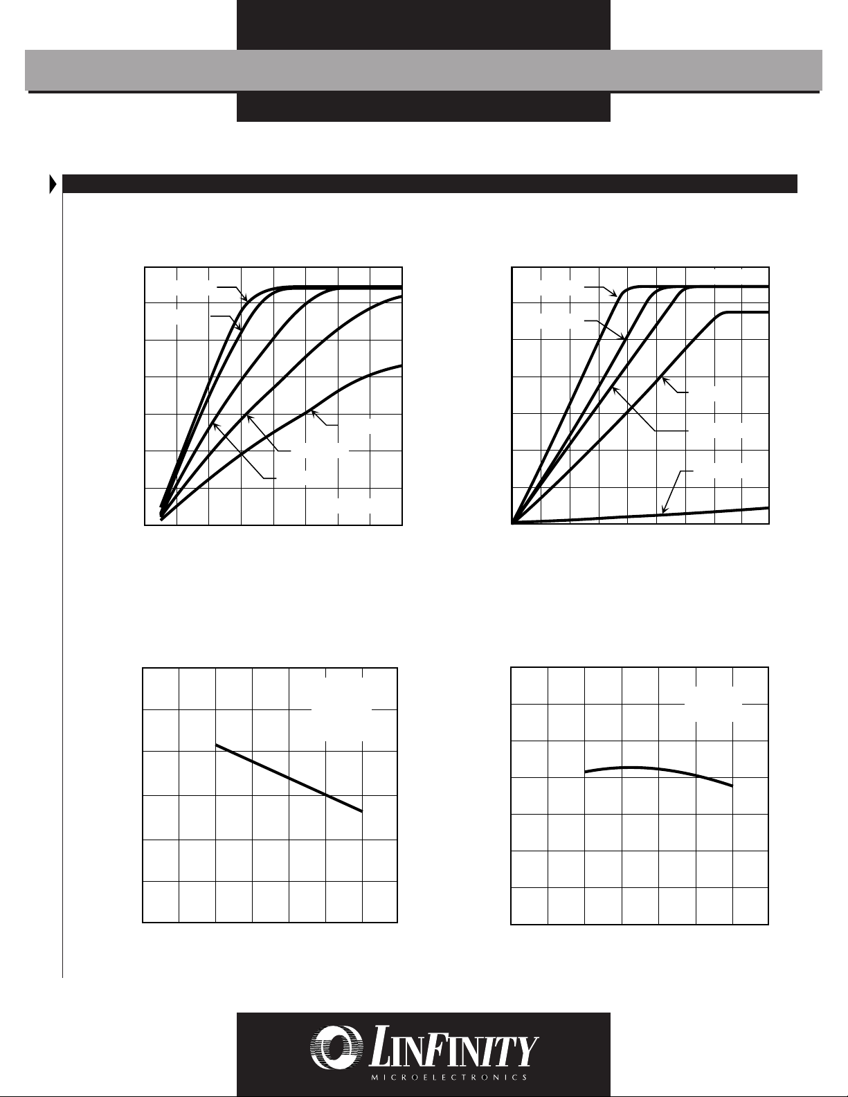
FIGURE 1. — E.A. OUTPUT VOLTAGE vs. C.S. THRESHOLD
1.4
VM1 = 3V
1.2
VM1 = 2.5V
1.0
0.8
0.6
C.S. Threshold - (V)
0.4
0.2
VM1 = 1.5V
VM1 = 2V
VM1 = 1V
TA = 25°C
0
2.6
2.4 2.8
3.233.43.6
3.8
E.A. Output Voltage - (V
FIGURE 3. — MULTIPLIER GAIN (V
vs. TEMPERATURE
=1V, V
M1
EA0
=3.5V)
FIGURE 2. —
1.4
1.2
1.0
0.8
0.6
0.4
C.S. Threshold Voltage - (V)
0.2
0
MULTIPLIER INPUT VOLTAGE vs. C.S. THRESHOLD
V
= 4V
EA0
V
= 3.5V
EA0
0.4
00.8
1.61.2 2 2.4
TA = 25°C
V
= 3V
EA0
V
= 3.25V
EA0
V
EA0
Multiplier Input Voltage - (V
FIGURE 4. — REFERENCE VOLTAGE (Including Offset)
vs. TEMPERATURE
= 2.5V
3.2
3.62.8
0.80
0.75
0.70
0.65
0.60
(K) Multiplier Gain - (1/V)
0.55
0.50
-50
Copyright © 1996
Rev. 1.3 12/96
-25 0
25
50 75 100 125
(TA) Ambient Temperature - (°C)
VCC = 12V
= 1nF
C
L
V
= 3.5V
EA0
V
= 1V
M1
7
Page 8
LX1562/1563
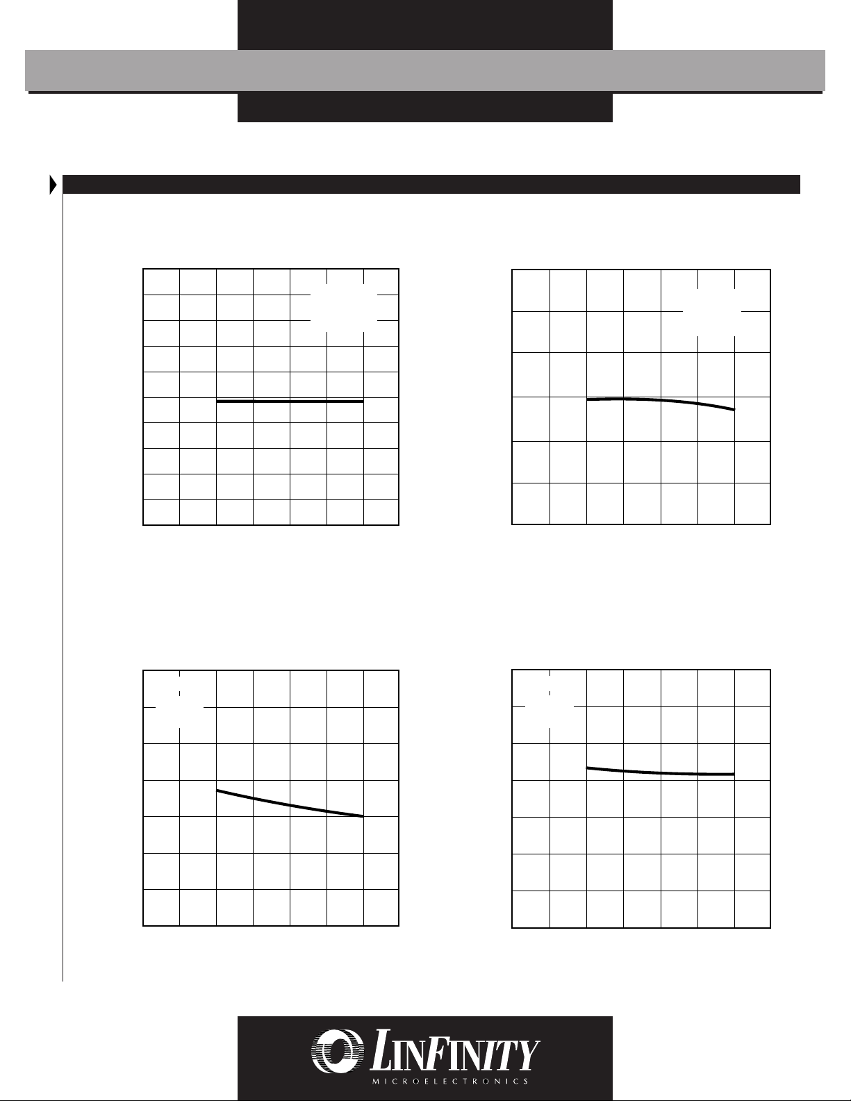
100.0
0.0
(TA) Ambient Temperature - (°C)
350.0
(I
ST
) Start-up Supply Current - (µA)
150.0
-50
-25 0
25
50 75 100 125
VIN < V
TH
CL = 1nF
50.0
200.0
250.0
300.0
LX1562
4.0
3.0
(TA) Ambient Temperature - (°C)
6.0
(I
SK
) E.A. Sink Current @2V - (mA)
4.5
-50
-25 0
25
50 75 100 125
VCC = 12V
C
L
= 1nF
V
EA0
= 2V
3.5
5.0
5.5
PRODUCT DATABOOK 1996/1997
S ECOND-GENERATION POWER FACTOR CONTROLLER
RODUCTION DATA SHEET
P
CHARACTERISTIC CURVES
FIGURE 5. — E.A. INPUT BIAS CURRENT vs. TEMPERATURE
0.5
0.4
0.3
0.2
0.1
0.0
-0.1
-0.2
) E.A. Input Bias Current - (µA)
-0.3
B
(I
-0.4
-0.5
-50
-25 0
25
VCC = 12V
C
= 1nF
L
E.A.- = 2.5V
50 75 100 125
FIGURE 6. —
E.A. SINK CURRENT @2V vs. TEMPERATURE
(TA) Ambient Temperature - (°C)
FIGURE 7. — START-UP SUPPLY CURRENT vs. TEMPERATURE FIGURE 8. — START-UP SUPPLY CURRENT vs. TEMPERATURE
350.0
LX1563
0.0
-50
VIN < V
CL = 1nF
-25 0
(TA) Ambient Temperature - (°C)
300.0
250.0
200.0
150.0
8
100.0
) Start-up Supply Current - (µA)
ST
50.0
(I
TH
25
50 75 100 125
Copyright © 1996
Rev. 1.3 12/96
Page 9

PRODUCT DATABOOK 1996/1997
9.60
9.40
(TA) Ambient Temperature - (°C)
(V
ST
) Start-up Threshold
-50 -25 0
25
50 75 100 125
9.50
LX1563
9.70
9.80
9.90
10.00
10.10
10.20
VCC = 0V to 16V
C
L
= 1nF
S ECOND-GENERATION POWER FACTOR CONTROLLER
P RODUCTION DATA SHEET
CHARACTERISTIC CURVES
LX1562/1563
FIGURE 9. — START-UP THRESHOLD vs. TEMPERATURE
14.0
FIGURE 10. —
START-UP THRESHOLD vs. TEMPERATURE
LX1562
13.5
13.0
12.5
12.0
) Start-up Threshold - (V)
ST
(V
11.5
11.0
-50
-25 0
25
VCC = 0V to 16V
= 1nF
C
L
50 75 100 125
(TA) Ambient Temperature - (°C)
FIGURE 11. — UV LOCKOUT HYSTERESIS vs. TEMPERATURE FIGURE 12. — UV LOCKOUT HYSTERESIS vs. TEMPERATURE
Copyright © 1996
Rev. 1.3 12/96
) UV Lockout Hysteresis - (V)
H
V
∆
(
6.0
5.5
5.0
4.5
4.0
3.5
3.0
-50
LX1562
-25 0
25
50 75 100 125
(TA) Ambient Temperature - (°C)
2.50
2.40
2.30
2.20
2.10
2.00
1.90
1.80
) UV Lockout Hysteresis - (V)
H
1.70
V
∆
(
1.60
1.50
LX1563
-50 -25 0
25
(TA) Ambient Temperature - (°C)
50 75 100 125
9
Page 10

LX1562/1563
250
150
(TA) Ambient Temperature - (°C)
500
(t
d
) C.S. Delay to Output - (ns)
300
-50
-25 0
25
50 75 100 125
VCC = 12V, CL = 1nF
V
M1
= 1V, V
EA0
= 3.7V
V
CS
= 0V to 1.2V
200
350
400
450
100
0
(TA) Ambient Temperature - (°C)
(H
D
) I
DET
Input Hysteresis - (mV)
-50 -25 0
25
50 75 100 125
50
150
200
250
300
350
400
PRODUCT DATABOOK 1996/1997
S ECOND-GENERATION POWER FACTOR CONTROLLER
RODUCTION DATA SHEET
P
CHARACTERISTIC CURVES
FIGURE 13. — I
1.90
1.85
1.80
1.75
1.70
Threshold High - (V)
1.65
DET
) I
1.60
HI
THRESHOLD HIGH vs. TEMPERATURE
DET
(V
1.55
1.50
-50 -25 0
25
50 75 100 125
(TA) Ambient Temperature - (°C)
FIGURE 15. — RUN-AWAY COMPARATOR THRESHOLD
vs. TEMPERATURE
FIGURE 14. —
I
INPUT HYSTERESIS vs. TEMPERATURE
DET
FIGURE 16. — C.S. DELAY TO OUTPUT vs. TEMPERATURE
2.8
2.6
2.4
2.2
10
2.0
1.8
1.6
Run-Away Comp. Threshold
1.4
1.2
-50 -25 0
25
50 75 100 125
(TA) Ambient Temperature - (°C)
Copyright © 1996
Rev. 1.3 12/96
Page 11

PRODUCT DATABOOK 1996/1997
80
40
(TA) Ambient Temperature - (°C)
(t
R
) Rise Time - (ns)
-50 -25 0
25
50 75 100 125
60
100
120
140
160
180
200
VCC = 12V
C
L
= 2200pF
200
0
(TA) Ambient Temperature - (°C)
600
(t
RST
) Restart Time - (µs)
300
-50
-25 0
25
50 75 100 125
VCC = 12V
C.S. = Pulse
100
400
500
S ECOND-GENERATION POWER FACTOR CONTROLLER
P RODUCTION DATA SHEET
CHARACTERISTIC CURVES
LX1562/1563
FIGURE 17. — C.S. BLANKING TIME vs. TEMPERATURE
1000
900
800
700
600
500
) C.S. Blanking Time - (ns)
BLK
(t
400
300
-50
-25 0
25
50 75 100 125
FIGURE 18. —
RESTART TIME vs. TEMPERATURE
(TA) Ambient Temperature - (°C)
FIGURE 19. — FALL TIME vs. TEMPERATURE FIGURE 20. — RISE TIME vs. TEMPERATURE
Copyright © 1996
Rev. 1.3 12/96
) Fall Time - (ns)
F
(t
90
80
70
60
50
40
30
20
-50
VCC = 12V, CL = 2200pF
-25 0
25
50 75 100 125
(TA) Ambient Temperature - (°C)
11
Page 12

LX1562/1563
PRODUCT DATABOOK 1996/1997
S ECOND-GENERATION POWER FACTOR CONTROLLER
RODUCTION DATA SHEET
P
CHARACTERISTIC CURVES
FIGURE 21. — SUPPLY CURRENT vs. SUPPLY VOLTAGE
14
LX1562
12
10
8
6
4
) Supply Current - (mA)
CC
(I
2
0
01020
30
TA = 25°C
= 0V
V
CS
V
= 0V
M1
V
= V
PIN2
PIN1
40 50 60
(VCC) Supply Voltage - (V)
FIGURE 22a. — MAXIMUM MULTIPLIER OUTPUT vs. TEMPERATURE
FIGURE 22. —
14
SUPPLY CURRENT vs. SUPPLY VOLTAGE
LX1563
12
10
8
6
4
) Supply Current - (mA)
CC
(I
2
0
01020
(VCC) Supply Voltage - (V)
30
TA = 25°C
= 0V
V
CS
V
= 0V
M1
V
= V
PIN2
PIN1
40 50 60
12
1.45
VCC = 12V, CL = 1nF
1.40
1.35
1.30
1.25
1.20
1.15
1.10
) Maximum Mult. Output Voltage - (V)
1.05
CLMP
(V
1.00
= 0V, VM1 = 2V, VCS = 0-2V
V
PIN1
-50
-25 0
25
50 75 100 125
(TA) Ambient Temperature - (°C)
Copyright © 1996
Rev. 1.3 12/96
Page 13

PRODUCT DATABOOK 1996/1997
Rectified
AC Line
GND
LX1562
GND
V
O
V
IN
IST < 300µA
I
1
> 300µA
C1
R1
R
S
D1
S ECOND-GENERATION POWER FACTOR CONTROLLER
P RODUCTION DATA SHEET
FUNCTIONAL DESCRIPTION
LX1562/1563
The operation of the IC is best described by referring to the
block-diagram. The output of the multiplier stage generates a
voltage proportional to the product of the rectified AC line and
the output of the error amplifier. This voltage serves as the
reference for the inductor peak current that is sensed by the
resistor in series with the external power MOSFET. When the
sense voltage exceeds this threshold, C.S. comparator trips and
resets the latch as well as turning the power MOSFET off.
The energy stored during switch on-time is now transferred
and stored in the output capacitor, causing the inductor current
Inductor Peak
Current Envelope
Average
AC Input Current
FIGURE 23 — INDUCTOR CURRENT
TONT
UNDERVOLTAGE LOCK OUT
The LX1562/63 undervoltage lock-out is designed to maintain
an ultra low quiescent current of less than 300µA, while guaranteeing the IC is fully functional before the output stage is
activated. Comparing this to the SG3561A device, a 40% reduction in start-up current is achieved, resulting in 40% less power
dissipation in the start-up resistor. This is especially important
in electronic ballast applications that are designed to operate in
harsh environments, with convection cooling as the only means
of heat dissipation.
Figure 24 shows an efficient supply voltage using the ultra
low start-up current of the LX1562 in conjunction with a bootstrap winding off of the power transformer. Circuit operation
is as follows:
The start-up capacitor (C1) is charged by current through
resistor (R1) minus the start-up current drawn by the IC. This
resistor is typically chosen to provide 2X the maximum start-up
current at low line to guarantee start-up under the worst case
condition. Once the capacitor voltage reaches the start-up
threshold, the IC turns on, starting the switching cycle. The
operation of the IC demands an increase in operating current
which results in discharging the capacitor. During the discharge
cycle, the flyback voltage of the auxiliary winding is rectified
and filtered via rectifier (D1) and charges the capacitor above
the minimum operating voltage of the device and takes over as
the supply voltage. The start-up capacitor and auxiliary winding must be selected such that it satisfies worst case IC conditions. Figure 25 shows start-up time and voltage of capacitor C1.
to ramp down. When current reaches zero level (inductor runs
out of energy) , boost diode (D1) stops conducting and the
residual inductor energy and the drain to source capacitance of
the power MOSFET create an LC tank circuit which causes drain
voltage to resonate at this frequency. The resonating voltage is
detected by the secondary winding (Idet winding) of the inductor. When this voltage swings negative “I detect” pin senses
it and activates the blanking circuit , sets the latch, and turns
power MOSFET on, repeating the cycle. This operation continues for the entire cycle of the AC rectified input resulting in an
inductor current as shown in Figure 23. The high frequency
I
L
content of this current is then filtered by the input capacitor
(C1) resulting in a sine wave input current in phase with the
AC line voltage.
Output voltage regulation is accomplished when the error
amplifier compares this voltage to an internal 2.5V reference
and generates an error voltage. This voltage then controls the
amplitude of the multiplier output adjusting the peak inductor
current proportional to the load and line variations, maintain-
OFF
ing a well regulated voltage.
IC DESCRIPTION
Table 1 shows the start-up voltage and hysteresis for LX1562
and LX1563. The LX1562 is used for stand alone pre-regulator
applications while LX1563 is ideal for applications where supply voltage is derived elsewhere and requires less than 14V
start-up.
FIGURE 24 — TYPICAL APPLICATION OF START-UP CIRCUITRY
T ABLE 1
Part # Start-Up Hysteresis
Voltage Voltage
LX1562 13.1V 5.2V
LX1563 9.8V 2.1V
Copyright © 1996
Rev. 1.3 12/96
13
Page 14

LX1562/1563
PRODUCT DATABOOK 1996/1997
S ECOND-GENERATION POWER FACTOR CONTROLLER
RODUCTION DATA SHEET
P
IC DESCRIPTION
VOLTAGE REFERENCE (continued)
V
C1
V
START
V
HYST
RT & CT TIME CONSTANT
FIGURE 25 — START-UP CAPACITOR VOLTAGE
C1
DISCHARGE
DISCHARGE
TIME
BOOTSTRAP
WINDING
VOLTAGE REFERENCE
The voltage reference is a low drift bandgap design which provides a stable +2.5V output with maximum of ±1.5% initial accuracy. This voltage is internally tied to the non-inverting input of the amplifier and is not available for external connection. The initial accuracy of the reference includes error amplifier input offset voltage. Figure 26 shows typical variation of
the reference voltage vs. temperature.
2.52
2.51
2.50
VCC = 12V
= 1nF
C
L
ERROR AMPLIFIER
The error amplifier is an internally compensated op-amp with
access to the inverting input and the output pin. The noninverting input is internally connected to the voltage reference
and is not available for external connection. The amplifier is
designed for an open loop gain of 80dB, along with a typical
bandwidth of 1.7MHz and 49 degrees of phase margin. The
boost output voltage of the power factor pre-regulator is divided down and monitored by the inverting input. Input bias
current (0.5µA max) can cause an output voltage error that is
equal to the product of the input bias current and the value of
the upper divider resistor. The amplifier's output is available
for external loop compensation. Typically, the loop bandwidth
is set below 10Hz in order to reject the low frequency ripple
associated with 2X the line frequency. For example, if the
t
error amplifier is configured as an integrator with 1.2Hz bandwidth, it will have 40dB ripple rejection at 120Hz frequency.
This means that if the output of the error amp is allowed to
have 100mV of ripple, the boost converter must be limited to
less than 10V of ripple on its output.
To prevent boost output run away condition that may occur
during removal of the output load, a separate comparator monitors the E.A. output voltage and compares it to an internal 1.8V
reference. When load is removed, E.A. output swings lower
than 1.8V, trips the comparator and turns output driver off till
the inverting input voltage drops below 2.5V. At this point, the
E.A. output swings positive, turns the output driver back on
and repeats the cycle until the load is returned to normal condition.
To reduce output overshoot during line and load transients,
the E.A. output is clamped to two diode drops above the reference voltage. This prohibits the amplifier from being saturated, allowing it to recover faster thus minimizing the boost
voltage overshoot.
2.49
2.48
2.47
) Reference Voltage - (V)
R
(V
2.46
2.45
-50
-25 0
25
50 75 100 125
(TA) Ambient Temperature - (°C)
FIGURE 26 — REFERENCE VOLTAGE (Including Offset) vs. TEMPERATURE
14
V
R10
O
R9
I
9
1
Bias
V
C4
REF
1.8V
From I
BW =
I9 >> I
2
Logic
DET
1
π
R9 C4
2
BIAS
2f
f = Line Freq.
FIGURE 27 — THE AMPLIFIER CONFIGURED AS AN INTEGRATOR
FOR LOOP COMPENSATION
OUTPUT
7
DRIVE
Copyright © 1996
Rev. 1.3 12/96
Page 15

PRODUCT DATABOOK 1996/1997
S ECOND-GENERATION POWER FACTOR CONTROLLER
P RODUCTION DATA SHEET
IC DESCRIPTION
MULTIPLIER
The LX1562/63 features a one quadrant multiplier stage having
two inputs. One (VM2) is internally driven by a DC voltage
which is the difference of E.A. output and V
is connected to an external resistor divider monitoring the rectified AC line. The output of the multiplier which is a function
of both inputs, controls inductor peak current during each cycle
of operation. This allows the inductor peak current to follow
the AC line thus forcing the average input current to be sinusoidal.
The multiplier is in the linear region if the V
to less than 2V and the E.A. output is kept below 3.5V under all
line and load conditions. The output is internally clamped to
1.24V typically to limit the MOSFET peak current during turn on
or under excessive load conditions. The equation below describes the relationship between multiplier output voltage and
the its inputs.
V
= K * V
M0
M1
*
(V
EA0
- V
REF
)
where: K = Multiplier gain (typ. 0.65)
V
= Voltage at pin3 (0 to 2V)
M1
V
= Error amp output voltage (2.5 to 3.5V)
EA0
= Multiplier output voltage
V
M0
E.A.
OUTPUT
2
V
EA
Σ
V
INV.
INPUT
AC
R1
R2
1
V
REF
2.5V
V
3
M1
FIGURE 28 — MULTIPLIER SECTION
CURRENT SENSE COMPARATOR
Current sense comparator is configured as a PNP input differential stage with one input internally tied to the multiplier output and the other available for current sensing. Current is converted to voltage using an external sense resistor in series with
the external power MOSFET. When sense voltage exceeds the
threshold set by the multiplier output, the current sense comparator terminates the gate drive to the MOSFET and resets the
PWM latch. The latch insures that the output remains in a low
state after the switch current falls back to zero. The LX1562/63
features a leading edge blanking circuit that eliminates the need
. The other (VM1),
REF
input is limited
M1
MULT.
OUTPUT
V
V
M2
M0
C.S.
INPUT
4
LX1562/1563
for an external RC filter otherwise required for proper operation of the circuit. This function is described in detail under
“current detect logic” section.
The current sense comparator voltage is limited by an internal 1.24V (typ.) voltage clamp of the multiplier output. Therefore maximum switch current is typically given by:
I
= 1.24V / R
PK (MAX)
Maximum switch peak current happens at full load and minimum line conditions.
TO
PIN 7
3
R
S
V
M0
5
FIGURE 29 — CURRENT SENSE SECTION
CURRENT DETECT LOGIC
The function of “current detect logic” is to sense the operating
state of the boost inductor and to enable the output driver
accordingly. To achieve this, the downward slope of the inductor current is indirectly detected by monitoring the voltage
across a separate winding and connecting it to the detector
input “I
level, the voltage across the winding reverses polarity and
changes the “I
state (See Figure 30). When comparator changes state, it sets
” pin. Once the inductor current reaches ground
DET
” input and the comparator output to the low
DET
the latch and turns on the output driver for a period of 1µs
(typ.) regardless of any changes in the latch output (Q) within
this period. This ensures that if the C.S. comparator changes
state due to any turn-on spike, the driver output remains on
and does not turn off prematurely.
However if the spike lasts longer than 1µs, the output driver
turns off and the MOSFET stops conducting. This type of digital current sense blanking which is not amplitude dependent
has higher noise immunity than the commonly used external
RC filtering, allowing for more flexibility in board layout.
Since inductor voltage swings both positive and negative,
internal voltage clamping is provided to protect the IC. The
S
Logic
Circuit
R
1µsec
Blank
7
Copyright © 1996
Rev. 1.3 12/96
15
Page 16

LX1562/1563
PRODUCT DATABOOK 1996/1997
S ECOND-GENERATION POWER FACTOR CONTROLLER
RODUCTION DATA SHEET
P
IC DESCRIPTION
CURRENT DETECT LOGIC (continued)
upper 7.8V clamp prevents input overvoltage breakdown dur-
switch off time, while during the on time the lower 0.7V
ing
clamp prevents substrate injection. An internal current limit
resistor protects the lower clamp transistor in case the “I
is accidently shorted to ground.
DET
” pin
START-UP TIMER
A start-up timer circuit eliminates the need for an external oscillator when used in stand alone applications. The timer, as
shown in Figure 30, provides a means to automatically start the
pre converter if the latch output Q comes up in a wrong (HI)
state. The timer capacitor ramps up and resets the latch to a
low state, turning the output driver on.
V
REF
I
DEF
300
Ω
5
L1
V
1.72V
TIMER
C.S.
C.S. Latch
OUTPUT DRIVER STAGE
The LX1562/63 output driver is designed for direct driving of
an external power MOSFET. It is a totem pole stage with
±500mA peak current capability. This typically results in a
130ns rise and fall times into a 1000pF capacitive load. Additionally the output is held low during the undervoltage condition to ensure that the MOSFET remains in the off state until
supply voltage reaches the start-up threshold.
Internal voltage clamping ensures that output driver is always lower than 13.8V (typ.) when supply voltage variation
exceeds more than rated V
nal MOSFET. This eliminates an external zener diode and extra
threshold (typ 20V) of the exter-
GS
power dissipation associated with it that otherwise is required
for reliable circuit operation.
HI
C.S.
V
M0
S
1µs
Delay
R
Q
Q
L1
OUT
7
C.S.
4
16
FIGURE 30 — START-UP TIMER & CURRENT DETECT LOGIC CIRCUITRY
Copyright © 1996
Rev. 1.3 12/96
Page 17

PRODUCT DATABOOK 1996/1997
A
S ECOND-GENERATION POWER FACTOR CONTROLLER
P RODUCTION DATA SHEET
APPLICATION INFORMATION
TYPICAL APPLICATION
The application circuit shown in Figure 31 uses the LX1562 as the
controller to implement a boost type power factor regulator. The
I.C. controls the regulator, such that the inductor current is always
operating in a discontinuous conduction mode with no current
gaps. This mode of operation has several advantages over the
fixed frequency discontinuous conduction mode: 1) The switching frequency adjusts itself to the AC line envelope, causing a
sinusoidal current draw, 2) Since there is no current gap between
the switching cycles, the inductor voltage does not oscillate,
causing less radiated noise, 3) The lower peak inductor current
causes less power dissipation in the power MOSFET.
LX1562/1563
A set of formulas have been derived specifically for this mode,
and are used throughout the design procedure. An example with
the following specifications for the boost converter is given as:
Input Voltage Range - 100 to 130V RMS
Output Power - 80W
Efficiency - 95% at full load
Power Factor - > 0.99 at full load
Total Harmonic Distortion - < 10% at full load
followed by a step by step design procedure which walks through
component selection.
AC-
C+
120V
AC
450µH
61T #22AWG
L1
100k
D1 D3
1N4004
1N4004
EMI FILTER
D2
C1
D4
1N4004
1N4004
Note: Thick trace on schematic shows high-frequency, high-current path in circuit.
FIGURE 31 — TYPICAL APPLICATION OF THE LX1562 IN AN 80W FLUORESCENT LAMP
½W
2.2M
R1
1%
1µF
250V
29k
R2
1%
Lead lengths must be minimized to avoid high-frequency noise problems.
7T
R3
D5
R10
4.7M
C4
.01µF
BALLAST WITH ACTIVE POWER FACTOR CONTROL
C2
22µF
R4
22k
1N4935
C3
0.1µF
8
V
IN
MULT
IN
3
LX1562
GND
6
I
DET
OUT
COMP
INV
C.S.
1N4148
47
7
R5
R9 620k
2
1
4
D6
5
Ω
C5
0.1µF
1/4W
3x
MR854
1M
Q1
1RF730
R6
1.3
Ω
D7
1%
11k
1%
V
BOOST
230V
Ω
R7
C6
100µF
400V
R8
FLOURESCENT LAMP BALLAST
OUTPUT VOLTAGE REQUIREMENT
Since the converter is a boost type topology, it requires the output
voltage to always be higher than the input voltage. It is
recommended to select this voltage at least 15% higher than the
maximum input voltage in order to: A) Avoid the inductor
saturation during line transience, and B) To keep the operating
frequency above the audible range at high line.
Figure 32 (next page) shows that when boost voltage is
selected near the maximum AC line, the increase in off-time could
reduce the operating frequency below the audible frequency and
cause inductor humming. In fact, Figure 32 (next page) shows
Copyright © 1996
Rev. 1.3 12/96
that for ±13% (100V to 130V) change in the line voltage the
optimum range of the operating frequency is when off-time duty
cycle (D') is between 0.57 and 0.75. This means that the boost
voltage needs to be 245V when selecting D' = 0.75 at maximum
AC line.
In this example, D' is chosen to be 0.8, to slightly reduce the
voltage rating of the back end DC to AC fluorescent lamp inverter.
This sets the boost voltage at:
130
√2
= = 230V
V
O
*
0.8
17
Page 18

LX1562/1563
PRODUCT DATABOOK 1996/1997
S ECOND-GENERATION POWER FACTOR CONTROLLER
RODUCTION DATA SHEET
P
APPLICATION INFORMATION
OUTPUT VOLTAGE REQUIREMENT (continued)
0.2
fn = (1 - D') D'²
0.15
0.1
2 V
D' =
0.05
f = f
) Normalized Operating Frequency
n
(f
0.3
0.4 0.5
AC
V
O
η
VO²
n
4 LP
O
0.6
0.7 0.8 0.9 1.0
(D') Off Time Duty Cycle
FIGURE 32 — NORMALIZED OPERATING FREQUENCY vs.
OFF-TIME DUTY CYCLE
INDUCTOR PEAK CURRENT
It can be shown by referring to Figure 33 that the inductor peak
current is always twice the average input current.
Inductor Peak
Current Envelope
Average
AC Input Current
FIGURE 33 — INDUCTOR CURRENT
I
= AVE [ IL (t) ]
IN(t)
Σ
(IL) (T)
1
I
IN
I
INpeak
I
LP
==
T
= IP =
2
I
LP
2
= Inductor peak current at peak input voltage.
I
L
2
I
L
TONT
OFF
Maximum peak input current can be calculated using:
2P
O
=
I
P
ηV
P
where: η≡Converter efficiency
V
≡ Peak AC input voltage
P
assuming: η = 95%, P
2 x 80
= = 1.2A
I
P
(.95)(141)
I
= 2 * 1.2 = 2.4A
LP/min AC
= 80W, V
O
= 100√2 = 141
Pmin
INDUCTOR DESIGN
The inductor value is calculated assuming a 50KHz operating
frequency at the nominal AC voltage using the following equation:
VO - V
P
O
O
230 - 120√2
230
2
P
4 * 80
V
≡ Output DC voltage
O
≡ Peak AC input voltage
V
P
T ≡ Switching period
≡ Output Power
P
O
(120√2)
*
2
η T V
= where: η≡Efficiency
L
1
L1 = = 448µH
V
4 P
.95 ( ) 20 * 10-6
choose T = 20µsec (50kHz)
Figure 32 shows that at nominal AC line (D' = 0.74) the normalized
frequency is 0.142 and dropping to 0.13 at maximum line
condition. This translates to a 10% drop in operating frequency
which is still well above the audible range.
Once the inductance is known, we can either use the area
product method (AP) or the K
for selecting proper core size. In this example, we apply the K
(based on copper losses method),
g
approach using the following steps:
Step 1: Calculate K
=( )
K
g
where: L
g
Ω
P
CU
1
Ω≡1.724
using
2
L1I
LP
2
B
≡ Required inductance
-8
10
m
*
B ≡ Maximum flux density
≡ Maximum peak inductor current
I
LP
P
≡ Maximum copper dissipation
CU
Assume: P
1.724 * 10
= = 3.21 * 10
K
g
1.6
= 1.6W (2% of total output)
CU
-8
450 * 10
-6
0.15
* (2.4)
2
2
-12 m5
g
18
Copyright © 1996
Rev. 1.3 12/96
Page 19

PRODUCT DATABOOK 1996/1997
S ECOND-GENERATION POWER FACTOR CONTROLLER
P RODUCTION DATA SHEET
APPLICATION INFORMATION
LX1562/1563
INDUCTOR DESIGN (continued)
Step 2: Choose a core with higher Kg than the one calculated in
Step 1.
Kg/core = k
AW A
l
2
E
W
where: k ≡ Winding coefficient (typ. k=0.4)
A
≡ Bobbin window area
W
≡ Effective core area
A
E
l
≡ Mean length per turn
W
K
factor for TDK PQ2625:
g
= 47.7mm
A
W
AE= 118mm
2
2
lW= 56.2mm
56.2
2
-12 m5
(47.7) (118)
= 0.4 (mm)5 = 4.7 * 10
K
g
Step 3: Determine number of turns.
L I
N =
N = = 61 turns
A
LP
B A
E
450 * 10-6 * 2.4
0.15 * 118 * 10
A
W
= k = 0.4 = 0.31mm
WIRE
N
-6
47.7
61
= 480mil
2
2
choose #22 AWG with r = 0.0165Ω/feet resistance.
R
= N * lw * r
W
R
= 0.185Ω
W
Step 4: Calculate air gap.
µO N2 A
4π
*
L
10
E
-7
(61)
*
450 * 10
2
118*10
*
-6
-6
=
l
g
l
= = 0.122cm = 48 mil
q
CURRENT SENSE RESISTOR
Current sense resistor, R6 is selected using the minimum multiplier output clamp voltage and the maximum inductor peak
current such that:
V
CLAMP(MIN)
R6 = = = 0.45Ω
I
L (MAX)
1.1
2.4
Power dissipation is approximated by:
1
≈ I
P
R
6
1
P
≈ (2.4)
R
6
2
(1 - D'
2 (MAX)
2
(1 - 0.61) = 0.374
), where D'
MIN
MIN
= 1 -
√2 V
V
AC(MIN)
BOOST
Select THREE 1.3Ω , ¼W carbon comp resistors in parallel.
MULTIPLIER COMPONENT SELECTION
Calculate R1 & R2 resistor values such that under low line AC input
the multiplier output is lower than the minimum clamp voltage.
R2
R1 + R2
√2 V
*
AC (MIN)
* K * (V
EA0 (MAX)
- V
REF
) < V
CLAMP (MIN)
where: K ≡ Mult. Gain
V
≡ Maximum error amp output where
EA)(MAX)
multiplier is still in linear range.
This voltage is ≈ 3.5V.
For K = 0.65 & V
R1
> 83
R2
CLAMP (MIN)
= 1.1V, the ratio of R1/R2 is:
Assuming R1 is selected to be:
* R1 = 2.2M (1%)
2.2M
R2 = = 26.4k (1%) select R
83
= 26.7k (1%)
2
* For high input applications such as 277V, R1 must be divided
into two resistors in series to meet the maximum rated voltage of
the resistors.
To improve THD further (typ. 2-3%), a high value resistor can
be connected from the supply voltage to this pin to allow an
increase in the switch on-time at the zero crossing by adding an
effective offset at the multiplier output.
ERROR AMPLIFIER COMPONENT SELECTION
Boost voltage is programmed with R7 & R8 resistor dividers using
the following equation:
R7
R8
V
BOOST
= -1,
V
REF
assuming that the product of R7 and the E.A. input bias current
does not cause significant error in the output voltage setting.
ΩΩ
Assuming R7 = 1M
two resistors may be added in series to meet the voltage
requirement of the resistor.)
∆V
(106) (0.5 * 10-6) = 0.5V, which is < 0.25% of the
ERROR
(for output voltage of higher than 250V,
Ω
ΩΩ
output voltage.
Calculating R8:
V
BOOST
V
REF
R7
- 1
R8 = = 11k (1%)
Worst case output tolerance is the total of ±3.75% which is the sum
of ±1.5% (Ref), ±2% (resistor dividers), and ±0.25% (E.A. input
bias current).
Copyright © 1996
Rev. 1.3 12/96
19
Page 20

LX1562/1563
PRODUCT DATABOOK 1996/1997
S ECOND-GENERATION POWER FACTOR CONTROLLER
RODUCTION DATA SHEET
P
APPLICATION INFORMATION
ERROR AMPLIFIER COMPONENT SELECTION (continued)
Capacitor C5 is primarily selected to reject the output ripple
associated with twice the line frequency. For a 40dB ripple
rejection:
C5 ≥ where f
C5 ≥ = 0.062µF, Select C5 = 0.1µF
100
2π f
R7
l
2π
120*2.2*10
*
100
= 2x line frequency
l
6
Resistor R9 can be used to improve load transient response at the
cost of loosing 1 or 2% of load regulation. The value of this resistor
should be much greater than R8:
R9 = 620k
One way of achieving desired load transient response without
resorting to a complex mathematical model of the converter, is to
dynamically switch the output load and empirically find the
compensation network. The value of resistor R9 is selected using
the method shown in Figure 34.
V
BOOST
Min.
R
L
10Hz
50% D.C.
FIGURE 34 — LOAD TRANSIENT RESPONSE CIRCUIT
I
COMPONENT SELECTION
DETECT
Load
Figure 35 shows voltage envelope generated by flyback voltage
across I
Select turns ratio n such that,
n =
n = = 0.11
I
selected to be 7T.
winding:
DET
5V
- √2 V
V
BOOST
5V
230 - √2
winding turns are
DET
*
130
AC (MAX)
(V
- VAC)
n
BOOST
V
n
AC
FIGURE 35 — FLYBACK VOLTAGE
ACROSS I
WINDING
DET
and R4 resistor:
n * V
BOOST
< R4 < 500k
-3
3 * 10
0.11 * 230
3 * 10
< R4 < 500k, or 8.4k < R4 < 500k
-3
Select R4 = 22k
SUPPLY VOLTAGE
Resistor R3 must be selected such that it ensures converter startup at low line and is rated for high line power dissipation.
√2 V
R3 < where: I
R3 < = 466kΩ
R3 > 4 V
AC (MIN)
I
ST (MAX)
√2
100
*
0.3 * 10
-3
(to keep power dissipation below 0.5W)
AC (MAX)
≡ Maximum start-up
ST
V
ST
T
ST(MAX)
current
≡ Start-up voltage
≡ Maximum start-up
time at AC power-on
R3 > 68k , select R3 = 120k.
Start-up time of converter is given by:
V
T
ST (MAX)
≈ C2
√2 V
AC (MIN)
R3
ST
- I
ST
for our application this will be 25ms/µF.
The start-up capacitor is selected such that capacitor discharge
time is always longer than the time it takes for the bootstrap
voltage to reach above the minimum start-up threshold of the IC.
I
* ∆t
C3 < where: I
OP
∆V
MIN
≡ Maximum dynamic
OP
supply current of the IC
∆t ≡ Rise time of the
bootstrap voltage
≡ Minimum hysteresis
∆V
MIN
10 * 10-3 * 10 * 10
C3 < = 29µF
4
-3
(4V for 1562,
voltage
1.7V for 1563)
Select C3 = 33µF.
Start-up time is approximately 0.8 seconds.
The auxiliary winding turns are selected such that it provides 15V
of operating voltage.
V
N
≈ N
S
S
* = 61 * = 4T
P
V
O
However, in this example I
which eliminates the need for a third winding. This is possible
V
S
V
O
winding is used to power the IC
DETECT
since the internal clamping of the output drive limits the gate
drive voltage to 14V (typ.) if the supply voltage exceeds this limit.
20
Copyright © 1996
Rev. 1.3 12/96
Page 21

PRODUCT DATABOOK 1996/1997
S ECOND-GENERATION POWER FACTOR CONTROLLER
P RODUCTION DATA SHEET
APPLICATION INFORMATION
POWER MOSFET SELECTION
The voltage rating of MOSFET and rectifier must be higher than
the maximum value of the output voltage.
≥ 1.2 V
V
DS
O MAX
The RMS current can be approximated by multiplying the RMS
current at the peak of the line by 0.7.
I
= 0.7 I
RMS
D = 0.39 at V
I
= (0.7)(2.4)(√.39/3) = 0.61A
I
RMS
R
P
√D/3 D ≡ On-time duty cycle
LP
= 2.4A
LP
≤
DS
≡ allowable power I
DC
AC
P
DC
2
I
RMS
dissipation.
1
≤ = 1.6Ω
R
DS
0.61
IRF730 with R
requirements.
DS
= 1
INPUT RECTIFIER AND CAPACITOR SELECTION
The current through each diode is a half-wave rectified sine wave.
The maximum current happens at minimum line with a peak
value of 1.2A.
I
I
PEAK
= = = 0.38A
AVE
π
choose 1N4004 with 1A rating.
= (I
P
DISS
= TA + P
T
J
T
= 80 + (.344)(65) = 102°C
J
) (VF) = 0.38 x 0.9 = 0.344W
AVE
x θ
D
JA
= 100V
ΩΩ
Ω and V
ΩΩ
1.2
π
V
≥ 282V
DS
RMS
= 400V meets the above
DS
assuming θ
lead length.
= 65°C/W for 1/8"
JA
I
LP
D
/triangle = I
√D/3
LP
LX1562/1563
Assuming ϕ is the percentage of allowable input current ripple,
C1 can be calculated using the following equations:
2 P
R
EFF
C1 ≥ f
if ϕ = 3%
R
EFF
C1 ≥ = 0.9µF
choose 1µF, 250V capacitor.
OUTPUT CAPACITOR SELECTION
There are mainly two criteria for selecting the output capacitor:
A large enough capacitance to maintain a low ripple voltage, and
a low ESR value in order to prevent high power dissipation due
to RMS currents.
The output capacitance can be approximated from the following
equation:
C6 ≥ where: I
I
DC
assuming 5% peak to peak ripple,
C6 ≥ = 81µF
choose C6 = 100µF.
O
=
2
η I
P
1
ϕ 2π R
EFF fSW
2 x 80
= = 117Ω
(.95)(1.2)
2
1
(.03)(2π)(117)(50000)
I
DC
2π f
∆V
LINE
80
= = 0.348A
230
0.348
2π (60) (11.5)
≡ Switching frequency
SW
of inductor current
at peak input voltage.
≡ DC output current
DC
DV ≡ Output ripple
Copyright © 1996
Rev. 1.3 12/96
21
Page 22

LX1562/1563
PRODUCT DATABOOK 1996/1997
S ECOND-GENERATION POWER FACTOR CONTROLLER
RODUCTION DATA SHEET
P
TYPICAL APPLICATIONS
120V
450µH
L1
61T
#22AWG
D7
V
BOOST
R3
D3
D1
AC+
AC-
120V
AC
R1
C1
R2
D2 D4
Note: Thick trace on schematic shows high-frequency, high-current path in circuit. Lead lengths
must be minimized to avoid high-frequency noise problems.
FIGURE 36 — TYPICAL APPLICATION OF THE LX1562 IN AN 80W
FLUORESCENT LAMP BALLAST WITH ACTIVE POWER FACTOR CONTROL.
Electrical
Specification
Ref. Component Manuf.
120VAC Input — 230VDC / 80W Output
7T
D5
C4
#26AWG
R4
C2
R10
3
C3
IC LX1562 Linfinity
L1 PQ2625/H7C1 Core TDK
Q1 IRF730, 400V, 1Ω rds I.R.
D1-D4 IN4004 1A, 400V Motorola
D5 1N4935 1A Motorola
D6 1N4148
(improves Q1 power dissipation)
Motorola
D7 MR854, 3A, 400V Motorola
R1 2.2MΩ , ±1%
R2 26.7kΩ, ±1%
R3 100kΩ, ½W
R4 22kΩ
R5 47Ω
R6 1.5Ω, Carbon type (3X)
R7 1MΩ, 1%
R8 11kΩ, 1%
R9 620kΩ
(improves load transient response)
R10 4.7MΩ
A complete evaluation board is available from Linfinity Microelectronics Inc.
MULT
IN
8
V
IN
5
I
DET
D6
R7
R5
OUT
COMP
LX1562
INV
GND
C.S.
6
7
R9
2
C5
1
4
Q1
C6
R8
R6
Ref. Component Manuf.
C1 QXF2E105KRPT
1µF/250V - Plastic Film (high freq.) Nichicon
C2 22µF/35V - Electrolytic
C3 0.1µF/50V - Ceramic
C4 0.01µF/50V - Ceramic
C5 0.1µF/50V - Ceramic
C6 LGQ2G101MHS A/Z* Nichicon
100µF/400V - Electrolytic
* A = 25mm diam.
Z = 22mm diam.
FLOURESCENT LAMP BALLAST
22
Copyright © 1996
Rev. 1.3 12/96
Page 23

A
C+
AC-
220V
AC
D1
D3
D2 D4
PRODUCT DATABOOK 1996/1997
S ECOND-GENERATION POWER FACTOR CONTROLLER
P RODUCTION DATA SHEET
TYPICAL APPLICATIONS
220V
L1
1.2mH
C1
R3
80T
7T
4T
R1
R2
C4
R10
C2
#24AWG
#26AWG
#26AWG
D5
3
C3
MULT
IN
V
R4
8
IN
GND
6
5
I
DET
OUT
COMP
LX1562
INV
C.S.
D6
7
2
1
4
R5
R9
C5
Q1
R6
LX1562/1563
D7
R7
R8
V
BOOST
C6
FLOURESCENT LAMP BALLAST
Note: Thick trace on schematic shows high-frequency, high-current path in circuit. Lead lengths
must be minimized to avoid high-frequency noise problems.
FIGURE 37 — TYPICAL APPLICATION OF THE LX1562 IN AN 80W
FLUORESCENT LAMP BALLAST WITH ACTIVE POWER FACTOR CONTROL.
Electrical
Specification
Ref. Component Manuf.
IC LX1562 Linfinity
L1 PQ2625/H7C1 Core TDK
Q1 IRF830, 500V, 1.5Ω rds I.R.
D1-D4 IN4007 1A, 1000V Motorola
D5 1N4935 1A Motorola
D6 1N4148
D7 MR856, 3A, 600V Motorola
R1 2.2MΩ , ±1%
R2 12kΩ, ±1%
R3 220kΩ, ½W
R4 22kΩ
220VAC Input — 400VDC / 80W Output
Ref. Component Manuf.
C1 QXF2J224KRPT
0.22µF/630V - Plastic Film Nichicon
C2 22µF/35V - Electrolytic
C3 0.1µF/50V - Ceramic
C4 0.01µF/50V - Ceramic
(improves Q1 power dissipation)
Motorola
C5 0.1µF/50V - Ceramic
C6* LGQ2W680MHS A/Z* Nichicon
68µF/450V - Electrolytic
* A = 25mm diam.
Z = 22mm diam.
R5 47Ω
R6 1.8Ω, Carbon type (2X)
R7 1MΩ, 1%
R8 6.19kΩ, 1%
R9 620kΩ
(improves load transient response)
R10 2.7MΩ
A complete evaluation board is available from Linfinity Microelectronics Inc.
Copyright © 1996
Rev. 1.3 12/96
23
Page 24

LX1562/1563
V
IN
I
DET
OUT
COMP
INV
C.S.
GND
MULT
LX1562
Q1
V
BOOST
FLOURESCENT LAMP BALLAST
IN
5
8
7
2
1
4
6
3
277V
AC
R4
R3
R1
C1
R2
C4
D5
C2
R5
C5
R7
A
C6
A
D7
R8
R9
R6
D6
AC+
AC-
D1
L1
2.2mH
15T
D3
D2 D4
C3
#24AWG
#26AWG
80T
#26AWG
3T
R10
R7
B
C6
B
PRODUCT DATABOOK 1996/1997
S ECOND-GENERATION POWER FACTOR CONTROLLER
RODUCTION DATA SHEET
P
TYPICAL APPLICATIONS
277V
24
Note: Thick trace on schematic shows high-frequency, high-current path in circuit. Lead lengths
must be minimized to avoid high-frequency noise problems.
FIGURE 38 — TYPICAL APPLICATION OF THE LX1562 IN AN 80W
FLUORESCENT LAMP BALLAST WITH ACTIVE POWER FACTOR CONTROL.
Electrical
Specification
Ref. Component Manuf.
IC LX1562 Linfinity
L1 PQ2625/H7C1 Core TDK
Q1 IRF830, 500V, 1.5Ω rds I.R.
D1-D4 IN4007 1A, 1000V Motorola
D5 1N4935 1A Motorola
D6 1N4148
277VAC Input — 480VDC / 80W Output
(improves Q1 power dissipation)
Motorola
D7 MR856, 3A, 600V Motorola
R1 2.2MΩ , ±1%
R2 10kΩ, ±1%
R3 390kΩ, ½W
R4 22kΩ
R5 47Ω
R6 2.2Ω, Carbon type (2X)
R7 499kΩ, 1% (2X)
R8 5.23kΩ, 1%
R9 620kΩ
R10 2.2MΩ
(improves load transient response)
A complete evaluation board is available from Linfinity Microelectronics Inc.
Ref. Component Manuf.
C1 QXF2J224KRPT
C2 22µF/35V - Electrolytic
C3 0.1µF/50V - Ceramic
C4 0.01µF/50V - Ceramic
C5 0.22µF/50V - Ceramic
C6 UVZ2F470MEH (2X) Nichicon
0.22µF/630V - Plastic Film Nichicon
47µF/315V - Electrolytic
Copyright © 1996
Rev. 1.3 12/96
Page 25

PRODUCT DATABOOK 1996/1997
A
S ECOND-GENERATION POWER FACTOR CONTROLLER
P RODUCTION DATA SHEET
TYPICAL APPLICATIONS
LX1562/1563
C+
90-265V
AC
AC-
#24AWG
#26AWG
#26AWG
D5
90V - 265V
R4
8
V
IN
5
I
DET
D6
D1
D3
R3
R1
62T
7T
L1
450µH
3T
C2
R5
C1
OUT
7
R9
MULT
IN
3
R2
D2 D4
Note: Thick trace on schematic shows high-frequency, high-current path in circuit. Lead lengths
must be minimized to avoid high-frequency noise problems.
C4
C3
LX1562
GND
6
COMP
INV
C.S.
2
C5
1
4
Q1
R6
D7
R7
R8
V
BOOST
C6
FLOURESCENT LAMP BALLAST
FIGURE 39 — TYPICAL APPLICATION OF THE LX1562 IN AN 80W
FLUORESCENT LAMP BALLAST WITH ACTIVE POWER FACTOR CONTROL.
Electrical
Specification
Ref. Component Manuf.
IC LX1562 Linfinity
L1 PQ2625/H7C1 Core TDK
Q1 IRF840, 500V, 1Ω rds I.R.
D1-D4 IN4007 1A, 1000V Motorola
D5 1N4935 1A Motorola
D6 1N4148
D7 MR856, 3A, 600V Motorola
R1 2.2MΩ , ±1%
R2 16.3kΩ, ±1%
R3 130kΩ, ½W
R4 22kΩ
90-265VAC Input — 400VDC / 80W Output
Ref. Component Manuf.
C1 QXF2J224KRPT
0.47µF/630V - Plastic Film Nichicon
C2 22µF/35V - Electrolytic
C3 0.1µF/50V - Ceramic
C4 0.01µF/50V - Ceramic
(improves Q1 power dissipation)
Motorola
C5 0.33µF/50V - Ceramic
C6* LGQ2W680MHS A/Z* Nichicon
68µF/450V - Electrolytic
* A = 25mm diam.
Z = 22mm diam.
R5 47Ω
R6 1Ω, Carbon type (4X)
R7 1MΩ, 1%
R8 6.19kΩ, 1%
R9 620kΩ
(improves load transient response)
A complete evaluation board is available from Linfinity Microelectronics Inc.
Copyright © 1996
Rev. 1.3 12/96
25
 Loading...