

Page 1

ICN Mini Link User’s Guide
1731N Model A – Mini Link Board for PC AT (Version 1)
1732N Model A – ICN Interface Board (Version 1)
Page 2

MicroMod Automation, Inc.
The Company
MicroMod Automation is dedicated to improving customer efficiency by providing the most cost-effective, application-specific process solutions
available. We are a highly responsive, application-focused company with years of expertise in control systems design and implementation.
We are committed to teamwork, high quality manufacturing, advanced technology and unrivaled service and support.
The quality, accuracy and performance of the Company's products result from over 100 years experience, combined with a continuous
program of innovative design and development to incorporate the latest technology.
Use of Instructions
Ì Warning. An instruction that draws attention to the risk of
injury or death.
Note. Clarification of an instruction or additional
information.
q Caution. An instruction that draws attention to the risk of
the product, process or surroundings.
Although Warning hazards are related to personal injury, and Caution hazards are associated with equipment or property damage, it
must be understood that operation of damaged equipment could, under certain operational conditions, result in degraded process
system performance leading to personal injury or death. Therefore, comply fully with all Warning and Caution notices.
Information in this manual is intended only to assist our customers in the efficient operation of our equipment. Use of this manual for
any other purpose is specifically prohibited and its contents are not to be reproduced in full or part without prior approval of MicroMod
Automation, Inc.
Licensing, Trademarks and Copyrights
MOD 30 and MOD 30ML are trademarks of MicroMod Automation, Inc.
MODBUS is a trademark of Modicon Inc.
Health and Safety
To ensure that our products are safe and without risk to health, the following points must be noted:
The relevant sections of these instructions must be read carefully before proceeding.
1. Warning Labels on containers and packages must be observed.
2. Installation, operation, maintenance and servicing must only be carried out by suitably trained personnel and in accordance with the information
given or injury or death could result.
3. Normal safety procedures must be taken to avoid the possibility of an accident occurring when operating in conditions of high
4. pressure and/or temperature.
5. Chemicals must be stored away from heat, protected from temperature extremes and powders kept dry. Normal safe handling procedures must be
used.
6. When disposing of chemicals, ensure that no two chemicals are mixed.
Safety advice concerning the use of the equipment described in this manual may be obtained from the Company address on the back
cover, together with servicing and spares information.
i Information. Further reference for more detailed
information or technical details.
All software, including design, appearance, algorithms and source
codes, is copyrighted by MicroMod Automation, inc. and is owned by
MicroMod Automation or its suppliers.
Page 3

IB-23C003
CONTENTS
––––––––––––––––––––––––––––––––––––––––––––––––––––––––––––––––––––––––––––––––––––––––––––
CONTENTS
Page
SECTION 1 - INTRODUCTION
1.1 DESCRIPTION . . . . . . . . . . . . . . . . . . . . . . . . . . . . . . . . . . . . . . . . . . . . . . 1-1
1.2 EXPLANATION OF SERIAL AND CATALOG NUMBER . . . . . . . . . . . . . . . . . . 1-2
1.3 PRODUCT DESCRIPTIONS . . . . . . . . . . . . . . . . . . . . . . . . . . . . . . . . . . . . . 1-3
1.3.1 1731N Mini Link Board for AT Style PC . . . . . . . . . . . . . . . . . . . . . . . . . . . 1-3
1.3.2 1732N ICN Interface Board . . . . . . . . . . . . . . . . . . . . . . . . . . . . . . . . . . . . 1-4
1.4 TECHNICAL SUMMARY . . . . . . . . . . . . . . . . . . . . . . . . . . . . . . . . . . . . . . . 1-5
1.5 RELATED DOCUMENTATION . . . . . . . . . . . . . . . . . . . . . . . . . . . . . . . . . . . 1-7
SECTION 2 - INSTALLATION
2.1 PREPARING THE PERSONAL COMPUTER . . . . . . . . . . . . . . . . . . . . . . . . . 2-1
2.2 DETERMINING MINI LINK BASE ADDRESS/INTERRUPT LEVEL . . . . . . . . . . 2-2
2.3 INSTALLING THE MINI LINK BOARD . . . . . . . . . . . . . . . . . . . . . . . . . . . . . . 2-2
2.4 SWITCH AND JUMPER SETTINGS . . . . . . . . . . . . . . . . . . . . . . . . . . . . . . . 2-3
2.4.1 Serial Ports . . . . . . . . . . . . . . . . . . . . . . . . . . . . . . . . . . . . . . . . . . . . . . . 2-3
2.4.2 ICN . . . . . . . . . . . . . . . . . . . . . . . . . . . . . . . . . . . . . . . . . . . . . . . . . . . . . 2-6
SECTION 3 - PROGRAMMING MINI LINK INTERRUPTS
3.1 GENERAL . . . . . . . . . . . . . . . . . . . . . . . . . . . . . . . . . . . . . . . . . . . . . . . . . . . . . 3-1
3.2 COMMUNICATIONS POLLING (NO INTERRUPTS) . . . . . . . . . . . . . . . . . . . . . . . . 3-1
3.3 COMMUNICATIONS USING INTERRUPT SERVICE ROUTINES . . . . . . . . . . . . . . . 3-1
SECTION 4 - TROUBLESHOOTING THE MINI LINK
4.1 NO RESPONSE FROM LINK . . . . . . . . . . . . . . . . . . . . . . . . . . . . . . . . . . . . . . . . 4-1
4.2 PARITY, FRAMING OR OVERRUN ERROR . . . . . . . . . . . . . . . . . . . . . . . . . . . . . 4-1
4.3 FROZEN DISPLAY/NO RESPONSE FROM PC KEYBOARD . . . . . . . . . . . . . . . . . . 4-2
4.3 NO RESPONSE FROM THE FIELD INSTRUMENTS . . . . . . . . . . . . . . . . . . . . . . . 4-2
APPENDIX A - ALPHANUMERIC LISTING OF JUMPERS AND SWITCHES
APPENDIX B - CONNECTOR DESCRIPTIONS
ILLUSTRATIONS
Figure Page
1-1 Mini Link Module . . . . . . . . . . . . . . . . . . . . . . . . . . . . . . . . . . . . . . . . . . . . . . 1-1
A-1 Switch and Jumper Locations for 1731N Mini Link . . . . . . . . . . . . . . . . . . . . . . A-1
A-2 Switch and Jumper Locations for 1732N ICN Interface Board . . . . . . . . . . . . . . . A-2
i
Page 4

IB-23C003
CONTENTS
–––––––––––––––––––––––––––––––––––––––––––––––––––––––––––––––––––––––––––––––––––––––––––
TABLES
Table Page
2-1 Personal Computer Device Inventory . . . . . . . . . . . . . . . . . . . . . . . . . . . . . . . . 2-1
2-2 DIP Switch SW2, PC/AT Serial Port Base Address . . . . . . . . . . . . . . . . . . . . . . 2-3
2-3 Mini Link Hardware Interrupts . . . . . . . . . . . . . . . . . . . . . . . . . . . . . . . . . . . . . 2-4
2-4 Mini Link Interrupt Polarity . . . . . . . . . . . . . . . . . . . . . . . . . . . . . . . . . . . . . . . . 2-4
2-5 Mini Link PC/AT Serial Port Baud Rates . . . . . . . . . . . . . . . . . . . . . . . . . . . . . . 2-4
2-6 Mini Link External Serial Port Baud Rates . . . . . . . . . . . . . . . . . . . . . . . . . . . . . 2-5
3-1 Interrupt Service Vector Locations . . . . . . . . . . . . . . . . . . . . . . . . . . . . . . . . . . 3-2
A-1 Alphanumeric Listing of Jumpers and Switches for 1731N Mini Link . . . . . . . . . . A-1
A-2 Alphanumeric Listing of Jumpers and Switches for 1732N ICN Interface Board . . A-2
B-1 IBM PC/AT Mini Link Board Connector Pinout . . . . . . . . . . . . . . . . . . . . . . . . . B-1
B-2 Mini Link RS-232 Connector Pinout . . . . . . . . . . . . . . . . . . . . . . . . . . . . . . . . . B-2
B-3 Mini Link ICN0 and ICN1 Connector Pinout . . . . . . . . . . . . . . . . . . . . . . . . . . . B-2
ii
Page 5

1.1 DESCRIPTION
The 1731N Mini Link with 1732N ICN Interface Board, Figure 1-1, provides a general
purpose serial interface to MOD 30 and MODCELL instruments via the Instrument
Communications Network (ICN). The 1731N Mini Link supports one ICN and the 1732N
ICN Interface Board supports a second ICN. The Mini Link provides intelligent buffers that
enable the operation of higher level devices (such as personal or other computers) by:
• Assembling display and tuning information for a number of instruments and storing the
data in block format. This relieves the host from executing individual requests and
improves the efficiency of the communications.
• Permitting the host device to download and upload instrument configuration
information. This enables instrument configuration to be performed at a central
location using a personal computer that can easily display, manipulate and document
data.
IB-23C003
INTRODUCTION
SECTION 1
INTRODUCTION
• Permitting limited peer-to-peer communications between ICNs.
• Providing diagnostic checks for message validity resulting in secure general purpose
serial interfaces to the ICN.
• Off-loading trend functions when supported by the host application software.
S-3002-134
Figure 1-1. Mini Link Module
1-1
Page 6

IB-23C003
INTRODUCTION
Physically the Mini Link is a PC/AT plug-in module which completely emulates the 1720N
Communications Link (refer to IB-23C001) for up to two Instrument Communications
Networks. The base configuration consists of:
• An Integral PC/AT Serial Port (dedicated to the Mini Link)
This serial port is DIP switch and jumper configurable to perform as an I/O-mapped
memory device at I/O base addresses 000
through 3F8h. These addresses include
h
the memory maps for the standard serial ports COM1, COM2, COM3 and COM4 (see
Section 2.4, Switch and Jumper Settings).
• One Instrument Communications Network Controller
The base ICN Controller is accessed via a two-wire or three-wire connection at the
rear of the personal computer using the three screw terminal block at the connection
marked "ICN0". Communication can be maintained between the personal computer
and up to 15 field instruments.
• Optical Isolation Between Instruments and Personal Computer
The optical isolation feature is jumper-selectable (see Section 2.4, Switch and
Jumper Settings) and provides a minimum of 3000 Vdc electrical insulation between
the Instrument Communications Network and the personal computer. THIS FEATURE
IS NOT FACTORY SET.
• External Pushbutton Reset
A 750ms reset pulse can be issued to the Mini Link by pressing the reset button
located at the rear of the personal computer. The button is prominently labeled
"RESET".
• A Second Serial Port for An External Controlling Device
The Mini Link includes a nine-pin D-Shell connector for an external RS-232 serial port.
This serial port could be used to provide redundant control of the instrument system
with a local or remote external computer.
The 1731N Mini Link Board can be enhanced with a 1732N ICN Interface Board to provide
communications access to an additional 15 field instruments. This daughter board is
mounted to the Mini Link board and is accessed via a two- or three-wire connection at the
rear of the personal computer using the three-screw terminal block at the connection
marked "ICN1".
1.2 EXPLANATION OF SERIAL AND CATALOG NUMBER
The products described in this book have numbers that help identify specific features.
The general format of these numbers is described below. Specific product descriptions
follow in Section 1.3.
The serial number stamped on the product data plate consists of the catalog number and,
in some cases, a sequential identification number. The serial number, which is described
below, contains a series of single and multiple-character codes. These codes provide
specific information concerning various electrical and/or structural options. Certain
combinations are not allowed. Options and combinations are subject to change.
1-2
Page 7

Sample Serial No. 1731N Z 10 1 01 A – 555
Base Number
Unused
Catalog
Number
Electrical Code
ICN Interface
Firmware
Model/Design Level
Sequential Identification Number
1.3 PRODUCT DESCRIPTIONS
The following product is maintained at the serial and catalog number level. The
descriptions included in this section give a brief overview of its functions and features.
IB-23C003
INTRODUCTION
1.3.1 1731N Mini Link Board for AT Style PC
The 1731N Mini Link Board is a full length card with dimensions and bus connections for
use in the IBM PC/AT style personal computer. The central processor for the Mini Link is
the 63B09E using an 8-bit bus and a 2 mHz dual phase clock. The processor board
checks message protocol and handles all data transfers between the ICN interface boards
and intelligent devices connected to the serial I/O board. Each ICN interface board
services direct communication with one ICN (up to 15 instruments).
The processor board keeps track of all message requests and responses. A request to
the processor board for foreground (display) data from a host device results in the data
being retrieved from the instrument ICN interface board which is automatically updated
every 250 msec. This permits the data to be sent immediately to the host. A request
from a host device for the background (tuning) data of an instrument is acknowledged with
a "wait and acknowledge" response. The instrument ICN interface board retrieves the
requested background data from the instrument and passes it to the processor board.
When all of the data for the deferred request is received by the processor board, it is
immediately transmitted to the host.
Catalog Number Description for 1731N
BASE NUMBER 1731N Mini Link Board for AT Style PC
UNUSED Z Unused Character
ELECTRICAL CODE 10 General Purpose
ICN INTERFACE 1 One ICN
2 Two ICNs
VERSION 01 Version 1
MODEL A 1st design level
Sample Number 1731NZ10101A (Product is serialized)
1-3
Page 8

IB-23C003
INTRODUCTION
1.3.2 1732N ICN Interface Board
The ICN Interface Board is an ICN controller card only and is used to add a second ICN to
the 1731N when the option board was not originally specified. The central processor is
the 63B09E using an 8-bit bus and a 2 mHz dual phase clock.
Catalog Number Description for 1732N
BASE NUMBER 1732N ICN Interface Board
UNUSED Z Unused Character
ELECTRICAL CODE 10 General Purpose
UNUSED 0 Unused Character
FIRMWARE VERSION 01 Version 1
MODEL A 1st design level
Sample Number 1732NZ10001A
1-4
Page 9

1.4 TECHNICAL SUMMARY
POWER REQUIREMENTS
1731N Mini Link Board for AT Style PC
+5VDC at 0.8 Amp provided by personal computer
+24VDC at 0.2 Amp generated on Mini Link board
PHYSICAL CHARACTERISTICS
Card Dimensions (Including Card Edge Connector)
1731NZ10101A Length: 13.26 inches (336.80 mm)
I/O Ports
Serial Port 1: Internal AT I/O Channel compatible card edge
Serial Port 2: J2, DB9 female
ICN0: J3, 2-wire communications, ground
ICN1: J4, 2-wire communications, ground
IB-23C003
INTRODUCTION
Width: 4.75 inches (120.65 mm)
Height: 0.70 inches (17.78 mm)
ICN Connections: 18 AWG (1mm), twisted pair wire (an additional 18 AWG wire is
required to use the isolation feature as described in Section 2.4.2.).
Switches and Jumpers: See Appendix A
Microprocessor
Link Processor: 63B09E, 8 bit, 2 mHz dual phase clock
ICN Processor: 63B09E, 8 bit, 2 mHz dual phase clock
COMMUNICATIONS
PC/AT Serial Port 1: Configurable as COM1, COM2, COM3, or COM4 as well as
non-standard I/O addresses
External Serial Port 2: Configurable as IRQ3 through IRQ7
Serial Port Transmission Standard: RS-232
Serial Port Parity: None (not configurable)
Serial Port Baud Rates: 76800*, 38400*, 19200, 9600
ICN Baud Rates: 62500*, 31250
* Software and firmware support for these baud rates is currently unavailable.
1-5
Page 10

IB-23C003
INTRODUCTION
PERFORMANCE CHARACTERISTICS
Absolute Maximum Ratings*
Temperature Under Bias: 0°C to +60°C ( 32°F to 140°F)
Storage Temperature: –40°C to +85°C (–40°F to 185°F)
Power Dissipation: 10W
Ambient Temperature Specifications
Operating: +4°C to +49°C +(40°F to +120°F)
Storage: -40°C to +74°C (–40°F to +165°F)
Relative Humidity
5 to 90% RH at 32°C
I/O Mapping: Supports I/O mapping on any 8-byte boundary between 000h and 3F8h
(cannot be installed as a memory mapped device).
Message Queue
Active: 4
Waiting Processing: 4
ICN Interface Memory Size
RAM: 16K bytes
PROM: 32K bytes
Trend
Variables Accumulated: 100 maximum; 16-bit words
Types per Variable: Minimum, maximum, average
Resolution: 1 minute
* Maximum ratings indicate limits beyond which permanent damage may occur. Continuous operation at these
limits is not intended and should be limited to those conditions specified under DC ELECTRICAL
CHARACTERISTICS.
DC ELECTRICAL CHARACTERISTICS
Symbol Parameter
One ICN
Min Max
Two ICNs
Min Max
Units
ICC Supply Current (Vcc=5V) 0.6 0.9 1.25 1.75 A
VILAT Input Low Voltage (PC to Mini Link) -0.5 0.8 -0.50 0.80 V
VIHAT Input High Voltage (PC to Mini Link) 2.0 Vcc 2.00 Vcc V
VOLAT Output Low Voltage (Mini Link to PC) --- 0.4 --- 0.40 V
VOHAT Output High Voltage (Mini Link to PC) 2.4 --- 2.40 --- V
AC ELECTRICAL CHARACTERISTICS
Symbol Parameter
One ICN
Min Max
Two ICNs
Min Max
Units
tADS Address Strobe Width 60 --- 60 --- ns
tAH Address Hold Time 0 --- 0 --- ns
tMR Master Reset Pulse Width 100 --- 100 --- us
tRC Read Cycle Delay 175 --- 175 --- ns
tAR Read Delay from Address 60 --- 60 --- ns
tRD IOR Read Strobe Width 125 --- 125 --- ns
RC Read Cycle = tRC + tAR + tRD 360 --- 360 --- ns
tWC IOW Write Strobe Width 100 --- 100 --- ns
tAW Write Delay from Address 60 --- 60 --- ns
tWR IOW Write Strobe Width 100 --- 100 --- ns
WC Write Cycle = tWC + tAW + tWR 360 --- 360 --- ns
1-6
Page 11

1.5 RELATED DOCUMENTATION
Additional reference information on ICN/Link communications can be found in the following
documents.
• IB-23G001 ICN Communication Link Programmers Reference Manual
• IB-23C001 ICN Communication Link Instruction Book for 1720N
IB-23C003
INTRODUCTION
1-7
Page 12

IB-23C003
INTRODUCTION
1-8
Page 13

SECTION 2
INSTALLATION
2.1 PREPARING THE PERSONAL COMPUTER
Prepare your PC/AT as follows:
1. Turn off the system unit.
2. Turn off all external options (printer, display, etc.).
3. Unplug the system unit power cord from the electrical outlet.
4. Unplug any external options from the electrical outlet.
5. Remove the system unit cover mounting screws.
6. Remove the system unit cover.
7. Use Table 2-1 as a worksheet to record the types of devices already installed in your
system unit. Keep this worksheet filed in a safe place for reference purposes when
troubleshooting.
IB-23C003
INSTALLATION
NOTE
To determine the base address and/or Interrupts used by previously
installed devices you may have to refer to the device documentation.
Table 2-1. Personal Computer Device Inventory
Expansion Installed Device Base Address Interrupts
Slot
1 _______________ ___________ ______
2 _______________ ___________ ______
3 _______________ ___________ ______
4 _______________ ___________ ______
5 _______________ ___________ ______
6 _______________ ___________ ______
7 _______________ ___________ ______
8 _______________ ___________ ______
2-1
Page 14

IB-23C003
INSTALLATION
2.2 DETERMINING MINI LINK BASE ADDRESS/INTERRUPT LEVEL
The total I/O address space required by the Mini Link is eight bytes in length. To
guarantee operation, the selected base address must be at least eight bytes below any
base address listed in Table 2-1.
Generally, if there are no serial devices (mouse, modem, or RS-232 serial card) any of the
standard COMx locations can be selected. These addresses have been reproduced in
this document. See the Section 2.4, Switch and Jumper Settings.
If your system is configured with a mouse, modem, RS-232 card or other serial devices,
more care will need to be taken.
1. If you have previously determined that there exists an open COMx address area
(including the associated Interrupt Line) use Table 2-2 to set the correct I/O address
on switch SW2. Select the corresponding Interrupt Line as shown in Table 2-3.
2. If you already have serial devices installed in your system, you must select a new
address for the Mini Link. Any selected base address will be a multiple of 8 (i.e.,
2E8
, 300h, 3F0h, 3F8h, etc.). Base addresses below 100h are not recommended!
h
Additionally, the highest address decoded by the Mini Link is 3FF
set the base address.
. Use Table 2-2 to
h
Address lines A0, A1 and A2 are not switch selectable. These lines
are used as Register Select Lines for the Mini Link UART.
3. Once the base address has been selected, you must select an interrupt level. Use
Table 2-3 to set ONE of the jumpers W15, W16, W17, W18 or W19 to select IRQ3,
IRQ4, IRQ5, IRQ6, or IRQ7, respectively.
2.3 INSTALLING THE MINI LINK BOARD
1. Remove the screw from the rear plate of an empty expansion slot. Save the screw
and discard the expansion slot cover.
2. Hold the Mini Link by the top and firmly press it into the expansion slot. If your
system's chassis has an expansion card guide, make sure the Mini Link card fits
snugly without interference to any card components.
3. Install the screw you removed in Step 1.
4. Install the system unit cover.
5. Install the cover mounting screws.
NOTE
2-2
6. Install the external options and power cords.
Page 15

2.4 SWITCH AND JUMPER SETTINGS
This section contains a brief description of the Mini Link switches and jumpers with an
application table for each. A quick reference table of all switches, jumpers, and their
functions is in Appendix A.
2.4.1 Serial Ports
The Mini Link has two serial ports. Each serial port can be configured with an
independent baud rate and CTS signal for access by two controlling consoles. The first
serial port is dedicated to the PC/AT I/O Channel and requires base address and interrupt
configuration. The second (optional) serial port can be accessed via a nine pin D-type
connector at the rear of the PC/AT by any RS-232 device.
Base Address of PC/AT Serial Port
The serial port dedicated to the PC/AT I/O Channel is factory configured to occupy the
standard I/O address of COM2 (02F8
of the PC/AT Serial Port is switch selectable using DIP switch SW2. Table 2-2 identifies
the possible DIP switch configurations for SW2.
IB-23C003
INSTALLATION
) with an interrupt level of IRQ3. The base address
h
Table 2-2. DIP Switch SW2, PC/AT Serial Port Base Address
Switch Setting for Port / Interrupt / Address
Switch
Assign-
ment
COM1,
IRQ4, 3F8
h
COM2,
IRQ3, 2F8
h
COM3,
IRQ4, 3E8
h
COM4,
IRQ3, 2E8
h
SW2-1 A3 OPEN OPEN OPEN OPEN
SW2-2 A4 OPEN OPEN CLOSED CLOSED
SW2-3 A5 OPEN OPEN OPEN OPEN
SW2-4 A6 OPEN OPEN OPEN OPEN
SW2-5 A7 OPEN OPEN OPEN OPEN
SW2-6 A8 OPEN CLOSED OPEN CLOSED
SW2-7 A9 OPEN OPEN OPEN OPEN
SW2-8 CommPort
OPEN OPEN OPEN OPEN
Enable*
* Set SW2-8 to the CLOSED position to disable the Mini Link entirely without removing the board from the personal
computer.
2-3
Page 16

IB-23C003
INSTALLATION
Hardware Interrupts and Polarity for PC/AT Serial Port
The Mini Link hardware interrupt levels may be set as shown in Table 2-3. Interrupt
polarity is set as shown in Table 2-4.
Table 2-3. Mini Link Hardware Interrupts
Interrupt
Level
W15 W16 W17 W18 W19
Jumper IN
IRQ3 Y NNNN
IRQ4 N Y N N N
IRQ5 N N Y N N
IRQ6 N N N Y N
IRQ7 NNNNY
Table 2-4. Mini Link Interrupt Polarity
Interrupt
Polarity
Jumper IN
W20 W21
Logic 1* Y N
Logic 0 N Y
* In most applications, the personal computer requires the factory set Interrupt Polarity of Logic 1.
BAUD Rates for Serial Ports 1 and 2
The Mini Link BAUD rates may be set as shown in Table 2-5 for serial port 1 and inTable
2-6 for serial port 2.
Table 2-5. Mini Link PC/AT Serial Port Baud Rates
Jumper IN
BAUD
W3 W4 W5 W6 W7
76800* Y NNNN
38400* N Y N N N
19200 N N Y N N
9600 N N N Y N
* Not recommended for use with currently available software.
2-4
Page 17

IB-23C003
INSTALLATION
Table 2-6. Mini Link External Serial Port Baud Rates
Jumper IN
BAUD
W12 W11 W10 W9 W8
76800* Y NNNN
38400* N Y N N N
19200 N N Y N N
9600 N N N Y N
* Not recommended for use with currently available software.
Clear-To-Send (CTS) for Serial Ports 1 and 2
Both the PC/AT and the External Serial Ports are outfitted with a CTS connection. In most
cases, the CTS signal will not be needed. In the event that your configuration requires a
CTS signal, install jumpers W1 and W2 as follows:
W1 Enables Clear To Send on External Serial Port 2
W2 Enables Clear To Send on PC/AT Serial Port 1
RS-232 Test Signal Jumper
Jumper W22 provides access to the 5V power plane of the Mini Link. If Jumper W22 is
connected, the 5V signal will appear on pin 9 of the RS-232 connector. This jumper will
normally be used for test purposes only.
2-5
Page 18

IB-23C003
INSTALLATION
2.4.2 ICN
ICN Isolation
The Mini Link is fitted with Opto-isolation components capable of providing a minimum of
3000 VDC electrical insulation between the Instrument Communication Network and the
PC/AT digital circuitry. This option is jumper-selectable by disabling the connection on
W23 (remove this jumper to enable optical isolation). If optical isolation is enabled, the
ICN connector must be fitted with a ground wire. This third wire should be secured to a
GROUND TERMINAL on the termination panel.
Mini Link ICN Device Address
Each device on a given Instrument Communication Network must be assigned a unique
address between 0 and 15. Normally, the Mini Link will be assigned an address of 0
(Factory Set) with the instruments starting at 1, 2, 3, etc. In the case where the factoryset device address is not suitable, use SW1 to change the address for ICN0 and use
switch U1 .to change the address for ICN1.
ICN Baud Rate
The factory-set baud rate for instrument communication over the ICN is 31,250 bps. This
baud rate can be increased to 62,500 bps as follows:
ICN0
W13 Installed – Selects ICN0 Baud Rate of 62,500 bps
W14 Installed – Selects ICN0 Baud Rate of 31,250 bps
ICN1
J2 Installed – Selects ICN1 Baud Rate of 31,250 bps
J3 Installed – Selects ICN1 Baud Rate of 62,500 bps
2-6
Page 19

PROGRAMMING MINI LINK INTERRUPTS
SECTION 3
PROGRAMMING MINI LINK INTERRUPTS
3.1 GENERAL
The IBM PC/AT has reserved hardware interrupts for common devices (printers, disk
drives, etc.) within the interrupt level range (IRQ3-IRQ7) of the Mini Link. The Mini Link
does not support the high order (8-15) interrupt request lines available on the IBM PC/AT.
To operate the Mini Link on COM1, COM2, COM3 or COM4, the jumper settings from
Tables 2-2, 2-3 and 2-4 must be employed exactly as they appear. MicroMod Auto-
mation assumes no liability for improperly installed hardware or damage caused by
improperly installing the Mini Link card in your personal computer.
3.2 COMMUNICATIONS POLLING (NO INTERRUPTS)
IB-23C003
Not all serial communications routines require the use of hardware interrupts. If your
controlling software polls the Transmit Data Register Empty (TDRE) and Receive Data
Register Full (RDRF) status bits of the PC/AT Serial Port, you probably will not need to
enable ANY of the interrupt lines. The Mini Link will continue to function properly without
an enabled Interrupt Request Line.
3.3 COMMUNICATIONS USING INTERRUPT SERVICE ROUTINES
To enable a particular Mini Link Interrupt line (IRQ3-IRQ7), Interrupt Service Routine
commands must be issued to the 8259 Programmable Interrupt Controller (PIC) by the
controlling software. In most cases, these commands are issued by the controlling
software package (PC30, etc.). In those cases where the user is programming the Mini
Link, the software protocol described below is observed.
CPU Response to Programmed Interrupt
When an interrupt is generated by a device on the personal computer I/O channel, the
CPU responds by:
1. Completing the current CPU instruction
2. Saving the contents of volatile registers
3. Fetching the interrupt ID from the PIC
4. Fetching the interrupt service routine vector associated with interrupt ID
5. Executing the interrupt service routine at the memory location pointed to by the
interrupt service routine vector
6. Restoring the contents of volatile registers
7. Continuing execution of the current program
3-1
Page 20

IB-23C003
PROGRAMMING MINI LINK INTERRUPTS
Interrupt Service Routine Location
It is the user's responsibility to install an Interrupt Service Routine at an appropriate
memory location (according to the configured hardware interrupt) which does not interfere
with concurrently operated software or hardware.
In most cases, these interrupt service routines will be simple Transmit/Receive operations
with user conditions determining success or failure of the routines. Table 3-1 lists the
interrupt service vector locations. These are valid for most default system memory maps.
Table 3-1. Interrupt Service Vector Locations
Interrupt Low Memory Location Of Service Vector *
IRQ3 0000:000C
IRQ4 0000:0010
IRQ5 0000:0014
IRQ6 0000:0018
IRQ7 0000:001C
* These addresses are assigned by software only. Because they are not hardwired into
the system, they could be changed by resident or normally terminated routines.
h
h
h
h
h
3-2
Page 21

TROUBLESHOOTING THE MINI LINK
4.1 NO RESPONSE FROM LINK
For software that polls Transmit Data Register Empty (TDRE) and Receive Data Register
Full (RDRF), a "No Response From Link" error indicates that:
• The hardware-configured base address (see Table 2-2 settings for switch SW2) does
not match the address used by the controlling software for serial communications
or,
• There exists installed hardware whose I/O address space conflicts with the Mini Link
base address as configured by SW2.
In addition, if the controlling software uses Interrupt Service Routines for serial
communications, the configured Interrupt Request Line for the PC/AT Serial Port (see
Table 2-3 jumper settings for W15 - W19) must match the Interrupt Request line expected
by the controlling software. There must be no conflict with any other installed interruptdriven hardware. Use Table 2-1 to determine an appropriate Interrupt Request Line.
IB-23C003
TROUBLESHOOTING THE MINI LINK
SECTION 4
If the Mini Link is configured for an address location other than COM1 or COM2 and the
controlling software is interrupt-driven, it is the user's responsibility to make sure that
proper Interrupt Service Routine Vectors and Interrupt Service Routines are in place at the
time of operation.
Be wary of serial ports that are integrated on the personal computer system board. Some
manufacturers have included a serial port (usually COM1, IRQ4) as part of the system
board, eliminating that address and interrupt space for use by user-installed hardware.
See the User's Manual for your system for more information.
4.2 PARITY, FRAMING OR OVERRUN ERROR
Check the configured baud rate for the PC/AT Serial Port of the Mini Link. Confirm that
the configured baud rate is the same as that expected by the controlling software (see
Table 2-5 jumper settings for W3 - W7).
If this error occurs on the External Serial Port, check the configured baud rate for the
External Serial Port (see Table 2-6 jumper settings for W8 - W12).
4-1
Page 22

IB-23C003
TROUBLESHOOTING THE MINI LINK
4.3 FROZEN DISPLAY/NO RESPONSE FROM PC KEYBOARD
This type of problem is usually indicative of address or interrupt conflict on the personal
computer I/O channel. You must establish a clear range of eight bytes I/O address space
(in the range 000
no other installed devices using the same interrupt request line as the Mini Link.
Use Table 2-1 as a guide to determine unused address space on your system's I/O
channel and Interrupt Request Bus. If you cannot determine the base addresses of the
installed hardware, contact the technical support representative of the hardware in
question.
If you continue to have difficulties in making the Mini Link work, contact your sales
representative.
to 3FFh) to successfully operate the Mini Link. In addition, there can be
h
4.3 NO RESPONSE FROM THE FIELD INSTRUMENTS
If communication has been established between the Mini Link and the Personal Computer,
but the instruments on the ICN do not respond, compare your configuration to the
checklist below:
1. The ICN (+) lead of the two-wire interface is connected to the terminal block (+)
screw on the rear of the Mini Link.
2. The ICN (–) lead of the two-wire interface is connected to the terminal block (–) screw
on the rear of the Mini Link.
3. If using the Isolation Feature (see jumper setting for W23), there is a third wire
connected between the Mini Link terminal block GND screw and ICN ground on the
instrument termination panel.
4. The length of the ICN (including the total length of the physical two-wire bus between
each node on the ICN and the length of the instrument cables between the nodes and
the instruments) does not exceed 2000 feet or 609.6m.
5. The ICN is appropriately terminated as described in the instructions for MOD 30 or
MODCELL.
6. If using a base configuration of the Mini Link (supporting 1 ICN) the two- wire interface
is connected to the Mini Link terminal block labeled ICN0.
7. If using a fully-configured Mini Link (supporting 2 ICNs) the two-wire interface for the
first ICN is connected to the Mini Link terminal block labeled ICN0 while the two-wire
interface for the second ICN is connected to the Mini Link terminal block labeled ICN1.
8. Instrument address is properly configured in hardware and software.
4-2
9. Mini Link ICN device address (as set by BCD switch SW1) does not conflict with any
instrument ICN device address.
Page 23
APPENDIX A - JUMPERS AND SWITCHES
APPENDIX A
JUMPERS AND SWITCHES
IB-23C003
S-3002-134A
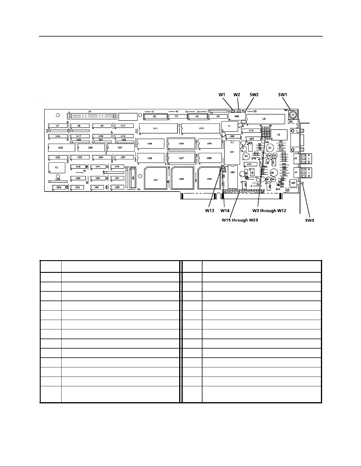
Figure A-1. Switch and Jumper Locations for 1731N Mini Link
Table A-1. Alphanumeric Listing of Jumpers and Switches for 1731N Mini Link
Ref. Function Ref. Function
SW1 Mini Link ICN Device Address W11* Select 38400 Baud on External Serial Port
SW2 Base Address of Integral Serial Port W12* Select 76800 Baud on External Serial Port
SW3 Mini Link Reset Switch W13 Select ICN Baud Rate of 62500 bps
W1 Enable CTS on External Serial Port W14 Select ICN Baud Rate of 31250 bps
W2 Enable CTS on PC/AT Serial Port W15 Select IRQ3 for Integral Serial Port
W3* Select 76800 Baud on Integral Serial Port W16 Select IRQ4 for Integral Serial Port
W4* Select 38400 Baud on Integral Serial Port W17 Select IRQ5 for Integral Serial Port
W5 Select 19200 Baud on Integral Serial Port W18 Select IRQ6 for Integral Serial Port
W6 Select 9600 Baud on Integral Serial Port W19 Select IRQ7 for Integral Serial Port
W7 RESERVED W20 Select Interrupt Polarity Logic 1
W8 RESERVED W21 Select Interrupt Polarity Logic 0
W9 Select 9600 Baud on External Serial Port W22 Enable 5V Test Signal on 9-pin RS-232
W10 Select 19200 Baud on External Serial Port W23 De-Select Isolation Feature on ICN / PC
Interface
* Software and firmware support for these baud rates is currently unavailable.
A-1
Page 24

IB-23C003
APPENDIX A - JUMPERS AND SWITCHES
Figure A-2. Switch and Jumper Locations for 1732N ICN Interface Board
Table A-2. Alphanumeric Listing of Jumpers and Switches for 1732N ICN Interface Board
Ref. Function
J2 Select ICN1 Baud Rate of 31,250 bps
J3* Select ICN1 Baud Rate of 62,500 bps
U1 Mini Link ICN1 Device Address
* Firmware support for this baud rates is currently unavailable.
A-2
Page 25

APPENDIX B - CONNECTOR DESCRIPTIONS
APPENDIX B
CONNECTOR DESCRIPTIONS
Table B-1. IBM PC/AT Mini Link Board Connector Pinout
IB-23C003
Component Side
("A" side w/A1 near rear panel)
I/O Pin Signal I/O
("B" side w/B1 near rear panel)
I/O Pin Signal I/O
Circuit Side
A1 –I/OCHCK I B1 GND GND
A2* SD7 I/O B2* RESET D O
A3* SD6 I/O B3* +5V Power
A4* SD5 I/O B4 IRQ9 I
A5* SD4 I/O B5 –5V Power
A6* SD3 I/O B6 DRQ2 I
A7* SD2 I/O B7 –12V Power
A8* SD1 I/O B8 0WS I
A9* SD0 I/O B9 +12V Power
A10 –IOCHRDY I B10* GND GND
A11* AEN O B11 –SMEMW O
A12 SA19 I/O B12 –SMEMR O
A13 SA18 I/O B13* –IOW I/O
A14 SA17 I/O B14* –IOR I/O
A15 SA16 I/O B15 –DACK3 O
A16 SA15 I/O B16 DRQ3 I
A17 SA14 I/O B17 –DACK1 O
A18 SA13 I/O B18 DRQ1 I
A19 SA12 I/O B19 –Refresh I/O
A20 SA11 I/O B20 CLK O
A21 SA10 I/O B21* IRQ7 I
A22* SA9 I/O B22* IRQ6 I
A23* SA8 I/O B23* IRQ5 I
A24* SA7 I/O B24* IRQ4 I
A25* SA6 I/O B25* IRQ3 I
A26* SA5 I/O B26 –DACK2 O
A27* SA4 I/O B27 T/C O
A28* SA3 I/O B28 BALE O
A29* SA2 I/O B29* +5V Power
A30* SA1 I/O B30 OSC O
A31* SA0 I/O B31* GND GND
C1 SBHE I/O D1 –MEMCS16 I
C2 LA23 I/O D2 –I/OCS16 I
C3 LA22 I/O D3** IRQ10 I
C4 LA21 I/O D4** IRQ11 I
C5 LA20 I/O D5** IRQ12 I
C6 LA19 I/O D6** IRQ15 I
C7 LA18 I/O D7** IRQ14 I
C8 LA17 I/O D8 –DACK0 O
C9 –MEMR I/O D9 DRQ0 I
C10 –MEMW I/O D10 –DACK5 O
C11 SD08 I/O D11 DRQ5 I
C12 SD09 I/O D12 –DACK6 O
C13 SD10 I/O D13 DRQ6 I
C14 SD11 I/O D14 –DACK7 O
C15 SD12 I/O D15 DRQ7 I
C16 SD13 I/O D16 +5V Power
C17 SD14 I/O D17 –MASTER I
C18 SD15 I/O D18 GND GND
* Currently in use by the Mini Link ** Usable by the Mini Link with minor
modification
B-1
Page 26

IB-23C003
APPENDIX B - CONNECTOR DESCRIPTIONS
Table B-2. Mini Link RS-232 Connector Pinout
I/O Pin Signal Name I/O
1 GND GND
2 RXDATA I
3 TXDATA O
4 NC -
5 GND GND
6 NC -
7 RTS I
8 CTS O
9* NC -
* Pin 9 can be configured to present Mini Link's 5VDC (for test purposes only) by using jumper W22.
Table B-3. Mini Link ICN0 and ICN1 Connector Pinout
Terminal Signal Name*
1 IBUS(+)
2 IBUS(–)
GND GND
* Two- or Three-Wire Connection for ICN0 and ICN1. The (+) and (-) terminals accept signals from the ICN. The third terminal,
labeled "GND" is used when the Isolation Feature is employed (see jumper setting for W23).
B-2
Page 27

Page 28

The Company’s policy is one of continuous product improvement and the right
is reserved to modify the information contained herein without notice, or to
make engineering refinements that may not be reflected in this bulletin.
Micromod Automation assumes no responsibility for errors that may appear in
this manual.
© 2004 MicroMod Automation, Inc. Printed in USA
IB-23C003, Issue 2 04/2005
MicroMod Automation, Inc.
75 Town Centre Drive
Rochester, NY USA 14623
Tel. 585-321 9200
Fax 585-321 9291
 Loading...