

Datasheet ML6420CS-3, ML6420CS-4, ML6420CS-5, ML6420CS-7, ML6420CS-1 Datasheet (Micro Linear Corporation)
September 1999
PRELIMINARY
ML6420*
Triple/Dual Phase-Equalized, Low-Pass Video Filter
GENERAL DESCRIPTION
The ML6420 monolithic BiCMOS 6th-order filters provide
fixed frequency low pass filtering for video applications.
These triple output phase-equalized filters are designed for
input anti-aliasing filtering.
Cut-off frequencies are either 3.0, 5.5, 8.0, or 9.3MHz.
Each channel incorporates a 6th-order low-pass filter, a
first order all-pass filter, and a 75W coax cable driver. A
control pin (Range) is provided to allow the inputs to
swing to ground by providing a 0.5V offset to
the input.
The filters are powered from a single 5V supply, and can
drive 1V
over 75W (0.5V to 1.5V), or 2V
P-P
over 150W
P-P
(0.5V to 2.5V).
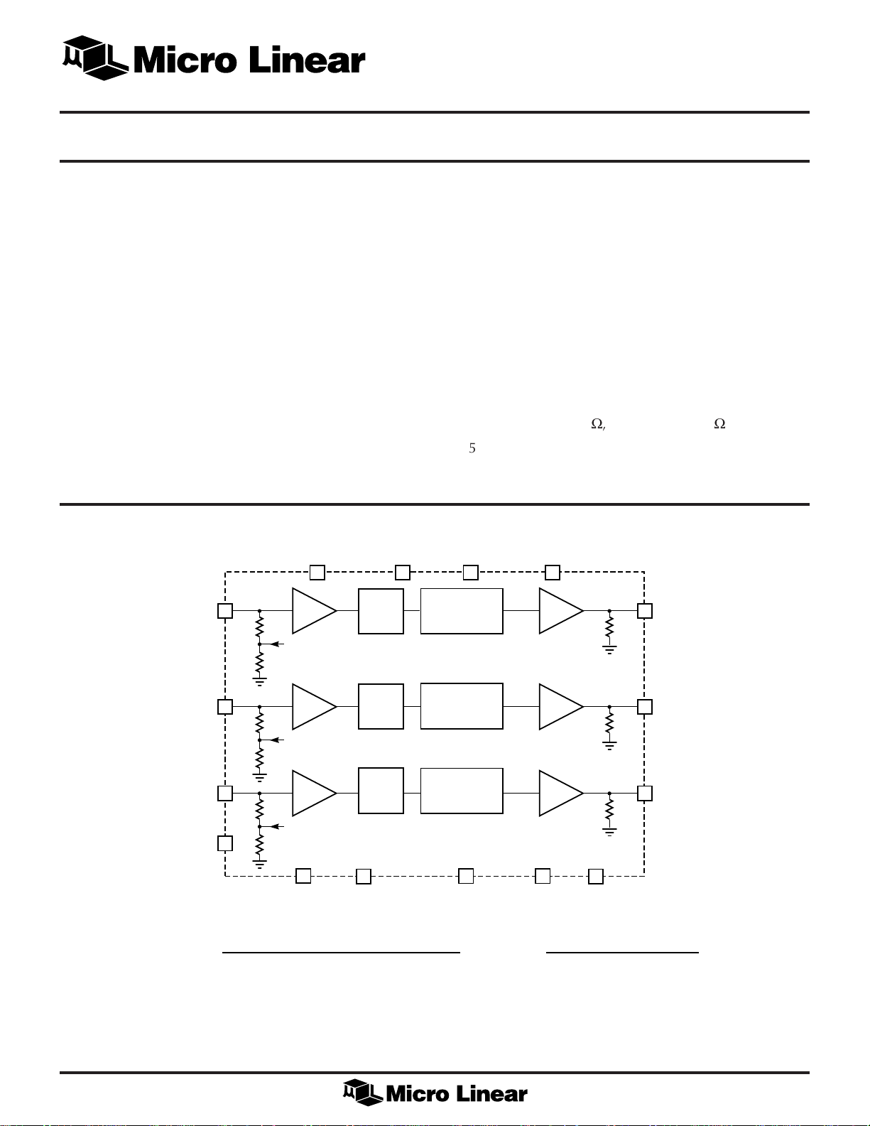
ML 6420 BLOCK DIAGRAM
V
B
CC
8
V
CC
6
FEATURES
■ 3.0, 5.5, 8.0, or 9.3 MHz bandwidth
■ 1X or 2X gain
■ 6th-order filter with equalizer
■ >40dB stopband rejection
■ No external components or clocks
■ ±10% maximum frequency accuracy over supply
and temperature
■ <2% differential gain, <2° differential phase
■ <25ns group delay variation
■ Drives 1V
■ 5V ±10% operation
■ ML6420 available with 6dB gain
* Some Packages Are End Of Life
C
V
CC
5
into 75W, or 2V
P-P
V
A
CC
11
into 150
P-P
W
V
IN
V
IN
V
IN
RANGE
15
A
3k
1k
B
16
3k
1k
2
C
3k
14
1k
I
I
I
BIAS
BIAS
BIAS
BUF
BUF
BUF
12
GND
LOW PASS
A
LOW PASS
B
LOW PASS
C
13
GNDA
ALL PASS
A
ALL PASS
B
ALL PASS
C
4
GNDC
1X/2X
BUF
1X/2X
BUF
1X/2X
BUF
1
GNDB
3
GND
3.33K
3.33K
3.33K
10
V
OUT
9
V
OUT
7
V
OUT
1X GAIN 2X GAIN
ML6420-1 ML6420-3 ML6420-4 ML6420-5 ML6420-7
FILTER A 5.5MHZ 8.0MHZ 8.0MHZ 5.5MHZ 9.3MHZ
FILTER B 5.5MHZ 8.0MHZ 3.0MHZ 2.5MHZ 9.3MHZ
FILTER C 5.5MHZ 8.0MHZ 3.0MHZ 2.5MHZ 9.3MHZ
A
B
C
Triple Input/Anti-aliasing Video Filter
1
ML6420
PIN CONFIGURATION
PIN DESCRIPTION
ML6420
16-Pin Wide SOIC (S16W)
CC
1
2
3
4
5
6
7
C
8
TOP VIEW
GNDB
VINC
GND
GNDC
VCCC
V
OUT
VCCB
V
16
VINB
15
VINA
14
RANGE
13
GNDA
12
GND
11
VCCA
10
V
A
OUT
9
V
B
OUT
PIN NAME FUNCTION
1 GNDB Ground pin for filter B
2VINC Signal input to filter C. Input
impedance is 4kW.
3 GND Power and logic ground
4 GNDC Ground pin for filter C.
5V
CC
Positive supply for bias circuit.
6VCCC Power supply voltage for filter C.
7V
C Output of filter C. Drive is 1V
OUT
75W (0.5V to 1.5V) or 2V
into 150
P-P
(0.5V to 2.5V).
8VCCB Power supply voltage for filter B.
9V
B Output of filter B. Drive is 1V
OUT
75W (0.5V to 1.5V) or 2V
into 150
P-P
(0.5V to 2.5V).
10 V
A Output of filter A. Drive is 1V
OUT
75W (0.5V to 1.5V) or 2V
into 150
P-P
(0.5V to 2.5V).
P-P
P-P
P-P
into
into
into
PIN NAME FUNCTION
11 VCCA Power supply voltage for filter A.
12 GND Power and logic ground.
13 GNDA Ground pin for filter A.
14 RANGE Input signal range select. For -1 to -4;
when RANGE is low (0), the input
signal range is 0.5V to 2.5V, with an
output range of 0.5V to 2.5V. When
RANGE is high (1) the input signal
range is 0V to 2V, with an output range
of 0.5V to 2.5V. For -5 to -12; when
RANGE is low (0), the input signal
W
range is 0.5V to 1.5V, with an output
range of 0.5V to 2.5V. When RANGE is
high (1) the input signal range is 0V to
1V, with an output range of 0.5V to
2.5V.
W
15 VINA Signal input to filter A. Input
impedance is 4kW.
16 VINB Signal input to filter B. Input
W
impedance is 4kW.
2
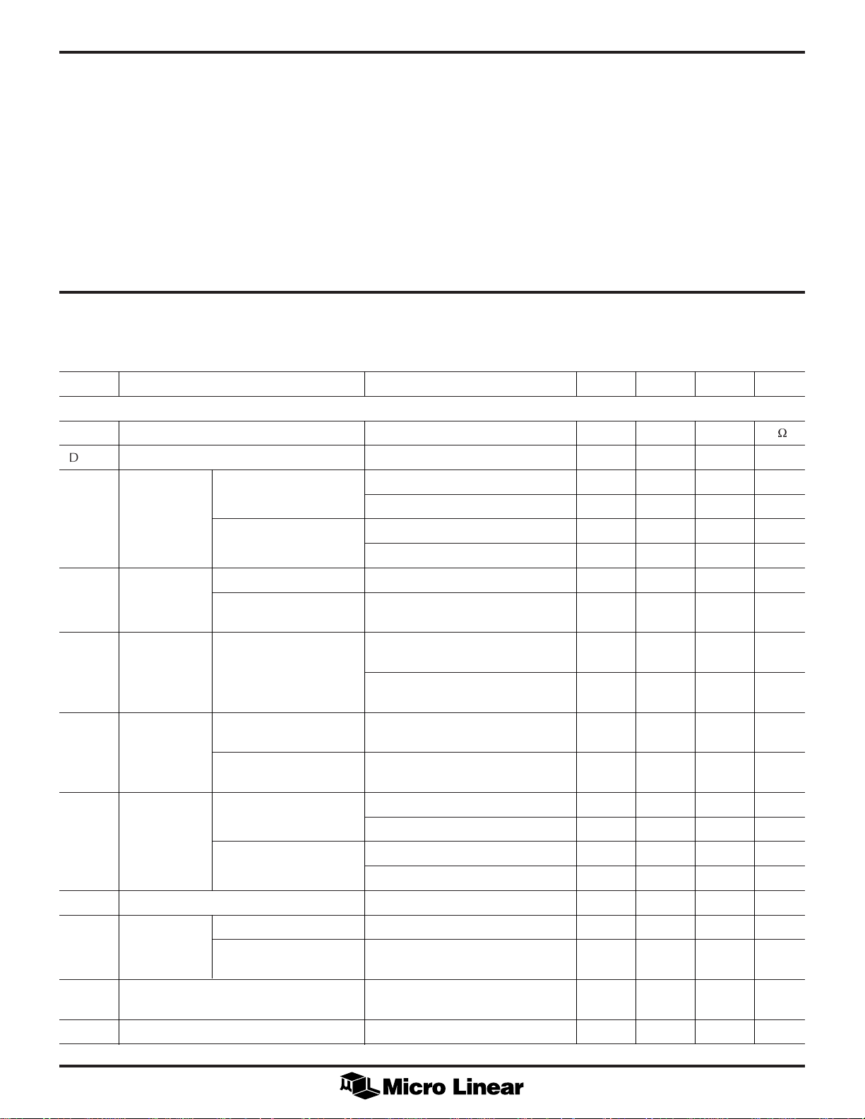
ABSOLUTE MAXIMUM RATINGS
ML6420
Absolute maximum ratings are those values beyond which
the device could be permanently damaged. Absolute
maximum ratings are stress ratings only and functional
device operation is not implied.
Supply Voltage (VCC) ...................................... –0.3 to 7V
Storage Temperature .................................. –65° to 150°C
Package Dissipation at TA = 25°C............................... 1W
Lead Temperature (Soldering 10 sec) ...................... 260°C
Thermal Resistance (qJA) ...................................... 65°C/W
OPERATING CONDITIONS
GND .................................................. –0.3 to VCC +0.3V
Logic Inputs......................................... –0.3 to VCC +0.3V
Input Current per Pin ............................................±25mA
Supply Voltage ................................................. 5V ± 10%
Temperature Range ........................................0°C to 70°C
ELECTRICAL CHARACTERISTICS
Unless otherwise specified, VCC = 5V ± 10%, TA = Operating Temperature Range, RL =75W or 150W, V
150W Load and V
SYMBOL PARAMETER CONDITIONS MIN TYP MAX UNITS
GENERAL
R
DR/R
I
BIAS
Input Impedance 3 4 5 k
IN
Input R Matching Between filters A, B and C ±2 %
IN
Input Current ML6420 (–1 to –4) VIN = 0.5V, range = low –80 µA
OUT
= 1V
for 75W Load (Notes 1-3)
P-P
VIN = 0.0V, range = high –125 µA
OUT
= 2V
P-P
for
W
ML6420 VIN = 0.5V, range = low 45 µA
(–5 to–7) VIN = 0.0V, range = high –210 µA
Small Signal ML6420 (–1 to –4) VIN = 100mV
Gain ML6420 VIN = 100mV
(–5 to –7)
Differential ML6420 (–1 to –4) V
Gain ML6420 V
(–5 to –7)
Differential ML6420 (–1 to –4) VIN = 1.8V ± 0.7V at 1 deg
Phase ML6420 VIN = 0.8V to 1.5V 1 deg
(–5 to –7)
V
Input Range ML6420 (–1 to –4) RANGE = 0, Ground 0.5 2.5 V
IN
ML6420 RANGE = 0, Ground 0.5 1.5 V
(–5 to –7) RANGE = 1, V
Peak Overshoot 2T, 0.7V
Crosstalk ML6420 (–1 to –4) fIN = 3.58, fIN = 4.43MHz 50 dB
= 1.8V ± 0.7V at 1 %
IN
3.58 & 4.43 MHz
= 0.8V to 1.5V 1 %
IN
3.58 & 4.43 MHz
RANGE = 1, V
at 100kHz –0.5 0 0.5 dB
P-P
at 100kHz 5.5 6 6.5 dB
P-P
CC
CC
pulse 2.0 %
P-P
0.0 2.0 V
0.0 1.0 V
ML6420 fIN = 3.58, fIN = 4.43MHz 45 dB
(–5 to –7)
Channel to Channel fIN = 100kHz ±10 ns
Group Delay Matching (fC = 5.5MHz) Filters with identical f
Channel to Channel Gain Matching fIN = 100kHz ±2 %
C
3
ML6420
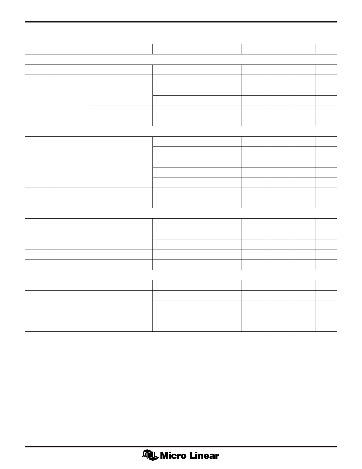
ELECTRICAL CHARACTERISTICS (Continued)
SYMBOL PARAMETER CONDITIONS MIN TYP MAX UNITS
GENERAL (Continued)
Output Current RL = 0 (short circuit) 75 mA
C
3.0/3.3MHZ FILTER – ML6420
5.50MHZ FILTER – ML6420-1
Load Capacitance 35 pF
L
Composite ML6420 (–1 to –4) fC = 5.5MHz ±10 ns
Chroma/Luma fC = 8.0MHz ±8 ns
Delay At 3.58 ML6420 (–5 to –7) fC = 5.5MHz ±15 ns
& 4.43MHz fC = 9.3MHz ±8 ns
Bandwidth (monotonic passband) –3dB (3.0MHz) 2.7 3.0 3.3 MHz
Stopband Attenuation fIN = 9.82MHz (3.0MHz) 30 33 dB
Output Noise BW = 30MHz 490 µV
Group Delay 225 ns
Bandwidth (monotonic passband) –3dB 4.95 5.50 6.05 MHz
Stopband Attenuation fIN = 10MHz 16 18 dB
–3dB (3.3MHz) 3.0 3.3 3.6 MHz
fIN = 9.82MHz (3.3MHz) 35 40 dB
fIN = 60MHz 43 50 dB
RMS
fIN = 50MHz 40 45 dB
Output Noise BW = 30MHz 700 µV
Group Delay 145 ns
8.0MHZ FILTER – ML6420
Bandwidth (monotonic passband) –3dB 7.2 8.0 8.8 MHz
Stopband Attenuation fIN = 17MHz 20 25 dB
Output Noise BW = 30MHz 700 µV
Group Delay 120 ns
RMS
fIN = 85MHz 40 42
RMS
4

ML6420
ELECTRICAL CHARACTERISTICS (Continued)
SYMBOL PARAMETER CONDITIONS MIN TYP MAX UNITS
5.50MHZ FILTER – ML6420-5
Bandwidth (monotonic passband) –3dB (Note 5) 4.95 5.50 6.05 MHz
Attenuation fIN = 10MHz 20 25 dB
fIN = 50MHz 45 55 dB
Output Noise BW = 30MHz 1 mV
Group Delay 170 ns
Small Signal Gain V
= 100mV
IN
at 100kHz, 5.5 6 6.5 dB
P-P
Filter A or C
CV Composite Small Signal Gain VINA, C = 100mV
at 100kHz 11 12 13 dB
P-P
9.3MHZ FILTER – ML6420-7
Bandwidth (monotonic passband) –3dB (Note 5) 8.4 9.3 10.2 MHz
Attenuation fIN = 17MHz 20 25 dB
fIN = 85MHz 45 55 dB
Output Noise BW = 30MHz 1 mV
Group Delay 100 ns
DIGITAL AND DC
V
V
I
I
Logic Input Low RANGE 0.8 V
IL
Logic Input High RANGE VCC – 0.8 V
IH
Logic Input Low VIN = GND –1 µA
IL
Logic Input High VIN = V
IL
CC
1µA
ICCSupply Current RL = 75W VIN = 0.5V (Note 4) 110 135 mA
VIN = 1.5V 150 175 mA
RMS
RMS
Note 1: Limits are guaranteed by 100% testing, sampling, or correlation with worst case test conditions.
Note 2: Maximum resistance on the outputs is 500W in order to improve step response.
Note 3: Connect all ground pins to the ground plane via the shortest path.
Note 4: Power dissipation P
Note 5: The bandwidth is the –3dB frequency of the unboosted filter. This represents the attenuation that results from boosting the gain from -3dB point at the
specified frequency.
= (ICC ´ VCC) – [3 (V
D
OUT
2
/RL)]
5
ML6420
FUNCTIONAL DESCRIPTION
The ML6420 single-chip Dual/Triple Video Filter ICs are
intended for low cost professional and consumer video
applications. Each channel incorporates an input buffer
amplifier, a sixth order lowpass filter, a first order allpass
equalizer, and an output 1X or 2X gain amplifier capable
of driving 75W to ground.
When RANGE is low the input and output signal range is
0.5V to 1.5V. When the input signal range is 0V to 1V,
RANGE should be tied high. In this case, an offset is added
to the input so that the output swing is kept between 0.5V
to 1.5V. The output amplifier is capable of driving up to
24mA of peak current; therefore the output voltage should
not exceed 1.8V when driving 75W to ground. The
ML6420 can be driven by a DAC with swing down to 0V.
The summer output on the ML6422 is given by 2x(V
V
) – 2.5V when RANGE = 0 and 2x(V
INC
0.5V when RANGE is high. So, V
such that this output does not go below 0.5V or above
2.5V for proper operation.
INA
and V
INA
INC
+ V
should be
INC
INA
) –
+
6

APPLICATION GUIDELINES
ML6420
OUTPUT CONSIDERATIONS
The triple filters have unity or 2X gain. The output circuit
has unity or 2X gain (0dB) when connected to a 150
load, and a –6dB gain when driving a 75W load via a 75
series output resistor. The output may be either AC or DC
coupled. For AC coupling (Figure 6), the –3dB point
should be 5Hz or less. There must also be a DC path of
£
500W to ground for biasing.
The dual filters have 2X gain. The filter has 2X gain (6dB)
when connected to a 150W load, and a 0dB gain when
driving a 75W load via a 75W series output resistor. The
output may be either AC or DC coupled. For AC coupling,
the –3dB point should be 5Hz or less. There must also be a
DC path of £500W to ground for output biasing.
INPUT CONSIDERATIONS
The input resistance is 4kW. The input may be either DC or
AC coupled. (Note that each input sources 80 to 125µA of
bias current).
LAYOUT CONSIDERATIONS
In order to obtain full performance from these triple filters,
layout is very important. Good high frequency decoupling
is required between each power supply and ground.
Otherwise, oscillations and/or excessive crosstalk may
occur. A ground plane is recommended.
Each filter has its own supply and ground pins. In the test
circuit, 0.1µF capacitors are connected in parallel with
0.001µF capacitors on pins VCC, VCCA, VCCB and VCCC for
maximum noise rejection (Figure 6A and Figure 1G).
Further noise reduction is achieved by using series ferrite
beads. In typical applications, this degree of bypassing
W
W
may not be necessary.
Since there are three filters in one 16-pin SOIC package,
space the signal leads away from each other as much
as possible.
POWER CONSIDERATIONS
The ML6420 power dissipation follows the formula:
2
V
PI V
=× ×
16
DCCCC
This is a measure of the amount of current the part sinks
(current in — current out to the load).
Under worst case conditions:
PmW
=× ×
..–
05
D
Power consumption can be reduced by not suppling V
to unused filter sections. (VCCA, VCCB or VCCC)
TEST CIRCUITS
Figures 6A shows the test circuitn used for measuring the
frequency and group delay. It is expected that actual
customer circuits will be much simpler, since board
bypasses already exist and DC coupling or clamping will
be utilized at the inputs.
OUT
–
R
15
.
75
3
L
2
=0175 55
3 8725
.
CC
ML6420 VIDEO LOW PASS FILTER
Filter Selection: The ML6420 provides several choices in
filter cut-off frequencies depending on
the application.
7

ML6420
RGB: When the bandwidth of each signal is the same,
then the 5.5MHz or 8.0MHz/9.3MHz are appropriate
depending on the sampling rate. (13.5MHz vs 27MHz)
filtering for 4.2MHz, 5.0MHz.
YUV: When the luminance bandwidth is different from the
color bandwidth, the ML6420-4 with the 8.0, 3.0 and
3.0MHz filters are more appropriate.
S-Video: For Y/C (S-video) and Y/C + CV (Composite
Video) systems the ML6420 with 5.5MHz or 8.0MHz
filters or ML6422 with 5.5MHZ and 9.3MHz filters are
appropriate. In NTSC the C signal occupies the bandwidth
from about 2.6MHz to about 4.6MHz, while in PAL the C
signal occupies the bandwidth from about 3.4MHz to
about 5.4MHz. In both cases, a 5.5MHz low pass filter
provides adequate rejection for both sampling and
reconstruction. In addition, using the same filter for both Y/
C and CV maintains identical signal timing
without adjustments.
Composite: When one or more composite signals need to
be filtered, then the 5.50MHz, 8.0MHz, or 9.3MHz filters
permit filtering of one, two or three composite signals.
4X Over sampling: While the ML6420 filters can eliminate
the need for over sampling combined with digital filtering,
there are times when over sampling is needed. For these
situations, 8.0MHz or 9.3MHz is used in place of
5.5MHz, and 3.0MHz is used in place
of 1.8MHz.
Sinx/x: For digital video system with output D/A converters,
there is a fall-off in response with frequency due to discrete
sampling. The fall-off follows a sinx/x response. The ML6421
and ML6423 filters have a complementary boost to provide
a flatter overall response. The boost is designed for 13.5MHz
and 27MHz Y/C and CV sampling and 6.75MHz or
13.5MHz U/V sampling. The ML6421 has the same pin-out
as the ML6420.
TYPICAL CLAMPING SCHEMES
Figures 8 and 9 show two typical applications of the
ML6420 for anti-aliasing prior to A-to-D conversion. In
Figure 8, a single precision digital feedback clamp circuit
includes both the ADC and the ML6420. This establishes
the proper DC operating point for the ML6420 (with
RANGE input = 0V, 0.5V £ VIN £ 1.5V; with RANGE input
= 5V, 0.0 £ VIN £ 1.0V.) and the ADC. Figure 8 is typically
used with ADC’s that require external clamp circuitry.
Figure 9 shows AC coupled application for ADC’s with
built-in clamps. In this case, the clamp is internal to the
ADC and the ML6420 uses a simple coarse clamp at its
input to establish the proper operating point.
USING VIDEO FILTERS
NTSC/PAL: A 5.50MHz cut-off frequency provides good
The ML6420 are monolithic, triple/dual lowpass filters
intended for input anti-aliasing prior to analog to digital
conversion in video systems.
8

ALIASING: THE PROBLEM
ML6420
Aliasing is a signal distorting process that occurs when an
analog signal is sampled. If the analog signal contains
frequencies greater than half of the sampling rate, those
frequencies will be altered and “folded back” in the
frequency domain. These frequencies represent a distortion
of the original signal as represented in the sampled domain,
and cannot be corrected after sampling.
THE RESULT OF ALIASING IN A TV PICTURE
Aliasing causes several disturbing distortions to a picture.
Since the folded spectrum adds to the original spectrum, it
will sometimes be in phase, and sometimes out of phase
causing ripples in response that depend on the position of
the picture element relative to the clock. The net effect is
that picture elements, edges, highlights, and details will
“wink” in amplitude as they move across a picture if they
have high frequency content above the Nyquist frequency
of the sampler.
ANTI-ALIASING
Anti-aliasing reduces the bandwidth of the signal to a
value appropriate for the sample processing system. Some
detail information is lost, but only the information that
cannot be unambiguously displayed is removed. Assuming
that the passband contains the “real” picture information,
the only distortion that occurs is due to amplitude and
phase variations of the anti-aliasing filter in the passband.
The following section shows approaches using digital and
analog filters in an oversampled system, and a monolithic
analog filter as a lower cost alternative.
OVERSAMPLING
Aliasing cannot be removed once it occurs, it must be
prevented at the signal sampler. Many current systems are
choosing to prevent aliasing by increasing the clock rate of
the sampler. This is known as “oversampling”. Doubling
the clock rate greatly reduces the burden on the analog
anti-alias filter, but the increased data rate greatly
increases the size, complexity and cost of the Digital
Signal Processing (DSP) circuitry. Since the higher clock
rate generates more samples than are necessary to
represent the desired passband content, a digital filter may
be used to decimate the signal back to a lower sample
rate, saving size, complexity and power in the
downstream circuitry. Since this digital filter itself is a
complex digital block, this method cannot be considered
the lowest cost approach to solving the anti-alias problem.
NYQUIST SAMPLING
In traditional systems, before the advent of higher speed
ADCs, anti-aliasing filters were designed in the analog
domain. The movement toward higher sampling rates was
an attempt to circumvent the difficult challenge of
designing a sharp roll-off, linear phase, non-distorting
analog filter. The ML6420 series of filters solve this
problem where it is best solved, in the analog domain.
Since they are monolithic, their application is simple.
Since they have flat amplitude and linear phase, they are
low distortion. And since the aliasing is removed at the
analog input to the ADC, the clock rates are minimized,
an expensive DSP half band filter is eliminated, and
significant power is conserved.
Oversampling vs Nyquist sampling
Clearly the purely analog monolithic solution versus the
analog/digital solution using DSP filtering are different
ways of solving the same problem. Other than costs
(purely analog is many times less expensive) there are no
real differences in performance for applications that
require flatness specs of ±0.5db to 4.5MHz for consumer
and pro-sumer video applications. The ML6420/ML6422
are also phase corrected for flat group delay, a feature not
found in typical low cost analog filters, and a
characteristic often associated with digital filters alone.
The following section highlights the importance of linear
phase response in video applications.
TIME DOMAIN RESPONSE:
TRANSIENTS AND RINGING
The phase response of filters is often ignored in
applications where time domain waveforms are not
relevant. But in video applications the time domain
waveform is the signal that is finally presented on the
screen to the viewer, and so time domain characteristics
such as pulse response symmetry, pre-shoot, over-shoot
and ringing are very important. Video applications are
very demanding in that they require both sharp cutoff
characteristics and linear phase. The application of DSP to
the problem is based on the linear phase characteristic of
a particular class of digital filters known as symmetrical
FIR filters. Use of these filters guarantees the best possible
time domain characteristics for a given amplitude
characteristic. In the analog domain phase linearity is not
automatic (except for special phase linear filters such as
Bessel or Thomson filters, both of which have inadequate
amplitude characteristics for most video anti-alias
applications) and it is often assumed that linear phase is
unachievable. This is not true. Similarly, in the digital
domain it is often assumed that sharp cutoff amplitude
characteristics can be achieved without overshoot and
ringing. This is also not true. Phase linear filters whether
digital or analog have symmetrical response to
symmetrical inputs. High roll-off rate uncompensated
filters (whether analog or digital) have ringing and
overshoot. In the example below, the traditional 2T test
pulse is applied to a traditional, non-phase linear analog
filter, the ML6420 pure analog anti-alias filter (5.5MHz)
and the combined analog/digital filters (9.3MHz analog
filter and half-band digital filter.)
As seen in Figure 19c, the ML6420 filters provide a time
domain response that is comparable to more complex and
expensive filters.
Typical Passive Filter
9

ML6420
USING VIDEO FILTERS (CONTINUIED)
The output waveform is not symmetric. All ringing occurs
after the main pulse. Result is visual smearing and fine
ghosting to the right of every edge in the picture. See old
Figure 19a.
Phase Corrected Analog Filter
Output waveform is substantially symmetric. Ringing is
greatly reduced. Result is increase in apparent resolution.
No smearing or ghosting.
Analog Filtering in the Time Domain
Output waveform is symmetric. Ringing is about the same
as ML6420 alone. Difference between purely analog and
analog/digital approach is subtle and will only have a
material effect on multi-pass video processing.
TYPICAL ANALOG FILTER
Figure 19a.
ML6420
5.5MHz TYP
Figure 19b.
DIGITAL FILTER
HALF-BAND
10
Figure 19c.

10
0
–10
–20
–30
–30
–40
–50
–60
RELATIVE AMPLITUDE (dB)
–70
–80
–90
100k 1M 10M 100M
FREQUENCY (Hz)
Figure 1A. Stop-Band Amplitude vs Frequency
(fC = 5.5MHz). ML6420
Note: Figure 1, 2 and 3 data was measured using the test circuit in Figure 6.
+1
+0.25
0
–0.5
–1.25
–2.0
–2.75
–3.5
–4.25
RELATIVE AMPLITUDE (dB)
–5.0
–5.75
–6.5
100k 1M 10M
FREQUENCY (Hz)
Figure 2A. Pass-Band Amplitude vs Frequency
(fC = 5.5MHz). ML6420
ML6420
ML6420-1
GROUP DELAY (10ns/Div)
ML6420-5
2M 7M
FREQUENCY (Hz)
Figure 3A. Group Delay vs Frequency (fC = 5.5MHz).
ML6420
11

ML6420
+3
+2
+1
0
–1
–2
–3
–4
–5
–6
–7
AMPLITUDE (dB)
FREQUENCY (Hz)
100k 1M 10M
GROUP DELAY (10ns/Div)
FREQUENCY (Hz)
100K 5M
+5
0
–5
–10
–15
–20
–25
AMPLITUDE (dB)
–30
–35
–40
–45
100k 1M 10M
FREQUENCY (Hz)
Figure 1C. Stop-Band Amplitude vs Frequency
(fC = 9.3MHz). ML6420
+3
+2
+1
0
+10
0
–10
–20
–30
–40
–50
AMPLITUDE (dB)
–60
–70
–80
–90
100k 1M 10M
FREQUENCY (Hz)
Figure 1D. Stop-Band Amplitude vs Frequency
(fC = 3MHz). ML6420
–1
–2
–3
AMPLITUDE (dB)
–4
–5
–6
–7
100k 1M 10M
Figure 2C. Pass-Band Amplitude vs Frequency
GROUP DELAY (10ns/Div)
FREQUENCY (Hz)
(fC = 9.3MHz). ML6420
ML6420-7
ML6420-3
Figure 2D. Pass-Band Amplitude vs Frequency
(fC = 3MHz). ML6420
12
1M 11M
FREQUENCY (Hz)
Figure 3C. Group Delay vs Frequency (fC = 9.3MHz).
ML6420
Figure 3D. Group Delay vs Frequency (fC = 3MHz).
ML6420

Figure 1H. Cascading Filters for Sharper Cutoff
ML6420
Figure 4. Burst with 100ns Pulse and Fast Transition at
ML6420 Output Showing Symetrical Pulse Response
Note: Figure 4 and 5 data was measured using the test circuit in Figure 7.
Figure 5. Step with 2T and 12T Response at ML6420
Output Showing Accurate Pulse Response without
Overshoot or Ringing
13

ML6420
+5V
0.001µF
0.1µF
INC
INPUT SIGNAL = 2V
OUTC
100µF
P-P
75Ω
COUPLING
0.1µF
85Ω
FB2
INPUT
100µF
INPUT
TERMINATION
FB1
DC
BIAS
SUPPLY NOISE
CLAMPING
47Ω
1µF
3.1kΩ
1kΩ
1nF
0.1µF
1nF
0.1µF
1nF
0.1µF
1
2
3
4
5
6
7
8
GNDB
V
C
IN
GND
GNDC
V
CC
VCCC
V
OUT
V
B
CC
47Ω
0.1µF
3.1kΩ
16
V
B
IN
15
V
A
IN
14
RANGE
13
GNDA
1nF
12
GND
11
V
A
CC
10
V
V
OUT
OUT
A
9
B
C
1µF
100µF
1kΩ
0.1µF
100µF
0.1µF
75Ω
75Ω
85Ω
47Ω
INB
3.1kΩ
1kΩ
1µF
INA
85Ω
OUTA
OUTB
14
Figure 6A. ML6420 AC Coupled DC Bias Test Circuit

ML6420
+5V
COARSE CLAMP
1K
VIDEO
INPUT
OPTIONAL 6dB GAIN
1V
P-P
+
220µF
0.1µF
2N3904
100Ω
75Ω
1µF
47k
2.5k
+5V
0.1µF
AD847(5V)
+
–
–5V
0.1µF
R
G
2.5k
GAIN = 1 +
2N3904
131Ω
R
G
2.5k
100Ω
Figure 7. Video Clamp Prior to A/D Conversion
INPUT
5V
1/3 ML6420
1/2 ML6422
OUTPUT
RANGE
A/D
150Ω
15

ML6420
ANALOG VIDEO
ANALOG VIDEO
INPUT
INPUT
PRECISION CLAMP CIRCUITRY (MAY BE IN ADC MODULE)
ML6420/ML6422
ANTI-ALIAS FILTER
DIGITAL CLAMP:
COMPARATOR
Figure 8. DC Coupled Video Digitizer for 2V
V
≥200µF
CC
ML6420/ML6422
ANTI-ALIAS FILTER
≤500
≤500
REF LEVEL
ADC
Video Signals
P–P
ADC
DIGITAL VIDEO
8
OUTPUT
8
DIGITAL VIDEO
OUTPUT
16
DIGITAL CLAMP:
COARSE CLAMP
CIRCUITRY
PRECISION CLAMP CIRCUITRY (MAY BE IN ADC)
COMPARATOR
Figure 9. AC Coupled Video Digitizer for 2V
REF LEVEL
Video Signals
P–P

ML6420
ANALOG IN
ADC
SIGNAL
PROCESSING
Fs CLOCK
DAC
ANALOG OUT
Figure 10. Simplified Digital Video Processing System
DESIRED PASSBAND
SIGNAL CONTENT
DISTORTION FROM
“FOLDED” FREQUENCIES
0Hz Fs/2 Fs
SIGNAL CONTENT AT
FREQUENCIES > Fs/2
Figure 11. Aliasing in the Frequency Domain
ELEMENTS THAT
ARE “OFF” THE
CLOCK WILL
BE MISSED
TYPICAL SAMPLING
CLOCK
HIGH FREQUENCY
ELEMENTS THAT
ARE “ON” THE
CLOCK WILL BE
SAMPLED 100%
0 t
Figure 12. Aliasing in the Time Domain
17

ML6420
ANALOG IN
ADC
ML6420
9.3MHz TYP
DIGITAL FILTER
Figure 13. Oversampled Video Processing System with
Analog LPF & Half-Band Digital Filter
ANALOG FILTER REDUCES
ERRORS FROM F
DESIRED PASSBAND
SIGNAL CONTENT
0Hz F
DSP FILTER REDUCES
ERRORS FROM F
TO F
OUTPUT OF
F0/2 2xF
0
AT THE
0
THE ADC
/2
Figure 14. Digital Filtering in the Frequency Domain
HALF-BAND
F0 CLOCKx2
TO 2xF
AT THE INPUT OF
0
0
THE ADC
SIGNAL
PROCESSING
0
ANALOG/DIGITAL COMBO
YIELDS LOW ALIASING
ERRORS
DAC
ANALOG OUT
0
HIGH FREQUENCY ELEMENTS THAT ARE REDUCED IN AMPLITUDE
AND BROADENED TO COVER MORE THAN 1 PIXEL.
SAMPLING CLOCK
AT OUTPUT
0 t
Figure 15. Digital Filtering in the Time Domain
18

ML6420
ANALOG IN
0Hz F0/2 F
ADC
ML6420
5.5MHz TYP
SIGNAL
PROCESSING
F0 CLOCK
Figure 16. Video Processing System with
Monolithic Analog Anti-Alias Filter
ML6420/ML6422 FILTER ROLLS-OFF
ALL ERRORS ABOVE F
DESIRED PASSBAND
SIGNAL CONTENT
ALIASING ELIMINATED
WITHOUT INCREASING
CLOCK RATES
Figure 17. Analog Filtering in the Frequency Domain
DAC
/2
0
ANALOG OUT
0
ML6420/ML6422 ACHIEVES VIRTUALLY
SAME RESULTS AS DSP FILTERS.
SAMPLING CLOCK
AT OUTPUT
0 t
Figure 18. Analog Filtering in the Time Domain
19

ML6420
PHYSICAL DIMENSIONS inches (millimeters)
Package: S16W
16-Pin Wide SOIC
0.400 - 0.414
16
(10.16 - 10.52)
0.024 - 0.034
(0.61 - 0.86)
(4 PLACES)
0.090 - 0.094
(2.28 - 2.39)
1
PIN 1 ID
0.050 BSC
(1.27 BSC)
0.012 - 0.020
(0.30 - 0.51)
0.291 - 0.301
(7.39 - 7.65)
0.095 - 0.107
(2.41 - 2.72)
SEATING PLANE
0.398 - 0.412
(10.11 - 10.47)
0.005 - 0.013
(0.13 - 0.33)
0º - 8º
0.022 - 0.042
(0.56 - 1.07)
0.009 - 0.013
(0.22 - 0.33)
ORDERING INFORMATION
PART NUMBER BW (MHZ) GAIN TEMPERATURE RANGE PACKAGE
ML6420CS-1 (EOL) 5.5/5.5/5.5 1X 0°C to 70°C 16-pin SOIC (S16W)
ML6420CS-3 8.0/8.0/8.0 1X 0°C to 70°C 16-pin SOIC (S16W)
ML6420CS-4 (EOL) 8.0/3.0/3.0 1X 0°C to 70°C 16-pin SOIC (S16W)
ML6420CS-5 (EOL) 5.0/5.0/5.0 2X 0°C to 70°C 16-pin SOIC (S16W)
ML6420CS-7 (EOL) 9.3/9.3/9.3 2X 0°C to 70°C 16-pin SOIC (S16W)
Micro Linear makes no representations or warranties with respect to the accuracy, utility, or completeness of the contents of this publication
and reserves the right to make changes to specifications and product descriptions at any time without notice. No license, express or
implied, by estoppel or otherwise, to any patents or other intellectual property rights is granted by this document. The circuits contained
in this document are offered as possible applications only. Particular uses or applications may invalidate some of the specifications and/
or product descriptions contained herein. The customer is urged to perform its own engineering review before deciding on a particular
application. Micro Linear assumes no liability whatsoever, and disclaims any express or implied warranty, relating to sale and/or use of
Micro Linear products including liability or warranties relating to merchantability, fitness for a particular purpose, or infringement of any
intellectual property right. Micro Linear products are not designed for use in medical, life saving, or life sustaining applications.
© Micro Linear 2000. is a registered trademark of Micro Linear Corporation. All other trademarks are the property of their
respective owners.
Products described herein may be covered by one or more of the following U.S. patents: 4,897,611; 4,964,026; 5,027,116; 5,281,862;
5,283,483; 5,418,502; 5,508,570; 5,510,727; 5,523,940; 5,546,017; 5,559,470; 5,565,761; 5,592,128; 5,594,376; 5,652,479;
5,661,427; 5,663,874; 5,672,959; 5,689,167; 5,714,897; 5,717,798; 5,742,151; 5,747,977; 5,754,012; 5,757,174; 5,767,653;
5,777,514; 5,793,168; 5,798,635; 5,804,950; 5,808,455; 5,811,999; 5,818,207; 5,818,669; 5,825,165; 5,825,223; 5,838,723;
5.844,378; 5,844,941. Japan: 2,598,946; 2,619,299; 2,704,176; 2,821,714. Other patents are pending.
2092 Concourse Drive
San Jose, CA 95131
Tel: (408) 433-5200
Fax: (408) 432-0295
www.microlinear.com
20
DS6420-01
 Loading...