

Page 1

ML6429
75Ω Quad Video Cable Drivers and Filters
with Switchable Inputs
GENERAL DESCRIPTION
The ML6429 is a quad 4th-order Butterworth lowpass
reconstruction filter plus quad video amplifier optimized
for minimum overshoot and flat group delay. Each filter
channel has a two-input multiplexer that switches between
two groups of quad video signals. Applications driving
SCART and EVC cables are supported for composite,
component, and RGB video.
1V
input signals from DACs are AC coupled into the
P-P
ML6429, where they are DC restored. Outputs are AC
coupled, and drive 2V
can be used with DC coupled outputs for certain
applications.
A fifth unfiltered channel is provided to support an
additional analog composite video input. A swapping
multiplexer between the two composite channels allows
the distribution amplifiers to output from either input.
Several ML6429s can be arranged in a master-slave
configuration where an external sync can be used for CV
and RGB outputs.
into a 150Ω load. The ML6429
P-P
FEATURES
■ Cable drivers for Peritel (SCART), Enhanced Video
Connector (EVC), and standard video connectors, 75Ω
cable drivers for CV, S-video, and RGB
■ 7.1MHz cutoffs CV, RGB, and S-video, NTSC or PAL
filters with mux inputs and output channel mux
■ 7.1MHz to 8.4MHz cutoffs achievable with peaking
capacitor
■ Quad 4
■ 41dB stopband attenuation at 27MHz, 0.5dB flatness
up to 4.5MHz
■ 12ns group delay flatness up to 10MHz
■ 0.4% differential gain, 0.4º differential phase on all
channels, 0.4% total harmonic distortion on all channels
■ 2kV ESD guaranteed
■ Master-slave configuration allows up to 8 multiplexed,
filtered output signals
th
-order reconstruction or dual anti-aliasing filter
BLOCK DIAGRAM
/Y1*
A/Y2*
B/Y3*
REQUIRED
SYNC STRIP
MUX
MUX
MUX
MUX
CV
2
SYNCIN
23
SYNCOUT
24
CV
3
CV
4
RINA/Y4
7
RINB/Y5
8
GINA/Y6
9
GINB/Y7
10
BINA/C1
11
BINB/C2
12
A/B MUX
1
INF
INU
INU
FILTERED CHANNEL
SYNC
TIMER
SYNC
TIMER
TRANSCONDUCTANCE
TRANSCONDUCTANCE
TRANSCONDUCTANCE
TRANSCONDUCTANCE
*CAN ALSO INPUT SYNC ON GREEN SIGNALS
ERROR AMP
ERROR AMP
ERROR AMP
ERROR AMP
4th-ORDER
FILTER
TRANSCONDUCTANCE
ERROR AMP
17
0.5V
FILTER
FILTER
FILTER
RGB
V
CCO
V
CCO
+
–
+
–
0.5V
+
–
0.5V
+
–
0.5V
+
–
0.75V
4th-ORDER
4th-ORDER
4th-ORDER
CV22V
6
CC
GNDO
19
SWAP
MUX
SWAP CVF
GND
5
×2
×2
×2
×2
×2
14
13
CV
OUT
CV
OUT
R
OUT/YOUT
G
OUT/YOUT
B
SWAP CVU
1/Y
OUT
2/Y
OUT
OUT/COUT
A
21
B
20
C
18
D
16
15
REV. 1.1 2/8/2001
Page 2

ML6429
PIN CONFIGURATION
A/B MUX
CV
CV
INU
CV
INU
RINA/Y4
RINB/Y5
GINA/Y6
GINB/Y7
BINA/C1
BINB/C2
INF
/Y1
A/Y2
B/Y3
GND
V
CC
ML6429
24-Pin SOIC (S24)
1
2
3
4
5
6
7
8
9
10
11
12
TOP VIEW
24
23
22
21
20
19
18
17
16
15
14
13
SYNCOUT
SYNCIN
V
CV
CCO
CV
1/Y
OUT
CV
2/Y
OUT
GNDO
R
OUT/YOUT
V
RGB
CCO
G
OUT/YOUT
B
OUT/COUT
SWAP CVF
SWAP CVU
OUT
OUT
C
A
B
D
PIN DESCRIPTION
PIN NAME FUNCTION
1A/B MU X Logic input pin to select between Bank
<A> or <B> of the CV, RGB, or Y/C
inputs. Internally pulled high.
2CV
3CV
4CV
/Y1 Filtered analog composite video or
INF
luma video input.
A/Y2 Unfiltered analog composite video or
INU
luma video input for Bank <A>.
A composite or luma or green signal
must be present on CV
CV
B/Y3 inputs to provide
INU
INU
A/Y2 or
necessary sync signals to other
channels (R,G,B,Y,C). Otherwise, sync
must be provided at SYNCIN. For RGB
applications, the green channel with
sync can be used as an input to this
pin. (see RGB Applications section)
B/Y3 Unfiltered analog composite video or
INU
luma video input input for Bank <B>.
A composite or luma or green signal
must be present on CV
CV
B/Y3 inputs to provide
INU
INU
A/Y2 or
necessary sync signals to other
channels (R,G,B,Y,C). Otherwise, sync
must be provided at SYNCIN. For RGB
applications, the green channel with
sync can be used as an input to this
pin. (see RGB Applications section)
PIN NAME FUNCTION
5 GND Analog ground
6V
CC
Analog 5V supply
7RINA/Y4 Filtered analog RED video or luma
video input for Bank <A>
8RINB / Y5 Filtered analog RED video or luma
video input for Bank <B>
9GINA/Y6 Filtered analog GREEN video or
luma video input for Bank <A>
10 GINB/Y7 Filtered analog GREEN video or
luma video input for Bank <B>
11 BINA/C1 Filtered analog BLUE video or
chroma video input for Bank <A>
12 BINB/C2 Filtered analog BLUE video or
chroma video input for Bank <B>
13 SWAP CVU Logic input pin to select whether
the outputs of CV
CV
OUT
2/Y
OUT
1/Y
OUT
OUT
B are from filtered
or unfiltered CV sources. See Table
1. Internally pulled low.
14 SWAP CVF Logic input pin to select whether
the outputs of CV
CV
OUT
2/Y
OUT
1/Y
OUT
OUT
B are from filtered
or unfiltered CV sources. See Table
1. Internally pulled low.
A and
A and
2 REV. 1.1 2/8/2001
Page 3

PIN DESCRIPTION
ML6429
PIN NAME FUNCTION
15 B
16
OUT/COUT
G
OUT/YOUT
Analog BLUE video output or chroma
output from either B
D
Analog GREEN video output or luma
output from either G
A/C1 or BINB/C2
IN
A/Y6 or GINB/
IN
Y7
17 V
RGB 5V power supply for output buffers of
CCO
the RGB drivers
18 R
OUT/YOUT
C Analog RED video output or luma
output from either RINA/Y4 or RINB/Y5
19 GNDO Ground for output buffers
CV
2/Y
B
20
OUT
OUT
Composite video output for
channel 2 or luma output.
PIN NAME FUNCTION
21
CV
1/Y
A
OUT
Composite video output for
OUT
channel 1 or luma output.
22 V
CV 5V power supply for output buffers
CCO
of the CV drivers.
23 SYNCIN Input for an external H-sync logic
signal for CVU and RGB channels.
TTL or CMOS. For normal
operation, SYNCOUT is
connected to SYNCIN.
24 SYNCOUT Logic output for H-sync detect for
CV
A/Y2 or CV
INU
B/Y3. TTL or
INU
CMOS. For normal operation,
SYNCOUT is connected to
SYNCIN.
REV. 1.1 2/8/2001 3
Page 4

ML6429
ABSOLUTE MAXIMUM RATINGS
Absolute maximum ratings are those values beyond which
the device could be permanently damaged. Absolute
maximum ratings are stress ratings only and functional
Storage Temperature Range ...................... –65°C to 150°C
Lead Temperature (Soldering, 10 sec)..................... 260°C
Thermal Resistance (θJA) ...................................... 80°C/W
device operation is not implied.
OPERATING CONDITIONS
V
..................................................................................................
CC
Junction Temperature ............................................. 150°C
ESD ..................................................................... >2000V
6V
Temperature Range........................................ 0°C to 70°C
VCC Range ................................................... 4.5V to 5.5V
ELECTRICAL CHARACTERISTICS
Unless otherwise specified, VCC = 5V ±10%, TA = Operating Temperature Range (Note 1)
SYMBOL PARAMETER CONDITIONS MIN TYP MAX UNITS
I
CC
A
V
SYNC
t
CLAMP
f
0.5dB
Supply Current No Load (VCC = 5V) 90 mA
Low Frequency Gain (All Channels) V
V
= 100mV
IN
at 300kHz 5.34 6.0 6.65 dB
P-P
Channel Sync Output Level CV/Y, R/Y, G/Y Sync Present and Clamp Settled 0.7 0.9 1.1 V
B/C Sync Present and Clamp Settled 1.2 1.4 1.5 V
Unfiltered Sync Present and Clamp Settled 0.8 1.0 1.2 V
Clamp Response Time Settled to Within 10mV, CIN=0.1µF 10 ms
0.5dB Bandwidth All Outputs 4.5 MHz
(Flatness. All Filtered Channels)
f
0.8f
f
SB
–3dB Bandwidth All Outputs (with no Peaking Cap. 6.8 7.1 MHz
C
(Flatness. All Filtered Channels) See Figures 1 and 12)
0.8 x fC Attenuation, All Filtered Channels All Outputs 1.5 dB
C
Stopband Rejection All Filtered Channels –35 –41 dB
= 27MHz to 100MHz worst case
f
IN
(See Figures 2 and 13)
V
Input Signal Dynamic Range (All Channels) AC Coupled 1.25 1.35 V
i
NOISE Output Noise (All Channels) Over a Frequency Band 1 mV
of 25Hz-50MHz
OS Peak Overshoot (All Channels) 2V
I
SC
C
Output Short Circuit Current (All Channels) Note 2 120 mA
Output Shunt Capacitance (All Channels) Load at the Output Pin 35 pF
L
Output Pulse 4.3 %
P-P
dG Differential Gain (All Channels) All Outputs 0.4 %
dΦ Differential Phase (All Channels) All Outputs 0.4 º
T
X
HD
TALK
Output Distortion (All Channels) V
OUT
= 1.8V
Crosstalk Input of .5V
at 3.58/4.43MHz 0.4 %
P-P
at 3.58/4.43MHz –55 dB
P-P
on any channel to output of any
other channel
Input A/B MUX Crosstalk Input of 0.5V
Swap Mux Crosstalk Input of 0.5V
at 3.58/4.43MHz –54 dB
P-P
at 3.58/4.43MHz –52 dB
P-P
P-P
RMS
4 REV. 1.1 2/8/2001
Page 5

ML6429
ELECTRICAL CHARACTERISTICS (Continued)
SYMBOL PARAMETER CONDITIONS MIN TYP MAX UNITS
PSRR PSRR (All Channels) 0.5V
∆t
t
pd
Group Delay (All Channels) at 100kHz 60 ns
Group Delay Deviation from Flatness to 3.58MHz (NTSC) 4 ns
pd
(100kHz) at V
P-P
(See Figures 3 and 14) to 4.43MHz (PAL) 7 ns
(All Channels) to 10MHz 12 ns
V
V
Note 1: Limits are guaranteed by 100% testing, sampling, or correlation with worst case test conditions.
Note 2: Sustained short circuit protection limited to 10 seconds.
Input Voltage Logic High A/B MUX, SWAP CVU, SWAP CVF 2.5 V
IH
Input Voltage Logic Low A/B MUX, SWAP CVU, SWAP CVF 1 V
IL
CC
–39 dB
REV. 1.1 2/8/2001 5
Page 6

ML6429
FUNCTIONAL DESCRIPTION
The ML6429 is a quad monolithic continuous time analog
video filter designed for reconstructing signals from four
video D/A sources. The ML6429 is intended for use in AC
coupled input and output applications.
th
The filters approximate a 4
-order Butterworth
characteristic with an optimization toward low overshoot
and flat group delay. All outputs are capable of driving
2V
into AC coupled 150Ω video loads, with up to 35pF
P-P
of load capacitance at the output pin. Likewise, they are
capable of driving a 75Ω load at 1V
P-P
.
All channels are clamped during sync to establish the
appropriate output voltage swing range. Thus the input
coupling capacitors do not behave according to the
conventional RC time constant. Clamping for all channels
settles within 10ms of a change in video sources.
Input coupling capacitors of 0.1µF are reccommended for
all channels. During sync, a feedback error amplifier
sources/sinks current to restore the DC level. The net result
is that the average input current is zero. Any change in the
input coupling capacitors value will linearly affect the
clamp response times.
The RGB channels have no pulldown current sources and
are essentially tilt-free. The CV channel's inputs sink less
than 1µA during active video, resulting in a tilt of less than
1mV for a 220 µF. Up to 1000µF recommended to reude
tilt for TV applications.
SWAP MULTIPLEXER CONTROL
Output pins CV
OUT
1/Y
OUTA
and CV
OUT
2/Y
B are each
OUT
independently selectable between three input sources
(CV
INF,
and CV
INU
A, CV
B) depending on the digital
INU
inputs SWAP CVF, SWAP CVU, and A/B MUX. This allows
the two outputs to remain independent and pass straight
through, to remain independent but swapped, or for both
outputs to have the same signal sourcing from either CV
or CV
to logic low, then CV
Y2, CV
Y
OUTA
SWAP CVF is logic high, CV
CV
outputs from CV
A, CV
INF
B/Y3. If SWAP CVU is logic low, CV
INU
outputs video from the CV
/Y1 input. If SWAP CVU is high, CV
INF
B (See Table 1). If SWAP CVF is forced
INU
INU
OUT2/YOUT
A/Y2 or CV
B sources from CV
INU
/YOUTB outputs from
OUT2
INU
A, CV
OUT1
input. If
INUB
OUT1/YOUT
B/Y3. Both SWAP CVF
INU
/
INF
A/
A
and SWAP CVU will pull low if they are not driven.
The ML6429 is robust and stable under all stated load and
input conditions. Bypassing both V
pins directly to
CC
ground ensures this performance. Two ML6429’s can be
connected in a master-slave sync configuration. When
using this configuration, only the “master” ML6429 is
required to have a signal with embedded sync present on
the CV
CV
INU
A, CV
INU
A or CV
input. In the absence of sync on the
INUB
input of the “slave” ML6429, the
INUB
“slave” IC will have its SYNC IN input connected to the
SYNC OUT output of the “master” ML6429.
SYNCIN AND SYNCOUT PINS
Each ML6429 has two sync detectors which control the
DC restore functions. The filtered channel has its own
detector, which controls the DC restore function during
the horizontal sync period of the CV
/Y1 input. The
INF
other sync detector controls the DC restore functions for
the filtered channels based upon the composite or luma
input at the CV
A/Y2 or CV
INU
B/Y3 pins.
INU
Required Setup: A composite or luma or green signal
must be present on CV
A/Y2 or CV
INU
B/Y3 inputs to
INU
provide necessary sync signals to other channels
(R,G,B,Y,C). Otherwise, sync must be provided at the
SYNCIN pin. For RGB applications, the green channel
with sync can be used as an input to CV
CV
B/Y3.
INU
INU
A/Y2 or
The SYNCOUT pin outputs a logic high when it detects
the horizontal sync of either the CV
A/Y2 or CV
INU
INU
B/Y3
input (note that one input is selected by the A/B MUX pin).
The SYNCIN pin is an input for an external H-sync logic
signal to enable or disable the internal DC restore loop for
the filtered channels. When SYNCIN is logic high, the DC
restore function is enabled.
For normal operation, the SYNCOUT pin is connected to
the SYNCIN pin (see Figure 4). If the CV
does not have
INU
an embedded sync, an external sync can be applied on
the SYNCIN pin. In master-slave configurations, the
SYNCOUT of a ML6429 master can be used as the
SYNCIN of a ML6429 slave.
VIDEO I/O DESCRIPTION
Each input is driven by either a low impedance source or
the output of a 75Ω terminated line. The input is required
to be AC coupled via a 0.1µF coupling capacitor which
gives a nominal clamping time of 10ms. All outputs are
capable of driving an AC coupled 150Ω load at 2V
1V
into a 75Ω load. At the output pin, up to 35pF of
P-P
P-P
or
load capacitance can be driven without stability or slew
issues. A 220µF AC coupling capacitor is recommended at
the output to reduce power consumption.
ANALOG MULTIPLEXER CONTROL
The four filter channels each have two input multiplexers
which are paired to select between two four-channel
video sources (i.e., composite video plus RGB component
video).
If A/B MUX is forced to logic high, it will select Bank<A>
of video inputs (CV
A/Y2, RINA/Y4, GINA/Y6, BINA/C1)
INU
to be enabled. If A/B MUX is logic low, then Bank<B> of
video inputs (CV
B/Y3, RINB/Y5,GINB/Y7, BINB/C2) will
INU
be selected. If the A/B MUX is open, it will pull to logic
high.
6 REV. 1.1 2/8/2001
Page 7
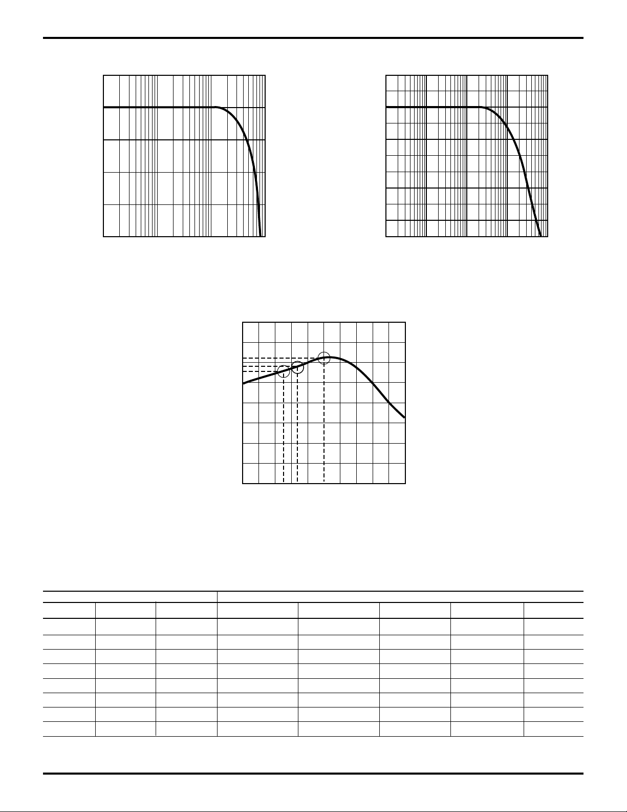
ML6429
1
0
–1
–2
AMPLITUDE (dB)
–3
–4
0 0.1 1 10
FREQUENCY (MHz)
Figure 1. Passband Flatness (Normalized)
All outputs. Passband is ripple-free.
90
70
20
0
–20
–40
AMPLITUDE (dB)
–60
–80
0.01 0.1 1 10010
FREQUENCY (MHz)
Figure 2. Passband/Stopband Rejection Ratios
(Normalized) All outputs.
50
DELAY (ns)
30
10
159
Figure 3. Group Delay, all Outputs
Low frequency group delay is 62ns. At 3.58MHz group
delay increases by only 4ns. At 4.43MHz group delay
increases by only 7ns. The maximum deviation from flat
group delay of 12ns occurs at 6MHz.
INPUTS OUTPUTS
A/B MUX SWAP CVF SWAP CVU CV
00 0CV
00 1CV
01 0CV
01 1CV
10 0CV
10 1CV
11 0CV
11 1CV
OUT
1/Y
INF
INF
INU
INU
INF
INF
INU
INU
FREQUENCY (MHz)
ACV
OUT
OUT
/Y1 CV
/Y1 CV
B/Y3 CV
B/Y3 CV
/Y1 CV
/Y1 CV
A/Y2 CV
A/Y2 CV
1137481026
2/Y
INU
INF
INU
INF
INU
INF
INU
INF
OUT
BR
OUT/YOUT
CG
OUT/YOUT
DB
OUT/COUT
B/Y3 RINB/Y5 GINB/Y7 BINB/C2
/Y1 RINB/Y5 GINB/Y7 BINB/C2
B/Y3 RINB/Y5 GINB/Y7 BINB/C2
/Y1 RINB/Y5 GINB/Y7 BINB/C2
A/Y2 RINA/Y4 GINA/Y6 BINA/C1
/Y1 RINA/Y4 GINA/Y6 BINA/C1
A/Y2 RINA/Y4 GINA/Y6 BINA/C1
/Y1 RINA/Y4 GINA/Y6 BINA/C1
Table 1. Selecting Composite, Luma, RGB, and Chroma Outputs
REV. 1.1 2/8/2001 7
Page 8

ML6429
TYPICAL APPLICATIONS
BASIC APPLICATIONS
The ML6429 provides channels for two banks of inputs for
RGB and composite video. The R and G channels can be
used as luma inputs while the B channel can be used as a
chroma input. Composite outputs and an H-sync output is
also provided. There are several configurations available
with the ML6429. Figure 4 includes a list of basic output
options for composite, S-video, TV modulator, and RGB
outputs. Note that each composite channel can drive a CV
load or a channel modulator simultaneously. The ML6429
standalone can be used as an EVC or SCART cable driver
with nine video sources (75Ω or low impedance buffer)
and seven video outputs. All inputs and outputs are AC
coupled. When driving seven loads, power dissipation
must be measured to ensure that the junction temperature
doesn't exceed 120ºC.
EVC CABLE DRIVING
The ML6429 can be configured to drive composite video,
S-video, and horizontal sync through an EVC connector
(Figure 5). Composite video and S-video inputs are filtered
through 4th-order Butterworth filters and driven through
internal 75Ω cable drivers. A buffered H-sync output is
also available.
SCART CABLE DRIVING
The ML6429 can be configured either as a SCART cable
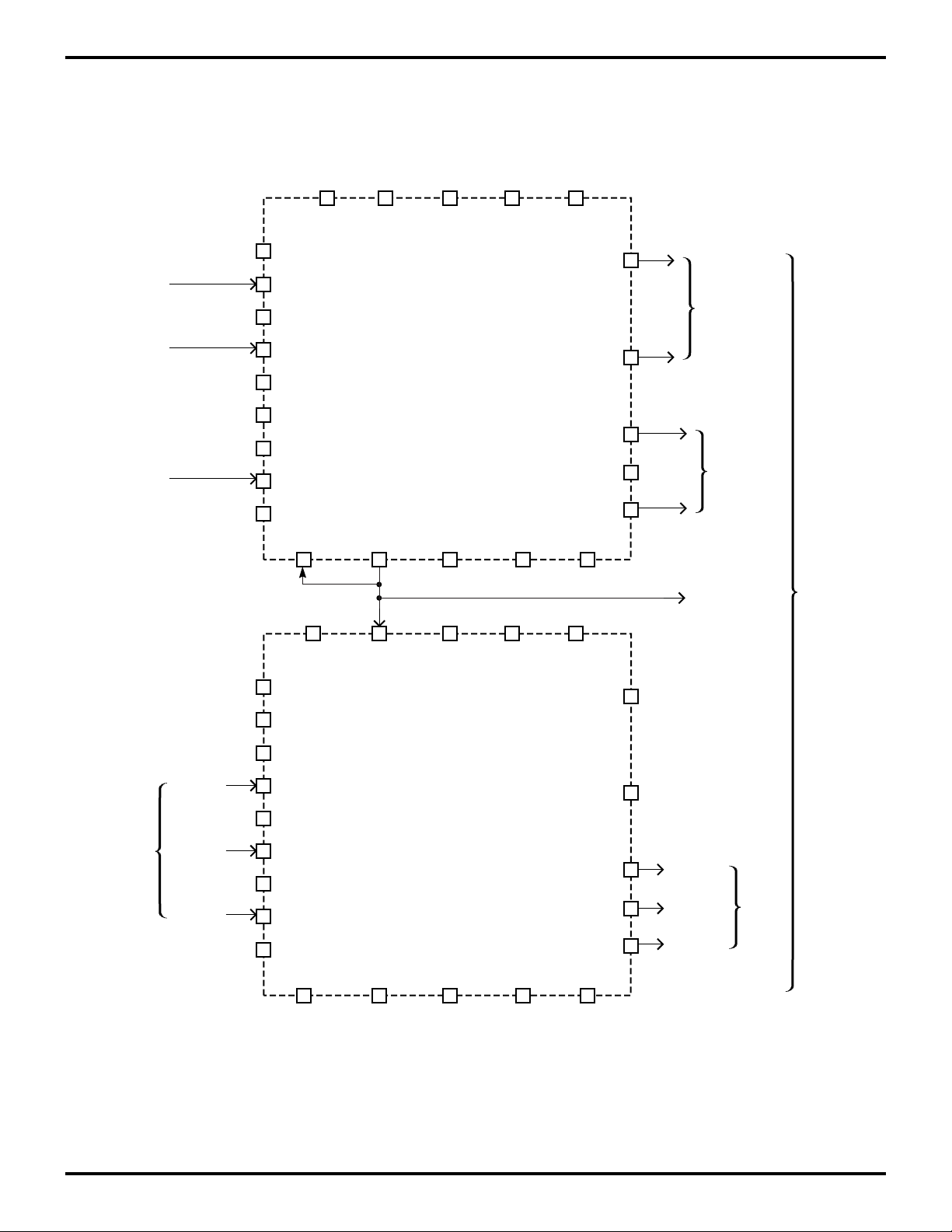
driver (Figure 4) or as a SCART cable driver and S-video
driver (Figure 6). A horizontal sync output is also available.
Note that the ML6429 can be used in a master-slave mode
where the sync-out from the master is used as the sync-in
of the slave; this allows the CV, S-video, and RGB channels
to operate under the same sync signals.
Note that in SCART applications, it is not always necessary
to AC couple the outputs. Systems using SCART
connectors for RGB and composite video can typically
handle between 0 and 2V DC offset (see DC Coupled
Applications section).
RGB APPLICATIONS
RGB video can be filtered and driven through the
ML6429. For sync suppressed RGB, the sync signal can be
derived from SYNCIN PIN.
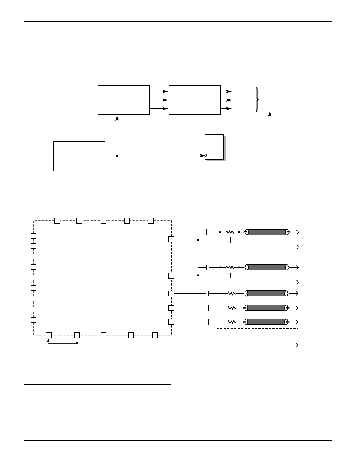
OSD (ON-SCREEN DISPLAY) APPLICATIONS
Unfiltered RGB video from an OSD processor needs to be
filtered and then synchronized to a fast blanking interval
or alpha-key signal for later video processing. With the
total filter delay being 80ns ±10ns, a D flip-flop or similar
delay element can be used to delay the fast blanking
interval or alpha-key signal, which synchronizes the RGB
and OSD signals (Figure 9).
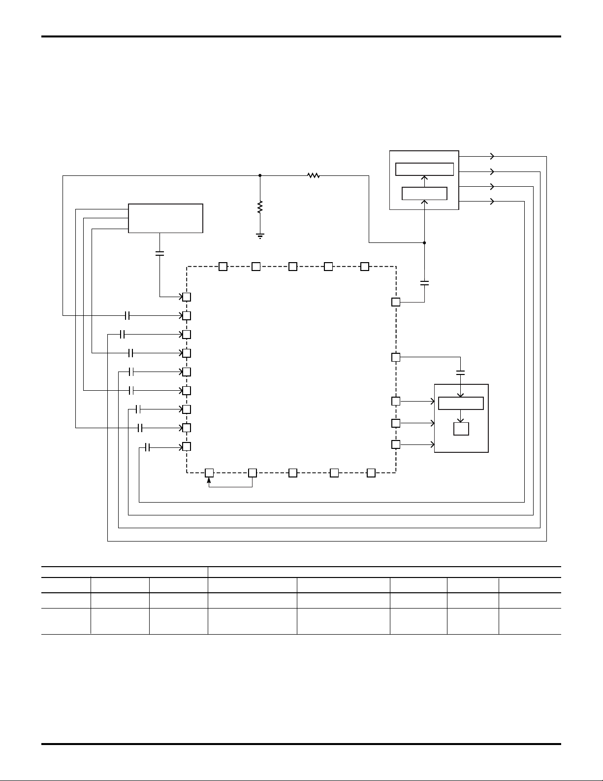
CHANNEL MULTIPLEXING
The ML6429 can be configured for multiple composite
channel multiplexing (Figure 8). Composite and RGB
sources such as VCRs, and digital MPEG 2 sources can be
selected using the ML6429 swap mux controls. A/B MUX,
SWAP CVU, and SWAP CVF signals can be used to select
and route from various input sources.
DC COUPLED APPLICATIONS
The 220µF capacitor coupled with the 150Ω termination
forms a highpass filter which blocks the DC while passing
the video frequencies and avoiding tilt. Lower values such
as 10µF would create a problem. By AC coupling, the
average DC level is zero. Thus, the output voltages of all
channels will be centered around zero.
Alternately, DC coupling the output of the ML6429 is
allowable. There are several tradeoffs: The average DC
level on the outputs will be 2V; Each output will dissipate
an additional 40mW nominally; The application will need
to accommodate a 1V DC offset sync tip; And it is
recommended to limit one 75Ω load per output. However,
if two loads are required to be driven at a time on the
composite output while DC coupling is used, then the
swap–mux and 5th line driver can be configured to enable
the filtered composite signal on both the 4th and 5th line
drivers. Thus, the composite load driving requirement is
divided into two line drivers versus one.
Required Setup: A composite or luma or green signal must
be present on CV
necessary sync signals to other channels (R,G,B,Y,C).
Otherwise, sync must be provided at the SYNCIN pin. For
RGB applications, the green channel with sync can be
used as an input to CV
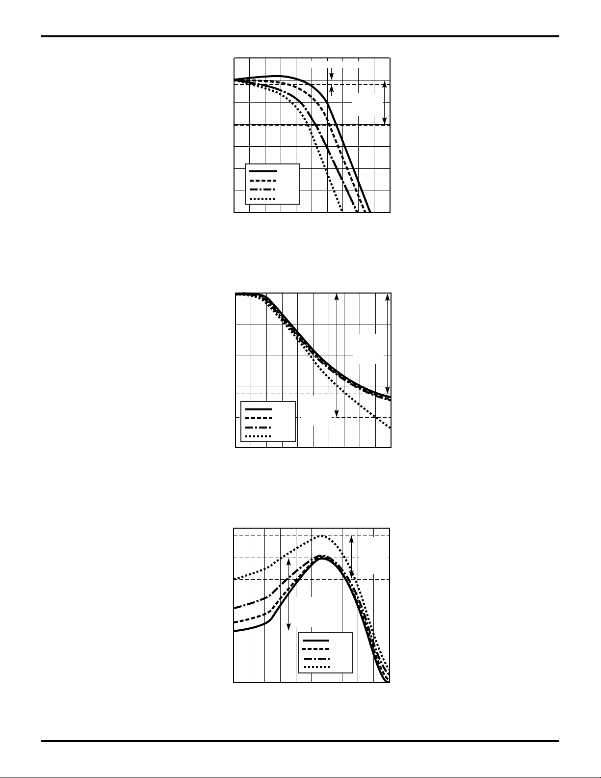
USING THE ML6429 FOR PAL APPLICATIONS
The ML6429 can be optimized for PAL video by adding
frequency peaking to the composite and S-video outputs.
Figure 10 illustrates the use of a additional external
capacitor (300pF), added in parallel to the output source
termination resistor. This raises the frequency response
from 1.0dB down at 4.8MHz (for no peaking cap) to 0.2dB
down at 4.8MHz (for 300 pF), which allows for accurate
reproduction of the upper sideband of the PAL subcarrier.
Figure 11 shows the frequency response of PAL video with
various values of peaking capacitors (0pF, 220pF, 270pF,
300pF) between 0 and 10MHz.
For NTSC applications without the peaking capacitor, the
rejection at 27MHz is 40dB (typical). For PAL applications
with the peaking capacitor, the rejection at 27MHz is
34dB (typical). (Figure 12). The differential group delay is
shown in Figure 13 with and without a peaking capacitor
(0pF, 220pF, 270pF, and 300pF) varies slightly with
capacitance; from 8ns to 13ns.
A/Y2 or CV
INU
INU
B/Y3 inputs to provide
INU
A/Y2 or CV
INU
B/Y3.
8 REV. 1.1 2/8/2001
Page 9
ML6429
19 5 17 22 6
GNDO V
CV
/Y1
INF
2
CV
A/Y2
INU
3
CV
B/Y3
INU
4
RINA/Y4
7
RINB/Y5
8
GINA/Y6
9
GINB/Y7
10
BINA/C1
11
BINB/C2
12
SYNCIN SYNCOUT SWAP CVU SWAP CVFA/B MUX
23 24 1 13 14
GND
CCO
ML6429
RGB V
CCO
INPUTS
Bank A: RGB, CV filtered path
Bank B: RGB, CV filtered path
Other: CV unfiltered path, Sync IN (slave mode)
CV V
CV
OUT
CV
OUT
R
OUT/YOUT
G
OUT/YOUT
B
CC
1/Y
OUT
2/Y
OUT
OUT/COUT
220µF
A
21
220µF
B
20
C
18
D
16
15
220µF
220µF
220µF
OPTIONAL FOR DC COUPLED APPLICATIONS
75Ω
75Ω
75Ω
75Ω
75Ω
VIDEO CABLES
CV/Y
MODULATOR
CV/Y
MODULATOR
R/Y
G/Y
B/C
H SYNC OUT
OUTPUTS
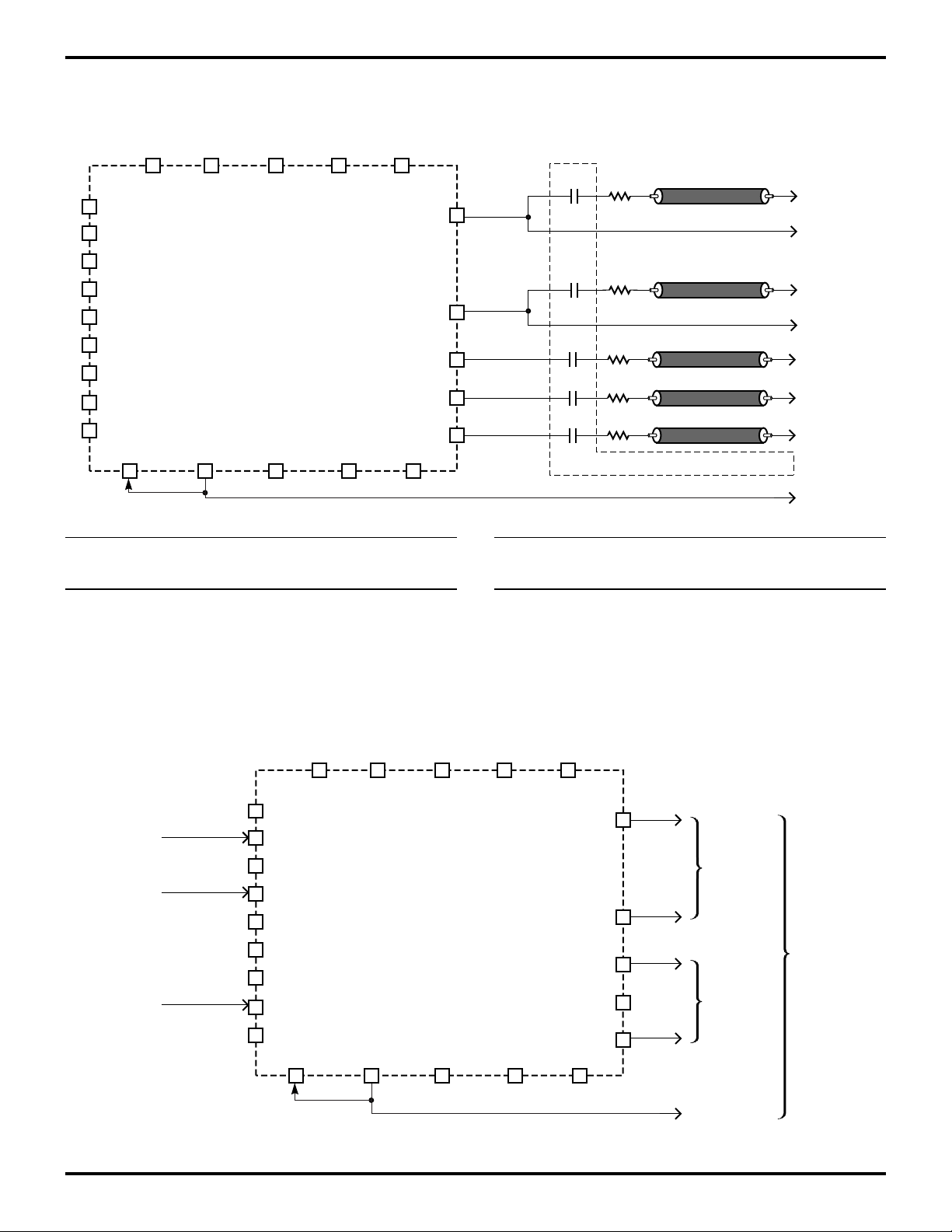
Option 1: 2 CV outputs + 2 TV modulator outputs, 1 RGB output
Option 2: 2 CV outputs + 1 TV modulator output, 1 S-video output
Other: Sync output (buffered stripped sync)
COMPOSITE
VIDEO IN
LUMA IN
CHROMA IN
Figure 4. Basic Application for NTSC
19 5 17 22 6
GNDO V
CV
/Y1
INF
2
CV
A/Y2
INU
3
CV
B/Y3
INU
4
RINA/Y4
7
RINB/Y5
8
GINA/Y6
9
GINB/Y7
10
BINA/C1
11
BINB/C2
12
SYNCIN SYNCOUT SWAP CVU SWAP CVFA/B MUX
23 24 1 13 14
GND
CCO
ML6429
RGB V
CCO
CV V
CV
OUT
CV
OUT
R
OUT/YOUT
G
OUT/YOUT
B
CC
1/Y
OUT
2/Y
OUT
OUT/COUT
A
B
C
D
21
20
18
16
CHROMA
15
LUMA
OUT
OUT
COMPOSITE
VIDEO OUT
TO EVC
CONNECTOR
S-VIDEO
OUT
H SYNC OUT
Figure 5. EVC (Enhanced Video Connector) Application: S-Video, Composite, plus H-Sync out
REV. 1.1 2/8/2001 9
Page 10
ML6429
COMPOSITE
VIDEO IN
LUMA IN
CHROMA IN
CV
2
CV
3
CV
4
RINA/Y4
7
RINB/Y5
8
GINA/Y6
9
GINB/Y7
10
BINA/C1
11
BINB/C2
12
19 5 17 22 6
GNDO V
/Y1
INF
A/Y2
INU
B/Y3
INU
GND
CCO
ML6429
RGB V
CCO
CV V
CV
OUT
CV
OUT
R
OUT/YOUT
G
OUT/YOUT
B
CC
1/Y
OUT
2/Y
OUT
OUT/COUT
A
B
C
D
21
20
18
16
15
LUMA
OUT
CHROMA
OUT
COMPOSITE
VIDEO OUT
S-VIDEO
OUT
R INPUT
G INPUTRGB INPUT
B INPUT
SYNCIN SYNCOUT SWAP CVU SWAP CVFA/B MUX
23 24 1 13 14
24 23 17 22 6
SYNC OUT V
CV
/Y1
INF
2
CV
A/Y2
INU
3
CV
B/Y3
INU
4
RINA/Y4
7
RINB/Y5
8
GINA/Y6
9
GINB/Y7
10
BINA/C1
11
BINB/C2
12
GNDO GND SWAP CVU SWAP CVFA/B MUX
19 5 1 13 14
SYNC IN
ML6429SLAVE
CCO
RGB V
CCO
CV V
CV
OUT
CV
OUT
R
OUT/YOUT
G
OUT/YOUT
B
CC
1/Y
OUT
2/Y
OUT
OUT/COUT
H SYNC OUT
A
21
B
20
C
D
R OUTPUT
18
RGB
G OUTPUT
16
B OUTPUT
15
VIDEO
OUT
TO SCART
CONNECTOR
Figure 6. SCART (Peritel) + S-Video Application: S-Video, RGB, Composite, plus H-Sync out
10 REV. 1.1 2/8/2001
Page 11
ML6429
B
DIGITAL PLAYER
G
OR MPEG-2 DECODER
R
COMPOSITE VIDEO IN
Y
U
V
0.1µF
0.1µF
0.1µF
0.1µF
0.1µF
0.1µF
0.1µF
0.1µF
0.1µF
CV
CV
CV
G
R
B
1
2
3
GNDO V
CV
/Y1
INF
2
CV
A/Y2
INU
3
CV
B/Y3
INU
4
RINA/Y4
7
RINB/Y5
8
GINA/Y6
9
GINB/Y7
10
BINA/C1
11
BINB/C2
12
1kΩ
1kΩ
19 5 17 22 6
GND
CCO
ML6429
RGB V
CCO
CV V
CV
OUT
CV
OUT
R
OUT/YOUT
G
OUT/YOUT
B
OUT/COUT
CC
1/Y
2/Y
OUT
OUT
A
21
B
20
C
18
D
16
15
VCR
VIDEO RECORDER
MODULATOR
220µF
CV
OUT1
COMPOSITE VIDEO OUT, CV
R
G
B
OUT
OUT
OUT
MODULATOR
TV
TV
CV
R
G
B
OUT2
220µF
SYNCIN SYNCOUT SWAP CVU SWAP CVFA/B MUX
23 24 1 13 14
INPUTS OUTPUTS
A/B MUX SWAP CVU SWAP CVF CV
1CV
OUT
OUT
2R
OUT
G
OUT
0 0 0 Digital Player VCR VCR VCR VCR
1 0 1 Digital Player Digital Player Digital Digital Digital
Player Player Player
Figure 7. Multi-Source CV and RGB Channels
B
OUT
REV. 1.1 2/8/2001 11
Page 12
ML6429
OSD
(ON-SCREEN DISPLAY)
PROCESSOR
ML6431
GENLOCK/CLOCK
GENERATOR
13.5MHz/
27MHz
Figure 8. Synchronizing the Filter Delay with Fast Blanking or Alpha-Key Signals in OSD Applications
19 5 17 22 6
GNDO V
CV
/Y1
INF
2
CV
A/Y2
INU
3
CV
B/Y3
INF
4
RINA/Y4
7
RINB/Y5
8
GINA/Y6
9
GINB/Y7
10
BINA/C1
11
BINB/C2
12
SYNCIN SYNCOUT SWAP CVF SWAP CVUA/B MUX
23 24 1 13 14
GND
CCO
ML6429
RGB V
CCO
UNFILTERED
R
G
B
FAST BLANKING INTERVAL
OR ALPHA-KEY SIGNAL
CV V
CV
OUT
CV
OUT
R
OUT/YOUT
G
OUT/YOUT
B
OUT/COUT
CC
1/Y
2/Y
OUT
OUT
A
21
B
20
C
18
D
16
15
80ns±10ns DELAY FILTERED
R
75Ω
75Ω
75Ω
75Ω
75Ω
OUTPUT
G
OUTPUT
B
OUTPUT
330pF
330pF
ML6429
SCART/QUAD VIDEO
FILTER AND DRIVER
DQ
Standard
74XX
D'FF
DELAY AT 13.5MHz IS APPROXIMATELY 74ns
220µF
220µF
220µF
220µF
220µF
NOT REQUIRED FOR DC COUPLED APPLICATIONS
TO MUX OR
OTHER
PROCESSING
FAST BLANKING
INTERVAL
OR ALPHA-KEY
SIGNAL
VIDEO CABLES
CV/Y
MODULATOR
CV/Y
MODULATOR
R/Y
G/Y
B/C
H SYNC OUT
INPUTS
Bank A: RGB, CV filtered path
Bank B: RGB, CV filtered path
Other: CV unfiltered path, Sync IN (slave mode)
OUTPUTS
Option 1: 2 CV outputs + 2 TV modulator outputs, 1 RGB output
Option 2: 2 CV outputs + 1 TV modulator output, 1 S-video output
Other: Sync output (buffered stripped sync)
Figure 9. Basic Application for PAL
12 REV. 1.1 2/8/2001
Page 13
–0.5
0
0
15793
268104
ML6429
0.2dB WITH PEAKING
0.5
1dB
WITHOUT
PEAKING
1
1.5
AMPLITUDE (dB)
2.5
2
3
0
15793
300pF
270pF
220pF
0pF
268104
FREQUENCY (MHz)
Figure 10. NTSC/PAL Video Frequency Response With and Without Peaking Capacitor
0
–10
NTSC/PAL
–34dB
–20
WITH
PEAKING
–30
AMPLITUDE (dB)
–40
–50
0121830246
31521279
300pF
270pF
220pF
0pF
NTSC/PAL
–40dB
WITHOUT
PEAKING
FREQUENCY (MHz)
Figure 11. Stopband Rejection at 27MHz With and Without Peaking Capacitor
10
8ns
GROUP
DELAY
WITHOUT
PEAKING
0
13ns GROUP
DELAY
DELAY (ns)
–10
–20
0461082
15793
WITH 330pF
PEAKING
300pF
270pF
220pF
0pF
FREQUENCY (MHz)
Figure 12. Group Delay at 5.5MHz (PAL) With and Without Peaking Capacitor
REV. 1.1 2/8/2001 13
Page 14
ML6429
CVIN1
CVIN2
YIN1
YIN2
CIN
R7
1kΩ
JP2
123
HSYNCIN
123
CIN2
JP5
32 1
LEGEND
JPx
PERMANENT
SHORT
R24 75Ω
R23 75Ω
R22 75Ω
R21 75Ω
R20 75Ω
R17 75Ω CV
R16 75Ω
R15 75Ω
R14 75Ω
CV
CV
CV
Y
C
5V
JP3
12 3
JP4
123
B
G
R
Y
Y
OUT
OUT
OUT
OUT
OUT
OUT
OUT
OUT
Y+
OUT
OUT
OUT
1
2
1
2
1
2
1
+
P2—EVC
13
14
15
5
4
5
9
13
17
21
19
16
7
11
15
P1—SCART
21
20
18
16
15
21
20
18
16
15
MOVABLE
JUMPER
C2 220µF
C3 220µF
C4 220µF
C5 220µF
C6 220µF
C7 220µF
C8 220µF
C9 220µF
123
220µF
C33 330pF
C34 330pF
SW1-A
SW1-B
5V
1
GND
R1 75Ω
R2 75Ω
R3 75Ω
R4 75Ω
R5 75Ω
R6 1kΩ
JP1
123
GND
C14 0.1µF
C15 0.1µF
C16 0.1µF
C17 0.1µF
C18 0.1µF
C19 0.1µF
0.1µF
C20
C12 1µF
C13 0.1µF
2
3
4
7
8
9
10
11
12
SW1-C
FB1
V
CCA
6 1722 195
MUX
MUX
MUX
MUX
1 14132423
1 14132423
V
CCO
FOURTH
ORDER
FILTER
FOURTH
ORDER
FILTER
FOURTH
ORDER
FILTER
FOURTH
ORDER
FILTER
FB2
C10 1µF
C11 0.1µF
U2
X2
MUX
X2
X2
X2
X2
U2
C21 0.1µF
R8 1kΩ
JP6
R9 1kΩ
B
IN
R10 1kΩ
G
IN
R11 75Ω
R
IN
R12 75Ω
R13 75Ω
C22 0.1µF
C23 0.1µF
C24 0.1µF
C25 0.1µF
C26 0.1µF
C27 0.1µF
C28
2
3
4
7
8
9
10
11
12
0.1µF
MUX
MUX
MUX
MUX
C29 1µF
C30 0.1µF
V
CCA
FOURTH
ORDER
FILTER
FOURTH
ORDER
FILTER
FOURTH
ORDER
FILTER
FOURTH
ORDER
FILTER
X2
X2
X2
C31 0.1µF
C32 0.1µF
V
CCO
X2
MUX
X2
56192217
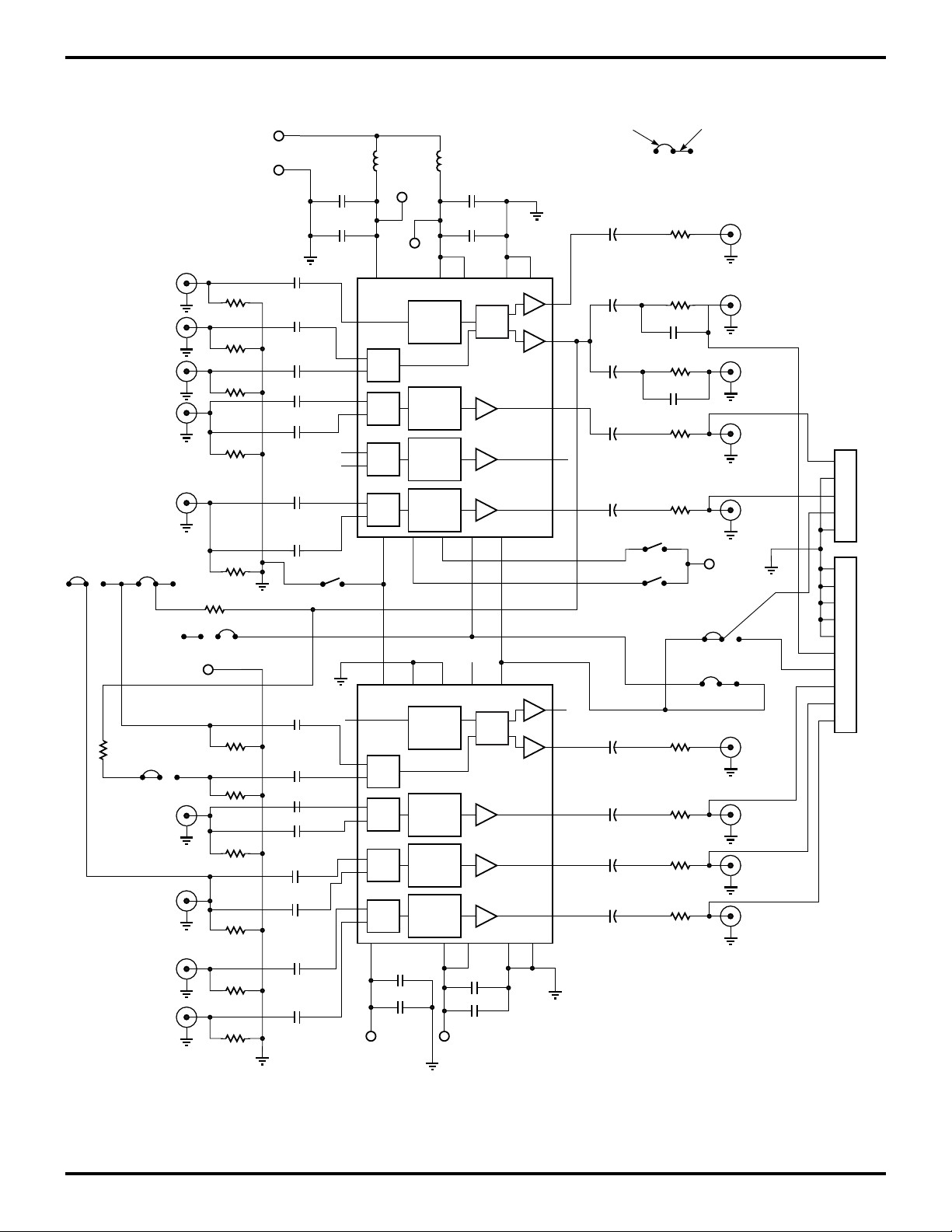
Figure 13. Schematic
14 REV. 1.1 2/8/2001
Page 15
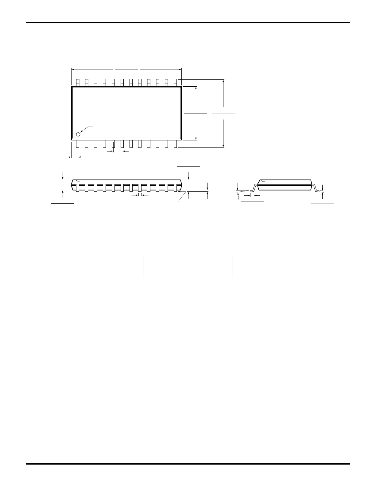
PHYSICAL DIMENSIONS inches (millimeters)
Package: S24
24-Pin SOIC
0.600 - 0.614
24
(15.24 - 15.60)
ML6429
PIN 1 ID
0.024 - 0.034
(0.61 - 0.86)
(4 PLACES)
0.090 - 0.094
(2.28 - 2.39)
1
0.050 BSC
(1.27 BSC)
0.012 - 0.020
(0.30 - 0.51)
ORDERING INFORMATION
PART NUMBER TEMPERATURE RANGE PACKAGE
ML6429CS-1 0°C to 70°C 24 Pin SOIC (S24)
0.291 - 0.301
(7.39 - 7.65)
0.095 - 0.107
(2.41 - 2.72)
SEATING PLANE
0.398 - 0.412
(10.11 - 10.47)
0.005 - 0.013
(0.13 - 0.33)
0º - 8º
0.022 - 0.042
(0.56 - 1.07)
0.009 - 0.013
(0.22 - 0.33)
DISCLAIMER
FAIRCHILD SEMICONDUCTOR RESERVES THE RIGHT TO MAKE CHANGES WITHOUT FURTHER NOTICE TO
ANY PRODUCTS HEREIN TO IMPROVE RELIABILITY, FUNCTION OR DESIGN. FAIRCHILD DOES NOT ASSUME
ANY LIABILITY ARISING OUT OF THE APPLICATION OR USE OF ANY PRODUCT OR CIRCUIT DESCRIBED HEREIN;
NEITHER DOES IT CONVEY ANY LICENSE UNDER ITS PATENT RIGHTS, NOR THE RIGHTS OF OTHERS.
LIFE SUPPORT POLICY
FAIRCHILD’S PRODUCTS ARE NOT AUTHORIZED FOR USE AS CRITICAL COMPONENTS IN LIFE SUPPORT DEVICES
OR SYSTEMS WITHOUT THE EXPRESS WRITTEN APPROVAL OF THE PRESIDENT OF FAIRCHILD SEMICONDUCTOR
CORPORATION. As used herein:
1. Life support devices or systems are devices or systems
which, (a) are intended for surgical implant into the body,
or (b) support or sustain life, and (c) whose failure to
perform when properly used in accordance with
2. A critical component in any component of a life support
device or system whose failure to perform can be
reasonably expected to cause the failure of the life support
device or system, or to affect its safety or effectiveness.
instructions for use provided in the labeling, can be
reasonably expected to result in a significant injury of the
user.
www.fairchildsemi.com © 2000 Fairchild Semiconductor Corporation
REV. 1.1 2/8/2001 15
 Loading...